B
SERVICE MANUAL
MODEL
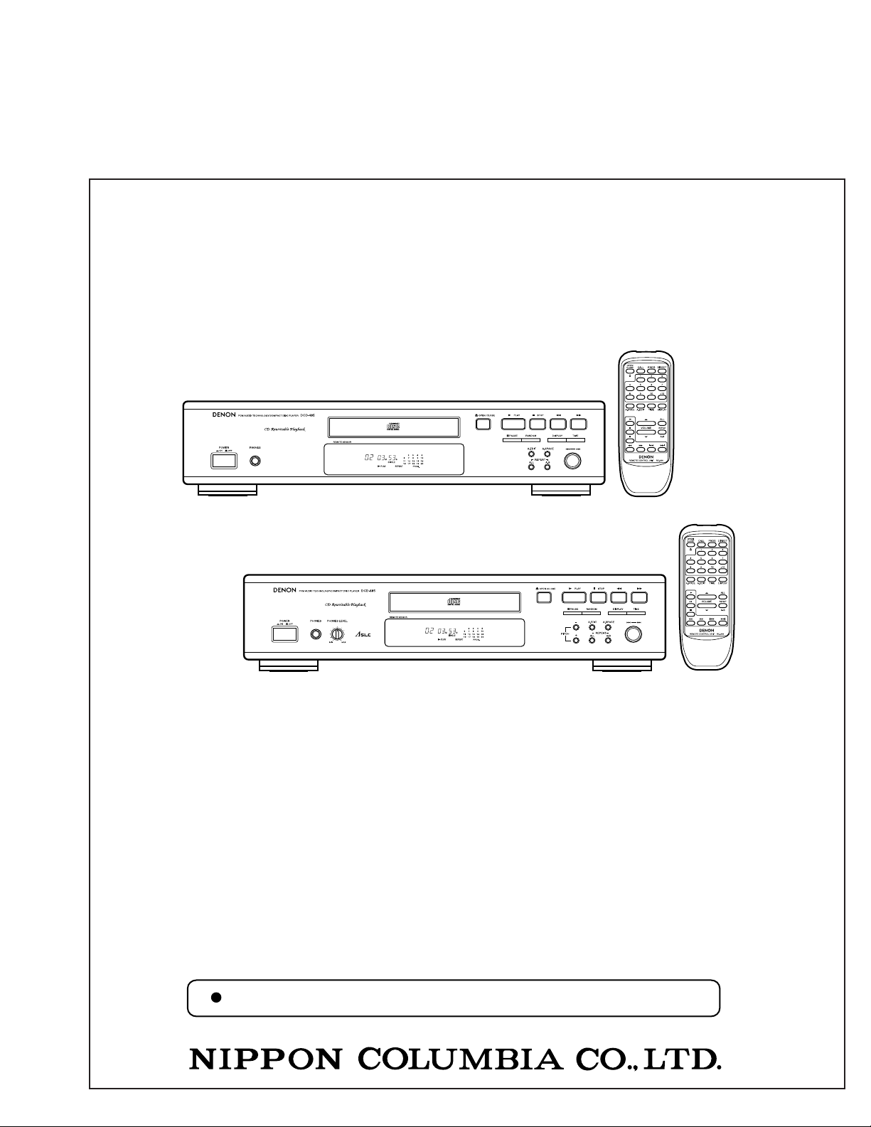
DCD-485/685
STEREO CD PLAYER
DCD-485
Hi-Fi Component
DCD-685
Some illustration using in this service manual is slightly from the actual set.
2
SAFETY PRECAUTIONS
SAFETY PRECAUTIONS
The following check should be performed for the continued prtection of the customer and service
technician.
LEAKAGE CURRENT CHECK
Before reterning the unit to the customer,make sure you make either (1) a
leakage current check or (2) a line to chassis resistance check. If the leakage current exceeds 0.5
miliamps, or if hte resistance from chassis to either side of the power cord is less than 460 kohms,
the unit is detective.
SPECIFICATIONS
SPECIFICATIONS
DCD-485
AUDIO
Number of Channels:
Freqency Responese:
Dynamic Range:
Signal to Noise ratio:
Harmonic distortion:
Separation:
Wow and Flutter:
Output Voltage:
DISCS
GENERAL CHARACTERISTICS
Power consumption: 11 W
Dimensions:
Mass: 3.4 kg
FUNCTIONS AND DISPLAY
Functions:
Others:
REMOTE CONTROL UNIT
Remote Control System:
Mass: 85 g including batteries
2 channels
2 to 20 kHz
98 dB
105 dB
0.003 % (1 kHz)
102 dB (1 kHz)
Below measurable limit:
( 0.001
0.2 to 2.0 V
Compact Disc format
AC 230 V, 50 Hz Power Supply:
434 (W) x 100 (H) x 285 (D) mm
Automatic searchi, programmed playback, repeat playback, manual search, auto space,
time mode, auto edit, dimmer, random playback, pitch control (DCD-685 only)
Track number, time, music calendar and engaged modesDisplay:
Headphones jack
RC-266
Infrared pulse system
3V DC; two R6P (standard size AA) dry cell batteriesPower Supply:
54.5 (W) x 140 (H) x 24.8 (D) mmExternal Dimensions:
% W. peak)
DCD-685
100 dB
110 dB
103 dB (1 kHz)
12 W
3.6 kg
✽ Specifications and design are subject to change without notice for purpose of improvement.
3
DISASSENBLY
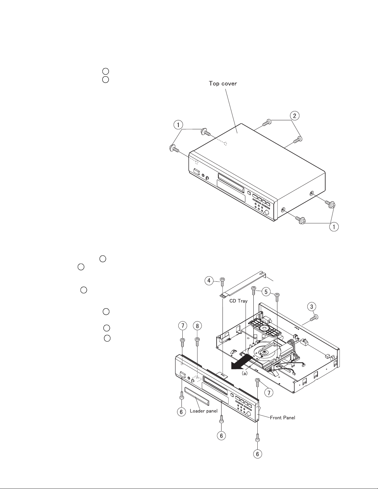
Follow the procedure below in reverse order when reassembling
(Follow the procedure below in reverse order when reassembling)
1. Top Cover
1. Remove 4 screws
2. Remove 2 screws
3. Detach the Top Cover as shown in the fig.
on both sides.
1
on the Rear Panel.
2
2. Front Panel
1. Remove 1 screw 3 on the Rear Panel and
1 screw
(only DCD-485)
2. Take off the Mecha Cover after removing
2 screws
Open the Tray by turning the Gear (a) clockwise,
then detach the Loader Panel.
3. Remove 3 screws
Front Panel.
4. Remove 2 screws
Panel and 1 screw
fixing Support Bracket (b).
4
.
5
on the bottom edge of the
6
, at L/R ends of the Front
7
fixing Phone P.W.B.
8
Support Bracket

3. CD Mecha. Unit
1. Remove 4 screws
2. Unplug Connectors (b), (c) and FFC from each
socket.
3. Release the FFC from the Clamper.
fixing the CD Mecha.
9
4. Main P.W.B.
1. Remove 5 screws 10, 5 screws
Panel and detach it.
2. Remove 3 screws
3. Unfasten 1 P.W.B. Holder to detach the Main
P.W.B.
4. Remove 1 screw
Power P.W.B.
5. Unfasten 1 P.W.B. Holder to detach the Power
P.W.B.
fixing the Main P.W.B.
12
and 2 screw fixing the
on the Rear
11
4
5
CD TEST MODE
z
Setting of the test mode
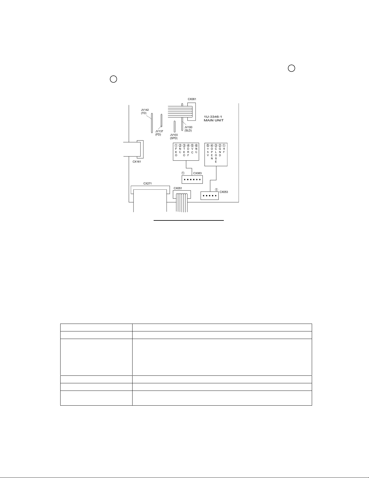
How to start the test mode: Turn on the power in the condition that CLOSE (Pin No. 3 )
and OPEN (Pin No. 4 ) of CX053 are being shorted. ( “01” is indicated on the DISPLAY)
To exit from the test mode, turn off the power.
(Refer to Fig. 1 “Test Point Layout”)
Fig. 1 “Test Point” Layout
* Laser light of the pickup is always emitted regardless of DISC loading in the test mode.
You may lose your eyesight if you look into the laser directly.
So be careful enough when operating in the test mode.
z
Used DISC: A-BEX TCD784
z
Explanation of each button
* Use only the buttons described below for operations while in the test mode,
and don’t push any other buttons.
Names of buttons Operation
OPEN / CLOSE * Loads or unloads DISC
PLAY * Emits laser light
* Repeats search operation (No DISC condition: While it’s
pressed)
* Actuates focus servo (In case of DISC loaded)
* Actuates tracking servo
STOP * Stops operation
PAUSE * Performs auto adjustment
MANUAL SEARCH
* Moves pickup
FORWARD / REVERSE
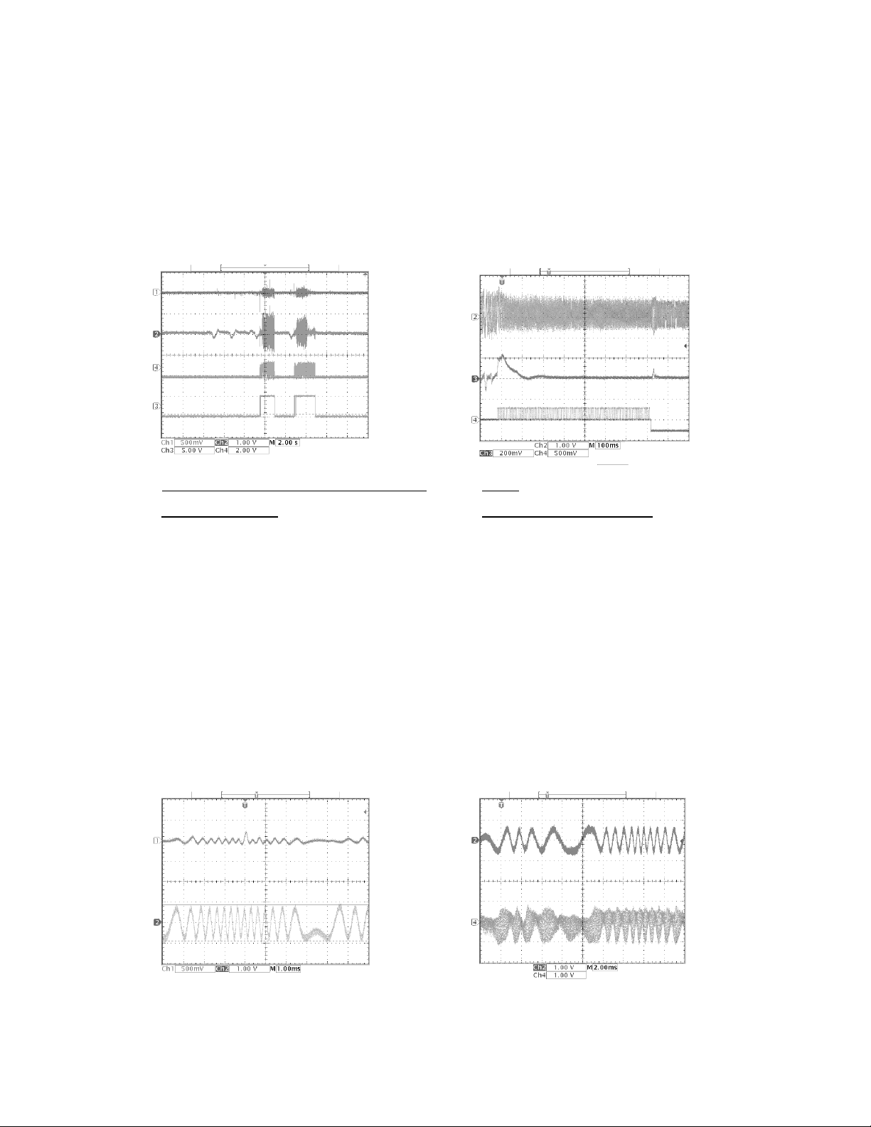
z
How to check the test mode
( 1 ) DISC discrimination, adjustment
* Insert DISC, and press the PAUSE button.
* “06 Adj” is displayed, and discrimination of DISC size 8 cm/12 cm, discrimination of
DISC reflectance (CD, CD-R/CD-RW), adjustment of focus, tracking offset,
and EF balance will be performed. (Adjusted values are not displayed:
FEO
TEO
HF
DRF
Fig. 2 DISC discrimination, adjustment Fig. 3
TEO
TB
SLD
Refer to Fig. 2, 3)
(Case of CD-RW) Adjustment of EF balance
* After completing the discrimination and adjustment, it becomes stop condition.
* Once discrimination of DISC has been carried out in the “06 Adj” mode, discrimination of
size and reflectance is no longer made, and only adjustment will be performed.
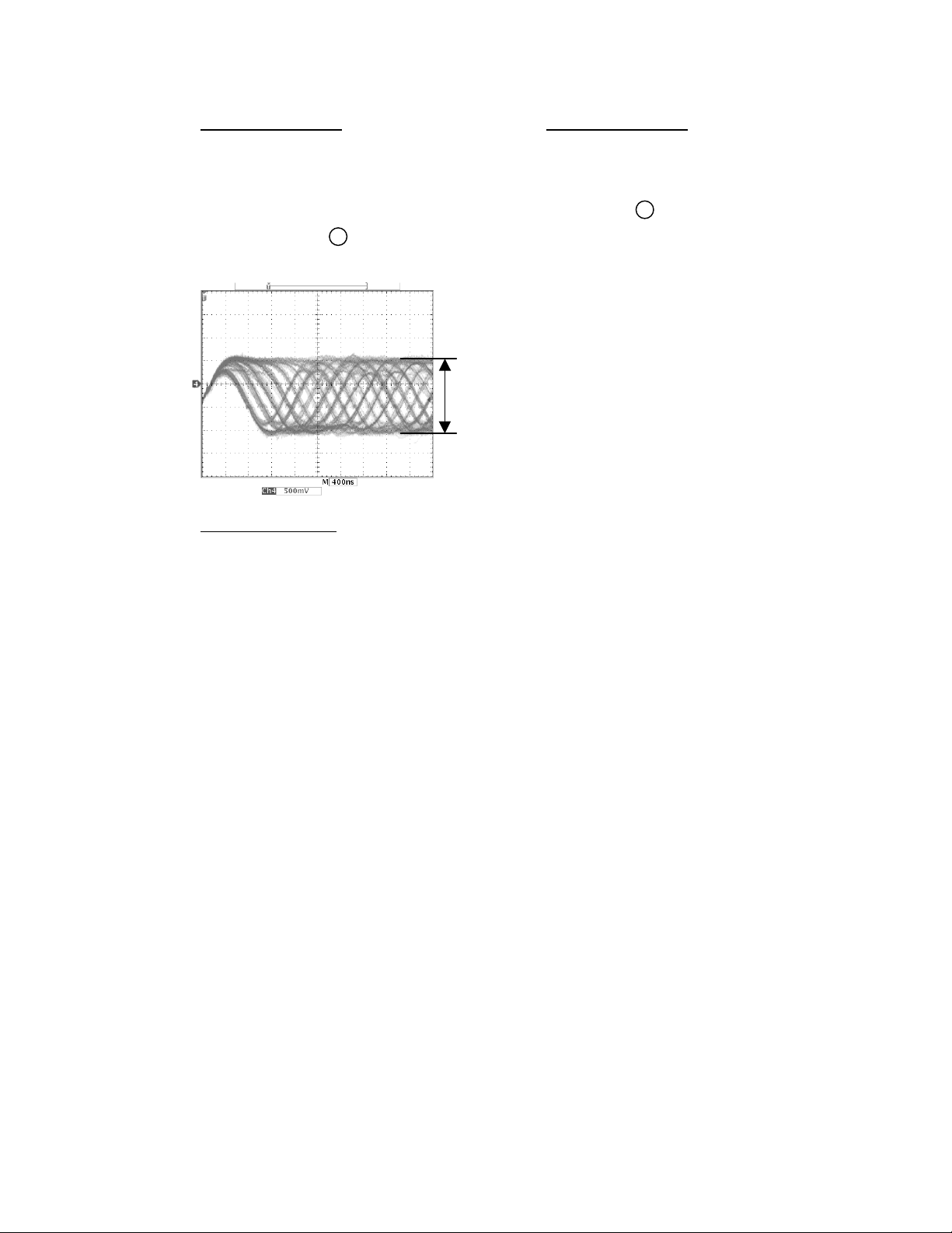
( 2 ) Checking of servo state
* Press the PLAY button after performing above (1) “DISC discrimination, adjustment”.
* “02 L on” is displayed, and the laser will start to light. (The pickup may vibrate with a rattling
noise if DISC has been loaded, but this is not abnormal.)
* Press the PLAY button again.
* “03 F on”is displayed. DISC starts turning,and focus servo will be actuated.
FEO
TEO
TEO
HF
(Refer to Fig. 4, 5)
6
¥¥¥
Fig. 4 In “03 F on”
¥¥¥ ¥¥¥¥¥¥¥¥¥
Fig.
5 In “03 F on”
* Press the PLAY button again.
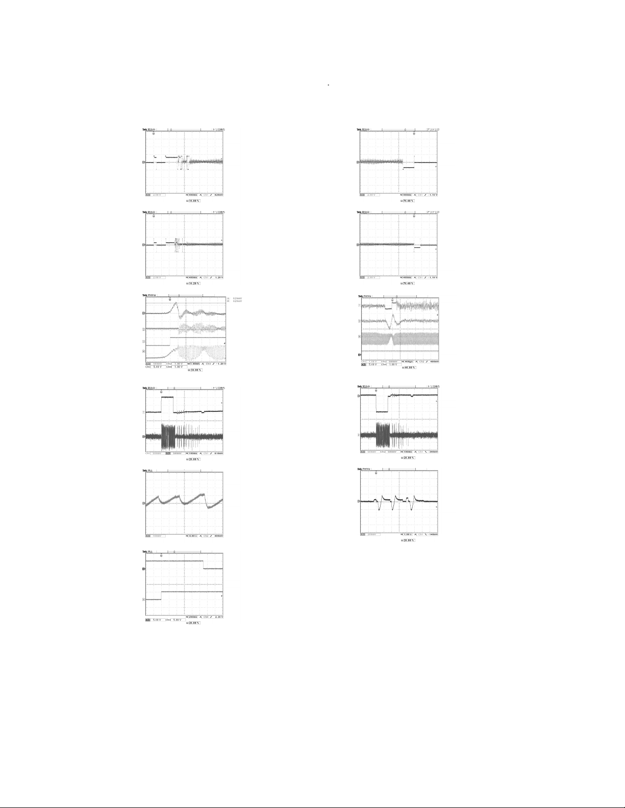
* “04 t on” is displayed. Tracking, CLV, and slide servo will be actuated.
* Monitor HF signal using the test terminals, HF of CX053 (Pin No. 1 ) and
VC of CX063 (Pin No. 5 : 2.5V ref. signal). Check that the signal’s amplitude
is 1.5Vâ0.3Vp-p. (Refer to Fig. 6)
HF
¥¥¥
A ( A = 1.5 ± 0.3 V
Fig. 6 In “04 t on”
P-P
)
7
8
p
Wave-forms of each point
SPD
SPD
FEO
TEO
DRF
HF
SLD
TEO
When 12 cm DISC
start
When 8 cm DISC
start
When focus servo
on
Track search
(when forward)
SPD
SPD
TD
TEO
HF
DRF
SLD
TEO
When 12 cm DISC
stop
When 8 cm DISC
stop
During PAUSE
Track search
(when reverse)
SLD
OPEN
CLOSE
During PLAY
When the tray
OPEN
FD
Focus search
(no DISC)
9
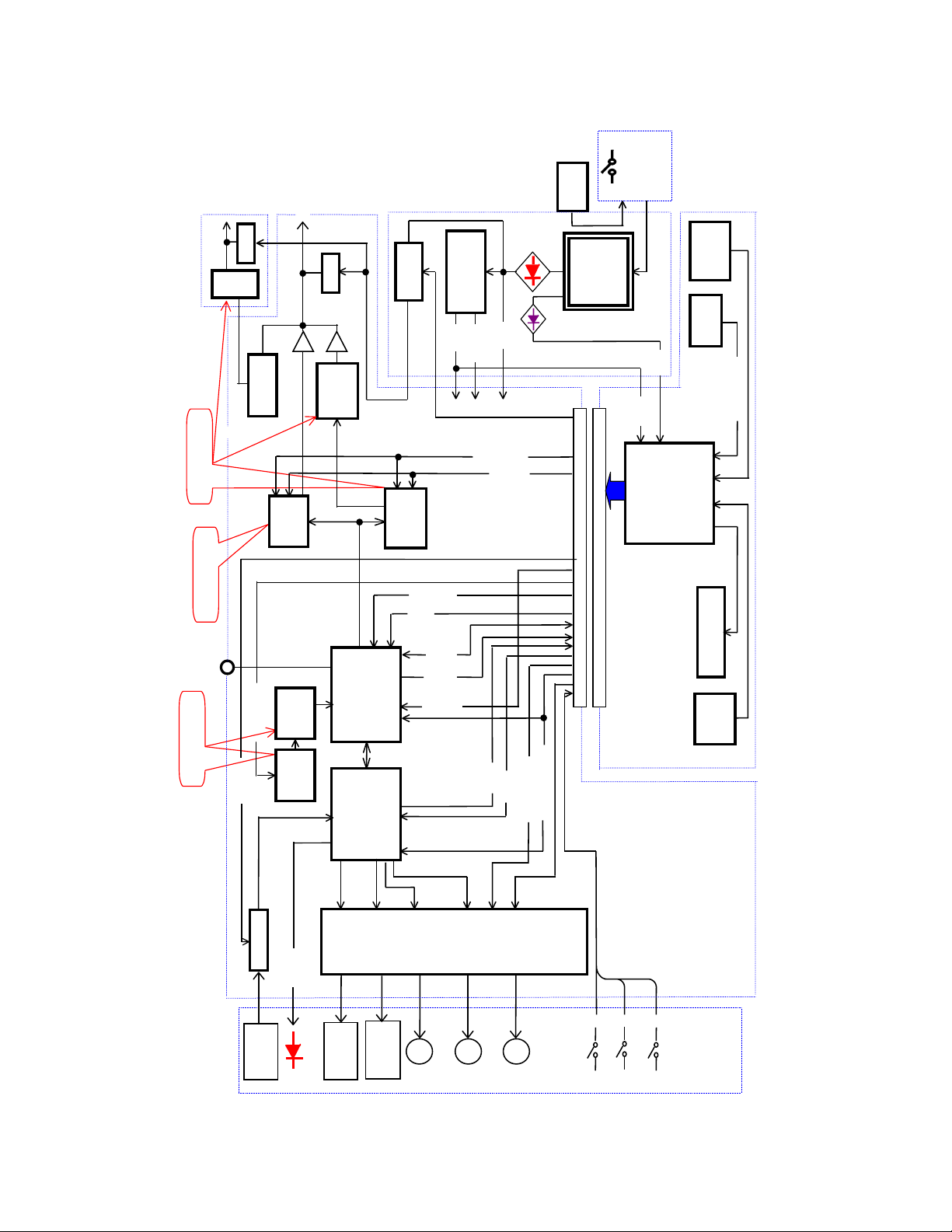
BLOCK DIAGRAM
MUTE
H/P UNIT
1U-3346-4
V
1U-3346-5
AC
INLET
POWER CONT.
±5V
IC501
M5290P
RESET
±8V
CONTROL
XRST2
MUTE
IC315
H/P AMP
DAC
PCM1702
IC602/603
MUTE
CONTROL
POWER SW
S616
ROTALY
PT501
TRANS.
POWER
POWER
1U-3346-2
-HB
DD
+V
ENCODER
UNIT
KEY
MATRIX
A/D INPUT
DCD-685 only
IC105
DF&DAC
PCM1735
DCD-485 only
OPT.OUT
DSP
VCO
IC108
TC9246F
CONTROL
DCD-685 only
PLL
IC107
CD/RW
BU2616F
LC78625E
ASP
LA9241M
D.FILTER
SM5841BS
IC102
IC101
2
IC703
MD
D.MUTE
CODE
SUB
FSEQ
XRST1
DRF
CX271
CY271
1U-3346-3
SL
DRV.MUTE
COTROL BUS
µ-COM
µPD78044F
DISPLAY
1U-3346-1
MAIN UNIT
IC201
VFD
REMOTE
FL601
IC702
SENSOR
RW SW
UP
PICK
LD ON
L.DIODE
FOCUS
FOCUS
COIL Drv.
COIL
SLIDE
COIL Drv.
TRACKING
M
COIL
TRACKIN
Mtr Drv.
Mtr. Drv.
SPINDLE
LOADING
M
SLIDE
M
SPINDLE
IC104
LA6995
Mtr. Drv.
LOADING
OPEN-SW
INMOST-SW
CD MECHA
CLOSE-SW
KSL-2130CCM
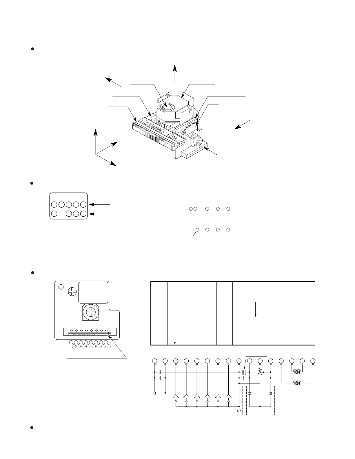
10
NOTE FOR HANDLING OF LASER PICK-UP
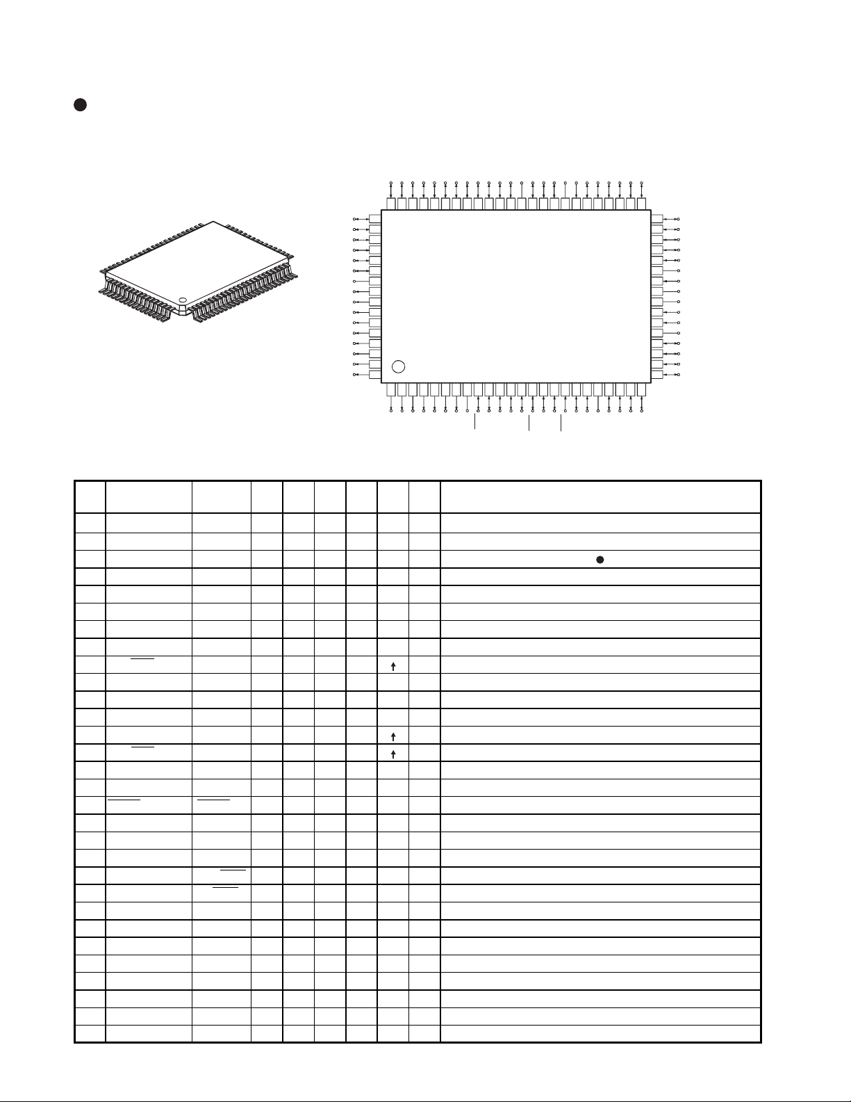
Description of the Components
+Z-axis direction
Label
+X-axis direction
KSS-213C
Z-axis
OP Slide base
Slide rack
Y-axis
(Tangental direction)
X-axis
(Radial direction)
Lot No.
lop
Object Lens
Actuator cover
PAL-2 Flexible board
Label
+Y-axis direction
Flexible flat cable connector
year
(last figure)
day month quality control No.
Lot No.
Oct. Nov. and Dec. are ex pressed by alphabetical letters
of X, Y and Z.
lop No.
10 1 10
LD drive currentquality control
The expressed unit is by mA, with omission of the
decimal point as for example, 56.5mA will be expressed as 565, but the head of English letter means
the control in the manufacturning plant.
-1
Pin Connector
KSS-213C
Pin No. Description
1 PD IC Vc IN
2 Vcc IN
3 E OUT
4 D OUT
5 A OUT
6 B OUT
7 C OUT
1 3 5 7 9 11 13 15
2 4 6 8 10 12 14 16
8 F OUT
Flexible flat cable connector
+2.5V +5V
CAUTION: The soldered connecting portion must be bridged when removing CX161.
IN/OUT
Pin No. Description
10 LD LD IN
11 VR IN
12 PD OUT
13 FCS (+) IN
14 TRK (+) IN
15 TRK (−)IN
16 FCS (−)IN
987654321
LD
IN/OUT
9 GND IN
PDIC
SHORT LAND
10
11
LDPDIC
13
12
14
15
TRACKING
FOCUSING
16

Caution for Handling the Laser Pick-up
The laser pick-up KSS-213C is assembled and precisely
adjusted using a sophisticated manufacturing process in our
plant. Do not disassemble or attempt to readjust it. Please
observe the following instructions carefully in handling the
pick-up.
1. Handle with Care
(1) Storage
Do not store the pick-up in dusty, high-temperatured or
high-humidity environments.
(2) Please take care for preventing from shock by falling
down or careless handling.
2. Laser Diode (LD)
(1) Protect your eyes
The laser beam may damage the human eye, since the
intensity of the focused spot may reach 7×10
2
W/cm
even if the intensity at the objective lens is 400µW
maximum. As the light beam spreads after focused
through the objective lens, it does not effect you in the
place as far as more than 30 cms. However, do not look
at the laser light beam either through the objective lens
directly nor another lens or a mirror.
(2) Poison of As
Since the LD chip contains As (Arsenic), as GaAs +
GaAlAs, as known as the poison, although the poison is
relatively weak, in comparing with others, e.g. As
etc., and the amount is small, avoid putting the
AsCl
3
chip in acid or an alkali solution, heating it over 200 °C
or putting it into your mouth.
(3) Avoid surge current or electrostatic discharge
The LD may be damaged or deteriorated by its own
strong light if a large current is supplied to it, even if only
a short pulse.
Make sure that there is no surge current in the LD driving
circuit by switches or else. Be careful to handle pick-up
as it may be damaged in a moment by human
electrostatic discharge. The pins of the LD are shortcircuited by solder for protection during shipment.
For safety handling of an LD, grounding the human body,
measuring equipments and jig is strongly recommended.
And still it is further desirable to make use of mat on the
platform and floor for handling the LD.
To open the short-circuit, remove the soldering quickly
with a soldering iron whose metal part is grounded.
The temperature of the soldering iron should be less than
320°C (30W).
2O3
4. Metal Bearing
As the metal bearing of Cu-compound sintered alloy is
impregnated with FROIL946P, never fail to supply the
bushing with the same lubricant at the time of replacing the
pick-up.
5. Handling
Please handle the laser pick-up with holding the slide base.
(resin molded part).
When either a part of human body or some other things may
happen to touch directly with the circuit part of P.W.Board, it
may cause deterioration, take careful attention in handling
this base.
6. Deterioration
As KSS-213C comprises built-in RF Amp and APC circuit,
resists stronger against external electrostatic damages than
3
the former typed pickup. However, there is possibility of
pickup deterioration in the following cases.
(1) Low HF level, or with great numbers of jitters.
(2) Tracking offset (EF Balance) is out of order (Refer to
“Confirmation Method of Adjustment”for confirmation (1)
and (2)).
,
3. Actuator
(1) The performance of the actuator may be affected if
magnetic material is located nearby, since the actuator
has a strong magnetic circuit. Do not permit dust to enter
through the clearance of the cover.
(2) Cleaning the lens
It may change the specifications by attaching dust or
ash on the objective lens. Clean the lens with a cleaning
paper dampened with, not pressing lens with so much
strength by the cleaning paper.
11
12
SEMICONDUCTORS
IC's
µPD78044FGF-188-3B9 (IC601)
P114/FIP22
P115/FIP23
P116/FIP24
P117/FIP25
P120/FIP26
P121/FIP27
P122/FIP28
P123/FIP29
P124/FIP30
P125/FIP31
P126/FIP32
P127/FIP33
VDDP70
P71
P72
IC (Vpp)
POO/INTPO/T10
PO1/INTP1
PO2/INTP2
P03/INTP3/C10
P31/TO0
P31/TO1
P32/TO2
25
24
P113/FIP21
P112/FIP20
P111/FIP19
P110/FIP18
P107/FIP17
P106/FIP16
LOAD
V
P105/FIP15
P104/FIP14
P103/FIP13
P102/FIP12
P101/FIP11
P100/FIP10
P197/FIP9
P196/FIP8
P195/FIP7
41
40
64
65
1
80
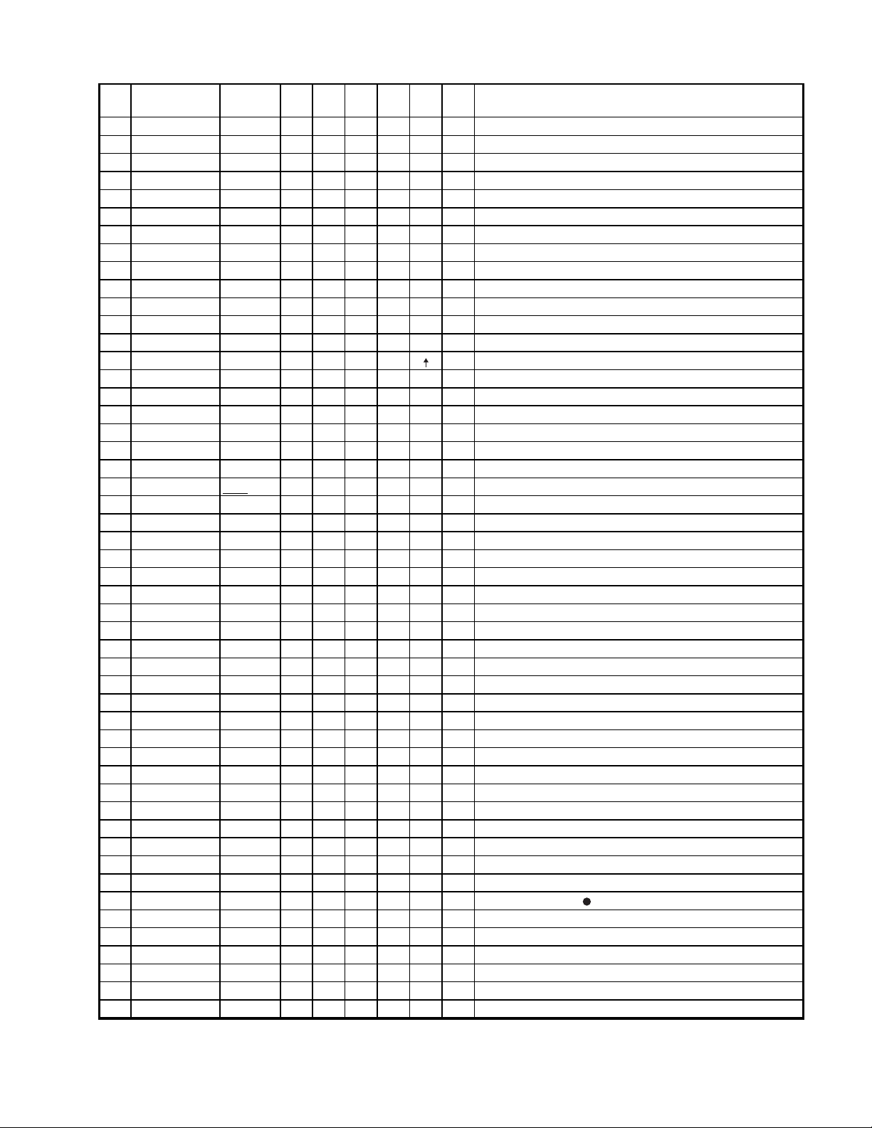
µPD78044FGF-188-3B9 Terminal Function
Pin
No.
Terminal Port I/O Typ Rst Ini Act Ext
64 63 62 61 60 59 58 57 56 55 54 53 52 51 50 49 48 47 46 45 44 43 42 41
65
66
67
68
69
70
71
72
73
74
75
76
77
78
79
80
123456789
P94/FIP6
P93/FIP5
P92/FIP4
PD78044FGF-188-3B9
10 11 12 13 14 15 16 17 18 19 20 21 22 23 24
DD
P90/FIP2
P81/FIP1
V
P80/FIP0
P27/SCK0
P26/SO0/SB1
P91/FIP3
P23/STB
P24/BUSY
P25/SIO/SBO
P21/SO1
P22/SCK1
REST
P20/SI1
P74
P73
AVss
Function
P17/AN17
P16/AN16
P15/AN15
40
39
38
37
36
35
34
33
32
31
30
29
28
27
26
25
P14/AN14
P33/TI1
P34/TI1
P35/PCL
P36/BUZ
P37
X2
X1
Vss
XT2
P04/XT1
AV
RES
AV
DD
P10/AN10
P11/AN11
P12/AN12
P13/AN13
1 P94/FIP6 NC O C Hz −−−Not used (Open)
2 P93/FIP5 6G O C Hz L H P. D VFD grid 6G (EMPHASIS, PLAY, PAUSE,REPEAT)
3 P92/FIP4 5G O C Hz L H P. D VFD grid 5G (11~20, A-B, PROG, )
4 P91/FIP3 4G O C Hz L H P. D VFD grid 4G (1~10)
5 P90/FIP2 3G O C Hz L H P. D VFD grid 3G (Seconds Digit, S, SINGLE)
6 P81/FIP1 2G O C Hz L H P. D VFD grid 2G (Minutes Digit, M, TOTAL)
7 P80/FIP0 1G O C Hz L H P. D VFD grid 1G (Track No., A.SPACE)
8VDD VDD −−−−−−Positive power (Connect to +5V)
9 P27/SCK0 MCK O B Hz H P. UP SM5841/PCM1735/BU2616 mode control clock output
10 P26/S00/SB1 MDT O B Hz −−P. UP SM5841/PCM1735/BU2616 mode control data output
11 P25/SI0/SB0 NC I B Hz −−P. DG Not used (Connect to GND)
12 P24/BUSY NC I B Hz −−P. DG Not used (Connect to GND)
13 P23/STB MLE O B Hz − P. UP SM5841/PCM1735 mode control latch output
14 P22/SCK1 CQCK O B Hz − − DSP, ASP Command clock & SUBQ readout clock output
15 P21/SO1 COIN O B Hz −−−DSP, ASP Command data output
16 P20/SI1 SUBQ I B Hz −−−DSP sub-code Q data input
17 RESET RESET I −−−L − Reset signal input
18 P74 NC I B Hz −−P. DG Not used (Connect to GND)
19 P73 XTAL O B Hz H L P. UP TC9246XTAL MODE change Lo:ON (Pitch 0),Hi:OFF(Variable pitch)
20 AVss AVss −−−−−−GND for A/D converter
21 P17/ANI7 DSP XRST O B Hz L L P. DG DSP reset signal output
22 P16/ANI6 DF XRST O B Hz L L P. DG Digital filter reset signal output
23 P15/ANI5 JOG B I B Hz −−P. UP Rotaly encoder JOG B input
24 P14/ANI4 JOG A I B Hz −−P. UP Rotaly encoder JOG A input
25 P13/ANI3 AD3 I B Hz − A P. UP Key data input 3 (A/D)
26 P12/ANI2 AD2 I B Hz − A P. UP Key data input 2 (A/D)
27 P11/ANI1 AD1 I B Hz − A P. UP Key data input 1 (A/D)
28 P10/ANI0 AD0 I B Hz − A P. UP Key data input 0 (A/D)
29 AVDD AV DD −−−−−−A/D converter analog power (Connect to +5V)
30 AVREF AVREF I −−−−−A/D converter Ref. V input (Connect to +5V)
Pin
No.
31 P04/XT1 NC I A −−−P. DG Not used (Connect to GND)
32 XT2 NC −−−−−−Not used (Open)
33 Vss GND −−−−−−GND
34 X1 X1 I A −−−−Main system clock input
35 X2 X2 −−−−−−Main system clock input
36 P37 MCS O B Hz H L P. DG PCM1735 chip select output
37 P36/BUZ MCE O B Hz L L − BU2616 chip enableoutput
38 P35/PCL RW C O B Hz L L − DSP read / write control output
39 P34/TI2 SL+ O B Hz L H − ASP sled drive signal output
40 P33/TI1 SL- O B Hz L H − ASP sled drive signal output
41 P32/T02 NC I B Hz −−P. DG Not used (Connect to GND)
42 P31/T01 CD/RW O B Hz H L P. DG CD / RW Gain change output
43 P30/T00 SEARCH O B Hz L H P. DG Servo control output at search
44 P03/INTP3/CI0 REMOCON I B Hz − − Remote control signal input
45 P02/INTP2 WRQ I B Hz L H − DSP SUBQ output standby input
46 P01/INTP1 DRF I B Hz L H − ASP DEFECT RF level detect input
47 P00/INTP0/TI0 NC I A Hz −−P. UP Not used (Connect to GND)
48 IC IC −−−−−−Connect to GND
49 P72 FSEQ I B Hz L H − DSP sync signal detect input
50 P71 A.MUTE O B Hz H H P. UP Analog mute output OFF: Lo, ON: Hi
51 P70 DRV.MUTE O B Hz H − P. UP MOTOR DRIVER MUTE control output Hi:Output ON
52 VDD VDD −−−−−−Positive power (Connect to +5V)
53 P127/FIP33 OPSW I C Hz − L P. UP Loader open position detect switch input
54 P126/FIP32 CLSW I C Hz − L P. UP Loader close position detect switch input
55 P125/FIP31 INSW I C Hz − L P. UP Pickup inner position detect switch input
56 P124/FIP30 OPEN O C Hz L H P. DG Loader open drive LA6559 signal output
57 P123/FIP29 CLOSE O C Hz L H P. DG Loader close drive LA6559 signal output
58 P122/FIP28 MODEL I C Hz −−−Model distinction input Lo:455, Hi:555
59 P121/FIP27 NC I C Hz −−P. DG Not used (Open)
60 P120/FIP26 NC I C Hz −−P. DG Not used (Open)
61 P117/FIP25 P1 O C Hz L H P. D VFD segment P1 (1a, 1, 11, EMPHASIS)
62 P116/FIP24 P2 O C Hz L H P. D VFD segment P2 (1b, 2, 12, PLAY)
63 P115/FIP23 P3 O C Hz L H P. D VFD segment P3 (1c, 3, 13, PAUSE)
64 P114/FIP22 P4 O C Hz L H P. D VFD segment P4 (1d, 4, 14, REPEAT)
65 P113/FIP21 P5 O C Hz L H P. D VFD segment P5 (1e, 5, 15)
66 P112/FIP20 P6 O C Hz L H P. D VFD segment P6 (1f, 6, 16)
67 P111/FIP19 P7 O C Hz L H P. D VFD segment P7 (1g, 7, 17)
68 P110/FIP18 P8 O C Hz L H P. D VFD segment P8 (2a, 8, 18)
69 P107/FIP17 P9 O C Hz L H P. D VFD segment P9 (2b, 9, 19)
70 P106/FIP16 P10 O C Hz L H P. D VFD segment P10 (2c, 10, 20)
71 VLOAD -HB I C −−−−Power for FL display (-HB)
72 P105/FIP15 P11 O C Hz L H P. D VFD segment P11 (2d, A-B)
73 P104/FIP14 P12 O C Hz L H P. D VFD segment P12 (2e, PROG)
74 P103/FIP13 P13 O C Hz L H P. D VFD segment P13 (2f, )
75 P102/FIP12 P14 O C Hz L H P. D VFD segment P14 (2g)
76 P101/FIP11 P15 O C Hz L H P. D VFD segment P15 (A.SPACE, TOTAL, SINGLE)
77 P100/FIP10 P16 O C Hz L H P. D VFD segment P16 (M, S)
78 P97/FIP9 NC O C Hz −−−Open (Not used)
79 P96/FIP8 NC O C Hz −−−Open (Not used)
80 P95/FIP7 NC O C Hz −−−Open (Not used)
Type A: Standard input port Note) P.D: Pull−down to VDISP
Terminal Port I/O Typ Rst Ini Act Ext Function
B: Standard in/output port P.DG: Pull−down to GND
C: Hi−voltage proof in/output port
D: P−ch open drain hi−voltage proof
13
D
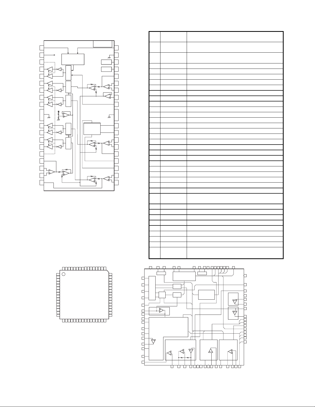
LA6559 (IC101)
1
REV
Signal System VCC
2
S-VCC
VCC2
VLO-
VLO+
VO4+
VO4-
VO3+
VO3-
VO2+
VO2-
VO1+
VO1-
VCC1
VIN1
VIN1-
VIN1+
VIN2
FR
3
4
5
6
7
8
9
Power
System
GND
FR
10
11
12
13
14
15
16
17
18
Power Supply
(LOADING)
Power Supply
(CH1 to CH4)
(Forward/Reverse/
Break/OFF)
Control
Shift
Shift
Shift
Shift
33k
11k
LA9241M (IC103)
Input
Output
Level
Level
Level
Level
Signal System GND
CH2 to CH4
Output
CH1 Output
ON/OFF
33k
Power System GND
3.3VREG
(External PNP)
33k
3.3VREG GND
3.3VREG
Power Supply
33k
Thermal
Shutdown
MUTE2
MUTE1
11k
PNP Tr
Collector
PNP Tr
11k
11k
Base
FWD
36
S-GND
35
MUTE2
34
33
MUTE1
32
VIN4
31
VIN4-
30
VIN4+
29
VREF-IN
28
VCONT(LOADING)
FR
FR
27
REG-OUT
26
REG-IN
25
VIN3+
24
VIN3-
23
VIN3
22
GND-VREG
21
VCC-VREG
20
VIN2+
19
VIN2-
Pin
No.
Name
1 REV
2 S-Vcc
Function
5CH output change terminal, logic input of
loading block
signal system power supply
(BTL-AMP:CH1~4)
3 Vcc2 Power supply for loading block
4VL0− Loading output (−)
5 VL0+ Loading output (+)
6 VO4+ Output terminal (+) for channel 4
7 VO4− Output terminal (−) for channel 4
8 VO3+ Output terminal (+) for channel 3
9 VO3− Output terminal (−) for channel 3
10 VO2+ Output terminal (+) for channel 2
11 VO2− Output terminal (−) for channel 2
12 VO1+ Output terminal (+) for channel 1
13 VO1− Output terminal (−) for channel 1
14 Vcc1 CH1•`CH4(BTL-AMP) output stage power supply
15 VIN1 Input terminal for channel 1
16 VIN1− OP-AMP input AMP-A input terminal (−)
17 VIN1+ OP-AMP input AMP-A input terminal (+)
18 VIN2 Input terminal for channel 2, input AMP output
19 VIN2− Input terminal (−) for channel 2
20 VIN2+ Input terminal (+) for channel 2
21 Vcc-VREG 3.3VREG power supply
22 GND-VREG 3.3VREG GND
23 VIN3 Input terminal for channel 3, input AMP output
24 VIN3− Input terminal (−) for channel 3
25 VIN3+ Input terminal (+) for channel 3
26 REG-IN PNP transistor base connected
27 REG-OUT
3.3V power output to which the PNP transistor
collector connected
28 VCONT Loading output voltage set terminal
29 VREF-IN Reference voltage applied terminal
30 VIN4+ Input terminal (+) for channel 4
31 VIN4- Input terminal (−) for channel 4
32 VIN4 Input terminal for channel 4, input AMP output
33 MUTE1 Output ON/OFF for channel 1 (BTL AMP)
34 MUTE2 Output ON/OFF for channel 2 to 4 (BTL AMP)
35 S-GND Signal system GND
36 FWD
Output change terminal (FWD) for loading
output (VLO+−), logic input of loading block
14
VCC1
LDS
LDD
BH1
646362616059585756555453525150
FIN2
1
FIN1
2
E
3
F
4
TB
5
-
TE
6
TE
7
TESI
8
SCI
9
TH
10
TA
11
-
TD
12
TD
13
JP
14
TO
15
FD
16
171819202122232425262728293031
-
FAFAFE
FD
VCC1
LDS
LDD
BH1
PH1
LF2VRREFI
VCC2
FSS
SPINDLE
SERVO
NC
-com
SP
SP
SPG
DRFCEDATCLCLK
SPD
PH1
LF2
VR
REFI
VCC2
FSS
DRFCEDATCLCLK
DEF
49
48
NC
47
TBC
46
FSC
45
DGND
44
SLI
43
SLC
-
42
RFS
41
RFSM
+
40
CV
-
39
CV
38
SLOF
37
HFL
36
TES
35
TOFF
34
TGL
+
33
JP
-
-
SP
NC
FE
SP
SPG
AGND
32
-
-
+
JP
SL
SL
SLD
SPD
SLEQ
FIN2
FIN1
TESI
1
2
3
E
4
F
5
TB
6
TE
TE
7
8
9
SCI
10
TH
TA
11
-
TD
12
TD
13
JP
14
TO
15
FD
16
APC
I/V
TE
T. SERVO & T.LOGIC
RF DET
VCA
VCABAL
F.SERVO & F.LOGIC
17 18 19 20 21 22 23 24 25 26 27 28 29 30 31 32
FAFAFE
FD
REF
INTER FACE
-
FE
GND
SLC
RF Amp
SLED SERVO
SLD
SLEQ
DEF
49505152535455565758596061626364
NC
48
47
TBC
FSC
46
45
DGN
SLI
44
SLC
43
-
42
RFS
RFSM
41
+
CV
40
-
CV
39
SLOF
38
37
HFL
TES
36
TOFF
35
TGL
34
+
JP
33
-
-
+
SL
JP
SL
 Loading...