Denon DCD-1650SR Service Manual
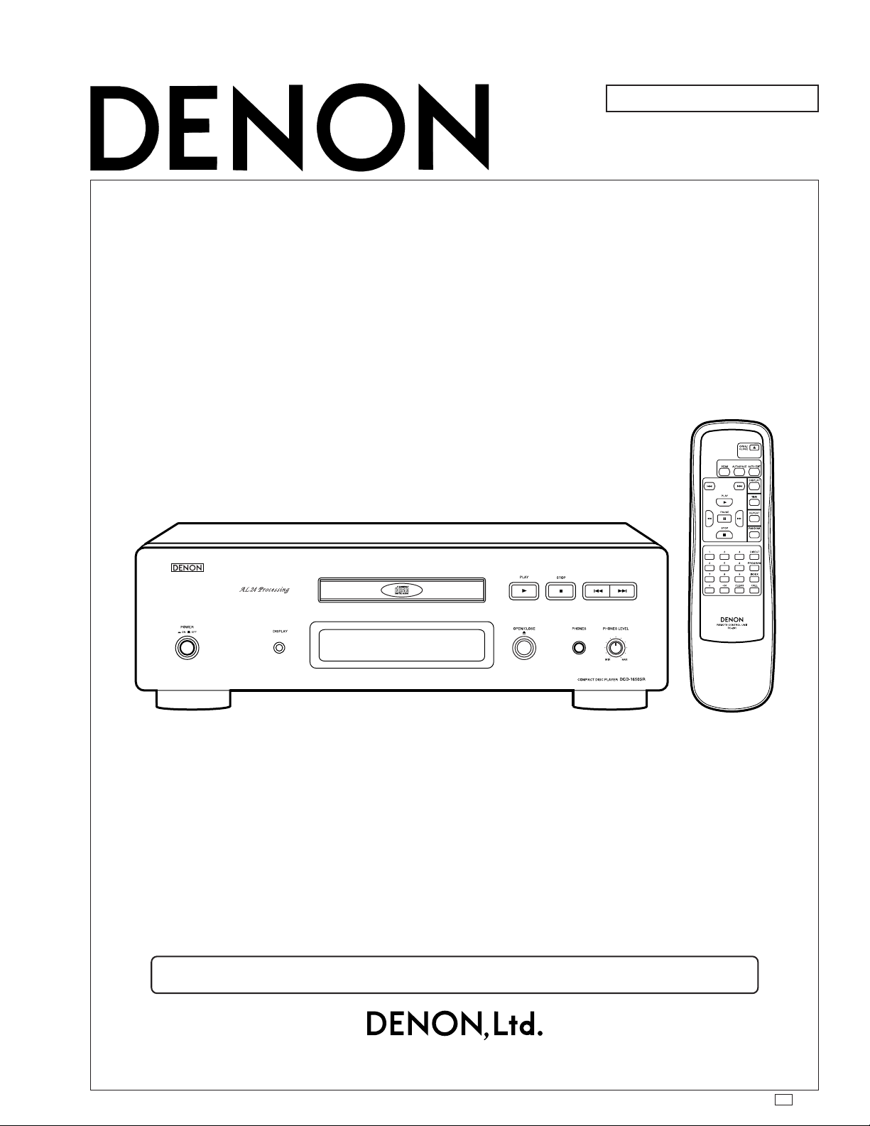
SERVICE MANUAL
For Asia & China model
Hi-Fi Component
MODEL
DCD-1650SR
STEREO CD PLAYER
Some illustrations using in this service manual are slightly different from the actual set.
16-11, YUSHIMA 3-CHOME, BUNKYOU-KU, TOKYO 113-0034 JAPAN
Telephone: 03 (3837) 5321
X0140 NC 0204

DCD-1650SR
SAFETY PRECAUTIONS
The following check should be performed for the continued protection of the customer and service technician.
LEAKAGE CURRENT CHECK
Before returning the unit to the customer, make sure you make either (1) a leakage current check or (2) a line to chassis
resistance check. If the leakage current exceeds 0.5 milliamps, or if the resistance from chassis to either side of the
power cord is less than 460 kohms, the unit is defective.
SPECIFICATIONS
AUDIO
No. of Channels: 2 channels
Frequency Response: 2~20,000 Hz
Dynamic Range: 100 dB
Signal-to-noise Ratio: 118 dB
Harmonic Distortion: 0.0018 % (1 kHz)
Separation: 110 dB (1 kHz)
Wow & Flutter: Below measurable limit:
(±0.001 % W.peak)
Output Voltage: FIXED 2.0 V
DISCS CD-DA (Compact Disc-Digital Audio) format
CD-R/RW Disc for Audio consumer use
GENERAL CHARACTERISTICS
Power Supply: 230 V/50 Hz
Power Consumption: 17 W
Dimensions: 434 (W) × 135 (H) × 340 (D) mm
Mass: 12.7 kg
REMOTE CONTROL UNIT RC-281
Remote Control System: Infrared pulse system
Power Supply: 3 V DC; two R6P (standard size AA)
dry cell batteries
External Dimensions: 68 (W) × 233 (H) × 20 (D) mm
Mass: 160 g (including batteries)
2
DISASSEMBLY
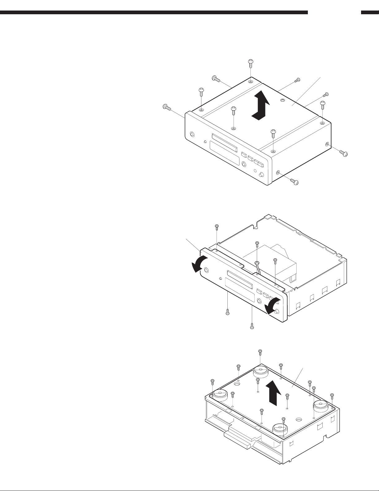
(To reassemble reverse disassembly)
1. Top Cover
1. Remove 2 screws from rear side and 4 screws from both sides,
then remove 5 upper screws.
2. Detach the Top Cover as shown in the arrow direction.
DCD-1650SR
Top Cover
2. Front Panel
1. Remove 3 upper screws, 2 below screws and 1P Contact.
2. Detach the Front Panel as shown in the figure.
Front Panel
3. Bottom Cover
1. Remove 12 screws from bottom side.
2. Detach the Bottom Cover as shown in the arrow direction.
Bottom Cover
3
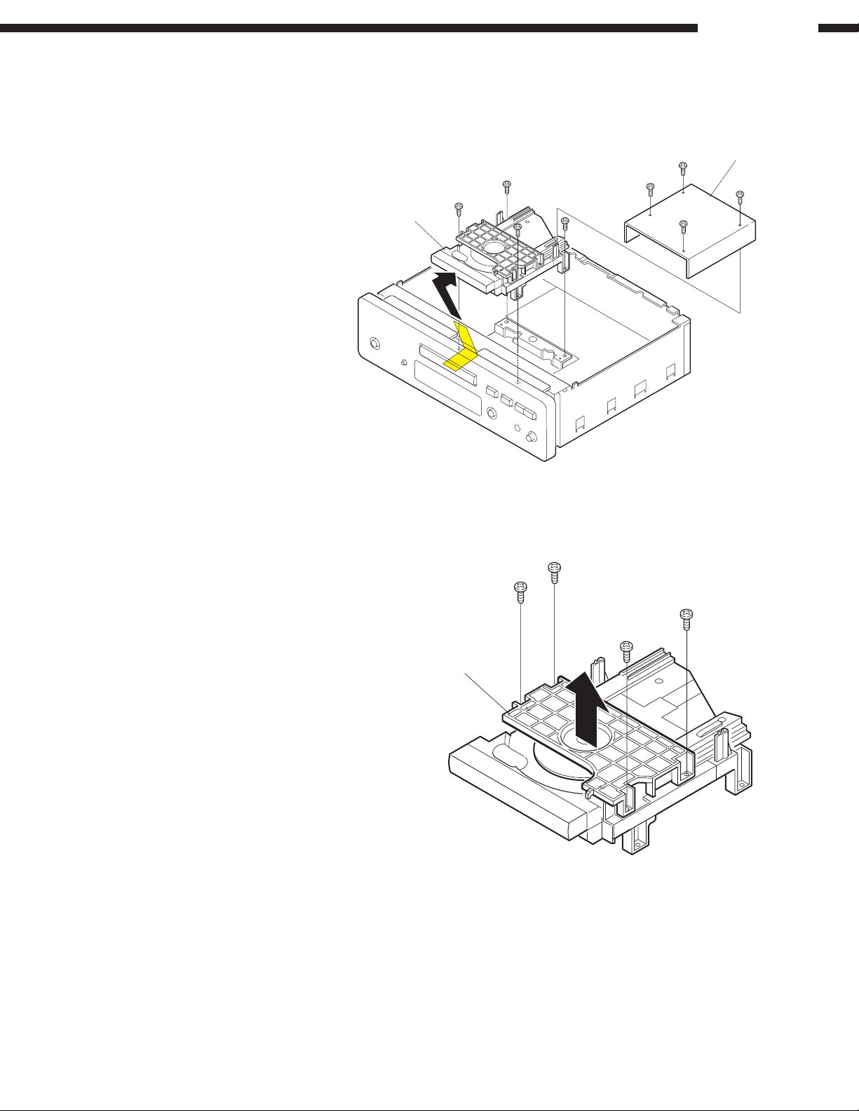
4. Mechanism Unit
1. Remove 4 screws fixing the Mechanism Cover and detach the Mechanism
Cover as shown in the arrow direction.
2. Remove 4 screws fixing the Mechanism Unit, then detach the Mechanism
Unit as shown in the figure.
Mechanism Unit
DCD-1650SR
Mechanism Cover
5. Clamper
1. Remove 4 screws fixing the Clamper.
2. Detach the Clamper as shown in the arrow direction.
Clamper
Caution Before Disassembling Power Trans. & Power P.W.B. Unit
Be sure to disconnect AC Inlet from the rear panel before disconnecting 3P connector cord of the Power Trans. from CN035
connector base on the Power P.W.B. Unit.
4
DCD-1650SR
NOTE IN HANDLING FOR LASER PICK-UP
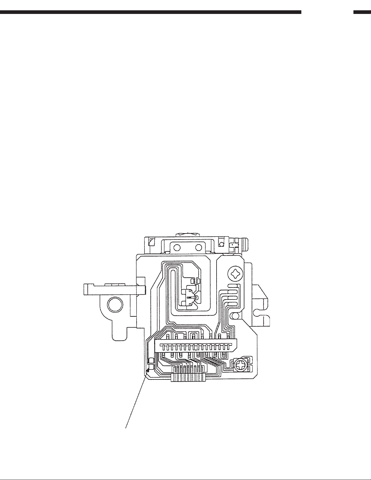
1. Protection of the LD
Short a part of the LD circuit by soldering. After connection to a circuit, remove the short solder.
2. Precautions when handling the CD mechanism
Handle the laser pick-up so that it is not exposed to dust.
Do not leave the laser pick-up bare. Be sure to cover it.
If dust adheres on lens of the pick-up, blow it off with a blower brush.
Do not shock the laser pick-up.
Do not watch the light of the laser pick-up.
3. Cautions on assembling and adjustment
Be sure that to the bench, jig, head of soldering (with ceramic) iron and measuring instruments are well grounded.
Workers who handle the laser pick-up must be grounded.
The finished mechanism (prior to anchoring in the set) should be protected against static electricity and dust.
The mechanism must be stored so that damaging outside forces are not received.
When carrying the finished mechanism, hold it by the chassis body.
For proper operation, storage and operating environment should not contain corrosive gases. For example H
NO2, CL2 etc. In addition storage environment should not have materials that emit corrosive gases especially from
silicic, cyanic, formailn and phenol group. In the mechanism or the set, existence of corrosive gases may cause no
rotation in motor.
2S, SO2
4. Location to shorting PAD
SF-P101NXR
Protective soldering place for laser diode.
(Remove before APC circuit power on, while conneting the connector)
5
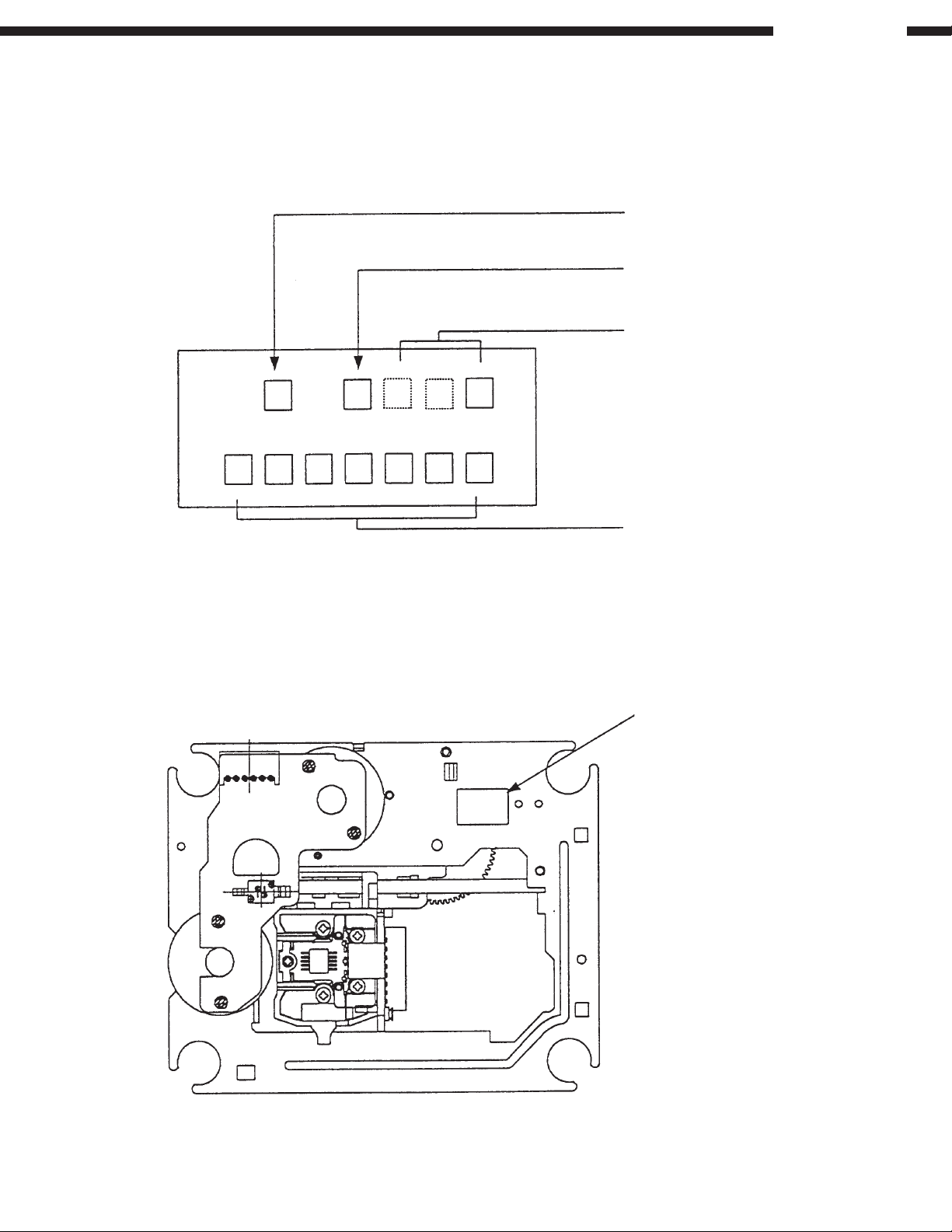
5. Serial number formation
Serial number label
DCD-1650SR
Factory number
CD mechanism ass’y number
Production process line number
(1, 2, or 3 digits)
Manufacturing number
Serial number label
6
CD TEST MODE
g
g
y
y
Setting of the test mode
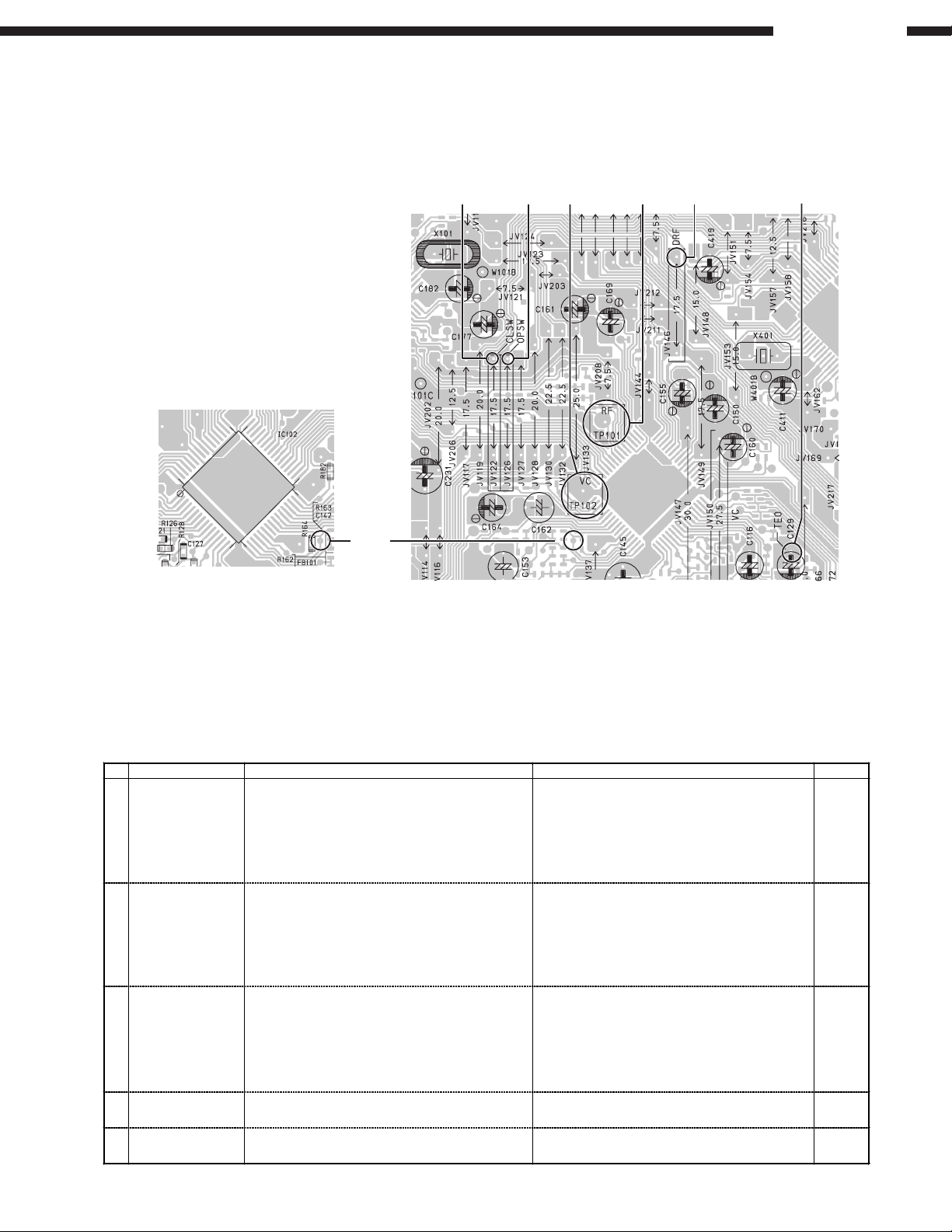
How to start the test mode: Turn on the power in the condition that CLSW (Test Point)
and OPSW (Test Point ) are being shorted. ( “01” is indicated on the DISPLAY)
To exit from the test mode, turn off the power. (Refer to Fig. 1 “Test Point Layout”)
CLSW OPSW RFVC DRF TEO
DCD-1650SR
FEO
(Foil Side)
Fig. 1 “Test Point” Layout
* Laser light of the pickup is always emitted regardless of DISC loading in the test mode.
You may lose your eyesight if you look into the laser directly.
So be careful enough when operating in the test mode.
Used DISC: A-BEX TCD784
Explanation of each button
* Use only the buttons described below for operations while in the test mode, and don’t push any other buttons.
No Name of button Function Display Note
Simultaneous
1
turn-on of Mecha.
OPEN and CLOSE
SW
Pressing
2
OPEN/CLOSE button
Pressin
3
4
5
PLAY button Focus/Tracking check mode
Pressing MANUAL
SEARCH REV or
FWD button
Pressing
PAUSE button
Mode activation
1. This mode starts.
2. Slide moves to the initial setting position
(10mm from inner circle).
3. To cancel this mode, turn off the power and on a
4. Other key input used other than this mode is not
guaranteed. (it may become abnormal operation).
Disc loading mode
1. Loader opens by OPEN/CLOSE input.
2. Disc chucking is made when closing the loader
with OPEN/CLOSE key after setting a disc.
3. Slide moves to the initial setting position
(10mm from inner circle).
4. It stops at the status 3.
1. Laser turns on when PLAY is pushed once
(servo stop status).
2. It performs Focus search when PLAY is pushed
Again, and Focus servo is turned on (disc rotation,
Tracking off). If no disc, it stops after retry. It repeats
Focus search if the button is kept depressed.
3. Tracking servo/Slide servo turns on when PLAY is
pushed once more, and CLV is locked.
Pickup move mode
Pickup moves to REV or FWD direction when the
button is pushed at stop status.
Auto adjust mode
It performs auto adjust mode. 1. “06” is indicated on the TRACK No. display, and
1. To show now in this mode, “01” is indicated on the
TRACK No. display.
ain.
1. “01” is indicated continuously.
1. “02” is indicated on the TRACK No. displa
on the TIME display.
2. “03” is indicated on the TRACK No. display, and
“F on” on the TIME display.
3. “04” is indicated on the TRACK No. displa
on the TIME display.
1. “05” is indicated on the TRACK No. display, and
“O PU” on the TIME display.
“A dJ” on the TIME display.
, and “L on”
, and “t on”
Mute on
7
How to check the test mode
( 1 ) DISC discrimination, adjustment
* Insert DISC, and press the PAUSE button on the Remote Control Unit.
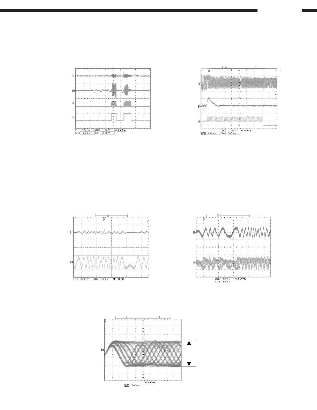
* “06 Adj” is displayed, and discrimination of DISC size 8 cm/12 cm, discrimination of DISC reflectance (CD, CD-
R/CD-RW), adjustment of focus, tracking offset, and EF balance will be performed. (Adjusted values are not
displayed: Refer to Fig. 2, 3)
DCD-1650SR
FEO
TEO
RF
FEO
TB
SLD
DRF
Fig. 2 DISC discrimination,
Fig. 3 Adjustment of EF balance
adjustment (Case of CD-RW)
* After completing the discrimination and adjustment, it becomes stop condition.
* Once discrimination of DISC has been carried out in the “06 Adj” mode, discrimination of size and reflectance is
no longer made, and only adjustment will be performed.
( 2 ) Checking of servo state
* Press the PLAY button after performing above (1) “DISC discrimination, adjustment”.
* “02 L on” is displayed, and the laser will start to light. (The pickup may vibrate with a rattling noise if DISC has
been loaded, but this is not abnormal.)
* Press the PLAY button again.
* “03 F on” is displayed. DISC starts turning, and focus servo will be actuated. (Refer to Fig. 4, 5)
FEO
TEO
TEO
RF
Fig. 4 In “03 F on” Fig. 5 In “03 F on”
* Press the PLAY button again.
* “04 t on” is displayed. Tracking, CLV, and slide servo will be actuated.
* Monitor RF signal using the Test Point, RF point and VC point.
Check that the signal’s amplitude is 1.5V±0.3Vp-p. (Refer to Fig. 6)
RF
A (A=1.5r0.3Vp-p)
Fig. 6 In “04 t on”
8
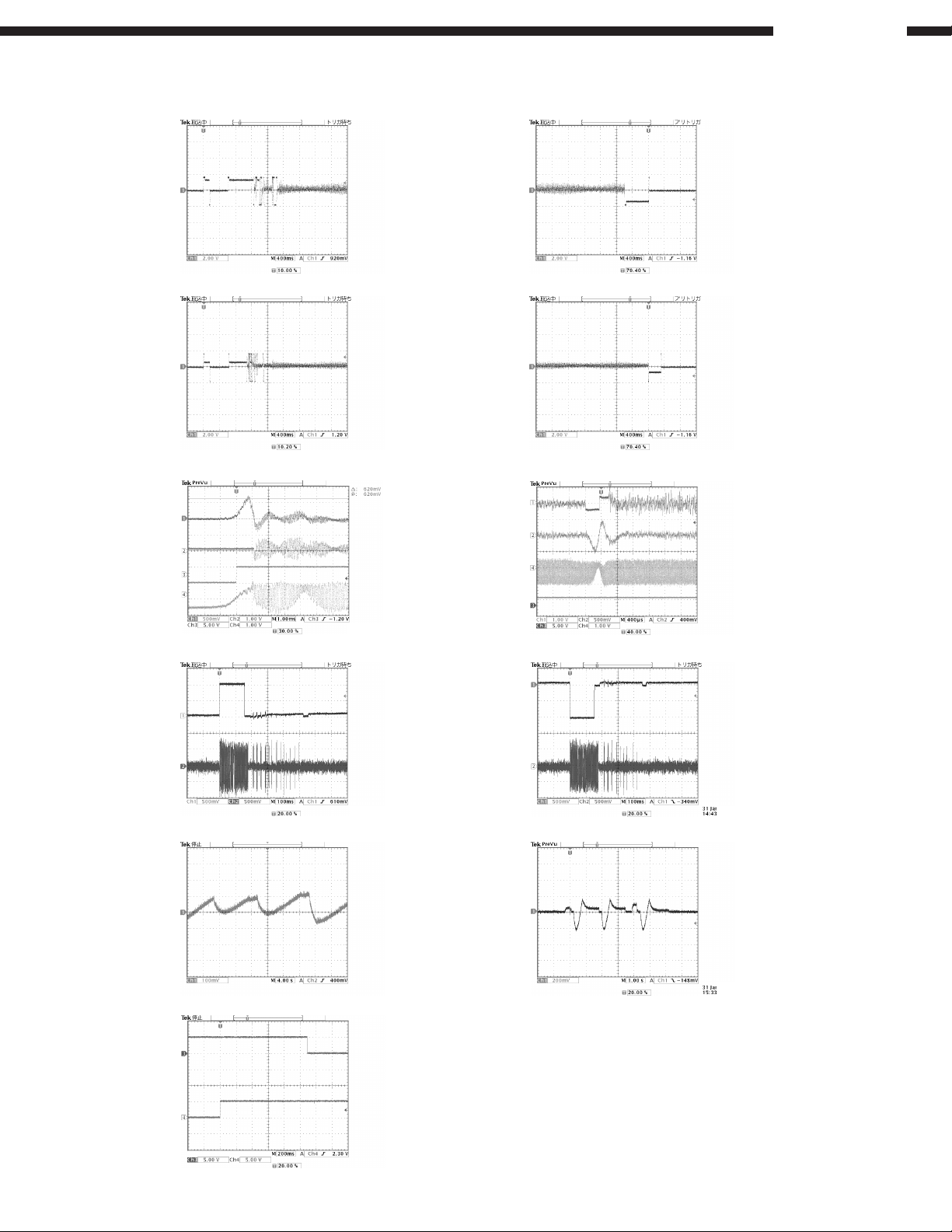
WAVE-FORMS OF EACH POINT
DCD-1650SR
SPD
SPD
FEO
TEO
DRF
RF
When 12 cm DISC
start
When 8 cm DISC
start
When focus
servo on
SPD
SPD
TD
TEO
RF
DRF
When 12 cm DISC
stop
When 8 cm DISC
stop
During PAUSE
SLD
TEO
SLD
OPEN
CLOSE
Track search
(when forward)
During PLAY
When the tray
OPEN
SLD
TEO
FD
Track search
(when reverse)
Focus search
(no DISC)
9
0
SEMICONDUCTORS
IC’s
µµ
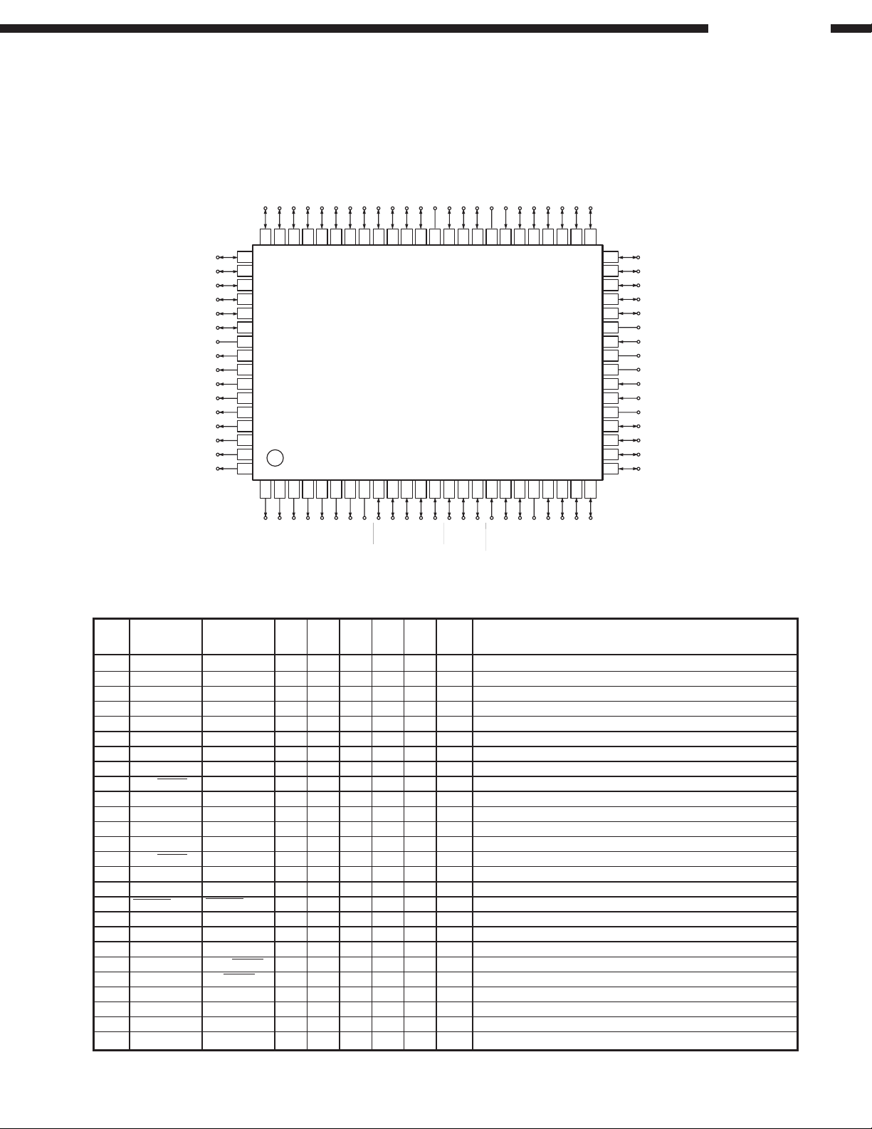
µPD78044*** (IC402)
µµ
P114/FIP22
64 63 62 61 60 59 58 57 56 55 54 53 52 51 50 49 48 47 46 45 44 43 42 41
P113/FIP21
P112/FIP20
P111/FIP19
P110/FIP18
P107/FIP17
P106/FIP16
V
LOAD
P105/FIP15
P104/FIP14
P103/FIP13
P102/FIP12
P101/FIP11
P100/FIP10
P97/FIP9
P96/FIP8
P95/FIP7
65
66
67
68
69
70
71
72
73
74
75
76
77
78
79
80
123456789
DCD-1650SR
P115/FIP23
P116/FIP24
P117/FIP25
P120/FIP26
P121/FIP27
P122/FIP28
P123/FIP29
P124/FIP30
P125/FIP31
P126/FIP32
P127/FIP33
VDDP70
P71
P72
IC (Vpp)
PO0/INTP0/T1
PO1/INTP1
PO2/INTP2
P03/INTP3/C10
P30/TO0
P31/TO1
P32/TO2
40
P33/TI1
39
P34/TI1
38
P35/PCL
37
P36/BUZ
36
P37
35
X2
34
X1
33
Top View
10 11 12 13 14 15 16 17 18 19 20 21 22 23 24
Vss
32
XT2
31
P04/XT1
30
AV
29
28
27
26
25
REF
AV
DD
P10/ANI0
P11/ANI1
P12/ANI2
P13/ANI3
DD
P94/FIP6
P93/FIP5
µµ
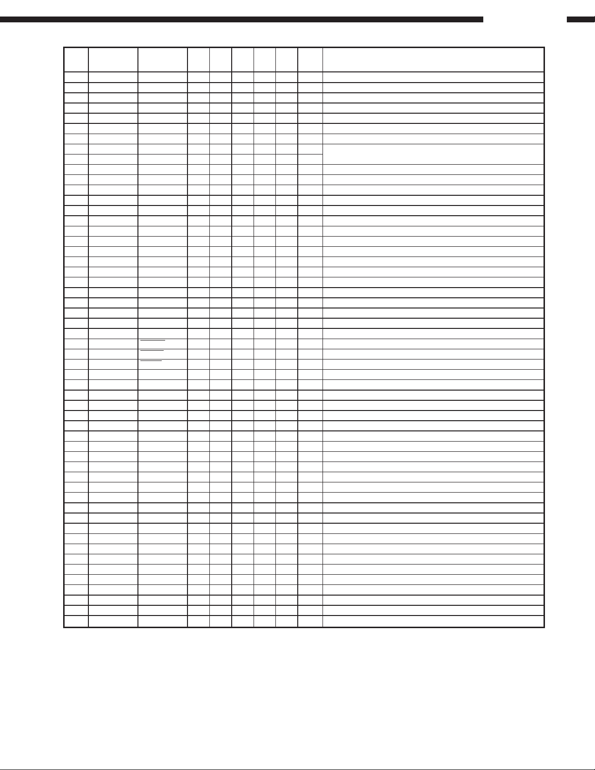
µPD78044*** Terminal Function
µµ
Pin
Pin Name FunctionI/OPort Typ Rst Ini Act Ext
No.
P92/FIP4
P91/FIP3
P90/FIP2
P81/FIP1
V
P80/FIP0
P27/SCK0
26/SO0/SB1
P24/BUSY
P25/SI0/SBO
P23/STB
P22/SCK1
P20/SI1
P21/SO1
P74
P73
AVss
RESET
P17/ANI7
P16/ANI6
P15/ANI5
P14/ANI4
1 P94/FIP6 4G O C HZ L H P.D VFD grid 4G
2 P93/FIP5 5G O C HZ L H P.D VFD grid 5G
3 P92/FIP4 6G O C HZ L H P.D VFD grid 6G
4 P91/FIP3 7G O C HZ L H P.D VFD grid 7G
5 P90/FIP2 8G O C HZ L H P.D VFD grid 8G
6 P81/FIP1 9G O C HZ L H P.D VFD grid 9G
7 P80/FIP0 10G O C HZ L H P.D VFD grid 10G
8VDD VDD Positive power (connect to +5V)
9 P27/SCK0 MCK O B HZ H ↑ P.UP DXP6001AF mode control clock
10
P26/SO0/SB1
MDT O B HZ P.UP DXP6001AF mode control data
11 P25/SI0/SB0 NC I B HZ P.DG Not used (connect to GND)
12 P24/BUSY NC I B HZ P.DG Not used (connect to GND)
13 P23/STB MLE O B HZ ↑P.UP DXP6001AF mode control latch
14 P22/SCK1 CQCK O B HZ H ↑DSP, ASP command clock and SUBQ taking clock output
15 P21/SO1 COIN O B HZ DSP, ASP command data output
16 P20/SI1 SUBQ I B HZ DSP sub-code Q data input
17 RESET RESET I L Reset signal input
18 P74 NC I B HZ P.DG Not used (connect to GND)
19 P73 NC I B HZ P.DG Not used (connect to GND)
20 AVSS AVSS GND for A/D converter
21 P17/ANI7 DSP XRST O B HZ L L P.DG DSP reset signal output
22 P16/ANI6 DF XRST O B HZ L L P.DG Digital filter reset signal output
23 P15/ANI5 NC I B HZ P.DG Not used (connect to GND)
24 P14/ANI4 NC I B HZ P.DG Not used (connect to GND)
25 P13/ANI3 AD3 I B HZ A P.UP Key data input 3 (A/D)
26 P12/ANI2 AD2 I B HZ A P.UP Key data input 2 (A/D)
10
DCD-1650SR
Pin
Pin Name FunctionI/OPort Typ Rst Ini Act
No.
27 P11/ANI1 AD1 I B HZ A P.UP Key data input 1 (A/D)
28 P10/ANI0 AD0 I B HZ A P.UP Key data input 0 (A/D)
29 AVDD AVDD Analog power for A/D converter (connect to +5V)
30 AVREF AVREF I Ref. V input for A/D converter (connect to +5V)
31 P04/XT1 NC I A P.DG Not used (connect to GND)
32 XT2 NC Not used (open)
33 VSS GND GND
34 X1 X1 I A
35 X2 X2
36 P37 NC O B HZ L Not used (open)
37 P36/BUZ NC O B HZ L Not used (open)
38 P35/PCL RWC O B HZ L L DSP read/write control output
39 P34/TI2 SL+ O B HZ L H ASP sled forward signal output
40 P33/TI1 SL- O B HZ L H ASP sled forward signal output
41 P32/TO2 NC I B HZ P.DG Not used (connect to GND)
42 P31/TO1 CD/RW O B HZ H L P.DG CD-RW gain switching output
43 P30/TO0 SEARCH O B HZ L H P.DG Servo control output while search
44
P03/INTP3/CI0
45 P02/INTP2 WRQ I B HZ L H DSP SUBQ output standby input
46 P01/INTP1 DRF I B HZ L H ASP DEFECT RF level detect output
47
P00/INTP0/TI0
48 IC IC Connect to GND
49 P72 FSEQ I B HZ L H DSP sync. signal detect input
50 P71 A.MUTE O B HZ H H P.UP Analog mute output, L: OFF, H: ON
51 P70 DRV.MUTE O B HZ H P.UP Motor drive mute control output, H: Output ON
52 VDD VDD Positive power (connect to +5V)
53 P127/FIP33 OPSW I C HZ L P.UP Loader open position detect switch input
54 P126/FIP32 CLSW I C HZ L P.UP Loader close position detect switch input
55 P125/FIP31 INSW I C HZ L P.UP Pickup inner circle position detect switch input
56 P124/FIP30 OPEN O C HZ L H P.DG Loader open drive (BA15218) signal output
57 P123/FIP29 CLOSE O C HZ L H P.DG Loader close drive (BA15218) signal output
58 P122/FIP28 NC O C HZ Not used (open)
59 P121/FIP27 NC O C HZ Not used (open)
60 P120/FIP26 NC O C HZ Not used (open)
61 P117/FIP25 NC O C HZ Not used (open)
62 P116/FIP24 NC O C HZ Not used (open)
63 P115/FIP23 NC O C HZ Not used (open)
64 P114/FIP22 NC O C HZ Not used (open)
65 P113/FIP21 S1 O C HZ L H P.D VFD segment S1
66 P112/FIP20 S2 O C HZ L H P.D VFD segment S2
67 P111/FIP19 S3 O C HZ L H P.D VFD segment S3
68 P110/FIP18 S4 O C HZ L H P.D VFD segment S4
69 P107/FIP17 S5 O C HZ L H P.D VFD segment S5
70 P106/FIP16 S6 O C HZ L H P.D VFD segment S6
71 VLOAD -HB I C Power for FLT (-HB)
72 P105/FIP15 S7 O C HZ L H P.D VFD segment S7
73 P104/FIP14 S8 O C HZ L H P.D VFD segment S8
74 P103/FIP13 S9 O C HZ L H P.D VFD segment S9
75 P102/FIP12 S10 O C HZ L H P.D VFD segment S10
76 P101/FIP11 S11 O C HZ L H P.D VFD segment S11
77 P100/FIP10 S12 O C HZ L H P.D VFD segment S12
78 P97/FIP9 1G O C HZ L H P.D VFD grid 1G
79 P96/FIP8 2G O C HZ L H P.D VFD grid 2G
80 P95/FIP7 3G O C HZ L H P.D VFD grid 3G
REMOCON I B HZ ↑P.UP Remote control input
NC I A HZ P.DG Not used (connect to GND)
Ext
Main system clock input
Type A: Standard input port Note) P.D: Pull-down to VDISP
B: Standard in/output port P.DG: Pull-down to GND
C: Hi-voltage proof in/output port
D: P-ch open drain hi-voltage
11
DXP6001AF (IC201)
4
33
DCD-1650SR
23
34
4
1
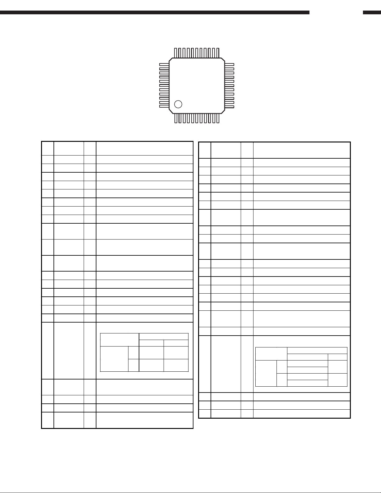
DXP6001AF Terminal Function
Pin
Pin Name I/O Descrption
No.
1 MDT Ip Microcomputer Interface Data
2 MCK Ip Microcomputer Interface Clock
3 MLEN Ip Microcomputer Interface Latch Enable
4 RSTN Ip Reset Terminal
5 DLRCK Ip Audio Serial Input Data L/R Clock
6 VSS Ground Terminal
7 DBCK Ip Audio Serial Input Bit Clock
8 DDT Ip Audio Serial Input Data
9 TEST2N Ip
10 TEST3N Ip
11 TEST4N Ip
12 DFBCK Ip Lambda-processor Input Bit Clock
13 DFWCK Ip Lambda-processor Input Word Clock
14 DOL Ip Lambda-processor Input Data L-channel
15 DOR Ip Lambda-processor Input Data R-channel
16 LMOD Ip Lambda-processor Operation Mode Set
17 OMOD1 Ip Output Mode Setting Terminal 1
18 OMOD2 Ip
19 INVIN Ip
20 BCKO O Lambda-processor Output Bit Clock
21 WCKO O Lambda-processor Output Word Clock
22 WCKO2 O
Test Setting Terminal 2 (Alpha-processor 1
Output shifts 12-bit.)
Test Setting Terminal 3 (Alpha-processor 2
Output stops.)
Test Setting Terminal 4 (Lambda-processor
Output stops.)
Output Mode Setting Terminal 2
OMOD1
LH
OMOD2
L
H
18bit
Alternate
20bit
Parallel
24bit
Alternate
24bit
Parallel
Lambda-processor Input Reversed
Polarity Terminal
Lambda-processor Output Word Clock 2
(for Canceling OFFSET on 1DAC
22
12
11
Pin
Pin Name I/O Descrption
No.
23P24L O/Lambda-processor Lch 24th bit Output *1, *2
24P23L O/Lambda-processor Lch 23rd bit Output *1, *2
25P22L O/Lambda-processor Lch 22nd bit Output *1, *2
26P21L O/Lambda-processor Lch 21st bit Output *1
27P20L O/Lambda-processor Lch 20th bit Output *1
28 VDD Power Supply Terminal
29 SO2L/P19L O
Lambda-processor Lch() Output /19
Output *1
30 SO1L O Lambda-processor Lch(+) Output
31 SO1R O Lambda-processor Rch(+) Output
32 SO2R/P19R O
Lambda-processor Rch() Output/19
Output *1
33P20R O/Lambda-processor Rch 20th bit Output *1
34P21R O/Lambda-processor Rch 21st bit Output *1, *2
35P22R O/Lambda-processor Rch 22nd bit Output *1, *2
36P23R O/Lambda-processor Rch 23rd bit Output *1, *2
37P24R O/Lambda-processor Rch 24th bit Output *1, *2
38 TEST1N Ip Test Terminal 1 (Alpha-processor 1 stops)
39 CKSLN Ip System Clock Select (384fs system /
256fs system)
40 CKDV1 Ip System Clock Divider Select Terminal 1
System Clock Divider Select Terminal 2
CKDV1
LH
41 CKDV2 Ip
CKDV2
192fs (CKSLN=H)
L
256fs (CKSLN=H)
192fs (CKSLN=H)
H
256fs (CKSLN=H)
42 XTI I X-TAL Oscillator Input Terminal
43 XTO O X-TAL Oscillator Output Terminal
44 CKO O Clock Output Terminal
th
th
768fs
384fs
bit
bit
(Ip = Input Terminal with pull-up)
*1: Outputted on OMOD1=L (18-bit Alternate Output or 20
*2: Internal Signal is outputted on OMOD1=H (24-bit Alternate Output or 24
-
bit Parallel Output)
-
bit Parallel Output) and one of TEST1N, TEST2N, TEST3N
or TEST4N is set to L.
12
Synchronization
detection
EFM Demodulation
Slice Level
Control
CLV
Digital servo
Subcode
separation
Q CRC
Microprocessor
Interface
VCO
oscillator
Clock control
2k
´
8-bit
RAM
RAM address
generator
C1 and C2 error
detection and correction
Flag processing
General-purpose
ports/Anti-shock
interface
8´ oversampling
digital filters
One-bit D/A
converter
Crystal oscillator system
Timing generator
DEFI
EFMIN
FSEQ
CLV+
CLV-
V/P
SFSY
CS
WRQ
SQOUT
CQCK
CO IN
RWC
FST
FOCS
FZD
TOFF
JP-
JP+
THLD
TGL
EMPH
EFLG
16M
4.2M
CK2
FSX
XV
SS
XOUT
XIN
XV
DD
RV
DD
MUTER
RCHP
RCHN
LCHN
LCHP
LV
SS
MUTEL
LRCKO
DFORO
DFOLO
DACKO
DOUT
ROMXA
C2F
LRSY
V
SSVDD
TEST3
TEST4
TEST5
TEST1
TEST2
TAI
PCK
FR
ISET
PDO
VV
SSVVDD
EFMO
TST11
PW
SBCK
SBSY
DEMO
EFMO
TST10
Level meter
Peak meter
Interpolation
and mute
Bilingual function (1)
Digital output
Bilingual function (2)
Digital
attenuator
ASDACK/P0
ASDFIN/P1
ASDEPC/P2
ASLRCK/P3
LV
DD
HFL
TES
Servo
commander
RES
LASER
CONT
RV
SS
SQOUT
CO IN
ASDEPC/P2
ASDFIN/P1
ASDACK/P0
TST10
DACKO
DFOLO
DFORO
LRCKO
1
23
4567
8
9
10
11
12 13
14
15 16
17 18 19 20
21
22
23 24
4142
43
44
45
46
47
48
49
50
5152
53
54
55
56
57
58
59
6061
626364
RWC
WRQ
FSX
SBCK
SFSYPWEFLG
SBSY
DOUT
MUTER
RVDDRCHP
RCHN
RVSSLVSSLCHN
LCHP
LVDDMUTEL
C2F
ROMXA
CK2
LRSY
ASLRCK/P3
EMPH
TEST4
DEMO
JP-
JP+
V
DD
TEST3
THLD
DEFI
TAI
PDO
VVSS
ISET
VVDD
FR
VSS
EFMO
EFMO
EFMIN
TEST2
CLV+
CLV-
V/P
FOCS
FST
FZD
HFL
TES
PCK
FSEQ
TOFF
TGL
CQCK
RES
TST11
LASER
16M
4.2M
CONT
TEST5
CS
XV
SS
XIN
XOUT
XV
DD
TEST1
65
66
67
68
69
70
71
72
73
74
75
76
77
78
79
80
40
39
38
37
36
35
34
33
32
31
30
29
28
27
26
25
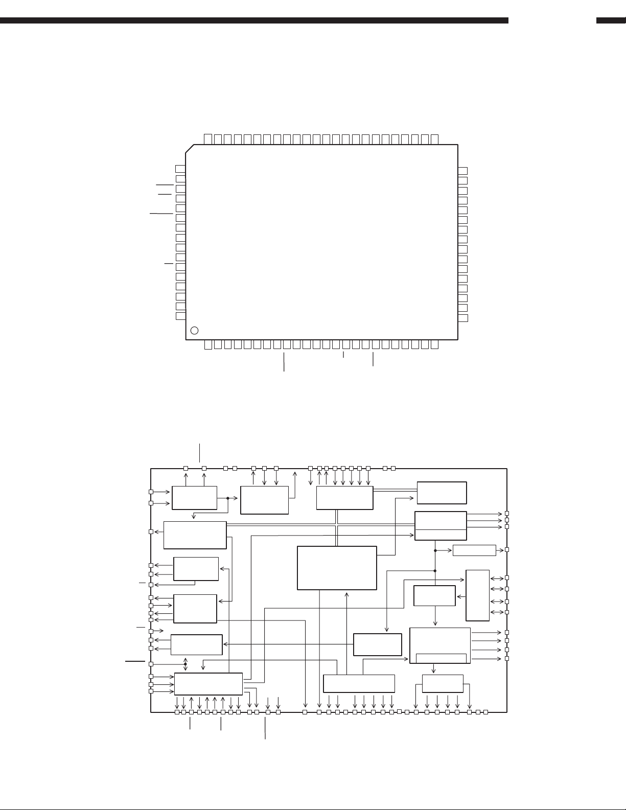
LC78625E (IC103)
DCD-1650SR
13
DCD-1650SR
)
S
2
D
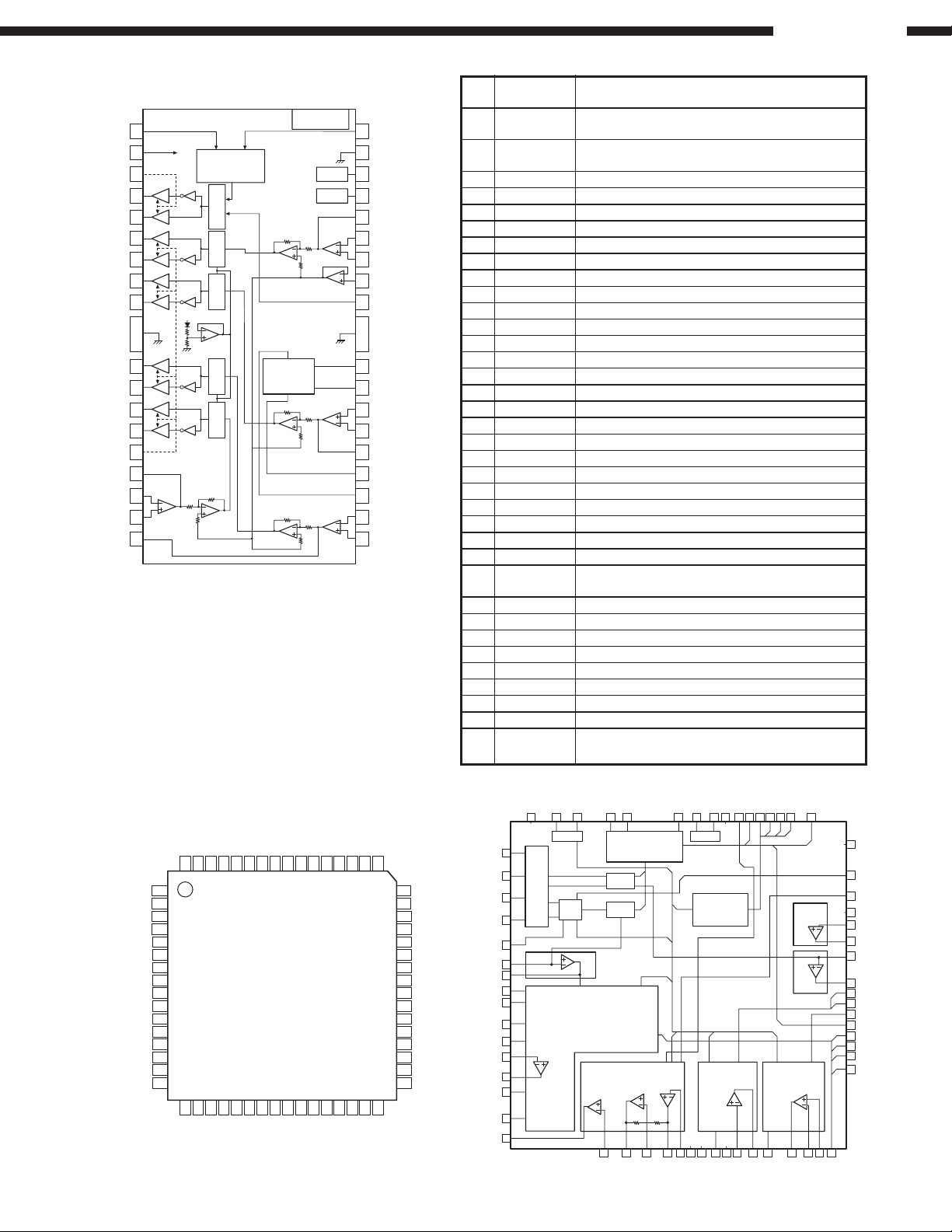
LA6559 (IC101)
1
REV
Signal System VCC
2
-VCC
VCC2
VLO-
VLO+
VO4+
VO4-
VO3+
VO3-
VO2+
VO2-
VO1+
VO1-
VCC1
VIN1
VIN1-
VIN1+
VIN2
FR
3
4
5
6
7
8
9
Power
System
GND
FR
10
11
12
13
14
15
16
17
18
Power Supply
(LOADING)
(Forward/Reverse/
Power Supply
(CH1 to CH4)
11k
Input
Break/OFF)
Control
Output
Level
Shift
Level
Shift
Level
Shift
Level
Shift
33k
Signal System GND
CH2 to CH4
Output
CH1 Output
ON/OFF
33k
Power System GND
3.3VREG
(External PNP)
33k
3.3VREG GND
3.3VREG
Power Supply
33k
Thermal
Shutdown
MUTE2
MUTE1
11k
PNP Tr
Collector
11k
11k
PNP Tr
Base
FWD
36
S-GND
35
MUTE2
34
33
MUTE1
32
VIN4
31
VIN4-
30
VIN4+
29
VREF-IN
28
VCONT(LOADING
FR
FR
27
REG-OUT
26
REG-IN
25
VIN3+
24
VIN3-
23
VIN3
22
GND-VREG
21
VCC-VREG
20
VIN2+
19
VIN2-
Pin
No.
1 REV
2 S-Vcc
Name
5CH output change terminal, logic input of
loading block
signal system power supply
(BTL-AMP:CH1~4)
Function
3 Vcc2 Power supply for loading block
4 VL0− Loading output (−)
5 VL0+ Loading output (+)
6 VO4+ Output terminal (+) for channel 4
7 VO4− Output terminal (−) for channel 4
8 VO3+ Output terminal (+) for channel 3
9 VO3− Output terminal (−) for channel 3
10 VO2+ Output terminal (+) for channel 2
11 VO2− Output terminal (−) for channel 2
12 VO1+ Output terminal (+) for channel 1
13 VO1− Output terminal (−) for channel 1
14 Vcc1 CH1~CH4(BTL-AMP) output stage power supply
15 VIN1 Input terminal for channel 1
16 VIN1− OP-AMP input AMP-A input terminal (−)
17 VIN1+ OP-AMP input AMP-A input terminal (+)
18 VIN2 Input terminal for channel 2, input AMP output
19 VIN2− Input terminal (−) for channel 2
20 VIN2+ Input terminal (+) for channel 2
21 Vcc-VREG 3.3VREG power supply
22 GND-VREG 3.3VREG GND
23 VIN3 Input terminal for channel 3, input AMP output
24 VIN3− Input terminal (−) for channel 3
25 VIN3+ Input terminal (+) for channel 3
26 REG-IN PNP transistor base connected
27 REG-OUT
3.3V power output to which the PNP transistor
collector connected
28 VCONT Loading output voltage set terminal
29 VREF-IN Reference voltage applied terminal
30 VIN4+ Input terminal (+) for channel 4
31 VIN4− Input terminal (−) for channel 4
32 VIN4 Input terminal for channel 4, input AMP output
33 MUTE1 Output ON/OFF for channel 1 (BTL AMP)
34 MUTE2 Output ON/OFF for channel 2 to 4 (BTL AMP)
35 S-GND Signal system GND
36 FWD
Output change terminal (FWD) for loading
output (VLO+−), logic input of loading block
LA9241M (IC102)
VCC1
LDS
LDD
BH1
APC
I/V
T. SERVO & T.LOGIC
FIN2
FIN1
TE
TESI
SCI
TD
TO
FD
TB
TE
TH
TA
TD
JP
VCC1
LDS
LDD
BH1
PH1
LF2
VR
646362616059585756555453525150
1
2
E
3
F
4
5
6
7
8
9
10
11
12
13
14
15
16
171819202122232425262728293031
-
FD
-
FAFAFE
NC
FE
GND
REFI
SP
VCC
SPG
FSS
DRFCEDATCLCLK
-
SP
SPD
SLEQ
SLD
DEF
49
48
NC
47
TBC
46
FSC
45
DGND
44
SLI
43
SLC
32
-
-
+
JP
SL
SL
-
42
RFS
41
RFSM
+
40
CV
-
39
CV
38
SLOF
37
HFL
36
TES
35
TOFF
34
TGL
+
33
JP
FIN2
FIN1
TESI
1
2
3
E
4
F
5
TB
6
TE
TE
7
8
9
SCI
10
TH
TA
11
-
TD
12
TD
13
JP
14
TO
15
FD
16
PH1
RF DET
VCA
VCABAL
TE
F.SERVO & F.LOGIC
17 18 19 20 21 22 23 24 25 26 27 28 29 30 31 32
FA
FD
FAFEFE
LF2VRREFI
REF
INTER FACE
NC
AGND
VCC2FSS
m
-com
SPINDLE
SERVO
SP
SPG
DRFCEDATCLCLK
SP
SPD
SLC
RF Amp
SLED SERVO
SLD
SLEQ
DEF
49505152535455565758596061626364
-
+
SLSLJP
NC
48
47
TBC
FSC
46
45
DGN
SLI
44
SLC
43
-
42
RFS
RFSM
41
+
CV
40
-
CV
39
SLOF
38
37
HFL
TES
36
TOFF
35
TGL
34
+
33
JP
-
14
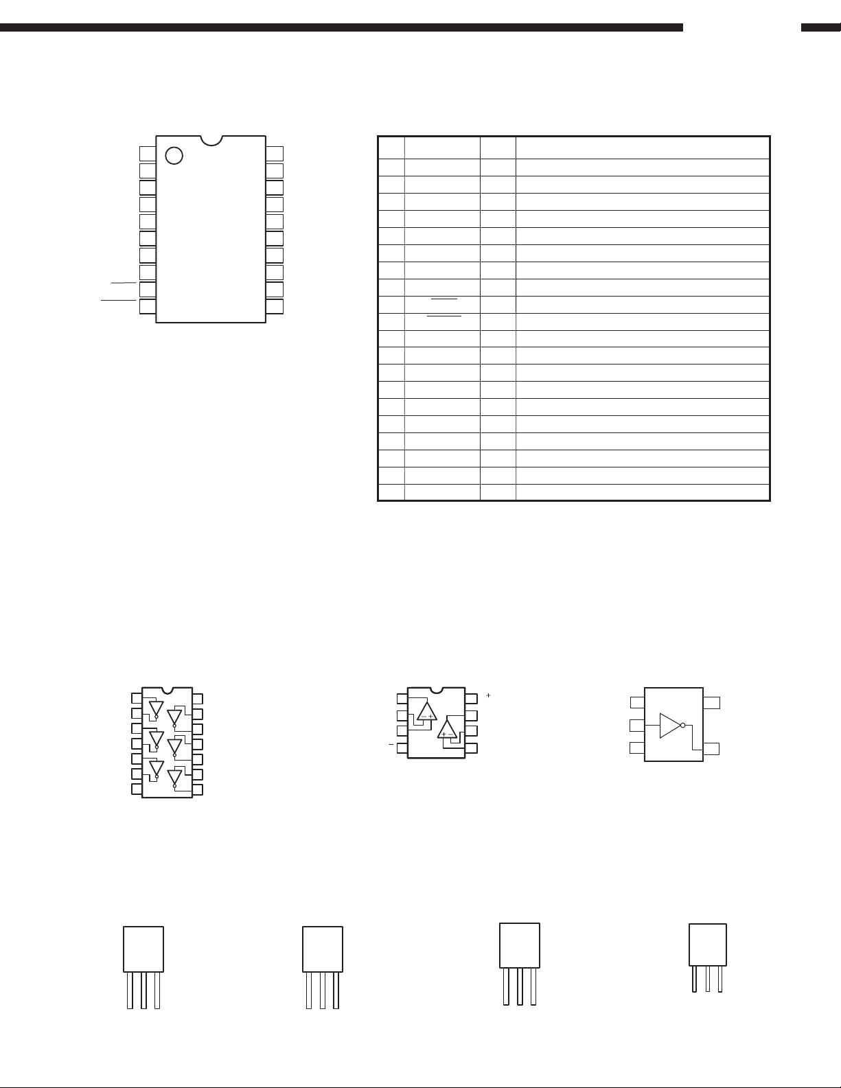
PCM1704U (IC601~604)
PCM1704U (IC601~604)
DATA
1
BCLK
2
NC
3
V
4
−
DD
DGND
5
+V
6
DD
WCLK
7
NC
8
9
20BIT
INVERT
10
20
−V
19
REF DC
18
NC
17
SERVO DC
16
AGND
15
AGND
14
I
OUT
13
NC
12
BPO DC
11
+V
DCD-1650SR
Pin
Symbol Function
CC
CC
No.
1
2
3
4
5
6
7
8
9
10
11
12
13
14
15
16
17
18
19
20
DATA
BCLK
NC
-V
DD
DGND
+V
DD
WCLK
NC
20BIT
INVERT
+V
CC
BPO DC
NC
I
OUT
AGND
AGND
SERVO DC
NC
REF DC
-V
CC
Remarks:
(1) Not connected (Not used)
(2) Internal Pull -up
I/O
IN
Serial Audio Input
IN
Bit Clock Input for Serial Audio Data Input
NC (1)
Digital Power Supply -5V
Digital GND
Digital Power Supply +5V
Data Latch Accept Input
NC (1)
INPUT Data Language Select (2)
IN
INPUT Data Polarity Select (2)
IN
Analog Power Supply +5V
Bipotar Offset De-Coupling Capacitor
NC (1)
Audio Signal Analog Current Output
OUT
Analog GND
Analog GND
Servo Amp De-coupling Capacitor
NC (1)
Band Cap. Reference De-coupling Capacitor
Analog Power Supply -5V
TC74HCU04AF (IC202)
GND
1
1A
2
1Y
3
2A
4
2Y
5
3A
6
3Y
7
Vcc
14
13
6A
6Y
12
11
5A
10
5Y
9
4A
8
4Y
NJM7805FA (IC804)
NJM7806FA (IC803)
NJM7812FA (IC801)
FRONT
VIEW
NJM4556AD (IC501, 502)
OP275GP (IC607~612)
BA15218 (IC104)
OPA2134PA (IC613, 614)
A OUTPUT
A I NPUT
A+INPUT
1
2
3
V
4
NJM7905FA (IC353, 354)
NJM79M12FA (IC802)
FRONT
VIEW
V
2
8
B OUTPUT
7
6
B I NPUT
B +INPUT
5
1
NJM78L05A (IC351, 352)
FRONT
VIEW
TC7SU04F (IC203)
NC
1
IN A
2
GND
3
PST600C (IC401)
FRONT
5
4
VIEW
Vcc
OUT Y
Input
GND
Output
GND
Input
Output
Output
GND
Input
DD
V
Out
GND
15
 Loading...