

Page 1
e
SERVICE MANUAL
MODEL JP E3 E2 EK EA E1 E1K E1C
Ver. 1
AVR-X3000
INTEGRATED NETWORK AV RECEIVER
P P P
• For purposes of improvement, specications and design are subject to change without notice.
Please use this service manual with referring to the operating instructions without fail.
•
Some illustrations using in this service manual are slightly different from the actual set.
•
e
D&M Holdings Inc.
S0636-0V01DM/DG1304
Copyright 2013 D&M Holdings Inc. All rights reserved.
WARNING: Violators will be prosecuted to the maximum extent possible.
Page 2

CONTENTS
ABOUT THIS MANUAL
What you can do with this manual ............................................3
Using Adobe Reader (Windows version) ..................................4
SAFETY PRECAUTIONS
NOTE FOR SCHEMATIC DIAGRAM
NOTE FOR PARTS LIST
TECHNICAL SPECIFICATIONS
DIMENSION
CAUTION IN SERVICING
Initializing INTEGRATED NETWORK AV RECEIVER ............10
Service Jig ..............................................................................10
DISASSEMBLY
1. FRONT PANEL ASSY ........................................................13
2. HEAT SINK ASSY ..............................................................14
3. DIGITAL UNIT ASSY ..........................................................15
4. TRANS MAIN .....................................................................17
SPECIAL MODE
1. µcom/DSP Version display mode .......................................19
2. PANEL/REMOTE LOCK Selection mode ...........................23
3. Service Related Selection mode ........................................24
4. Protection Pass mode ........................................................56
5. DM860A Reboot mode .......................................................56
6. Remote ID Setup mode ......................................................57
JIG FOR SERVICING
WHEN THE MICROPROCESSOR IS
REPLACED WITH A NEW ONE
PROCEDURE FOR UPGRADING
THE VERSION OF THE FIRMWARE
1. How to update by DFW ......................................................61
2. How to update by DPMS ....................................................65
3. How to update by USB Memory .........................................72
ADJUSTMENT
Sound modes and channel output
TROUBLE SHOOTING
1. POWER ..............................................................................85
2. Analog video ......................................................................86
3. HDMI/DVI ...........................................................................89
4. AUDIO ................................................................................91
5. Network/USB ......................................................................94
6. SMPS .................................................................................97
Audio Check PASS
CLOCK FLOW & WAVE FORM IN DIGITAL BLOCK
LEVEL DIAGRAM
POWER DIAGRAM
WIRING DIAGRAM
PRINTED WIRING BOARDS
...............................................................................9
.........................................................................81
.............................................................3
..........................................................6
.........................................7
...........................................................7
................................................9
........................................................10
........................................................................11
......................................................................18
..............................................................58
..............................................61
......................................61
........................................82
............................................................85
................................................................99
...........100
..................................................................101
................................................................107
................................................................108
.................................................109
SCHEMATIC DIAGRAMS (1/30)
SCH01_DIG_CONNECT.......................................................11 8
SCH02_DIG_POWER ...........................................................11 9
SCH03_DIG_MAIN_CPU ......................................................120
SCH04_DIG_SUB_CPU .......................................................121
SCH05_DIG_CPU_LEVEL_CHG .........................................122
SCH06_DIG_DIR ..................................................................123
SCH07_DIG_AUDIO_PLD ....................................................124
SCH08_DIG_DSP1 ...............................................................125
SCH9_DIG_MAIN_DAC1 ......................................................126
SCH10_DIG_DM860 .............................................................127
SCH11_DIG_ETHERNET_PHY ............................................128
SCH12_DIG_HDMI_RX ........................................................129
SCH13_DIG_SII9575 ............................................................130
SCH14_DIG_FRONT_HDMI .................................................131
SCH15_DIG_HDMI TX..........................................................132
SCH16_FRONT ....................................................................133
SCH17_INPUT ......................................................................134
SCH18_INPUT ......................................................................135
SCH19_INPUT_PREOUT .....................................................136
SCH20_INPUT_F-HDMI .......................................................137
SCH21_VIDEO .....................................................................138
SCH22_VIDEO_RC5_MXPORT ...........................................139
SCH23_VIDEO_RS232C_TRIGGER ...................................140
SCH24_AMP_AMP1 .............................................................141
SCH25_AMP_AMP2 .............................................................142
SCH26_SPK .........................................................................143
SCH27_SPK_REGULATOR_TUNER ...................................144
SCH28_CNT_CONNECT_A .................................................145
SCH29_CNT_CONNECT_B .................................................146
SCH30_SMPS ......................................................................147
EXPLODED VIEW
PACKING VIEW
SEMICONDUCTORS
1. IC's ...................................................................................151
2. FL DISPLAY .....................................................................179
.................................................................148
.....................................................................149
.............................................................151
...........................................11 8
2
Page 3
ABOUT THIS MANUAL
Read the following information before using the service manual.
What you can do with this manual
Search for a Ref. No. (phrase)
(Ctrl+Shift+F)
You can use the search function in Acrobat Reader to
search for a Ref. No. in schematic diagrams, printed
wiring board diagrams, block diagrams, and parts
lists.
1.Press
• The Search window appears.
2.Enter the Ref. No. you want to search for in the
Search window, and then click the
•A list of search results appears.
Ctrl+Shift+F
Shift
Ctrl
on the keyboard.
F
Search
button.
Jump to the target of a schematic
diagram connector
Click the Ref. No. of the target connector in the red
box around a schematic diagram connector.
•The screen jumps to the target connector.
3.Click an item on the list.
• The screen jumps to the page for that item, and the
search phrase is displayed.
• Page magnication stays the same as before the
jump.
3
Page 4
Using Adobe Reader (Windows version)
Add notes to this data (Sign)
The Sign function lets you add notes to the data in
this manual.
Save the le once you have nished adding notes.
[Example using Adobe Reader X]
"View"
On the
• The Sign pane appears.
[Example using Adobe Reader 9]
On the
menu, click
"Document"
"Sign"
menu, click
.
"Sign"
.
Magnify schematic / printed wiring
board diagrams - 1
(Ctrl+Space, mouse operation)
Ctrl+Space
Press
mouse to select the area you want to view.
• The selected area is magnied.
• When you want to move the area shown, hold
Space
down
• When you want to show a full page view, press
Ctrl+0
on the keyboard.
on the keyboard and drag the
0
Ctrl Space
and drag the mouse.
Print a magnied part of the manual
The Properties dialog box and functions will vary depending on your printer.
1. Drag the mouse to magnify the part you want to print.
2. On the
3. Congure the following settings in the Print dialog box.
"File"
menu, click
"Print"
.
• Properties
Click this button and check that the printer is set to a
suitable paper size.
• Page to print
Select the following checkbox.
More Options
"
• Page Sizing & Handling
Select the following checkbox.
Size
"
Size Options
" / "
Current View
" : "
" : "
Fit
"
"
4. Click the
Print
button to start printing.
4
Page 5
Magnify schematic / printed wiring
board diagrams - 2
(Pan & Zoom function)
The Pan & Zoom function lets you see which part of
a magnied diagram is being shown in a separate
window.
[Example using Adobe Reader X]
"View"
On the
"Pan & Zoom"
menu, point to
.
"Zoom"
, and then click
Magnify schematic / printed wiring
board diagrams - 3
(Loupe Tool function)
The Loupe Tool function lets you magnify a specic
part of a diagram in a separate window.
[Example using Adobe Reader X]
On the
"Loupe Tool"
"View"
menu, point to
.
"Zoom"
, and then click
• The Pan & Zoom window appears on the screen.
[Example using Adobe Reader 9]
"Tools"
On the
then click
menu, point to
"Pan & Zoom Window"
"Select & Zoom"
.
, and
• The Loupe Tool window appears on the screen.
[Example using Adobe Reader 9]
"Tools"
On the
then click
menu, point to
"Loupe Tool Window"
"Select & Zoom"
.
, and
5
Page 6

SAFETY PRECAUTIONS
The following items should be checked for continued protection of the customer and the service technician.
leakage current check
Before returning the set to the customer, be sure to carry out either (1) a leakage current check or (2) a line to chassis
resistance check. If the leakage current exceeds 0.5 milliamps, or if the resistance from chassis to either side of the
power cord is less than 460 kohms, the set is defective.
Be sure to test for leakage current with the AC plug in both polarities, in addition, when the set's power is in each state
(on, off and standby mode), if applicable.
CAUTION
Please heed the following cautions and instructions during servicing and
inspection.
◎Heed the cautions!
Cautions which are delicate in particular for servicing
are labeled on the cabinets, the parts and the chassis,
etc. Be sure to heed these cautions and the cautions
described in the handling instructions.
◎Cautions concerning electric shock!
(1) An AC voltage is impressed on this set, so if you
touch internal metal parts when the set is energized,
you may get an electric shock. Avoid getting an
electric shock, by using an isolating transformer
and wearing gloves when servicing while the set is
energized, or by unplugging the power cord when
replacing parts, for example.
(2) There are high voltage parts inside. Handle with
extra care when the set is energized.
◎ Caution concerning disassembly and
assembly!
Through great care is taken when parts were
manufactured from sheet metal, there may be burrs on
the edges of parts. The burrs could cause injury if ngers
are moved across them in some rare cases. Wear gloves
to protect your hands.
◎Use only designated parts!
The set's parts have specic safety properties (re
resistance, voltage resistance, etc.). Be sure to use parts
which have the same properties for replacement. The
burrs have the same properties. In particular, for the
important safety parts that are indicated by the z mark
on schematic diagrams and parts lists, be sure to use
the designated parts.
◎ Be sure to mount parts and arrange the wires
as they were originally placed!
For safety seasons, some parts use tapes, tubes or other
insulating materials, and some parts are mounted away
from the surface of printed circuit boards. Care is also
taken with the positions of the wires by arranging them
and using clamps to keep them away from heating and
high voltage parts, so be sure to set everything back as
it was originally placed.
◎Make a safety check after servicing!
Check that all screws, parts and wires removed or
disconnected when servicing have been put back in their
original positions, check that no serviced parts have
deteriorate the area around. Then make an insulation
check on the external metal connectors and between
the blades of the power plug, and otherwise check that
safety is ensured.
(Insulation check procedure)
Unplug the power cord from the power outlet, disconnect
the antenna, plugs, etc., and on the power. Using a 500V
insulation resistance tester, check that the insulation
resistance value between the inplug and the externally
exposed metal parts (antenna terminal, headphones
terminal, input terminal, etc.) is 1MΩ or greater. If it is
less, the set must be inspected and repaired.
CAUTION
Concerning important
safety parts
Many of the electric and the structural parts used in the
set have special safety properties. In most cases these
properties are difcult to distinguish by sight, and the use
of replacement parts with higher ratings (rated power
and withstand voltage) does not necessarily guarantee
that safety performance will be preserved. Parts with
safety properties are indicated as shown below on the
wiring diagrams and the parts list in this service manual.
Be sure to replace them with the parts which have the
designated part number.
(1) Schematic diagrams .......Indicated by the z mark.
(2) Parts lists .......Indicated by the z mark.
The use of parts other than the
designated parts could cause electric
shocks, res or other dangerous
situations.
6
Page 7
NOTE FOR SCHEMATIC DIAGRAM
NOTE FOR PARTS LIST
WARNING:
Parts indicated by the z mark have critical characteristics. Use ONLY replacement parts recommended by the manufacturer.
CAUTION:
Before returning the set to the customer, be sure to carry out either (1) a leakage current check or (2) a line to chassis resistance check. If
the leakage current exceeds 0.5 milliamps, or if the resistance from chassis to either side of the power cord is less than 460 kohms, the set
is defective.
WARNING:
DO NOT return the set to the customer unless the problem is identied and remedied.
NOTICE:
ALL RESISTANCE VALUES IN OHM. k=1,000 OHM / M=1,000,000 OHM
ALL CAPACITANCE VALUES ARE EXPRESSED IN MICRO FARAD, UNLESS OTHERWISE INDICATED. P INDICATES MICRO-MICRO
FARAD. EACH VOLTAGE AND CURRENT ARE MEASURED AT NO SIGNAL INPUT CONDITION. CIRCUIT AND PARTS ARE SUBJECT
TO CHANGE WITHOUT PRIOR NOTICE.
NOTE FOR PARTS LIST
1.
Parts indicated by "nsp" on this table cannot be supplied.
2.
When ordering a part, make a clear distinction between "1" and "I" (i) to avoid mis-supplying.
3.
A part ordered without specifying its part number can not be supplied.
4.
Part indicated by "★" mark is not illustrated in the exploded view.
5.
General-purpose Carbon Film Resistor in the P.W.Board parts list. (Refer to the Schematic Diagram for those parts.)
6.
General-purpose Carbon Chip Resistors are not included are not included in the P.W.Board parts list.
(Refer to the Schematic Diagram for those parts.)
WARNING:
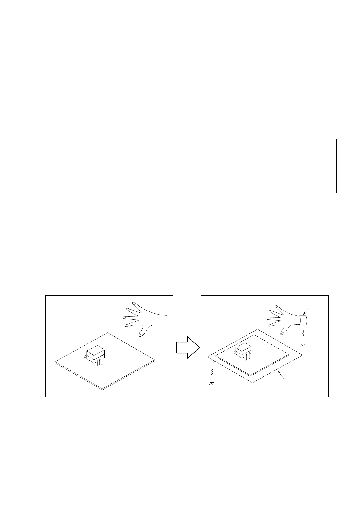
INSTRUCTIONS FOR HANDLING SEMI-CONDUCTORS AND OPTICAL UNIT
Electrostatic breakdown of the semi-conductors or optical pickup may occur due to a potential difference caused by
electrostatic charge during unpacking or repair work.
Parts indicated by the z mark have critical characteristics. Use ONLY replacement parts recommended by the manufacturer.
1. Ground for Human Body
Be sure to wear a grounding band (1 MΩ) that is properly grounded to remove any static electricity that may be
charged on the body.
2. Ground for Workbench
Be sure to place a conductive sheet or copper plate with proper grounding (1 MΩ) on the workbench or other surface,
where the semi-conductors are to be placed. Because the static electricity charge on clothing will not escape through
the body grounding band, be careful to avoid contacting semi-conductors with your clothing
<Incorrect>
<Correct>
CBA
CBA
1MΩ
Grounding Band
1MΩ
Conductive Sheet or
Copper Plate
7
Page 8

Personal notes:
8
Page 9
TECHNICAL SPECIFICATIONS
nAudio section
• Power amplifier
Rated output:
Front:
105 W + 105 W (8 Ω/ohms, 20 Hz – 20 kHz with 0.08 % T.H.D.
135 W + 135 W (6 Ω/ohms, 1 kHz with 0.7 % T.H.D.)
Center:
105 W (8 Ω/ohms, 20 Hz – 20 kHz with 0.08 % T.H.D.)
135 W (6 Ω/ohms, 1 kHz with 0.7 % T.H.D.)
Surround:
105 W + 105 W (8 Ω/ohms, 20 Hz – 20 kHz with 0.08 % T.H.D.)
135 W + 135 W (6 Ω/ohms, 1 kHz with 0.7 % T.H.D.)
Surround back:
105 W + 105 W (8 Ω/ohms, 20 Hz – 20 kHz with 0.08 % T.H.D.)
135 W + 135 W (6 Ω/ohms, 1 kHz with 0.7 % T.H.D.)
Output connectors:
• Analog
Input sensitivity/Input impedance:
Frequency response:
S/N :
100 dB (IHF–A weighted, DIRECT mode)
6 – 16 Ω/ohms
200 mV/47 kΩ/kohms
10 Hz – 100 kHz — +1, –3 dB (DIRECT mode)
nTuner section
(Note: μV at 75 Ω/ohms, 0 dBf = 1 x 10
Receiving Range:
Usable Sensitivity:
50 dB Quieting
Sensitivity:
S/N :
Total harmonic
Distortion:
FM 87.5 MHz – 107.9 MHz
AM 530 kHz – 1710 kHz
FM 1.2 μV (12.8 dBf)
AM 18 μV
MONO 2.8 μV (20.2 dBf)
MONO 70 dB (IHF–A weighted, DIRECT mode)
STEREO 67 dB (IHF–A weighted, DIRECT mode)
MONO 0.7 % (1 kHz)
STEREO 1.0 % (1 kHz)
nGeneral
Power supply:
Power consumption:
Power consumption in standby mode:
Power consumption in CEC standby mode:
Power consumption in network standby mode:
AC 120 V, 60 Hz
AC 230 V, 50/60 Hz
600 W
0.1 W
–15
W)
0.5 W
2.7 W
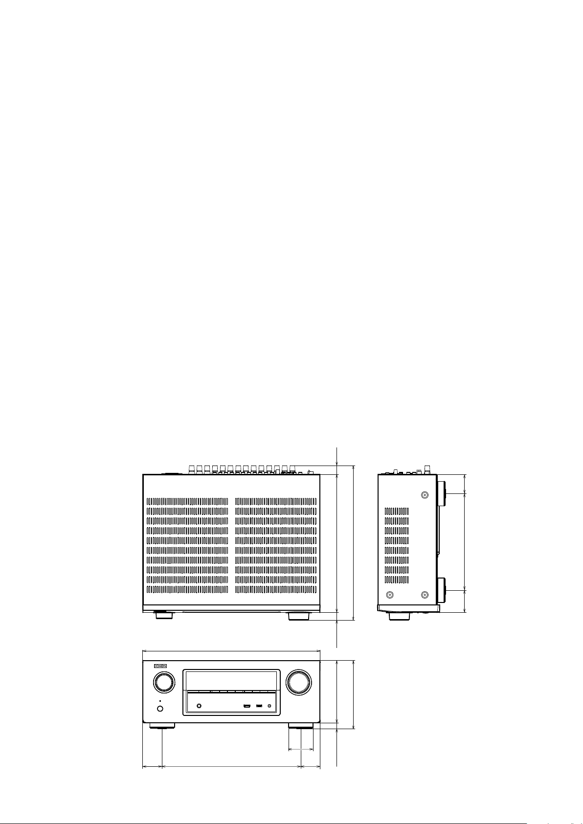
DIMENSION
Unit : in. (mm)
Weight : 23 lbs 9 oz (10.7 kg
17 3/32 (434.0)
55/64
(22.0)
13 21/64 (338.5)
14 59/64 (379.0)
47/64
(18.5)
(47.0)
1 27/32
9 21/64 (236.8)
(54.7)
2 5/32
1 27/32
(47.0)
13 25/64 (340.0)
2 23/64
(60.0)
1 27/32
(47.0)
6 37/64 (167.0)
19/32 (15.0) 5 63/64 (152.0)
9
Page 10
CAUTION IN SERVICING
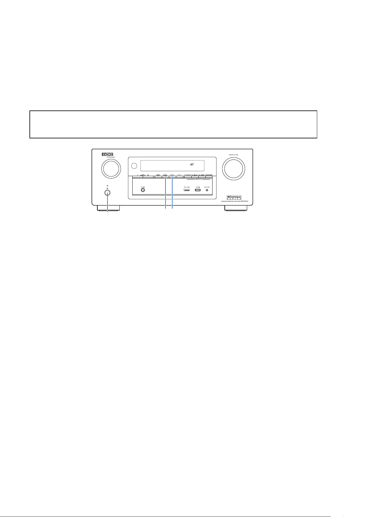
Initializing INTEGRATED NETWORK AV RECEIVER
INTEGRATED NETWORK AV RECEIVER initialization should be performed when the μcom, peripheral parts of μcom, and
Digital P.W.B. were replaced.
1. Turn off the power pressing "X"button.
2. Press "X" button while simultaneously while pressing
3. Check that the entire display is ashing at intervals of about 1 second, and then release the 2 buttons.
The microprocessor will be initialized.
NOTE: • If step 3 fails, start over from step 1.
• All user settings will be lost and the factory setting will be recovered after the set is initialized.
So make sure to note down your setting beforehand for restoring after the initialization.
"ZONE2 SOURCE"
and
"DIMMER"
buttons.
X
ZONE2 SOURCE DIMMER
Service Jig
When you repair the printing board, you can use the following JIG (Extension cable kit).
Please order it from Denon Ofcial Service Distributor in your region if necessary.
8U-110084S : EXTENSION UNIT KIT : 1 Set
(Refer to 58 page.)
10
Page 11
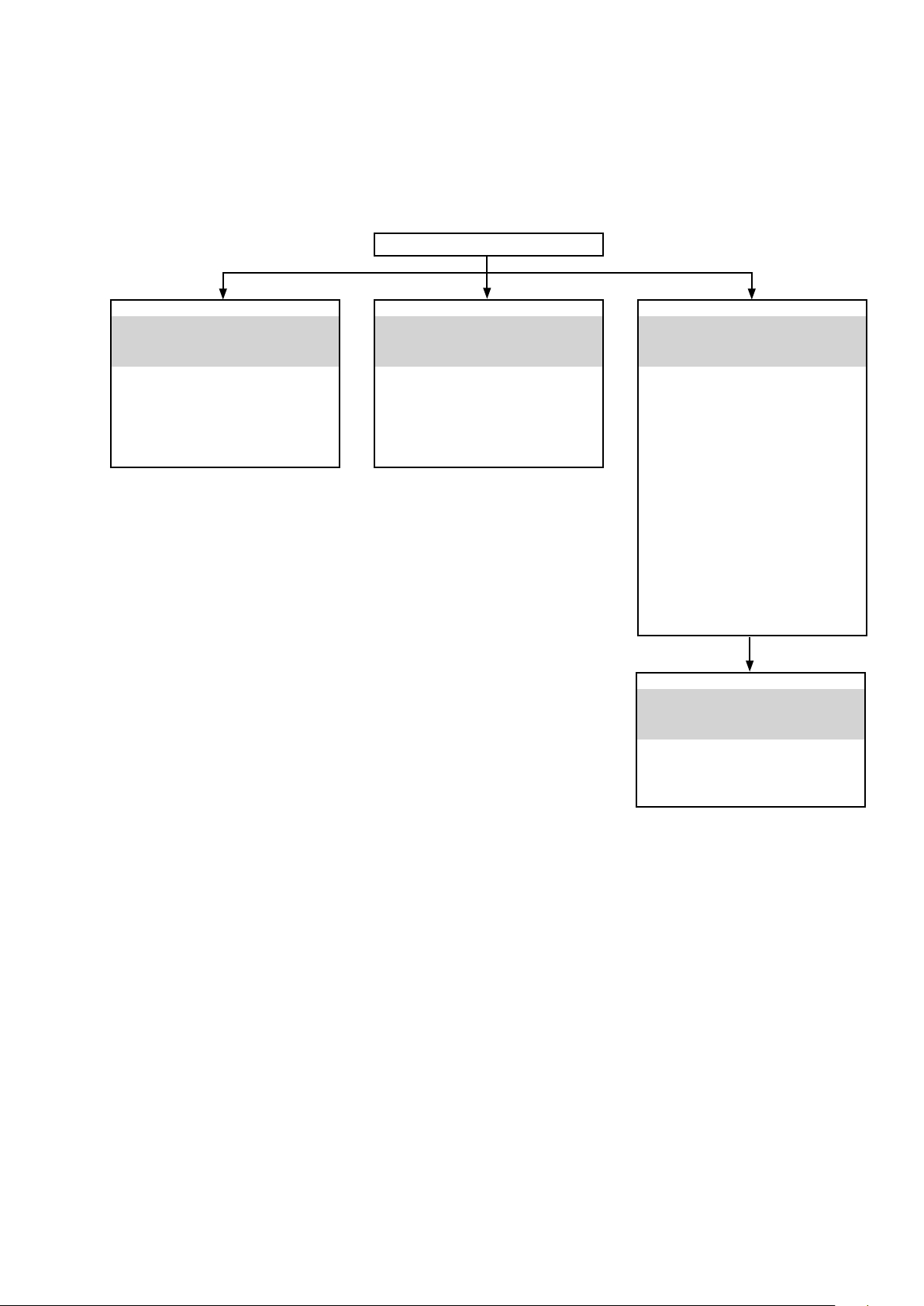
DISASSEMBLY
• Disassemble in order of the arrow in the following gure.
• In the case of the re-assembling, assemble it in order of the reverse of the following ow.
• In the case of the re-assembling, observe "attention of assembling".
• If wire bundles are untied or moved to perform adjustment or replace parts etc., be sure to rearrange them neatly as
they were originally bundled or placed afterward.
Otherwise, incorrect arrangement can be a cause of noise generation.
CABINET TOP
FRONT PANEL ASSY
"DISASSEMBLY
Refer to
1. FRONT PANEL ASSY"
"EXPLODED VIEW"
and
PCB FRONT
(Ref. No. of EXPLODED VIEW : C1)
PCB FRONT HDMI FFC CABLE
(Ref. No. of EXPLODED VIEW : C2)
PCB FRONT HDMI
(Ref. No. of EXPLODED VIEW : C3)
HEAT SINK ASSY
"DISASSEMBLY
Refer to
2. HEAT SINK ASSY"
"EXPLODED VIEW"
and
PCB GUIDE L
(Ref. No. of EXPLODED VIEW : C5)
7CH AMP PCB ASSY
(Ref. No. of EXPLODED VIEW : C6)
PCB GUIDE FFC
(Ref. No. of EXPLODED VIEW : C7)
DIGITAL UNIT ASSY
"DISASSEMBLY
Refer to
3. DIGITAL UNIT ASSY"
"EXPLODED VIEW"
and
PCB SMPS
(Ref. No. of EXPLODED VIEW : C4)
PCB FRONT_CNT
(Ref. No. of EXPLODED VIEW : C10)
PCB FUSE
(Ref. No. of EXPLODED VIEW : C11)
PCB SPK_PREOUT
(Ref. No. of EXPLODED VIEW : C12)
PCB SIDE_CNT
(Ref. No. of EXPLODED VIEW : C13)
PCB INPUT
(Ref. No. of EXPLODED VIEW : C14)
PCB VIDEO
(Ref. No. of EXPLODED VIEW : C15)
PCB DIGITAL
(Ref. No. of EXPLODED VIEW : C16)
POWER TRANS
"DISASSEMBLY
Refer to
4. POWER TRANS"
"EXPLODED VIEW"
and
PCB TRANS TEMP
(Ref. No. of EXPLODED VIEW : C8)
TRANS , POWER
(Ref. No. of EXPLODED VIEW : C9)
11
Page 12
About the photos used for "descriptions of the DISASSEMBLY" section
• The shooting direction of each photograph used herein is indicated on the left side of the respective photograph as
"Shooting direction: ***".
• Refer to the diagram below about the shooting direction of each photograph.
• Photographs with no shooting direction indicated were taken from the top of the set.
The viewpoint of each photograph
(Shooting direction X)
[View from the top]
Shooting direction: C
Shooting direction: B
Front side
Shooting direction: D
Shooting direction: A
12
Page 13
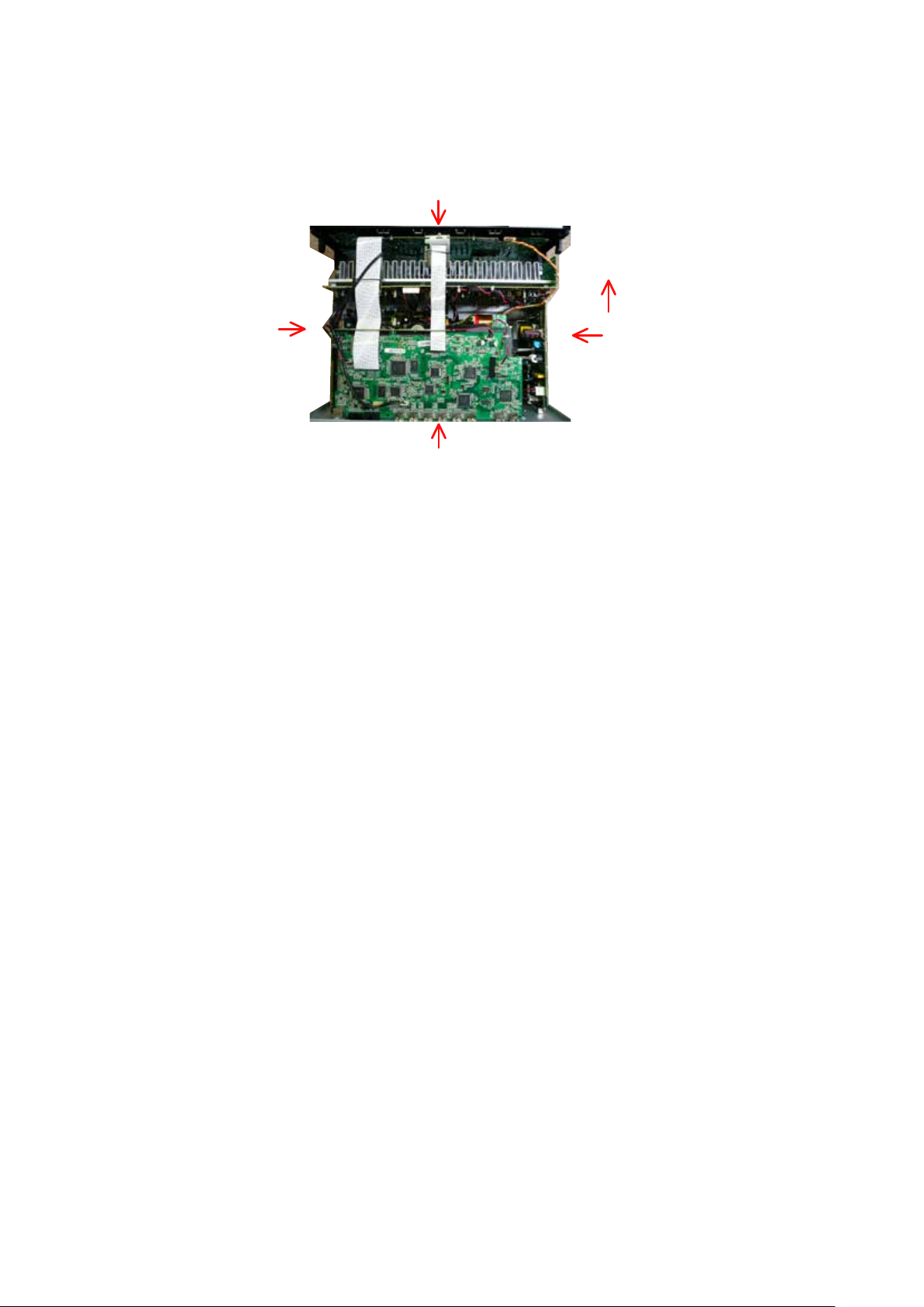
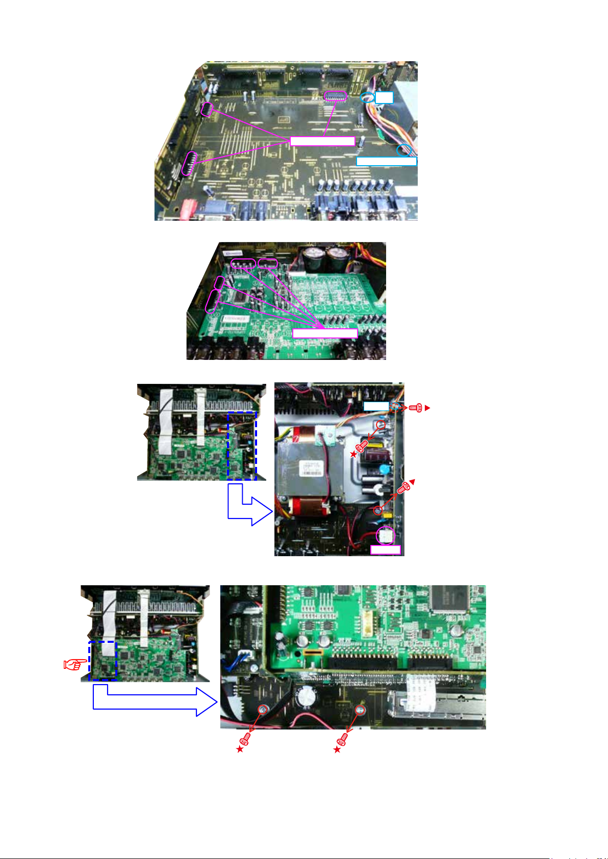
1. FRONT PANEL ASSY
Proceeding : CABINET TOP→FRONT PANEL ASSY
(1) Remove the screws.
View from the bottom
(2) Disconnect the connector wires and FFC. Remove the Style pin and screws.
STYLE PIN : Loosen
CN602
cut
FFC cable
CN321
13
Page 14
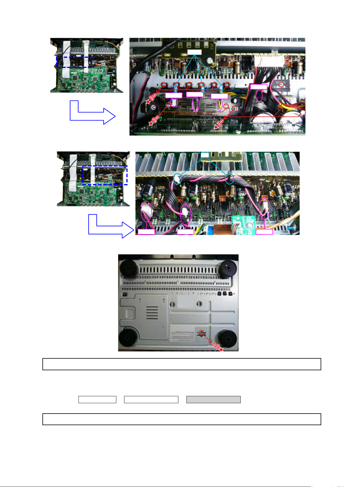
2. HEAT SINK ASSY
Proceeding : CABINET TOP
(1) Remove the screws.
HEAT SINK ASSY
→
View from the bottom
(2) Cut the wire clamp band, then remove the screws. Disconnect the connector wires.
Shooting direction: C
cut
(3) Cut the wire clamp band, then disconnect the connector wire and FFC cables .
STYLE PIN : Loosen
STYLE PIN : Loosen
CN602
Shooting direction: D
CN602
CN461
cut
CN704
FFC cable
CN321
(4) Cut the wire clamp bands, then disconnect the connector wires.
CN701 CN703 CN702
cut
cut
Please refer to "EXPLODED VIEW" for the disassembly method of each P.W.B included in HEAT SINK ASSY.
14
Page 15
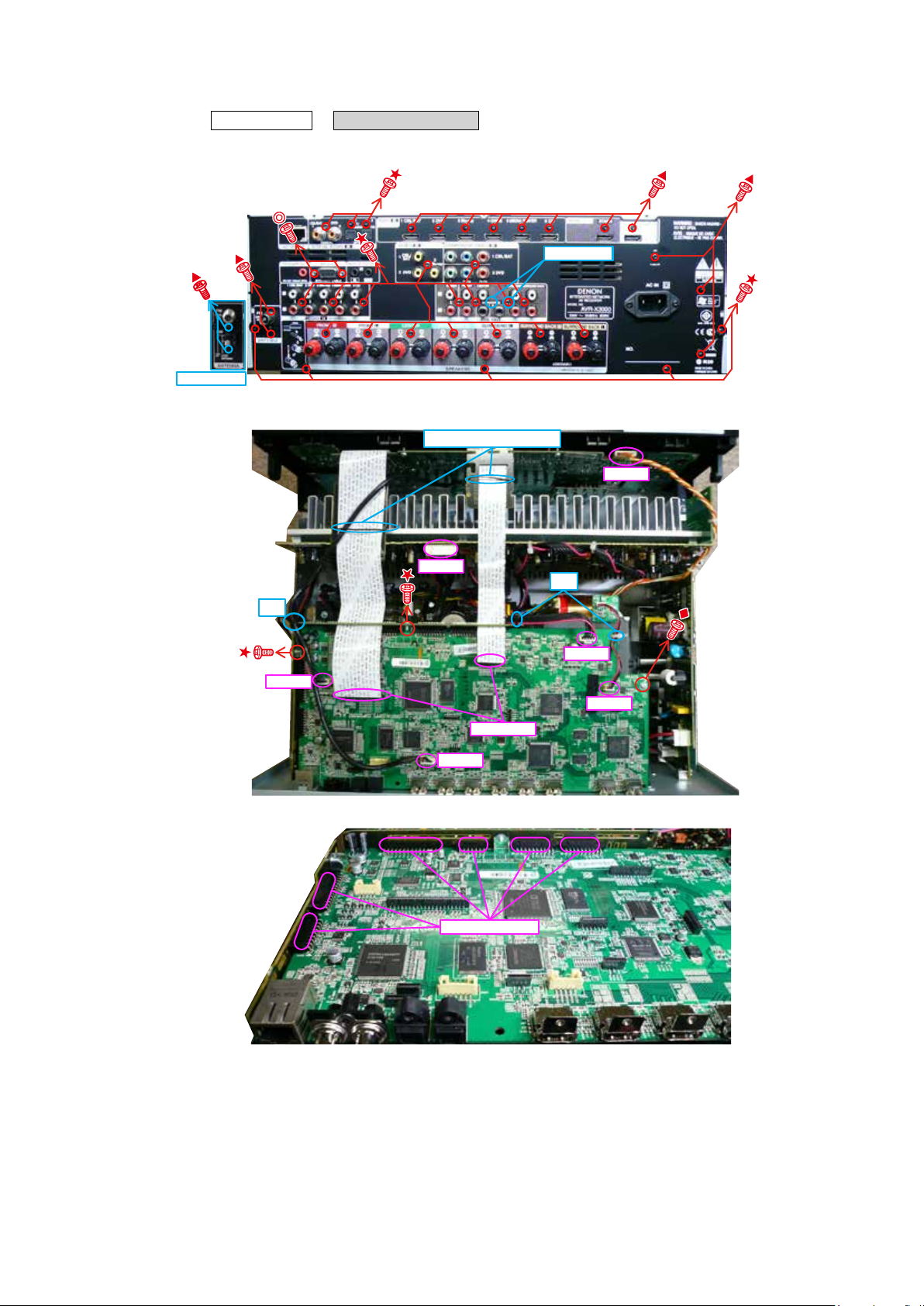
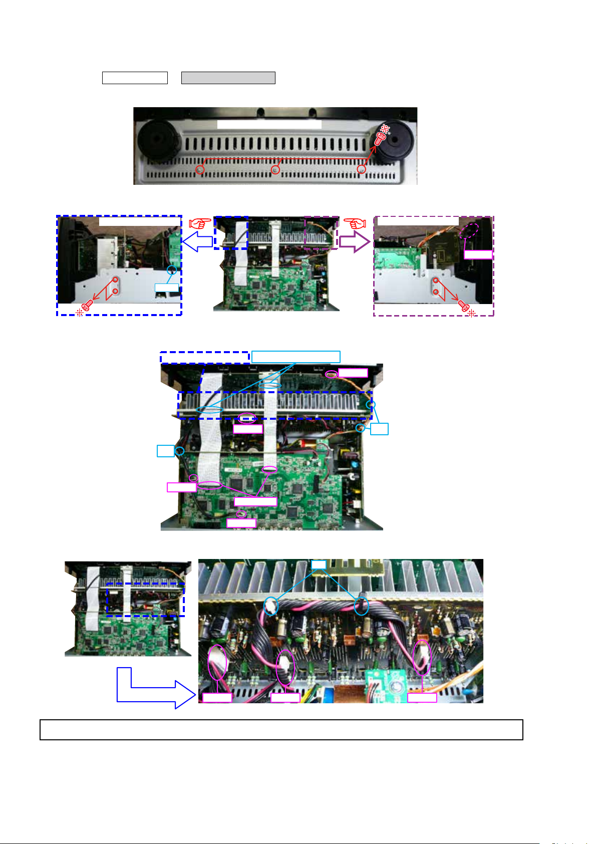
3. DIGITAL UNIT ASSY
Proceeding : CABINET TOP
(1) Remove the screws, then remove the BACK PANEL and the DIGITAL BRACKET.
E3 ONLY
(2) Cut the wire clamp band, then remove the screws. Disconnect the connector wires and FFC cables.
cut
DIGITAL UNIT ASSY
→
Shooting of photograph: A
E3 ONLY
STYLE PIN : Loosen
CN602
CN461
cut
CN704
(3) Disconnect the connector board.
CN903
CN203
FFC cable
CN321
Board to board
15
Page 16
(4) Disconnect the connector board.
(5) Disconnect the connector board
cut
Board to board
SUPPORT PCB
Board to board
(6) Cut the wire clamp band, then remove the screws. Disconnect the connector wires and FFC cables.
cut
CN932
(7) Disconnect the connector wire.
16
Shooting direction: C
Page 17
(8) Cut the wire clamp band, then remove the screws. Disconnect the connector wires.
cut
CN941
(9) Cut the wire clamp band, then disconnect the connector wires.
CN932
CN940
cut
CN971
CN701 CN703 CN702
(10) Remove the screw.
View from the bottom
Please refer to "EXPLODED VIEW" for the disassembly method of each P.W.B included in DIGITAL UNIT ASSY.
4. TRANS MAIN
Proceeding : CABINET TOP
Please refer to "EXPLODED VIEW" for the disassembly method of each P.W.B included in TRANS MAIN.
DIGITAL UNIT ASSY
→
POWER TRANS
→
17
Page 18
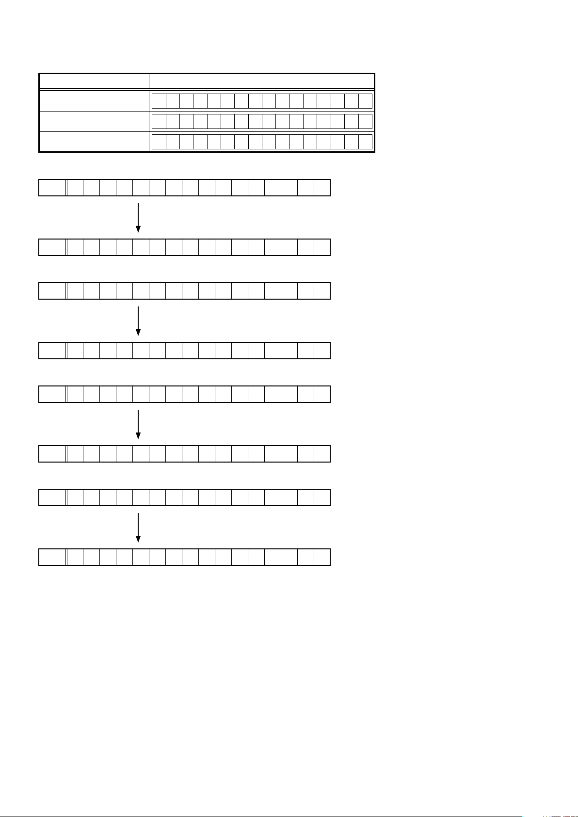
SPECIAL MODE
Special mode setting button
No.1 - 5, 7, 8 : Press the
b
No.6 : Turn on the power, then press and hold down the A and B buttons for over 3 seconds.
b
No. Mode Button A Button B Button C Contents
Version display
1
(μcom/DSP Error Display)
User Initialization mode
2
(Installer Setup settings are not
initialized.)
Factory Initialization mode
3
(Installer Setup settings are also
initialized.)
PANEL/REMOTE LOCK Selection
4
mode
5 Service Related Selection mode
6 Remote ID Setup mode STATUS DIMMER -
Mode for switching tuner frequency
7
step
(E2 model Only)
8 Installer Setup mode
same time.
"Power operation (X)"
STATUS DIMMER -
TUNER
PRESET CH
+
ZONE2
SOURCE
ZONE2
SOURCE
ZONE2
SOURCE
TUNER
PRESET CH +DIMMER - Change tuner frequency step to FM:50kHz/200kHz
ZONE2
SOURCE
button to turn on the power while pressing both the buttons A and the button B at the
Firmware versions such as Main or DSP are
displayed in the FL Display. Errors are displayed
when they occur. (Refer to 21 page)
TUNER
PRESET CH
–
DIMMER -
TUNER
PRESET CH
+
DIMMER STATUS
Backup data initialization is carried out.
-
(Installer Setup settings are not initialized.)
Backup data initialization is carried out.
(Installer Setup settings are also initialized.)
Selects to reject operations through panel buttons
-
and the master volume knob on the main unit and
operations via the remote control.
Selects the “Diagnostic mode” or “Displaying the
protection history mode”. (Refer to 54 page)
When using multiple DENON AV receivers in
the same room, make this setting so that only
the desired AV receiver operates. (Refer to 57
page)
TUNER
PRESET CH
-
Access the Remote Maintenance mode via the
internet.Installer Setup is displayed on GUI/Option
Menu.
Refer to AVR_RemoteMaintenance_.pdf of SDI.
b
ZONE2 ON/OFF
X
DIMMERTUNER PRESET CH –
ZONE2 SOURCE
STATUSTUNER PRESET CH +
18
Page 19
1. µcom/DSP Version display mode
1.1. Operation specications
µcom/DSP version display mode:
When the set is started up in this mode, the version information is displayed.
Starting up:
Press the
Now, press the
"Power operation (X)"
"STATUS"
When the version is displayed on the FL Display, the version list is also displayed on the GUI.
b
button to the display the 2nd item information on the FL Display.
button to turn on the power while pressing the
1.2. Display Order
Error information(Refer to
→ e Firmware Package Version → r Main µ-com → t Main 1st Boot Loader → y Sub µ-com
→ u Sub 1st Boot Loader→ i DSP ROM → o Audio PLD → Q0 GUI SFLASH
→ Q1 Ethernet(DM860A) 1st Boot Loader, Hardware ID → Q2 Ethernet(DM860A) 2nd Boot Loader
→ Q3 Ethernet(DM860A) IMAGE → Q4 Ethernet(DM860A)MAC ADDRESS information
Model destination information :
q
Model FLD
1.3. Error display
) → q Model destination information → w Serial Number
"STATUS"
and
"DIMMER"
buttons.
AVR-X3000 E3 model
AVR-X3000 E2 model
AVR-X3000 E1C model
Serial Number :
w
FLD
S / N . * * * * * * * * * *
Firmware Package Version :
e
FLD
P a c k a g e : * * * *
Main µ-com :
r
FLD
Main 1st Boot Loader :
t
FLD
Sub µ-com :
y
FLD
M a i n : * * * * * * * *
M a i n F B L : * * . * *
S u b : * * * * * * * *
A V R - X 3 0 0 0 E 3
A V R - X 3 0 0 0 E 2
A V R - X 3 0 0 0 E 1 C
Sub 1st Boot Loader :
u
FLD
DSP ROM :
i
FLD
Audio PLD :
o
FLD
S u b F B L : * * . * *
D S P : * * . * *
A u d i o P L D : * * . * *
19
Page 20
GUI SFLASH :
Q0
Model FLD
AVR-X3000 E3 model
AVR-X3000 E2 model
AVR-X3000 E1C model
Ethernet(DM860A) 1st Boot Loader, Hardware ID :
Q1
FLD
Press the
FLD
Ethernet(DM860A) 2nd Boot Loader :
Q2
FLD
Press the
FLD
Ethernet(DM860A) IMAGE :
Q3
FLD
E t h e r n e t F B L
* * * * * * - b d
E t h e r n e t S B L
* * * * * * * * * * * * * - 0 A
E t h e r n e t I M G
G U I : 6 5 1 1 * * * *
G U I : 6 5 1 2 * * * *
G U I : 6 5 1 5 * * * *
"STATUS"
"STATUS"
button.
button.
Press the
FLD
* * * * * * * * * * * * *
Ethernet(DM860A)MAC ADDRESS information :
Q4
FLD
* E t h e r n e t M A C
Press the
FLD
* * * * * * - * * * * * *
"STATUS"
"STATUS"
button.
button.
20
Page 21
1.3. Error display
See the following table for each
Display order is q,w,e,r,t,y,
Condition Status FL Display Trouble shooting
q
Firm Check
NG
w
SUB NG
e
IP SCALER
NG
r
GUI Version
NG
t
DIR NG
y
DSP NG
u
EEPROM
NG
Compared with the destination setting on the
board. This is displayed when the model name
or destination information written into the
rmware does not match. (b)
No response from SUB microcomputer.
An error occurred in testing writing data
between IP SCALER and DDR.
Testing writing data between IP SCALER and
DRR resulted in no response.
Error occurs in GUI version and Main μ-com
version.(b)
No response from DIR
When DSP code boot is performed, the DSP
FLAG0 port does not change to "H" even if
DSP reset is executed.
Before DSP command is issued, the DSP
BUSY port does not change to "L".
When DSP data read is performed, executing
WRITE="L" does not result in ACK="H".
When DSP data read is performed, executing
REQ="L" does not result in ACK="L".
When DSP data writing is performed,
executing WRITE="H" does not result in
ACK="H".
When DSP data writing is performed,
executing REQ="L" does not result in
ACK="L".
Error occurs in EEPROM checksum.(*** is a
block address number.)
"Error information"
u
display and its explanation (status).
F I R M E R R O R
S U B E R R O R 0 1
I P S C A L E R E R R 0 1
I P S C A L E R E R R 0 2
G U I V E R . E R R O R
D I R E R R O R 0 1
D S P 1 E R R O R 0 1
D S P 1 E R R O R 0 2
D S P 1 E R R O R 0 3
D S P 1 E R R O R 0 4
D S P 1 E R R O R 0 5
D S P 1 E R R O R 0 6
E 2 P R O M E R R * * *
• Please check the
destination-resistors
R2060/R2061,
(
DIGITAL B'D).
• Please write the
rmware of correct
destination.
• Please check SUB
(IC231) and arroud
circuits.
• Please check IP
SCALER (IC151,
DIGITAL PCB) and
around circuits.
• Please check the
rmware of correct
version.
• Please check DIR
IC403, DIGITAL B'D)
(
and around circuits.
• Please check DSP
IC408, DIGITAL B'D)
(
and around circuits.
Status FL Display
b
The written Firmware and product settings
(model name, brand name, destination) are
compared. If Firmware that is not designed
for this product is written, ▲ or ▼
displayed in the rst column, as shown on
the right.
is
–
M a i n : * * * * * * * *
–
S U B : * * . * *
–
D S P : * * . * *
–
A u d i o P L D : * * . * *
21
Page 22
1.4. Version display on the Setup Menu
Use the following procedure to display the rmware version.
(1) Press the
"SETUP"
button on the remote control.
(2) Select "General-Information-Firmware".
A version with 12 digits is displayed as shown in the following image.
GUI Image
0200 - 8382 - 6145
The displayed 12 digits are derived from each device version as shown below
The 2nd digit from the right for Main
The 1st digit from the right for Main
The 2nd digit from the right for Sub
The 1st digit from the right for Sub
Main 0 0 3 8 Info display 0 2 0 0 - 8 3 8 2 - 6 1 4 5
Sub 6 5 1 0 0 0 2 8
DSP 8 3 0 2 The 1st digit from the right for DSP1
A.PLD 2 3 0 0 The 1st digit from the right for A.PLD
GUI 6 5 1 1 0 0 1 6 The 1st digit from the right for GUI
DM860 FBL 0 9 0 3 1 1 The 2nd digit from the right for GUI
DM860 SBL B
DM860 IMG I
z z z z z z z z
z z z z z z z z
1 7 1 8
0 3 5 4 The 1st digit from the right for IMG
The 2nd digit from the right for IMG
This rmware version No. (xxxx-xxxx-xxxx-xxxx) is included in the service contact document.
b
These 12 digits are also included in the document.
22
Page 23
2. PANEL/REMOTE LOCK Selection mode
2.1. Behavior specications
In this mode, you can switch between the PANEL LOCK MODE and the Mode for preventing remote control acceptance.
2.2. Starting up
Press the
CH +"
Press the
"Power operation (X)"
buttons.
"TUNER PRESET CH +"
button to turn on power while pressing the
button to select the mode and the
2.3. Mode selection method and how each mode is displayed
Each time you press the
While the desired mode name is displayed on the FL DISPLAY, press the
selected mode takes effect.
The currently set item is marked with
q
FLD
w
FLD
"TUNER PRESET CH +"
"z"
.
button, the mode displayed on the FL DISPLAY changes.
F P / V O L L O C K O n
Operations using the main unit panel buttons and the master
volume knob are rejected.
F P L O C K O n
Operations using the main unit panel buttons are rejected.
"ZONE2 SOURCE"
"STATUS"
"STATUS"
button to conrm the selection.
"TUNER PRESET
and
button. The set is restarted and the
e
r
t
FLD
FLD
FLD
F P L O C K * O f f
Panel lock mode is cancelled.
R C L O C K O n
Operations using the remote control are rejected.
R C L O C K * O f f
RC lock mode is cancelled.
23
Page 24
3. Service Related Selection mode
3.1. Behavior specications
In this mode, you can switch between the Diagnostic mode (SERVICE CHECK), the Displaying the protection mode
(PROTECTION) and the 232C clear mode (RS232C RESET).
3.2. Starting up
Press the
"STATUS"
Press the
the setting take effect.
q
w
"Power operation (X)"
buttons.
"TUNER PRESET CH +"
FLD
FLD
1 . S E R V I C E C H E C K
2 . P R O T E C T I O N
button to turn on power while pressing the
button to select the mode and press the
This mode is used for conrming the Video and Audio (signal)
paths. (Diagnostic mode)
The signal paths of the set can be easily conrmed after repair.
"ZONE2 SOURCE"
"STATUS"
button to restart the set and make
and
"DIMMER"
and
e
r
FLD
FLD
3 . R S 2 3 2 C R E S E T
The 232C standby mode is changed to the Normal standby mode.
4 . O P I N F O
The operation information about the set can be checked.
3.3. Canceling diagnostic mode
Turn off the power by pressing the
"Power operation (X)"
The protection history can be checked.
button.
24
Page 25
3.4. PROTECTION DIAGRAM
H
E
HERMAL
T
_
H
ERM
T
_
H
ER
L
A
M
R
A
SO
C
D
A
O
S
D
C
AL
A
SO
D
C
MAL
O
S
A
D
C
T
R_T
F
L
TR
F
R
TR
C
TR_T
L
S
P
AMP UNIT
THE
THER
BN704
DC_DET
D
C_DET
ASO_DET
A
L_DETB
RM
MAL
_DET
IG
AL U
I
D
T
PROTECT
DC ⇒ L_active shutdown
ASO
T
HER PROTD ⇒ L_active
OTC ⇒ L
HER
T
PR
E
T
OTB ⇒ L_activeshutdown
R PR
H
THER PROTA ⇒
4
3
A
C_DET4
D
C
_DET3
D
O_D
AS
THERMAL_DET
A
L_DET
THERM
7
CN
4
0
T
E
B
A
T
NI
O
ION
GIC
L
_
L
⇒
ac
_ac
_active shu
L
tive sh
v
t
e shutd
i
s
h
u
down
t
utdow
own
t
ow
d
O
uC
n
n
M
D
ASO 112pin
THER_PROT_C
THER_PRO
THER_PROT_A 125pin/ P95
THER_
PD4
C 113pin/
/
PD5
T
_D
PROT_B 126pin/P94
123pin
4pin
12
/ P
/
P96
9
7
S
SB
SB
T
R_THERMAL
R
T
L
TR_THERMAL
R
SO
A
D
C
R_TH
HEATSINK_THERMAL
L
E
A
RM
SO
A
DC
ASO
D
C
HEATSINK_THERMAL
0Ω
OPEN
SWM3.3V
SWM3.3V
DGND
MAINTRANS UNIT
DGND
THERMAL_DETC
MAINT
RANS_TH
ERM
AL
DGND
THERMAL_DETC
MAINTRANS_T
HERMAL
THERMAL_DETD
X3000:BN402
X4000:BN203
THERMAL_DETD
N20
C
3
25
Page 26
3.5. DIAGNOSTIC MODE (Video/Audio (signal) path conrmation mode
3.5.1. Specication
This mode is used for conrming the Video and Audio (signal) paths. (Troubleshooting)
Conrming the operation of unit can be easily done after repair.
Backup data will not be lost.
3.5.2. Starting diagnostic mode
Press the "Power operation (X)" button to turn on power while pressing the
Select "1. SERVICE CHECK" and press "
STATUS
" to start the set in the Diagnostic mode.
In this mode, TUNED, STEREO and RDS are lit in FL display.
"STATUS"
”ZONE2 SOURCE"
and
3.5.3. Canceling diagnostic mode
Turn off the power by pressing the "Power operation (X)" button.
3.5.4 Selecting items
Press q button to switch between video items and audio items.
Press w or e button to select previous or next items.
This unit remote controller
q w e q w e
audio ⇔ video previous next audio ⇔ video previous next
DIMMER QUICK SELECT 1 QUICK SELECT 2 SLEEP CURSOR LEFT CURSOR RIGHT
3.5.5 Video system conrmation items
g. XX: Refer to the block diagram of the g.XXth.
and
"DIMMER"
buttons.
Conrmation item FL display
video convert
(analog or HDMI ⇒ HDMI)
V02
HDMI (signal) Path
(Main Zone)
V03
CEC FUNCTION
( Control Monitor :
V04
HDMI Monitor1)
HDMI audio
(audio: AVR)
V05
HDMI audio
(audio: TV)
V06
GUI menu
V07
HDMI (signal) Path
(ZONE2)
V08
g.01
g.02
g.03
g.04
g.05
g.06
g.07
V 0 2 : V . C O N V E R T
V 0 3 : H D M I P A S S
V 0 4 : H D M I C E C
V 0 5 : H . A U D I O - A V R
V 0 6 : H . A U D I O - T V
V 0 7 : G U I M E N U O N
V 0 8 : Z O N E 2 H D M I
settings Contents of conrmationRemarks
Input Source : CBL/SAT
Video Convert(IP Scaler) : ON, All sources
IP Scaler : "Analog&HDMI", All sources
Resolution : "Auto", All sources
MAIN ZONE : ON
ZONE2 : OFF
Input Source : CBL/SAT
Video Convert (IP Scaler) : OFF , All Sources
MAIN ZONE : ON
ZONE2 : OFF
Input Source : CBL/SAT
HDMI Control : ON
MAIN ZONE : ON
ZONE2 : OFF
Input Source : CBL/SAT
HDMI Control : OFF
HDMI Audio : AVR
Input Source : CBL/SAT
HDMI Control : OFF
HDMI Audio : TV
Input Source : CBL/SAT
Video Convert(IP Scaler) : ON, All sources
IP Scaler : "Analog&HDMI", All sources
Resolution : "AUTO", All sources
MAIN ZONE : ON
ZONE2 : OFF
Input Source : CBL/SAT
ZONE2 Source : Source
MAIN ZONE : ON
ZONE2 : ON
·CVBS input ⇒ IP Scaler Through ⇒HDMI output
·Component input ⇒ IP Scaler Through ⇒ HDMI output
·HDMI input ⇒ IP Scaler Through ⇒ HDMI output
·ETHERNET input ⇒ IP Scaler Through⇒ HDMI output
Conrm the input pass one by on.
b
(bAs the input source, you can switch from CBL/SAT to other ones.)
·HDMI input ⇒ HDMI output
(bAs the input source, you can switch from CBL/SAT to other ones.)
·When the power supply of a TV is put in the standby mode, make sure that the power supply
of this unit is also put in the standby mode.
·To check ARC path, switch the input source to "TV AUDIO".
(bAs the input source, you can switch from CBL/SAT to other ones.)
·HDMI input(PCM , DolbyDigital , DTS) ⇒ Speaker output
·HDMI input(HD audio) ⇒ Speaker output
(bAs the input source, you can switch from CBL/SAT to other ones.)
·HDMI input(PCM , DolbyDigital , DTS) ⇒ HDMI output (audio output from connected TV)
(bAs the input source, you can switch from CBL/SAT to other ones.)
·GUI display ⇒ HDMI output
(bAs the input source, you can switch from CBL/SAT to other ones.)
·HDMI input (ZONE2 Function) ⇒ HDMI output (ZONE2)
(bAs the input source, you can switch from CBL/SAT to other ones.)
26
Page 27
3.5.6 Audio system conrmation items
g. XX: Refer to the block diagram of the g.XXth.
Conrmation item FL display
Analog (signal) Path
A01
Digital (signal) Path
(MAIN ZONE)
A02
Digital (signal) Path
(ZONE2)
A03
HDMI (signal) Path
A05
A/D (signal) Path
(MAIN ZONE)
A06
Amp Assign (signal) Path
(Amp Assign : ZONE2)
A07
Amp Assign (signal) Path
( Amp Assign :
A11
5.1ch (Bi-Amp)
Front Height (signal) Path
A14
g.08
g.09
g.10
g.11
g.12
g.13
g.14
g.15
A 0 1 : A N A L O G P A S S
A 0 2 : D I G I T A L
A 0 3 : D I G I T A L - Z 2
A 0 5 : H D M I
A 0 6 : A D
A 0 7 : A S S I G N - Z 2
A 1 1 : A S S I G N - B i A M P
A 1 4 : F R O N T H E I G H T
settings Contents of conrmationRemarks
Input Source : CBL/SAT
Input Mode : ANALOG(xed)
Sound mode : DIRECT
Amp assign : Surround Back
ZONE2 : OFF
Input Source : CBL/SAT
Input Mode : DIGITAL(xed)
Sound mode: MULTI CH STEREO
Amp assign : Surround Back
ZONE2 : OFF
Input Source : NETWORK
Input Mode : Auto
Sound mode: STEREO
Amp assign : ZONE2
ZONE2 : ON
ZONE2 Source : Source
Input Source : CBL/SAT
Input Mode : HDMI(xed)
Sound mode: STEREO
Amp assign : Surround Back
ZONE2 : OFF
Input Source : CBL/SAT
Input Mode : Analog(xed)
Sound mode: MULTI CH STEREO
Amp assign : Surround Back
ZONE2 : OFF
Input Source : CBL/SAT
Input Mode : Auto
Sound mode : STEREO
Amp assign : ZONE2
ZONE2 : ON
ZONE2 Source : Source
Input Source : CBL/SAT
Input Mode : Auto
Sound mode: MULTI CH STEREO
Amp assign : (Bi-Amp)
ZONE2 OFF
Input Source : CBL/SAT
Input Mode : Auto
Sound mode: MULTI CH STEREO
Amp assign : Front Height
ZONE2 OFF
·Analog input ⇒ Speaker output (FRONT L,R)
·Analog input ⇒ Preout output (FRONT L,R)
(bAs the input source, you can switch from CBL/SAT to other ones.)
·Digital input ⇒ Speaker output (Front L/R, Center, Surround L/R, Surround Back L/R)
· Digital input ⇒ Preout output (Front L/R, Center, Subwoofer1/2, Surround L/R, Surround Back
[except E3
L/R)
(bAs the input source, you can switch from CBL/SAT to other ones.)
·Digital(PCM) input ⇒ Speaker output (Surround Back L/R)
·Digital(PCM) input ⇒ Preout output (ZONE2 L/R)
(bAs the input source, you can switch from NETWORK to other ones.)
·HDMI Input ⇒ Speaker output (Front L/R)
·HDMI Input ⇒ Preout output (Front L/R)
(bAs the input source, you can switch from CBL/SAT to other ones.)
·Analog input ⇒ Speaker output (Front L/R, Center, Surround L/R, Surround Back L/R)
· Analog input ⇒ Preout output (Subwoofer1/2)
· Analog input ⇒ Preout output (Front L/R, Center, Subwoofer1/2, Surround L/R, Surround Back
[except E3]
L/R)
(bAs the input source, you can switch from CBL/SAT to other ones.)
·Analog input ⇒ Speaker output (Surround Back L/R)
·Analog input ⇒ Preout output (ZONE2 L/R)
(bAs the input source, you can switch from CBL/SAT to other ones.)
·Analog input ⇒ Speaker output (Surround Back L/R)
(bAs the input source, you can switch from CBL/SAT to other ones.)
·Analog input ⇒ Speaker output (Surround Back L/R)
(bAs the input source, you can switch from CBL/SAT to other ones.)
]
[except E3]
[except E3]
[E3]
Front Wide (signal) Path
A15
g.16
A 1 5 : F R O N T W I D E
Input Source : CBL/SAT
Input Mode : Auto
Sound mode: MULTI CH STEREO
Amp assign : Front Wide
ZONE2 OFF
·Analog input ⇒ Speaker output (Surround Back L/R)
(bAs the input source, you can switch from CBL/SAT to other ones.)
27
Page 28
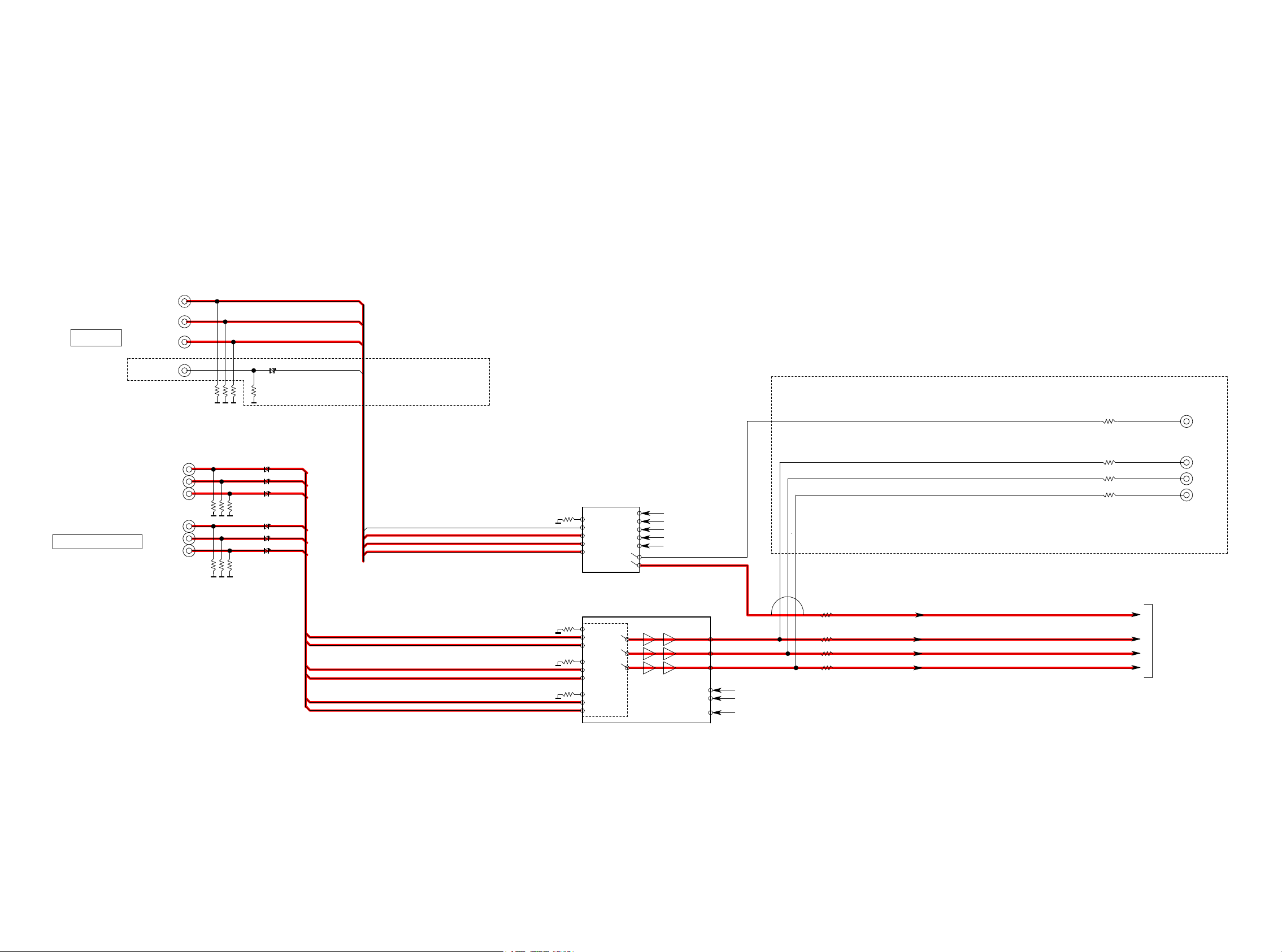
fig.01a
AVR-X3000 ANALOG VIDEO BLOCK
CVBS IN
COMPONENT IN
CBL/SAT
DVD
MEDIA Player
V.AUX(FRONT)
CBL/SAT
DVD
CBL/SAT_V
DVD_V
Blu-Ray_V
V.AUX_V
75
75
not use
not use
CVBS MONITOR
CVBS OUT
COMPONENT OUT Y
CBL/SAT_Y
CBL/SAT_PB
CBL/SAT_PR
DVD_Y
DVD_PB
DVD_PR
CBL/SAT_Y
DVD_Y
CBL/SAT_PB
DVD_PB
CBL/SAT_PR
DVD_PR
V_AUX_V
CBL/SAT_V
DVD_V
Blu-Ray_V
NJM2595MTE1
VO1
VO2
SW1
SW2
SW3
SW4
SW5
VI1
VI2
VI3
VI4
VI5
NJM2586A
CH1 IN1
CH1 IN2
CH1 IN3
CH2 IN1
CH2 IN2
CH2 IN3
CH3 IN1
CH3 IN2
CH3 IN3
DEC_CVBS_IN
CH1 OUT
CH2 OUT
CH3 OUT
SW1
SW2
PS
YOUT
PBOUT
PROUT
75
6dB
75
6dB
75
6dB
DEC_Y_IN
_PB_IN
DEC
DEC_PR_IN
COMPONENT OUT PB
COMPONENT OUT PR
COMPONENT OUT
DEC_CVBS_IN
DEC_Y_IN
DEC_PB_IN
DEC_PR_IN
TO HDMI VIDEO BLOCK
28
Page 29
fig.01b
AVR-X3000 HDMI VIDEO BLOCK
HDMI IN
HDMI FRT IN
(V.AUX)
HDMI IN1
(CBL/SAT)
IN2
HDMI
(DVD)
HDMI IN3
(BLU-RAY)
HDMI IN4
(GAME)
HDMI IN5
(MEDIA PLAYER)
HDMI IN6
(CD)
AD8195
Buffer
SiI9575
SUB
MAIN
WAFER WAFER
FFC
TX_1
TX_0
Port D
Port C
Port B
Port A
DEC_Y_IN
DEC_PB_IN
DEC_PR_IN
DEC_CVBS_IN
VD[0:7]
ADV7850
TMDS INPUT
VIDEO INPUT
27.000MHz
HDMI TX with TMDS
HDMI Rx
ADV8003-3
VIDEO
VIDEO
27MHz
ARC
HDMI OUT1
PROCESSING
VIDEO SIGNAL OUT
AUDIO SIGNAL OUT
CCIR656 VD[0:7]
VIDEO
DIGITAL
DATA
AUDIO
CONTROL
DDR2 INTERFACE
HDMI Tx
HDMI ZONE2
FROM
ANALOG VIDEO BLOCK
FROM
DIGITAL AUDIO BLOCK
27.000MHz
S. FLASH
MX25L12845EMI-10G
9575_SPDIF_OUT
9575_SPDIF_OUT
SN74LVC244APWR
RX_I2S
TX_I2S
128M
DDR2 SDRAM
DDR2 SDRAM
K4T51163QJ-BCE7 K4T51163QJ-BCE7
512M
512M
< TO / FROM
DEC_Y_IN
DEC_PB_IN
DEC_PR_IN
DEC_CVBS_IN
VD[0:7]
DIGITAL AUDIO BLOCK >
29
Page 30
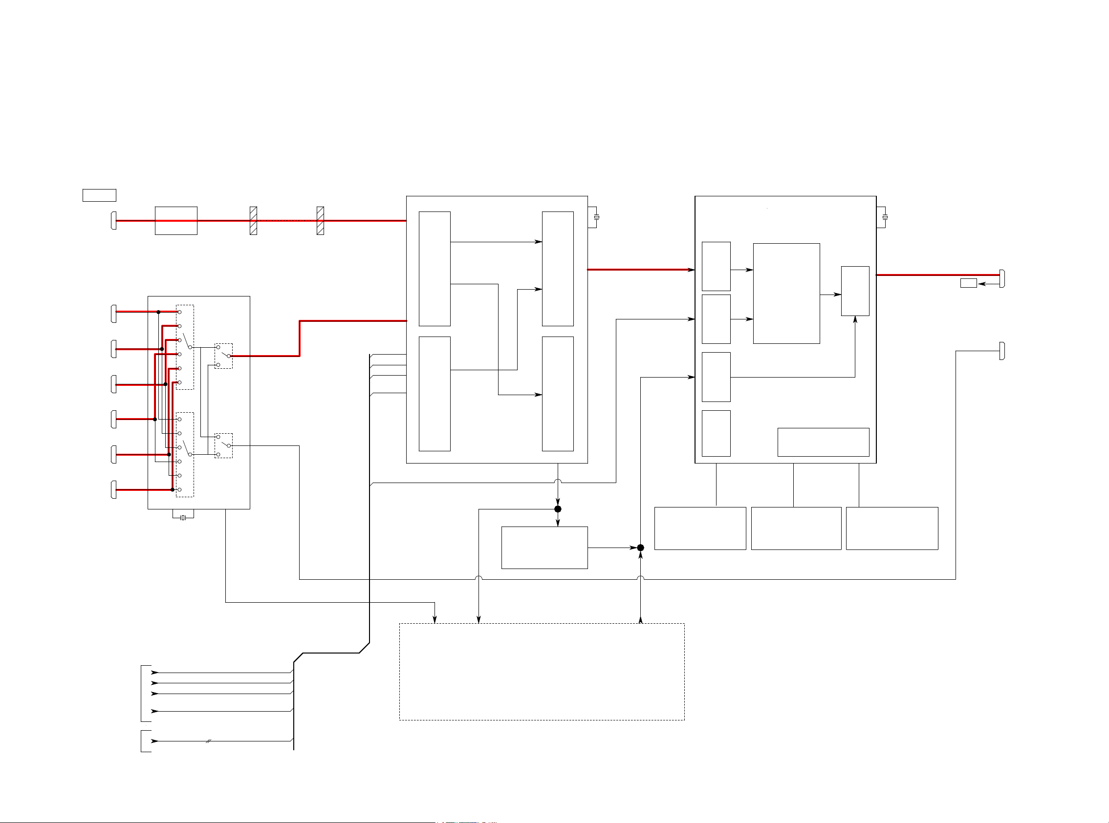
fig.02
AVR-X3000 HDMI VIDEO BLOCK
HDMI IN
HDMI FRT IN
(V.AUX)
HDMI IN1
(CBL/SAT)
HDMI IN2
(DVD)
HDMI IN3
(BLU-RAY)
HDMI IN4
(GAME)
HDMI I
(MEDIA PLAYER)
HDMI IN6
(CD)
WAFER WAFER
AD8195
Buffer
FFC
Port D
ADV7850
27.000MHz
ADV8003-3
27MHz
Port C
HDMI TX with TMDS
VIDEO
PROCESSING
ARC
HDMI OUT1
HDMI Tx
HDMI ZONE2
SiI9575
SUB
TX_1
Port B
Port A
DEC_Y_IN
DEC_PB_IN
DEC_PR_IN
DEC_CVBS_IN
VIDEO
HDMI Rx
TMDS INPUT
VIDEO SIGNAL OUT
CCIR656 VD[0:7]
VIDEO
DIGITAL
DATA
AUDIO
VIDEO INPUT
MAIN
TX_0
N5
VD[0:7]
AUDIO SIGNAL OUT
CONTROL
DDR2 INTERFACE
FROM
ANALOG VIDEO BLOCK
FROM
DIGITAL AUDIO BLOCK
27.000MHz
S. FLASH
MX25L12845EMI-10G
9575_SPDIF_OUT
9575_SPDIF_OUT
SN74LVC244APWR
RX_I2S
TX_I2S
128M
DDR2 SDRAM
DDR2 SDRAM
K4T51163QJ-BCE7 K4T51163QJ-BCE7
512M
512M
< TO / FROM
DEC_Y_IN
DEC_PB_IN
DEC_PR_IN
DEC_CVBS_IN
VD[0:7]
DIGITAL AUDIO BLOCK >
30
Page 31

fig.03
AVR-X3000 HDMI VIDEO BLOCK
HDMI IN
HDMI FRT IN
(V.AUX)
HDMI IN1
(CBL/SAT)
HDMI IN2
(DVD)
HDMI IN3
(BLU-RAY)
HDMI IN4
(GAME)
HDMI I
(MEDIA PLAYER)
HDMI IN6
(CD)
WAFER WAFER
AD8195
Buffer
FFC
Port D
ADV7850
27.000MHz
ADV8003-3
27MHz
Port C
μCOM
ARC
HDMI OUT1
HDMI ZONE2
SiI9575
SUB
TX_1
Port B
Port A
DEC_Y_IN
DEC_PB_IN
DEC_PR_IN
DEC_CVBS_IN
HDMI TX with TMDS
VIDEO
HDMI Rx
TMDS INPUT
VIDEO SIGNAL OUT
CCIR656 VD[0:7]
VIDEO
DIGITAL
DATA
AUDIO
VIDEO
PROCESSING
HDMI Tx
VIDEO INPUT
MAIN
TX_0
N5
VD[0:7]
AUDIO SIGNAL OUT
CONTROL
DDR2 INTERFACE
FROM
ANALOG VIDEO BLOCK
FROM
DIGITAL AUDIO BLOCK
27.000MHz
S. FLASH
MX25L12845EMI-10G
9575_SPDIF_OUT
9575_SPDIF_OUT
SN74LVC244APWR
RX_I2S
TX_I2S
128M
DDR2 SDRAM
DDR2 SDRAM
K4T51163QJ-BCE7 K4T51163QJ-BCE7
512M
512M
< TO / FROM
DEC_Y_IN
DEC_PB_IN
DEC_PR_IN
DEC_CVBS_IN
VD[0:7]
DIGITAL AUDIO BLOCK >
31
Page 32

fig.04a
AVRX3000 DIGITAL AUDIO BLOCK
ADINL
ADINR
DIGTAL IN
OPT1(TV)
OPT2(CD)
COAX1(CBL/SAT)
COAX2(DVD)
FROM HDMI Rx DATA
SPDIF(PCM2ch) I2S(HD Audio)
RXFS
------
RxSD0
------
RxSD1
------
RxSD2
------
RxSD3
------
L/R(to DIR)
RxSPDIF
HDMI IN7
(FRONT)
HDMI IN1
HDMI IN2
HDMI IN3
HDMI IN4
HDMI IN5
HDMI IN6
I2S0
I2S1
I2S2
I2S3
------
------
I2S(PCM Multi) DSD
------
FL/FR
C/SW
SL/SR
SBL/SBR
------
AD8195
SiI9575
O1
O2
C1
C2
FR
FL
C
SL
SR
SW
9575_SPDIF
27.000MHz
HDMISPDIF
RxMCK
RXFS
Rx64FS
RxSD0~3
RxSPDIF
TxMCK
TxFS
Tx64FS
TxSD0~3
TxSPDIF
860_SPDIF
HDMISPDIF
ARCSPDIF1
9575_SPDIF
RXO1
PORT D
PORT C
PORT B
PORT A
C1
C2
O1
O2
860_MCK
ADV7850
HDMI RX
24.576MHz
ADINL
ADINR
ADC+DIR1
PCM9211
256_1
SBCK1
SLRCK1
AUDIO PLD
EPM240T100CN5
BCK
860_
860_DATA
860_LRCK
Z2DIRBCK
Z2DIRMCK
27.000MHz
256FSDIR1
64FSDIR1
FSDIR1
DATADIR1
DIRAMCKI
DIRABCKI
DIRALRCKI
DIRADATAI
Z2DIRDATA
Z2DIRLRCK
RXFS
RxMCK
Rx64FS
DAFL
DAFR
DAC
DAC input DATA
DACDATA
DATAF
DATAC
DATAS
DATASB
FSDIR1
DATADIR1
64FSDIR1
DIRABCKI
DIRAMCKI
Z2DACMCK
RxSPDIF
RxSD0~3
256FSDIR1
DIRADATAI
DIRALRCKI
DACDATA
DAC256FS
DAC64FS
DACFS
DSP1OUTMCK
DSP1OUT64FS
DSP1OUTFS
DSP1OUTF
DSP1OUTCSW
DSP1OUTS
DSP1OUTSB
Z2DACBCK
Z2DACDATA
Z2DACLRCK
TO HDMI Tx DATA
TxFS
TxSD0
TxSD1
TxSD2
TxSD3
TxSPDIF
PCM DATA only
FL/FR
C/SW1
SL/SR
SBL/SBR
DACDATA
DAC256FS
DAC64FS
DACFS
DSP1INMCK
DSP1IN64FS
DSP1INFS
FL/FR_IN(HDMI_I2S_0) // FL_IN(DSD)
C/LFE_IN(HDMI_I2S_1) // C_IN(DSD)
SL/SR_IN(HDMI_I2S_2) // SL_IN(DSD)
SBL/SBR_IN(HDMI_I2S_3) // SR_IN(DSD)
- - - // SW_IN(DSD)
- - - // FR_IN(DSD)
DSP1INLR
256_1
DSP input DATA
FL/FR_IN(HDMI_I2S_0)
C/LFE_IN(HDMI_I2S_1)
SL/SR_IN(HDMI_I2S_2)
L/SBR_IN(HDMI_I2S_3)
SB
SN74LVC244APWR
RxMCK
RXFS
Rx64FS
RxSD0~3
RxSPDIF
SPDIF(PCM2ch) I2S(HD Audio) I2S(PCM Multi) DSD
------
------
------
------
------
L/R(from RX)
OCTAL
BUFFER
------
I2S0
I2S1
I2S2
I2S3
------
TxMCK
TxFS
Tx64FS
TxSD0~3
TxSPDIF
FL/FR
C/SW
SL/SR
SBL/SBR
DAC
PCM1690
DSP
ADSP21487KSWZ-4B
SPDIF(PCM2ch) I2S(HD Audio) I2S(PCM Multi) DSD
L/R_IN
L/R(from DIR)
------
TxMCK
TxFS
Tx64FS
TxSD0~3
TxSPDIF
FR
FL
C
SL
SR
SW
------
------
------
------
------
ARCSPDIF1/2
ADV8003-3
HDMI TX
HDMI Tx
FR_IN(DSD)
LFE_IN(DSD)
------
------
I2S0
I2S1
I2S2
I2S3
------
------
------
27MHz
FLASH SDRAM
------
FL/FR
------
C/SW
------
SL/SR
SBL/SBR
SERIAL FLASH
128M
MX25L12845EMI-10G
DDR2 SDRAM
K4T51163QJ-BCE7
DDR2 SDRAM
K4T51163QJ-BCE7
25MHz
MX29LV160DBTI-70G W9864G6JH-6
512M
512M
Z2DACMCK
Z2DACBCK
Z2DACLRCK
Z2DACDATA
ZONE2
DAC
PCM5100
16M Flash 64M
256_1
Z2DIRMCK
--
FL
FR
C
SW
SL
SR
860_SPDIF
860_MCK
860_BCK
860_LRCK
860_DATA
Z2DIRBCK
Z2DIRLRCK
Z2DIRDATA
LC89091J-H
NETWORK
CONTROLLER
DIR2
RXO1
DM860A_Left Justified
fs/64fs/256fs
24MHz
ESCL/ESDA
USBD-
USBD+
IPOD AUTH.
23671011050AS
(MFI337S3959)
DM860A
VD0~7
VD[0:7]
NAND FLASH
H27U1G8F2BTR-BC
1G
SDRAM
256M
A3V56S30FTP-G6 A 3V56S30FTP-G6
SDRAM
256M
VD[0:7]
MII
ETHERNET
PHY
LAN8720A
TO HDMI VIDEO BLOCK
TD+/-
RX+/-RD+/-
TX+/-
DASW1
DASL
DASR
DASBL
DASBR
DAZ2
RJ-45 with Transformer
TO ANALOG
AUDIO BLOCK
USB
ETHERNET
HDMI ZONE2 OUT
HDMI OUT1
ARC
32
Page 33

fig.04b
FL
FR
CEN
SW
SL
SR
SBL
EXT. INPUT(7.1CH)
SBR
(OPEN)
CBL/SAT
DVD
Blu-Ray
Meadia
CD
PHONO
(OPEN)
V.AUX
ANALOG INPUT
(FRONT)
(OPEN)
AVRX3000:E3 Ver=>SIL TUNER(FM/AM)
AVRX3000:OTHER=>SIL TUNER(FM)
MIC(Mini Jack)
EXTFL
EXTFR
EXTC
EXTSW
EXTSL
EXTSR
EXTSBL
EXTSBR
AZ4580
AZ4580
TUNER
CBL/SAT
DVD
Blu-Ray
Meadia
PHONO
V.AUX
TUNER
MIC
AVRX3000 ANALOG AUDIO BLOCK
ATT
HPL
(OPEN)
ANA_FL
DAFL
ANA_FL/FR
DAF
DAZ2
MIC
Pull down
TUNER
Pull down
CBL/SAT
DVD
Blu-ray
Media
CD
Pull down
CD
EUP
IN1
IN2
IN3
IN4
IN5
IN6
IN7
IN8
INA/REC1
IN9
INB/REC2
IN10/REC4
IN11/REC5
ANA_FL/FR
ADINL/R
SUB
MAIN
ZONE2
VOL IC
R2A15218
EXTFL
ANAFR
DAFR
EXTFR
DAC
EXTC
DASW1
EXTSW
DASL
EXTSL
DASR
EXTSR
DASBL
EXTSBL
DASBR
EXTSBR
Z2R
Z2L
TONE
TONE
SW1
FL
CEN
SL
SR
SBL
SBR
AMPFL
AMPFR
FR
MAIN AMP
2SD2560/2SB1647
AMPC
AMPSL
AMPSR
AMPSBL
AMPSBR
GND
HPR
+
FL
-
+
FR
-
+
F_L
-
assignable
+
F_R
-
(OPEN)
+
C
-
+
SL
-
+
SR
-
+
SBL
-
+
SBR
-
H/P OUTSPK OUT_A
SPK OUT_B
SPK OUT
MX PORT
TO DIGITAL
AUDIO BLOCK
DAZ2
ADFL
ADFR
DAFL
DAFR
DACEN
DASW1
DASL
DASR
DASBL
DASBR
(OPEN)
MXP
ADINL
ADINR
DAFL
DAFR
DAC
DASW1
DASL
DASR
DASBL
DASBR
MUTE
MUTE
EXCEPT E3
FL
FR
C
SL
SR
SBL
SBR
SW1
SW2
ZONE2 OUT
PRE OUT
PREFL
PREFR
Z2L
HPF
MONO
MIX
Z2R
HPF
MONO
MIX
VOL IC
NJW1194V
ZONE2_L
ZONE2
ZONE2_R
PREC
PRESL
PRESR
PRESBL
PRESBR
MUTE
MUTE
MUTE
MUTE
MUTE
MUTE
MUTE
PRESW1
PRESW2
ZONE2_L/R
MUTE
33
Page 34

fig.05
AVRX3000 DIGITAL AUDIO BLOCK
ADINL
ADINR
DIGTAL IN
OPT1(TV)
OPT2(CD)
COAX1(CBL/SAT)
COAX2(DVD)
FROM HDMI Rx DATA
SPDIF(PCM2ch) I2S(HD Audio) I2S(PCM Multi) DSD
RXFS
RxSD0
RxSD1
RxSD2
RxSD3
RxSPDIF
------
------
------
------
------
L/R(to DIR)
HDMI IN7
(FRONT)
I2S0
I2S1
I2S2
I2S3
------
------
HDMI IN1
HDMI IN2
HDMI IN3
HDMI IN4
HDMI IN5
HDMI IN6
------
FL/FR
C/SW
SL/SR
SBL/SBR
------
AD8195
SiI9575
O1
O2
C1
C2
FR
FL
C
SL
SR
SW
9575_SPDIF
27.000MHz
HDMISPDIF
RxMCK
RXFS
Rx64FS
~3
RxSD0
RxSPDIF
TxMCK
TxFS
Tx64FS
TxSD0~3
TxSPDIF
860_SPDIF
HDMISPDIF
ARCSPDIF1
9575_SPDIF
RXO1
PORT D
PORT C
PORT B
PORT A
C1
C2
O1
O2
860_MCK
ADV7850
HDMI RX
24.576MHz
ADINL
ADINR
ADC+DIR1
PCM9211
256_1
SBCK1
SLRCK1
AUDIO PLD
EPM240T100CN5
Z2DIRBCK
860_BCK
860_LRCK
Z2DIRMCK
860_DATA
27.000MHz
256FSDIR1
64FSDIR1
FSDIR1
DATADIR1
DIRAMCKI
DIRABCKI
DIRALRCKI
DIRADATAI
Z2DIRDATA
Z2DIRLRCK
RXFS
RxMCK
Rx64FS
DAFL
DAFR
DAC
DAC input DATA
DACDATA
DATAF
DATAC
DATAS
DATASB
FSDIR1
DATADIR1
64FSDIR1
DIRABCKI
DIRAMCKI
Z2DACMCK
RxSPDIF
RxSD0~3
256FSDIR1
DIRADATAI
DIRALRCKI
DACDATA
DAC256FS
DAC64FS
DACFS
DSP1OUTMCK
DSP1OUT64FS
DSP1OUTFS
DSP1OUTF
DSP1OUT
DSP1OUTS
DSP1OUTSB
Z2DACBCK
Z2DACDATA
Z2DACLRCK
TO HDMI Tx DATA
TxFS
TxSD0
TxSD1
TxSD2
TxSD3
TxSPDIF
PCM DATA only
FL/FR
C/SW1
SL/SR
SBL/SBR
DACDATA
DAC256FS
DAC64FS
DACFS
CSW
DSP1INMCK
DSP1IN64FS
DSP1INFS
FL/FR_IN(HDMI_I2S_0) // FL_IN(DSD)
C/LFE_IN(HDMI_I2S_1) // C_IN(DSD)
SL/SR_IN(HDMI_I2S_2) // SL_IN(DSD)
SBL/SBR_IN(HDMI_I2S_3) // SR_IN(DSD)
- - - // SW_IN(DSD)
- - - // FR_IN(DSD)
DSP1INLR
256_1
DSP input DATA
FL/FR_IN(HDMI_I2S_0)
C/LFE_IN(HDMI_I2S_1)
SL/SR_IN(HDMI_I2S_2)
SBL/SBR_IN(HDMI_I2S_3)
SN74LVC244APWR
RxMCK
RXFS
Rx64FS
RxSD0~3
RxSPDIF
SPDIF(PCM2ch) I2S(HD Audio) I2S(PCM Multi) DSD
------
------
------
------
------
L/R(from RX)
OCTAL
BUFFER
------
I2S0
I2S1
I2S2
I2S3
------
TxMCK
TxFS
Tx64FS
TxSD0~3
TxSPDIF
FL/FR
C/SW
SL/SR
SBL/SBR
DAC
PCM1690
DSP
ADSP21487KSWZ-4B
SPDIF(PCM2ch) I2S(HD Audio) I2S(PCM Multi) DSD
L/R_IN
L/R(from DIR)
------
TxMCK
TxFS
Tx64FS
TxSD0~3
TxSPDIF
FR
FL
C
SL
SR
SW
------
------
------
------
------
ARCSPDIF1/2
ADV8003-3
HDMI TX
HDMI Tx
FR_IN(DSD)
LFE_IN(DSD)
------
------
I2S0
I2S1
I2S2
I2S3
------
------
------
27MHz
FLASH SDRAM
------
FL/FR
------
C/SW
------
SL/SR
SBL/SBR
SERIAL FLASH
128M
MX25L12845EMI-10G
DDR2 SDRAM
K4T51163QJ-BCE7
DDR2 SDRAM
K4T51163QJ-BCE7
25MHz
MX29LV160DBTI-70G W9864G6JH-6
512M
512M
Z2DACMCK
Z2DACBCK
Z2DACLRCK
Z2DACDATA
ZONE2
DAC
PCM5100
16M Flash 64M
256_1
Z2DIRMCK
--
FL
FR
C
SW
SL
SR
860_SPDIF
860_MCK
860_BCK
860_LRCK
860_DATA
Z2DIRBCK
Z2DIRLRCK
Z2DIRDATA
LC89091J-H
NETWORK
CONTROLLER
DIR2
RXO1
DM860A_Left Justified
fs/64fs/256fs
24MHz
ESCL/ESDA
USBD-
USBD+
IPOD AUTH.
23671011050AS
(MFI337S3959)
DM860A
VD0~7
VD[0:7]
NAND FLASH
H27U1G8F2BTR-BC
1G
SDRAM
256M
A3V56S30FTP-G6 A 3V56S30FTP-G6
SDRAM
256M
VD[0:7]
MII
ETHERNET
PHY
LAN8720A
TO HDMI VIDEO BLOCK
TD+/-
RX+/-RD+/-
TX+/-
DASW1
DASL
DASR
DASBL
DASBR
DAZ2
RJ-45 with Transformer
TO ANALOG
AUDIO BLOCK
USB
ETHERNET
HDMI ZONE2 OUT
HDMI OUT1
ARC
34
Page 35

fig.06
AVR-X3000 HDMI VIDEO BLOCK
HDMI IN
HDMI FRT IN
(V.AUX)
HDMI IN1
(CBL/SAT)
HDMI IN2
(DVD)
HDMI IN3
(BLU-RAY)
HDMI IN4
(GAME)
HDMI I
(MEDIA PLAYER)
HDMI IN6
(CD)
WAFER WAFER
AD8195
Buffer
FFC
Port D
ADV7850
27.000MHz
ADV8003-3
27MHz
Port C
HDMI TX with TMDS
VIDEO
PROCESSING
ARC
HDMI OUT1
HDMI Tx
HDMI ZONE2
SiI9575
SUB
TX_1
Port B
Port A
DEC_Y_IN
DEC_PB_IN
DEC_PR_IN
DEC_CVBS_IN
VIDEO
HDMI Rx
TMDS INPUT
VIDEO SIGNAL OUT
CCIR656 VD[0:7]
VIDEO
DIGITAL
DATA
AUDIO
VIDEO INPUT
MAIN
TX_0
N5
VD[0:7]
AUDIO SIGNAL OUT
CONTROL
DDR2 INTERFACE
FROM
ANALOG VIDEO BLOCK
FROM
DIGITAL AUDIO BLOCK
27.000MHz
S. FLASH
MX25L12845EMI-10G
9575_SPDIF_OUT
9575_SPDIF_OUT
SN74LVC244APWR
RX_I2S
TX_I2S
128M
DDR2 SDRAM
DDR2 SDRAM
K4T51163QJ-BCE7 K4T51163QJ-BCE7
512M
512M
< TO / FROM
DEC_Y_IN
DEC_PB_IN
DEC_PR_IN
DEC_CVBS_IN
VD[0:7]
DIGITAL AUDIO BLOCK >
35
Page 36

fig.07
AVR-X3000 HDMI VIDEO BLOCK
HDMI IN
HDMI FRT IN
(V.AUX)
HDMI IN1
(CBL/SAT)
HDMI IN2
(DVD)
HDMI IN3
(BLU-RAY)
HDMI IN4
(GAME)
HDMI IN5
(MEDIA PLAYER)
HDMI IN6
(CD)
AD8195
Buffer
SiI9575
SUB
MAIN
WAFER WAFER
TX_0
Port D
Port C
Port B
Port A
DEC_Y_IN
DEC_PB_IN
DEC_PR_IN
DEC_CVBS_IN
VD[0:7]
ADV7850
TMDS INPUT
VIDEO INPUT
27.000MHz
HDMI TX with TMDS
HDMI Rx
ADV8003-3
VIDEO
VIDEO
PROCESSING
VIDEO SIGNAL OUT
AUDIO SIGNAL OUT
CCIR656 VD[0:7]
VIDEO
DIGITAL
DATA
AUDIO
CONTROL
DDR2 INTERFACE
HDMI Tx
27MHz
ARC
HDMI OUT1
HDMI ZONE2
FROM
ANALOG VIDEO BLOCK
FROM
DIGITAL AUDIO BLOCK
27.000MHz
S. FLASH
MX25L12845EMI-10G
9575_SPDIF_OUT
9575_SPDIF_OUT
SN74LVC244APWR
RX_I2S
TX_I2S
128M
DDR2 SDRAM
DDR2 SDRAM
K4T51163QJ-BCE7 K4T51163QJ-BCE7
512M
512M
< TO / FROM
DEC_Y_IN
DEC_PB_IN
DEC_PR_IN
DEC_CVBS_IN
VD[0:7]
DIGITAL AUDIO BLOCK >
36
Page 37

fig.08
FL
FR
CEN
SW
SL
SR
SBL
EXT. INPUT(7.1CH)
SBR
(OPEN)
CBL/SAT
DVD
Blu-Ray
Meadia
CD
PHONO
(OPEN)
V.AUX
ANALOG INPUT
(FRONT)
(OPEN)
AVRX3000:E3 Ver=>SIL TUNER(FM/AM)
AVRX3000:OTHER=>SIL TUNER(FM)
MIC(Mini Jack)
EXTFL
EXTFR
EXTC
EXTSW
EXTSL
EXTSR
EXTSBL
EXTSBR
AZ4580
AZ4580
TUNER
CBL/SAT
DVD
Blu-Ray
Meadia
PHONO
V.AUX
TUNER
MIC
AVRX3000 ANALOG AUDIO BLOCK
ATT
HPL
(OPEN)
ANA_FL
DAFL
ANA_FL/FR
DAF
DAZ2
MIC
Pull down
TUNER
Pull down
CBL/SAT
DVD
Blu-ray
Media
CD
Pull down
CD
EUP
IN1
IN2
IN3
IN4
IN5
IN6
IN7
IN8
INA/REC1
IN9
INB/REC2
IN10/REC4
IN11/REC5
ANA_FL/FR
ADINL/R
SUB
MAIN
ZONE2
VOL IC
R2A15218
EXTFL
ANAFR
DAFR
EXTFR
DAC
EXTC
DASW1
EXTSW
DASL
EXTSL
DASR
EXTSR
DASBL
EXTSBL
DASBR
EXTSBR
Z2R
Z2L
TONE
TONE
SW1
FL
CEN
SL
SR
SBL
SBR
AMPFL
AMPFR
FR
MAIN AMP
2SD2560/2SB1647
AMPC
AMPSL
AMPSR
AMPSBL
AMPSBR
GND
HPR
+
FL
-
+
FR
-
+
F_L
-
assignable
+
F_R
-
(OPEN)
+
C
-
+
SL
-
+
SR
-
+
SBL
-
+
SBR
-
H/P OUTSPK OUT_A
SPK OUT_B
SPK OUT
MX PORT
TO DIGITAL
AUDIO BLOCK
DAZ2
ADFL
ADFR
DAFL
DAFR
DACEN
DASW1
DASL
DASR
DASBL
DASBR
(OPEN)
MXP
ADINL
ADINR
DAFL
DAFR
DAC
DASW1
DASL
DASR
DASBL
DASBR
MUTE
MUTE
EXCEPT E3
FL
FR
C
SL
SR
SBL
SBR
SW1
SW2
ZONE2 OUT
PRE OUT
PREFL
PREFR
Z2L
HPF
MONO
MIX
Z2R
HPF
MONO
MIX
VOL IC
NJW1194V
ZONE2_L
ZONE2
ZONE2_R
PREC
PRESL
PRESR
PRESBL
PRESBR
MUTE
MUTE
MUTE
MUTE
MUTE
MUTE
MUTE
PRESW1
PRESW2
ZONE2_L/R
MUTE
37
Page 38

fig.09a
FL
FR
CEN
SW
SL
SR
SBL
EXT. INPUT(7.1CH)
SBR
(OPEN)
CBL/SAT
DVD
Blu-Ray
Meadia
CD
PHONO
(OPEN)
V.AUX
ANALOG INPUT
(FRONT)
(OPEN)
AVRX3000:E3 Ver=>SIL TUNER(FM/AM)
AVRX3000:OTHER=>SIL TUNER(FM)
MIC(Mini Jack)
EXTFL
EXTFR
EXTC
EXTSW
EXTSL
EXTSR
EXTSBL
EXTSBR
AZ4580
AZ4580
TUNER
CBL/SAT
DVD
Blu-Ray
Meadia
PHONO
V.AUX
TUNER
MIC
AVRX3000 ANALOG AUDIO BLOCK
ATT
HPL
(OPEN)
ANA_FL
DAFL
ANA_FL/FR
DAF
DAZ2
MIC
Pull down
TUNER
Pull down
CBL/SAT
DVD
Blu-ray
Media
CD
Pull down
CD
EUP
IN1
IN2
IN3
IN4
IN5
IN6
IN7
IN8
INA/REC1
IN9
INB/REC2
IN10/REC4
IN11/REC5
ANA_FL/FR
ADINL/R
SUB
MAIN
ZONE2
VOL IC
R2A15218
EXTFL
ANAFR
DAFR
EXTFR
DAC
EXTC
DASW1
EXTSW
DASL
EXTSL
DASR
EXTSR
DASBL
EXTSBL
DASBR
EXTSBR
Z2R
Z2L
TONE
TONE
SW1
FL
CEN
SL
SR
SBL
SBR
AMPFL
AMPFR
FR
MAIN AMP
2SD2560/2SB1647
AMPC
AMPSL
AMPSR
AMPSBL
AMPSBR
GND
HPR
+
FL
-
+
FR
-
+
F_L
-
assignable
+
F_R
-
(OPEN)
+
C
-
+
SL
-
+
SR
-
+
SBL
-
+
SBR
-
H/P OUTSPK OUT_A
SPK OUT_B
SPK OUT
MX PORT
TO DIGITAL
AUDIO BLOCK
DAZ2
ADFL
ADFR
DAFL
DAFR
DACEN
DASW1
DASL
DASR
DASBL
DASBR
(OPEN)
MXP
ADINL
ADINR
DAFL
DAFR
DAC
DASW1
DASL
DASR
DASBL
DASBR
MUTE
MUTE
EXCEPT E3
FL
FR
C
SL
SR
SBL
SBR
SW1
SW2
ZONE2 OUT
PRE OUT
PREFL
PREFR
Z2L
HPF
MONO
MIX
Z2R
HPF
MONO
MIX
VOL IC
NJW1194V
ZONE2_L
ZONE2
ZONE2_R
PREC
PRESL
PRESR
PRESBL
PRESBR
MUTE
MUTE
MUTE
MUTE
MUTE
MUTE
MUTE
PRESW1
PRESW2
ZONE2_L/R
MUTE
38
Page 39

fig.09b
AVRX3000 DIGITAL AUDIO BLOCK
ADINL
ADINR
DIGTAL IN
OPT1(TV)
OPT2(CD)
COAX1(CBL/SAT)
COAX2(DVD)
FROM HDMI Rx DATA
SPDIF(PCM2ch) I2S(HD Audio) I2S(PCM Multi) DSD
RXFS
RxSD0
RxSD1
RxSD2
RxSD3
RxSPDIF
------
------
------
------
------
L/R(to DIR)
HDMI IN7
(FRONT)
I2S0
I2S1
I2S2
I2S3
------
------
HDMI IN1
HDMI IN2
HDMI IN3
HDMI IN4
HDMI IN5
HDMI IN6
------
FL/FR
C/SW
SL/SR
SBL/SBR
------
AD8195
SiI9575
O1
O2
C1
C2
FR
FL
C
SL
SR
SW
9575_SPDIF
27.000MHz
HDMISPDIF
RxMCK
RXFS
Rx64FS
~3
RxSD0
RxSPDIF
TxMCK
TxFS
Tx64FS
TxSD0~3
TxSPDIF
860_SPDIF
HDMISPDIF
ARCSPDIF1
9575_SPDIF
RXO1
PORT D
PORT C
PORT B
PORT A
C1
C2
O1
O2
860_MCK
ADV7850
HDMI RX
24.576MHz
ADINL
ADINR
ADC+DIR1
PCM9211
256_1
SBCK1
SLRCK1
AUDIO PLD
EPM240T100CN5
Z2DIRBCK
860_BCK
860_LRCK
Z2DIRMCK
860_DATA
27.000MHz
256FSDIR1
64FSDIR1
FSDIR1
DATADIR1
DIRAMCKI
DIRABCKI
DIRALRCKI
DIRADATAI
Z2DIRDATA
Z2DIRLRCK
RXFS
RxMCK
DAFL
DAFR
DAC
DAC input DATA
DACDATA
DATAF
DATAC
DATAS
DATASB
FSDIR1
DATADIR1
64FSDIR1
DIRABCKI
DIRAMCKI
Z2DACMCK
Rx64FS
RxSPDIF
RxSD0~3
256FSDIR1
DIRADATAI
DIRALRCKI
DACDATA
DAC256FS
DAC64FS
DACFS
DSP1OUTMCK
DSP1OUT64FS
DSP1OUTFS
DSP1OUTF
DSP1OUT
DSP1OUTS
DSP1OUTSB
Z2DACBCK
Z2DACDATA
Z2DACLRCK
TO HDMI Tx DATA
TxFS
TxSD0
TxSD1
TxSD2
TxSD3
TxSPDIF
PCM DATA only
FL/FR
C/SW1
SL/SR
SBL/SBR
DACDATA
DAC256FS
DAC64FS
DACFS
CSW
DSP1INMCK
DSP1IN64FS
DSP1INFS
FL/FR_IN(HDMI_I2S_0) // FL_IN(DSD)
C/LFE_IN(HDMI_I2S_1) // C_IN(DSD)
SL/SR_IN(HDMI_I2S_2) // SL_IN(DSD)
SBL/SBR_IN(HDMI_I2S_3) // SR_IN(DSD)
- - - // SW_IN(DSD)
- - - // FR_IN(DSD)
DSP1INLR
256_1
DSP input DATA
FL/FR_IN(HDMI_I2S_0)
C/LFE_IN(HDMI_I2S_1)
SL/SR_IN(HDMI_I2S_2)
SBL/SBR_IN(HDMI_I2S_3)
SN74LVC244APWR
RxMCK
RXFS
Rx64FS
RxSD0~3
RxSPDIF
SPDIF(PCM2ch) I2S(HD Audio) I2S(PCM Multi) DSD
------
------
------
------
------
L/R(from RX)
OCTAL
BUFFER
------
I2S0
I2S1
I2S2
I2S3
------
TxMCK
TxFS
Tx64FS
TxSD0~3
TxSPDIF
DAC
PCM1690
DSP
ADSP21487KSWZ-4B
SPDIF(PCM2ch) I2S(HD Audio) I2S(PCM Multi) DSD
L/R_IN
L/R(from DIR)
------
TxMCK
TxFS
Tx64FS
TxSD0~3
TxSPDIF
FR
FL
C
SL
SR
SW
------
------
------
------
------
ARCSPDIF1/2
ADV8003-3
HDMI TX
HDMI Tx
------
FL/FR
C/SW
SL/SR
SBL/SBR
------
FR_IN(DSD)
LFE_IN(DSD)
I2S0
I2S1
I2S2
I2S3
------
------
------
27MHz
FLASH SDRAM
------
FL/FR
------
C/SW
------
SL/SR
SBL/SBR
SERIAL FLASH
128M
MX25L12845EMI-10G
DDR2 SDRAM
K4T51163QJ-BCE7
DDR2 SDRAM
K4T51163QJ-BCE7
25MHz
MX29LV160DBTI-70G W9864G6JH-6
512M
512M
Z2DACMCK
Z2DACBCK
Z2DACLRCK
Z2DACDATA
ZONE2
DAC
PCM5100
16M Flash 64M
256_1
Z2DIRMCK
--
FL
FR
C
SW
SL
SR
860_SPDIF
860_MCK
860_BCK
860_LRCK
860_DATA
Z2DIRBCK
Z2DIRLRCK
Z2DIRDATA
LC89091J-H
NETWORK
CONTROLLER
DIR2
RXO1
DM860A_Left Justified
fs/64fs/256fs
24MHz
ESCL/ESDA
USBD-
USBD+
IPOD AUTH.
23671011050AS
(MFI337S3959)
DM860A
VD[0:7]
VD0~7
NAND FLASH
H27U1G8F2BTR-BC
1G
SDRAM
256M
A3V56S30FTP-G6 A 3V56S30FTP-G6
SDRAM
256M
VD[0:7]
MII
ETHERNET
PHY
LAN8720A
TO HDMI VIDEO BLOCK
TD+/-
RX+/-RD+/-
TX+/-
DASW1
DASL
DASR
DASBL
DASBR
DAZ2
RJ-45 with Transformer
TO ANALOG
AUDIO BLOCK
USB
ETHERNET
HDMI ZONE2 OUT
HDMI OUT1
ARC
39
Page 40

fig.10a
FL
FR
CEN
SW
SL
SR
SBL
EXT. INPUT(7.1CH)
SBR
(OPEN)
CBL/SAT
DVD
Blu-Ray
Meadia
CD
PHONO
(OPEN)
V.AUX
ANALOG INPUT
(FRONT)
(OPEN)
AVRX3000:E3 Ver=>SIL TUNER(FM/AM)
AVRX3000:OTHER=>SIL TUNER(FM)
MIC(Mini Jack)
EXTFL
EXTFR
EXTC
EXTSW
EXTSL
EXTSR
EXTSBL
EXTSBR
AZ4580
AZ4580
TUNER
CBL/SAT
DVD
Blu-Ray
Meadia
PHONO
V.AUX
TUNER
MIC
AVRX3000 ANALOG AUDIO BLOCK
ATT
HPL
(OPEN)
ANA_FL
DAFL
ANA_FL/FR
DAF
DAZ2
MIC
Pull down
TUNER
Pull down
CBL/SAT
DVD
Blu-ray
Media
CD
Pull down
CD
EUP
IN1
IN2
IN3
IN4
IN5
IN6
IN7
IN8
INA/REC1
IN9
INB/REC2
IN10/REC4
IN11/REC5
ANA_FL/FR
ADINL/R
SUB
MAIN
ZONE2
VOL IC
R2A15218
EXTFL
ANAFR
DAFR
EXTFR
DAC
EXTC
DASW1
EXTSW
DASL
EXTSL
DASR
EXTSR
DASBL
EXTSBL
DASBR
EXTSBR
Z2R
Z2L
TONE
TONE
SW1
FL
CEN
SL
SR
SBL
SBR
AMPFL
AMPFR
FR
MAIN AMP
2SD2560/2SB1647
AMPC
AMPSL
AMPSR
AMPSBL
AMPSBR
GND
HPR
+
FL
-
+
FR
-
+
F_L
-
assignable
+
F_R
-
(OPEN)
+
C
-
+
SL
-
+
SR
-
+
SBL
-
+
SBR
-
H/P OUTSPK OUT_A
SPK OUT_B
SPK OUT
MX PORT
TO DIGITAL
AUDIO BLOCK
DAZ2
ADFL
ADFR
DAFL
DAFR
DACEN
DASW1
DASL
DASR
DASBL
DASBR
(OPEN)
MXP
ADINL
ADINR
DAFL
DAFR
DAC
DASW1
DASL
DASR
DASBL
DASBR
MUTE
MUTE
EXCEPT E3
FL
FR
C
SL
SR
SBL
SBR
SW1
SW2
ZONE2 OUT
PRE OUT
PREFL
PREFR
Z2L
HPF
MONO
MIX
Z2R
HPF
MONO
MIX
VOL IC
NJW1194V
ZONE2_L
ZONE2
ZONE2_R
PREC
PRESL
PRESR
PRESBL
PRESBR
MUTE
MUTE
MUTE
MUTE
MUTE
MUTE
MUTE
PRESW1
PRESW2
ZONE2_L/R
MUTE
40
Page 41

fig.10b
AVRX3000 DIGITAL AUDIO BLOCK
ADINL
ADINR
DIGTAL IN
OPT1(TV)
OPT2(CD)
COAX1(CBL/SAT)
COAX2(DVD)
FROM HDMI Rx DATA
SPDIF(PCM2ch) I2S(HD Audio) I2S(PCM Multi) DSD
RXFS
RxSD0
RxSD1
RxSD2
RxSD3
RxSPDIF
------
------
------
------
------
L/R(to DIR)
HDMI IN7
(FRONT)
I2S0
I2S1
I2S2
I2S3
------
------
HDMI IN1
HDMI IN2
HDMI IN3
HDMI IN4
HDMI IN5
HDMI IN6
------
FL/FR
C/SW
SL/SR
SBL/SBR
------
AD8195
SiI9575
O1
O2
C1
C2
FR
FL
C
SL
SR
SW
9575_SPDIF
27.000MHz
HDMISPDIF
RxMCK
RXFS
Rx64FS
~3
RxSD0
RxSPDIF
TxMCK
TxFS
Tx64FS
TxSD0~3
TxSPDIF
860_SPDIF
HDMISPDIF
ARCSPDIF1
9575_SPDIF
RXO1
PORT D
PORT C
PORT B
PORT A
C1
C2
O1
O2
860_MCK
ADV7850
HDMI RX
24.576MHz
ADINL
ADINR
ADC+DIR1
PCM9211
256_1
SBCK1
SLRCK1
AUDIO PLD
EPM240T100CN5
Z2DIRBCK
860_BCK
860_LRCK
Z2DIRMCK
860_DATA
27.000MHz
256FSDIR1
64FSDIR1
FSDIR1
DATADIR1
DIRAMCKI
DIRABCKI
DIRALRCKI
DIRADATAI
Z2DIRDATA
Z2DIRLRCK
RXFS
RxMCK
DAFL
DAFR
DAC
DAC input DATA
DACDATA
DATAF
DATAC
DATAS
DATASB
FSDIR1
DATADIR1
64FSDIR1
DIRABCKI
DIRAMCKI
Z2DACMCK
Rx64FS
RxSPDIF
RxSD0~3
256FSDIR1
DIRADATAI
DIRALRCKI
DACDATA
DAC256FS
DAC64FS
DACFS
DSP1OUTMCK
DSP1OUT64FS
DSP1OUTFS
DSP1OUTF
DSP1OUT
DSP1OUTS
DSP1OUTSB
Z2DACBCK
Z2DACDATA
Z2DACLRCK
TO HDMI Tx DATA
TxFS
TxSD0
TxSD1
TxSD2
TxSD3
TxSPDIF
PCM DATA only
FL/FR
C/SW1
SL/SR
SBL/SBR
DACDATA
DAC256FS
DAC64FS
DACFS
CSW
DSP1INMCK
DSP1IN64FS
DSP1INFS
FL/FR_IN(HDMI_I2S_0) // FL_IN(DSD)
C/LFE_IN(HDMI_I2S_1) // C_IN(DSD)
SL/SR_IN(HDMI_I2S_2) // SL_IN(DSD)
SBL/SBR_IN(HDMI_I2S_3) // SR_IN(DSD)
- - - // SW_IN(DSD)
- - - // FR_IN(DSD)
DSP1INLR
256_1
DSP input DATA
FL/FR_IN(HDMI_I2S_0)
C/LFE_IN(HDMI_I2S_1)
SL/SR_IN(HDMI_I2S_2)
SBL/SBR_IN(HDMI_I2S_3)
SN74LVC244APWR
RxMCK
RXFS
Rx64FS
RxSD0~3
RxSPDIF
SPDIF(PCM2ch) I2S(HD Audio) I2S(PCM Multi) DSD
------
------
------
------
------
L/R(from RX)
OCTAL
BUFFER
------
I2S0
I2S1
I2S2
I2S3
------
TxMCK
TxFS
Tx64FS
TxSD0~3
TxSPDIF
DAC
PCM1690
DSP
ADSP21487KSWZ-4B
SPDIF(PCM2ch) I2S(HD Audio) I2S(PCM Multi) DSD
L/R_IN
L/R(from DIR)
------
TxMCK
TxFS
Tx64FS
TxSD0~3
TxSPDIF
FR
FL
C
SL
SR
SW
------
------
------
------
------
ARCSPDIF1/2
ADV8003-3
HDMI TX
HDMI Tx
------
FL/FR
C/SW
SL/SR
SBL/SBR
------
FR_IN(DSD)
LFE_IN(DSD)
I2S0
I2S1
I2S2
I2S3
------
------
------
27MHz
FLASH SDRAM
------
FL/FR
------
C/SW
------
SL/SR
SBL/SBR
SERIAL FLASH
128M
MX25L12845EMI-10G
DDR2 SDRAM
K4T51163QJ-BCE7
DDR2 SDRAM
K4T51163QJ-BCE7
25MHz
MX29LV160DBTI-70G W9864G6JH-6
512M
512M
Z2DACMCK
Z2DACBCK
Z2DACLRCK
Z2DACDATA
ZONE2
DAC
PCM5100
16M Flash 64M
256_1
Z2DIRMCK
--
FL
FR
C
SW
SL
SR
860_SPDIF
860_MCK
860_BCK
860_LRCK
860_DATA
Z2DIRBCK
Z2DIRLRCK
Z2DIRDATA
LC89091J-H
NETWORK
CONTROLLER
DIR2
RXO1
DM860A_Left Justified
fs/64fs/256fs
24MHz
ESCL/ESDA
USBD-
USBD+
IPOD AUTH.
23671011050AS
(MFI337S3959)
DM860A
VD[0:7]
VD0~7
NAND FLASH
H27U1G8F2BTR-BC
1G
SDRAM
256M
A3V56S30FTP-G6 A 3V56S30FTP-G6
SDRAM
256M
VD[0:7]
MII
ETHERNET
PHY
LAN8720A
TO HDMI VIDEO BLOCK
TD+/-
DASW1
DASL
DASR
DASBL
DASBR
DAZ2
RX+/-RD+/-
TX+/-
RJ-45 with Transformer
TO ANALOG
AUDIO BLOCK
USB
ETHERNET
HDMI ZONE2 OUT
HDMI OUT1
ARC
41
Page 42

fig.11a
FL
FR
CEN
SW
SL
SR
SBL
EXT. INPUT(7.1CH)
SBR
(OPEN)
CBL/SAT
DVD
Blu-Ray
Meadia
CD
PHONO
(OPEN)
V.AUX
ANALOG INPUT
(FRONT)
(OPEN)
AVRX3000:E3 Ver=>SIL TUNER(FM/AM)
AVRX3000:OTHER=>SIL TUNER(FM)
MIC(Mini Jack)
EXTFL
EXTFR
EXTC
EXTSW
EXTSL
EXTSR
EXTSBL
EXTSBR
AZ4580
AZ4580
TUNER
CBL/SAT
DVD
Blu-Ray
Meadia
PHONO
V.AUX
TUNER
MIC
AVRX3000 ANALOG AUDIO BLOCK
ATT
HPL
(OPEN)
ANA_FL
DAFL
ANA_FL/FR
DAF
DAZ2
MIC
Pull down
TUNER
Pull down
CBL/SAT
DVD
Blu-ray
Media
CD
Pull down
CD
EUP
IN1
IN2
IN3
IN4
IN5
IN6
IN7
IN8
INA/REC1
IN9
INB/REC2
IN10/REC4
IN11/REC5
ANA_FL/FR
ADINL/R
SUB
MAIN
ZONE2
VOL IC
R2A15218
EXTFL
ANAFR
DAFR
EXTFR
DAC
EXTC
DASW1
EXTSW
DASL
EXTSL
DASR
EXTSR
DASBL
EXTSBL
DASBR
EXTSBR
Z2R
Z2L
TONE
TONE
SW1
FL
CEN
SL
SR
SBL
SBR
AMPFL
AMPFR
FR
MAIN AMP
2SD2560/2SB1647
AMPC
AMPSL
AMPSR
AMPSBL
AMPSBR
GND
HPR
+
FL
-
+
FR
-
+
F_L
-
assignable
+
F_R
-
(OPEN)
+
C
-
+
SL
-
+
SR
-
+
SBL
-
+
SBR
-
H/P OUTSPK OUT_A
SPK OUT_B
SPK OUT
MX PORT
TO DIGITAL
AUDIO BLOCK
DAZ2
ADFL
ADFR
DAFL
DAFR
DACEN
DASW1
DASL
DASR
DASBL
DASBR
(OPEN)
MXP
ADINL
ADINR
DAFL
DAFR
DAC
DASW1
DASL
DASR
DASBL
DASBR
MUTE
MUTE
EXCEPT E3
FL
FR
C
SL
SR
SBL
SBR
SW1
SW2
ZONE2 OUT
PRE OUT
PREFL
PREFR
Z2L
HPF
MONO
MIX
Z2R
HPF
MONO
MIX
VOL IC
NJW1194V
ZONE2_L
ZONE2
ZONE2_R
PREC
PRESL
PRESR
PRESBL
PRESBR
MUTE
MUTE
MUTE
MUTE
MUTE
MUTE
MUTE
PRESW1
PRESW2
ZONE2_L/R
MUTE
42
Page 43

fig.11b
AVRX3000 DIGITAL AUDIO BLOCK
ADINL
ADINR
DIGTAL IN
OPT1(TV)
OPT2(CD)
COAX1(CBL/SAT)
COAX2(DVD)
FROM HDMI Rx DATA
SPDIF(PCM2ch) I2S(HD Audio) I2S(PCM Multi) DSD
RXFS
RxSD0
RxSD1
RxSD2
RxSD3
RxSPDIF
------
------
------
------
------
L/R(to DIR)
HDMI IN7
(FRONT)
I2S0
I2S1
I2S2
I2S3
------
------
HDMI IN1
HDMI IN2
HDMI IN3
HDMI IN4
HDMI IN5
HDMI IN6
------
FL/FR
C/SW
SL/SR
SBL/SBR
------
AD8195
SiI9575
O1
O2
C1
C2
FR
FL
C
SL
SR
SW
9575_SPDIF
27.000MHz
HDMISPDIF
RxMCK
RXFS
Rx64FS
~3
RxSD0
RxSPDIF
TxMCK
TxFS
Tx64FS
TxSD0~3
TxSPDIF
860_SPDIF
HDMISPDIF
ARCSPDIF1
9575_SPDIF
RXO1
PORT D
PORT C
PORT B
PORT A
C1
C2
O1
O2
860_MCK
ADV7850
HDMI RX
24.576MHz
ADINL
ADINR
ADC+DIR1
PCM9211
256_1
SBCK1
SLRCK1
AUDIO PLD
EPM240T100CN5
Z2DIRBCK
860_BCK
860_LRCK
Z2DIRMCK
860_DATA
27.000MHz
256FSDIR1
64FSDIR1
FSDIR1
DATADIR1
DIRAMCKI
DIRABCKI
DIRALRCKI
DIRADATAI
Z2DIRDATA
Z2DIRLRCK
RXFS
RxMCK
DAFL
DAFR
DAC
DAC input DATA
DACDATA
DATAF
DATAC
DATAS
DATASB
FSDIR1
DATADIR1
64FSDIR1
DIRABCKI
DIRAMCKI
Z2DACMCK
Rx64FS
RxSPDIF
RxSD0~3
256FSDIR1
DIRADATAI
DIRALRCKI
DACDATA
DAC256FS
DAC64FS
DACFS
DSP1OUTMCK
DSP1OUT64FS
DSP1OUTFS
DSP1OUTF
DSP1OUT
DSP1OUTS
DSP1OUTSB
Z2DACBCK
Z2DACDATA
Z2DACLRCK
TO HDMI Tx DATA
TxFS
TxSD0
TxSD1
TxSD2
TxSD3
TxSPDIF
PCM DATA only
FL/FR
C/SW1
SL/SR
SBL/SBR
DACDATA
DAC256FS
DAC64FS
DACFS
CSW
DSP1INMCK
DSP1IN64FS
DSP1INFS
FL/FR_IN(HDMI_I2S_0) // FL_IN(DSD)
C/LFE_IN(HDMI_I2S_1) // C_IN(DSD)
SL/SR_IN(HDMI_I2S_2) // SL_IN(DSD)
SBL/SBR_IN(HDMI_I2S_3) // SR_IN(DSD)
- - - // SW_IN(DSD)
- - - // FR_IN(DSD)
DSP1INLR
256_1
DSP input DATA
FL/FR_IN(HDMI_I2S_0)
C/LFE_IN(HDMI_I2S_1)
SL/SR_IN(HDMI_I2S_2)
SBL/SBR_IN(HDMI_I2S_3)
SN74LVC244APWR
RxMCK
RXFS
Rx64FS
RxSD0~3
RxSPDIF
SPDIF(PCM2ch) I2S(HD Audio) I2S(PCM Multi) DSD
------
------
------
------
------
L/R(from RX)
OCTAL
BUFFER
------
I2S0
I2S1
I2S2
I2S3
------
TxMCK
TxFS
Tx64FS
TxSD0~3
TxSPDIF
DAC
PCM1690
DSP
ADSP21487KSWZ-4B
SPDIF(PCM2ch) I2S(HD Audio) I2S(PCM Multi) DSD
L/R_IN
L/R(from DIR)
------
TxMCK
TxFS
Tx64FS
TxSD0~3
TxSPDIF
FR
FL
C
SL
SR
SW
------
------
------
------
------
ARCSPDIF1/2
ADV8003-3
HDMI TX
HDMI Tx
------
FL/FR
C/SW
SL/SR
SBL/SBR
------
FR_IN(DSD)
LFE_IN(DSD)
I2S0
I2S1
I2S2
I2S3
------
------
------
27MHz
FLASH SDRAM
------
FL/FR
------
C/SW
------
SL/SR
SBL/SBR
SERIAL FLASH
128M
MX25L12845EMI-10G
DDR2 SDRAM
K4T51163QJ-BCE7
DDR2 SDRAM
K4T51163QJ-BCE7
25MHz
MX29LV160DBTI-70G W9864G6JH-6
512M
512M
Z2DACMCK
Z2DACBCK
Z2DACLRCK
Z2DACDATA
ZONE2
DAC
PCM5100
16M Flash 64M
256_1
Z2DIRMCK
--
FL
FR
C
SW
SL
SR
860_SPDIF
860_MCK
860_BCK
860_LRCK
860_DATA
Z2DIRBCK
Z2DIRLRCK
Z2DIRDATA
LC89091J-H
NETWORK
CONTROLLER
DIR2
RXO1
DM860A_Left Justified
fs/64fs/256fs
24MHz
ESCL/ESDA
USBD-
USBD+
IPOD AUTH.
23671011050AS
(MFI337S3959)
DM860A
VD[0:7]
VD0~7
NAND FLASH
H27U1G8F2BTR-BC
1G
SDRAM
256M
A3V56S30FTP-G6 A 3V56S30FTP-G6
SDRAM
256M
VD[0:7]
MII
ETHERNET
PHY
LAN8720A
TO HDMI VIDEO BLOCK
TD+/-
DASW1
DASL
DASR
DASBL
DASBR
DAZ2
RX+/-RD+/-
TX+/-
RJ-45 with Transformer
TO ANALOG
AUDIO BLOCK
USB
ETHERNET
HDMI ZONE2 OUT
HDMI OUT1
ARC
43
Page 44

fig.12a
FL
FR
CEN
SW
SL
SR
SBL
EXT. INPUT(7.1CH)
SBR
(OPEN)
CBL/SAT
DVD
Blu-Ray
Meadia
CD
PHONO
(OPEN)
V.AUX
ANALOG INPUT
(FRONT)
(OPEN)
AVRX3000:E3 Ver=>SIL TUNER(FM/AM)
AVRX3000:OTHER=>SIL TUNER(FM)
MIC(Mini Jack)
EXTFL
EXTFR
EXTC
EXTSW
EXTSL
EXTSR
EXTSBL
EXTSBR
AZ4580
AZ4580
TUNER
CBL/SAT
DVD
Blu-Ray
Meadia
PHONO
V.AUX
TUNER
MIC
AVRX3000 ANALOG AUDIO BLOCK
ATT
HPL
(OPEN)
ANA_FL
DAFL
ANA_FL/FR
DAF
DAZ2
MIC
Pull down
TUNER
Pull down
CBL/SAT
DVD
Blu-ray
Media
CD
Pull down
CD
EUP
IN1
IN2
IN3
IN4
IN5
IN6
IN7
IN8
INA/REC1
IN9
INB/REC2
IN10/REC4
IN11/REC5
ANA_FL/FR
ADINL/R
SUB
MAIN
ZONE2
VOL IC
R2A15218
EXTFL
ANAFR
DAFR
EXTFR
DAC
EXTC
DASW1
EXTSW
DASL
EXTSL
DASR
EXTSR
DASBL
EXTSBL
DASBR
EXTSBR
Z2R
Z2L
TONE
TONE
SW1
FL
CEN
SL
SR
SBL
SBR
AMPFL
AMPFR
FR
MAIN AMP
2SD2560/2SB1647
AMPC
AMPSL
AMPSR
AMPSBL
AMPSBR
GND
HPR
+
FL
-
+
FR
-
+
F_L
-
assignable
+
F_R
-
(OPEN)
+
C
-
+
SL
-
+
SR
-
+
SBL
-
+
SBR
-
H/P OUTSPK OUT_A
SPK OUT_B
SPK OUT
MX PORT
TO DIGITAL
AUDIO BLOCK
DAZ2
ADFL
ADFR
DAFL
DAFR
DACEN
DASW1
DASL
DASR
DASBL
DASBR
(OPEN)
MXP
ADINL
ADINR
DAFL
DAFR
DAC
DASW1
DASL
DASR
DASBL
DASBR
MUTE
MUTE
EXCEPT E3
FL
FR
C
SL
SR
SBL
SBR
SW1
SW2
ZONE2 OUT
PRE OUT
PREFL
PREFR
Z2L
HPF
MONO
MIX
Z2R
HPF
MONO
MIX
VOL IC
NJW1194V
ZONE2_L
ZONE2
ZONE2_R
PREC
PRESL
PRESR
PRESBL
PRESBR
MUTE
MUTE
MUTE
MUTE
MUTE
MUTE
MUTE
PRESW1
PRESW2
ZONE2_L/R
MUTE
44
Page 45

fig.12b
AVRX3000 DIGITAL AUDIO BLOCK
ADINL
ADINR
DIGTAL IN
OPT1(TV)
OPT2(CD)
COAX1(CBL/SAT)
COAX2(DVD)
FROM HDMI Rx DATA
SPDIF(PCM2ch) I2S(HD Audio) I2S(PCM Multi) DSD
RXFS
RxSD0
RxSD1
RxSD2
RxSD3
RxSPDIF
------
------
------
------
------
L/R(to DIR)
HDMI IN7
(FRONT)
I2S0
I2S1
I2S2
I2S3
------
------
HDMI IN1
HDMI IN2
HDMI IN3
HDMI IN4
HDMI IN5
HDMI IN6
------
FL/FR
C/SW
SL/SR
SBL/SBR
------
AD8195
SiI9575
O1
O2
C1
C2
FR
FL
C
SL
SR
SW
9575_SPDIF
27.000MHz
HDMISPDIF
RxMCK
RXFS
Rx64FS
~3
RxSD0
RxSPDIF
TxMCK
TxFS
Tx64FS
TxSD0~3
TxSPDIF
860_SPDIF
HDMISPDIF
ARCSPDIF1
9575_SPDIF
RXO1
PORT D
PORT C
PORT B
PORT A
C1
C2
O1
O2
860_MCK
ADV7850
HDMI RX
24.576MHz
ADINL
ADINR
ADC+DIR1
PCM9211
256_1
SBCK1
SLRCK1
AUDIO PLD
EPM240T100CN5
Z2DIRBCK
860_BCK
860_LRCK
Z2DIRMCK
860_DATA
27.000MHz
256FSDIR1
64FSDIR1
FSDIR1
DATADIR1
DIRAMCKI
DIRABCKI
DIRALRCKI
DIRADATAI
Z2DIRDATA
Z2DIRLRCK
RXFS
RxMCK
DAFL
DAFR
DAC
DAC input DATA
DACDATA
DATAF
DATAC
DATAS
DATASB
FSDIR1
DATADIR1
64FSDIR1
DIRABCKI
DIRAMCKI
Z2DACMCK
Rx64FS
RxSPDIF
RxSD0~3
256FSDIR1
DIRADATAI
DIRALRCKI
DACDATA
DAC256FS
DAC64FS
DACFS
DSP1OUTMCK
DSP1OUT64FS
DSP1OUTFS
DSP1OUTF
DSP1OUT
DSP1OUTS
DSP1OUTSB
Z2DACBCK
Z2DACDATA
Z2DACLRCK
TO HDMI Tx DATA
TxFS
TxSD0
TxSD1
TxSD2
TxSD3
TxSPDIF
PCM DATA only
FL/FR
C/SW1
SL/SR
SBL/SBR
DACDATA
DAC256FS
DAC64FS
DACFS
CSW
DSP1INMCK
DSP1IN64FS
DSP1INFS
FL/FR_IN(HDMI_I2S_0) // FL_IN(DSD)
C/LFE_IN(HDMI_I2S_1) // C_IN(DSD)
SL/SR_IN(HDMI_I2S_2) // SL_IN(DSD)
SBL/SBR_IN(HDMI_I2S_3) // SR_IN(DSD)
- - - // SW_IN(DSD)
- - - // FR_IN(DSD)
DSP1INLR
256_1
DSP input DATA
FL/FR_IN(HDMI_I2S_0)
C/LFE_IN(HDMI_I2S_1)
SL/SR_IN(HDMI_I2S_2)
SBL/SBR_IN(HDMI_I2S_3)
SN74LVC244APWR
RxMCK
RXFS
Rx64FS
RxSD0~3
RxSPDIF
SPDIF(PCM2ch) I2S(HD Audio) I2S(PCM Multi) DSD
------
------
------
------
------
L/R(from RX)
OCTAL
BUFFER
------
I2S0
I2S1
I2S2
I2S3
------
TxMCK
TxFS
Tx64FS
TxSD0~3
TxSPDIF
DAC
PCM1690
DSP
ADSP21487KSWZ-4B
SPDIF(PCM2ch) I2S(HD Audio) I2S(PCM Multi) DSD
L/R_IN
L/R(from DIR)
------
TxMCK
TxFS
Tx64FS
TxSD0~3
TxSPDIF
FR
FL
C
SL
SR
SW
------
------
------
------
------
ARCSPDIF1/2
ADV8003-3
HDMI TX
HDMI Tx
------
FL/FR
C/SW
SL/SR
SBL/SBR
------
FR_IN(DSD)
LFE_IN(DSD)
I2S0
I2S1
I2S2
I2S3
------
------
------
27MHz
FLASH SDRAM
------
FL/FR
------
C/SW
------
SL/SR
SBL/SBR
SERIAL FLASH
128M
MX25L12845EMI-10G
DDR2 SDRAM
K4T51163QJ-BCE7
DDR2 SDRAM
K4T51163QJ-BCE7
25MHz
MX29LV160DBTI-70G W9864G6JH-6
512M
512M
Z2DACMCK
Z2DACBCK
Z2DACLRCK
Z2DACDATA
ZONE2
DAC
PCM5100
16M Flash 64M
256_1
Z2DIRMCK
--
FL
FR
C
SW
SL
SR
860_SPDIF
860_MCK
860_BCK
860_LRCK
860_DATA
Z2DIRBCK
Z2DIRLRCK
Z2DIRDATA
LC89091J-H
NETWORK
CONTROLLER
DIR2
RXO1
DM860A_Left Justified
fs/64fs/256fs
24MHz
ESCL/ESDA
USBD-
USBD+
IPOD AUTH.
23671011050AS
(MFI337S3959)
DM860A
VD[0:7]
VD0~7
NAND FLASH
H27U1G8F2BTR-BC
1G
SDRAM
256M
A3V56S30FTP-G6 A 3V56S30FTP-G6
SDRAM
256M
VD[0:7]
MII
ETHERNET
PHY
LAN8720A
TO HDMI VIDEO BLOCK
TD+/-
DASW1
DASL
DASR
DASBL
DASBR
DAZ2
RX+/-RD+/-
TX+/-
RJ-45 with Transformer
TO ANALOG
AUDIO BLOCK
USB
ETHERNET
HDMI ZONE2 OUT
HDMI OUT1
ARC
45
Page 46

fig.13
FL
FR
CEN
SW
SL
SR
SBL
EXT. INPUT(7.1CH)
SBR
(OPEN)
CBL/SAT
DVD
Blu-Ray
Meadia
CD
PHONO
(OPEN)
V.AUX
ANALOG INPUT
(FRONT)
(OPEN)
AVRX3000:E3 Ver=>SIL TUNER(FM/AM)
AVRX3000:OTHER=>SIL TUNER(FM)
MIC(Mini Jack)
EXTFL
EXTFR
EXTC
EXTSW
EXTSL
EXTSR
EXTSBL
EXTSBR
AZ4580
AZ4580
TUNER
CBL/SAT
DVD
Blu-Ray
Meadia
PHONO
V.AUX
TUNER
MIC
AVRX3000 ANALOG AUDIO BLOCK
ATT
HPL
(OPEN)
ANA_FL
DAFL
ANA_FL/FR
DAF
DAZ2
MIC
Pull down
TUNER
Pull down
CBL/SAT
DVD
Blu-ray
Media
CD
Pull down
CD
EUP
IN1
IN2
IN3
IN4
IN5
IN6
IN7
IN8
INA/REC1
IN9
INB/REC2
IN10/REC4
IN11/REC5
ANA_FL/FR
ADINL/R
SUB
MAIN
ZONE2
VOL IC
R2A15218
EXTFL
ANAFR
DAFR
EXTFR
DAC
EXTC
DASW1
EXTSW
DASL
EXTSL
DASR
EXTSR
DASBL
EXTSBL
DASBR
EXTSBR
Z2R
Z2L
TONE
TONE
SW1
FL
CEN
SL
SR
SBL
SBR
AMPFL
AMPFR
FR
MAIN AMP
2SD2560/2SB1647
AMPC
AMPSL
AMPSR
AMPSBL
AMPSBR
GND
HPR
+
FL
-
+
FR
-
+
F_L
-
assignable
+
F_R
-
(OPEN)
+
C
-
+
SL
-
+
SR
-
+
SBL
-
+
SBR
-
H/P OUTSPK OUT_A
SPK OUT_B
SPK OUT
MX PORT
TO DIGITAL
AUDIO BLOCK
DAZ2
ADFL
ADFR
DAFL
DAFR
DACEN
DASW1
DASL
DASR
DASBL
DASBR
(OPEN)
MXP
ADINL
ADINR
DAFL
DAFR
DAC
DASW1
DASL
DASR
DASBL
DASBR
MUTE
MUTE
EXCEPT E3
FL
FR
C
SL
SR
SBL
SBR
SW1
SW2
ZONE2 OUT
PRE OUT
PREFL
PREFR
Z2L
HPF
MONO
MIX
Z2R
HPF
MONO
MIX
VOL IC
NJW1194V
ZONE2_L
ZONE2
ZONE2_R
PREC
PRESL
PRESR
PRESBL
PRESBR
MUTE
MUTE
MUTE
MUTE
MUTE
MUTE
MUTE
PRESW1
PRESW2
ZONE2_L/R
MUTE
46
Page 47

fig.14a
FL
FR
CEN
SW
SL
SR
SBL
EXT. INPUT(7.1CH)
SBR
(OPEN)
CBL/SAT
DVD
Blu-Ray
Meadia
CD
PHONO
(OPEN)
V.AUX
ANALOG INPUT
(FRONT)
(OPEN)
AVRX3000:E3 Ver=>SIL TUNER(FM/AM)
AVRX3000:OTHER=>SIL TUNER(FM)
MIC(Mini Jack)
EXTFL
EXTFR
EXTC
EXTSW
EXTSL
EXTSR
EXTSBL
EXTSBR
AZ4580
AZ4580
TUNER
CBL/SAT
DVD
Blu-Ray
Meadia
PHONO
V.AUX
TUNER
MIC
AVRX3000 ANALOG AUDIO BLOCK
ATT
HPL
(OPEN)
ANA_FL
DAFL
ANA_FL/FR
DAF
DAZ2
MIC
Pull down
TUNER
Pull down
CBL/SAT
DVD
Blu-ray
Media
CD
Pull down
CD
EUP
INA/REC1
INB/REC2
IN10/REC4
IN11/REC5
IN1
IN2
IN3
IN4
IN5
IN6
IN7
IN8
IN9
SUB
MAIN
ZONE2
ADINL/R
VOL IC
R2A15218
EXTFL
ANAFR
DAFR
EXTFR
DAC
EXTC
DASW1
EXTSW
DASL
EXTSL
DASR
EXTSR
DASBL
EXTSBL
DASBR
EXTSBR
Z2R
Z2L
TONE
TONE
SW1
FL
CEN
SL
SR
SBL
SBR
AMPFL
AMPFR
FR
MAIN AMP
2SD2560/2SB1647
AMPC
AMPSL
AMPSR
AMPSBL
AMPSBR
GND
HPR
+
FL
-
+
FR
-
+
F_L
-
assignable
+
F_R
-
(OPEN)
+
C
-
+
SL
-
+
SR
-
+
SBL
-
+
SBR
-
H/P OUTSPK OUT_A
SPK OUT_B
SPK OUT
MX PORT
TO DIGITAL
AUDIO BLOCK
DAZ2
ADFL
ADFR
DAFL
DAFR
DACEN
DASW1
DASL
DASR
DASBL
DASBR
(OPEN)
MXP
ADINL
ADINR
DAFL
DAFR
DAC
DASW1
DASL
DASR
DASBL
DASBR
MUTE
MUTE
EXCEPT E3
FL
FR
C
SL
SR
SBL
SBR
SW1
SW2
ZONE2 OUT
PRE OUT
PREFL
PREFR
Z2L
HPF
MONO
MIX
Z2R
HPF
MONO
MIX
VOL IC
NJW1194V
ZONE2_L
ZONE2
ZONE2_R
PREC
PRESL
PRESR
PRESBL
PRESBR
MUTE
MUTE
MUTE
MUTE
MUTE
MUTE
MUTE
PRESW1
PRESW2
ZONE2_L/R
MUTE
47
Page 48

fig.14b
AVRX3000 DIGITAL AUDIO BLOCK
ADINL
ADINR
DIGTAL IN
OPT1(TV)
OPT2(CD)
COAX1(CBL/SAT)
COAX2(DVD)
FROM HDMI Rx DATA
SPDIF(PCM2ch) I2S(HD Audio) I2S(PCM Multi) DSD
RXFS
RxSD0
RxSD1
RxSD2
RxSD3
RxSPDIF
------
------
------
------
------
L/R(to DIR)
HDMI IN7
(FRONT)
I2S0
I2S1
I2S2
I2S3
------
------
HDMI IN1
HDMI IN2
HDMI IN3
HDMI IN4
HDMI IN5
HDMI IN6
------
FL/FR
C/SW
SL/SR
SBL/SBR
------
AD8195
SiI9575
O1
O2
C1
C2
FR
FL
C
SL
SR
SW
9575_SPDIF
27.000MHz
HDMISPDIF
RxMCK
RXFS
Rx64FS
~3
RxSD0
RxSPDIF
TxMCK
TxFS
Tx64FS
TxSD0~3
TxSPDIF
860_SPDIF
HDMISPDIF
ARCSPDIF1
9575_SPDIF
RXO1
PORT D
PORT C
PORT B
PORT A
C1
C2
O1
O2
ADV7850
HDMI RX
24.576MHz
ADINL
ADINR
ADC+DIR1
PCM9211
256_1
SBCK1
SLRCK1
AUDIO PLD
EPM240T100CN5
860_BCK
860_MCK
860_LRCK
Z2DIRMCK
860_DATA
27.000MHz
256FSDIR1
64FSDIR1
FSDIR1
DATADIR1
DIRAMCKI
DIRABCKI
DIRALRCKI
DIRADATAI
Z2DIRBCK
Z2DIRLRCK
RxMCK
DAFL
DAFR
DAC
DAC input DATA
DACDATA
DATAF
DATAC
DATAS
DATASB
FSDIR1
DATADIR1
64FSDIR1
DIRABCKI
DIRAMCKI
Z2DACMCK
Z2DIRDATA
RXFS
Rx64FS
RxSPDIF
RxSD0~3
256FSDIR1
DIRADATAI
DIRALRCKI
DACDATA
DAC256FS
DAC64FS
DACFS
DSP1OUTMCK
DSP1OUT64FS
DSP1OUTFS
DSP1OUTF
DSP1OUT
DSP1OUTS
DSP1OUTSB
Z2DACBCK
Z2DACDATA
Z2DACLRCK
TO HDMI Tx DATA
TxFS
TxSD0
TxSD1
TxSD2
TxSD3
TxSPDIF
PCM DATA only
FL/FR
C/SW1
SL/SR
SBL/SBR
DACDATA
DAC256FS
DAC64FS
DACFS
CSW
DSP1INMCK
DSP1IN64FS
DSP1INFS
FL/FR_IN(HDMI_I2S_0) // FL_IN(DSD)
C/LFE_IN(HDMI_I2S_1) // C_IN(DSD)
SL/SR_IN(HDMI_I2S_2) // SL_IN(DSD)
SBL/SBR_IN(HDMI_I2S_3) // SR_IN(DSD)
- - - // SW_IN(DSD)
- - - // FR_IN(DSD)
DSP1INLR
256_1
DSP input DATA
FL/FR_IN(HDMI_I2S_0)
C/LFE_IN(HDMI_I2S_1)
SL/SR_IN(HDMI_I2S_2)
SBL/SBR_IN(HDMI_I2S_3)
SN74LVC244APWR
RxMCK
RXFS
Rx64FS
RxSD0~3
RxSPDIF
SPDIF(PCM2ch) I2S(HD Audio) I2S(PCM Multi) DSD
------
------
------
------
------
L/R(from RX)
OCTAL
BUFFER
------
I2S0
I2S1
I2S2
I2S3
------
TxMCK
TxFS
Tx64FS
TxSD0~3
TxSPDIF
FL/FR
C/SW
SL/SR
SBL/SBR
DAC
PCM1690
DSP
ADSP21487KSWZ-4B
SPDIF(PCM2ch) I2S(HD Audio) I2S(PCM Multi) DSD
L/R_IN
L/R(from DIR)
------
TxMCK
TxFS
Tx64FS
TxSD0~3
TxSPDIF
FR
FL
C
SL
SR
SW
------
------
------
------
------
ARCSPDIF1/2
ADV8003-3
HDMI TX
HDMI Tx
FR_IN(DSD)
LFE_IN(DSD)
------
------
I2S0
I2S1
I2S2
I2S3
------
------
------
27MHz
FLASH SDRAM
------
FL/FR
------
C/SW
------
SL/SR
SBL/SBR
SERIAL FLASH
128M
MX25L12845EMI-10G
DDR2 SDRAM
K4T51163QJ-BCE7
DDR2 SDRAM
K4T51163QJ-BCE7
25MHz
MX29LV160DBTI-70G W9864G6JH-6
512M
512M
Z2DACMCK
Z2DACBCK
Z2DACLRCK
Z2DACDATA
ZONE2
DAC
PCM5100
16M Flash 64M
256_1
Z2DIRMCK
--
FL
FR
C
SW
SL
SR
860_SPDIF
860_MCK
860_BCK
860_LRCK
860_DATA
Z2DIRBCK
Z2DIRLRCK
Z2DIRDATA
LC89091J-H
NETWORK
CONTROLLER
DIR2
RXO1
DM860A_Left Justified
fs/64fs/256fs
24MHz
ESCL/ESDA
USBD-
USBD+
IPOD AUTH.
23671011050AS
(MFI337S3959)
DM860A
VD0~7
VD[0:7]
NAND FLASH
H27U1G8F2BTR-BC
1G
SDRAM
256M
A3V56S30FTP-G6 A 3V56S30FTP-G6
SDRAM
256M
VD[0:7]
MII
ETHERNET
PHY
LAN8720A
TO HDMI VIDEO BLOCK
TD+/-
RX+/-RD+/-
TX+/-
DASW1
DASL
DASR
DASBL
DASBR
DAZ2
RJ-45 with Transformer
TO ANALOG
AUDIO BLOCK
USB
ETHERNET
HDMI ZONE2 OUT
HDMI OUT1
ARC
48
Page 49

fig.15a
FL
FR
CEN
SW
SL
SR
SBL
EXT. INPUT(7.1CH)
SBR
(OPEN)
CBL/SAT
DVD
Blu-Ray
Meadia
CD
PHONO
(OPEN)
V.AUX
ANALOG INPUT
(FRONT)
(OPEN)
AVRX3000:E3 Ver=>SIL TUNER(FM/AM)
AVRX3000:OTHER=>SIL TUNER(FM)
MIC(Mini Jack)
EXTFL
EXTFR
EXTC
EXTSW
EXTSL
EXTSR
EXTSBL
EXTSBR
AZ4580
AZ4580
TUNER
CBL/SAT
DVD
Blu-Ray
Meadia
PHONO
V.AUX
TUNER
MIC
AVRX3000 ANALOG AUDIO BLOCK
ATT
HPL
(OPEN)
ANA_FL
DAFL
ANA_FL/FR
DAF
DAZ2
MIC
Pull down
TUNER
Pull down
CBL/SAT
DVD
Blu-ray
Media
CD
Pull down
CD
EUP
IN1
IN2
IN3
IN4
IN5
IN6
IN7
IN8
INA/REC1
IN9
INB/REC2
IN10/REC4
IN11/REC5
ANA_FL/FR
ADINL/R
SUB
MAIN
ZONE2
VOL IC
R2A15218
EXTFL
ANAFR
DAFR
EXTFR
DAC
EXTC
DASW1
EXTSW
DASL
EXTSL
DASR
EXTSR
DASBL
EXTSBL
DASBR
EXTSBR
Z2R
Z2L
TONE
TONE
SW1
FL
CEN
SL
SR
SBL
SBR
AMPFL
AMPFR
FR
MAIN AMP
2SD2560/2SB1647
AMPC
AMPSL
AMPSR
AMPSBL
AMPSBR
GND
HPR
+
FL
-
+
FR
-
+
F_L
-
assignable
+
F_R
-
(OPEN)
+
C
-
+
SL
-
+
SR
-
+
SBL
-
+
SBR
-
H/P OUTSPK OUT_A
SPK OUT_B
SPK OUT
MX PORT
TO DIGITAL
AUDIO BLOCK
DAZ2
ADFL
ADFR
DAFL
DAFR
DACEN
DASW1
DASL
DASR
DASBL
DASBR
(OPEN)
MXP
ADINL
ADINR
DAFL
DAFR
DAC
DASW1
DASL
DASR
DASBL
DASBR
MUTE
MUTE
EXCEPT E3
FL
FR
C
SL
SR
SBL
SBR
SW1
SW2
ZONE2 OUT
PRE OUT
PREFL
PREFR
Z2L
HPF
MONO
MIX
Z2R
HPF
MONO
MIX
VOL IC
NJW1194V
ZONE2_L
ZONE2
ZONE2_R
PREC
PRESL
PRESR
PRESBL
PRESBR
MUTE
MUTE
MUTE
MUTE
MUTE
MUTE
MUTE
PRESW1
PRESW2
ZONE2_L/R
MUTE
49
Page 50

fig.15b
AVRX3000 DIGITAL AUDIO BLOCK
ADINL
ADINR
DIGTAL IN
OPT1(TV)
OPT2(CD)
COAX1(CBL/SAT)
COAX2(DVD)
FROM HDMI Rx DATA
SPDIF(PCM2ch) I2S(HD Audio) I2S(PCM Multi) DSD
RXFS
RxSD0
RxSD1
RxSD2
RxSD3
RxSPDIF
------
------
------
------
------
L/R(to DIR)
HDMI IN7
(FRONT)
I2S0
I2S1
I2S2
I2S3
------
------
HDMI IN1
HDMI IN2
HDMI IN3
HDMI IN4
HDMI IN5
HDMI IN6
------
FL/FR
C/SW
SL/SR
SBL/SBR
------
AD8195
SiI9575
O1
O2
C1
C2
FR
FL
C
SL
SR
SW
9575_SPDIF
27.000MHz
HDMISPDIF
RxMCK
RXFS
Rx64FS
~3
RxSD0
RxSPDIF
TxMCK
TxFS
Tx64FS
TxSD0~3
TxSPDIF
860_SPDIF
HDMISPDIF
ARCSPDIF1
9575_SPDIF
RXO1
PORT D
PORT C
PORT B
PORT A
C1
C2
O1
O2
ADV7850
HDMI RX
24.576MHz
ADINL
ADINR
ADC+DIR1
PCM9211
256_1
SBCK1
SLRCK1
AUDIO PLD
EPM240T100CN5
860_BCK
860_MCK
860_LRCK
Z2DIRMCK
860_DATA
27.000MHz
256FSDIR1
64FSDIR1
FSDIR1
DATADIR1
DIRAMCKI
DIRABCKI
DIRALRCKI
DIRADATAI
Z2DIRBCK
Z2DIRLRCK
RxMCK
DAFL
DAFR
DAC
DAC input DATA
DACDATA
DATAF
DATAC
DATAS
DATASB
FSDIR1
DATADIR1
64FSDIR1
DIRABCKI
DIRAMCKI
Z2DACMCK
Z2DIRDATA
RXFS
Rx64FS
RxSPDIF
RxSD0~3
256FSDIR1
DIRADATAI
DIRALRCKI
DACDATA
DAC256FS
DAC64FS
DACFS
DSP1OUTMCK
DSP1OUT64FS
DSP1OUTFS
DSP1OUTF
DSP1OUT
DSP1OUTS
DSP1OUTSB
Z2DACBCK
Z2DACDATA
Z2DACLRCK
TO HDMI Tx DATA
TxFS
TxSD0
TxSD1
TxSD2
TxSD3
TxSPDIF
PCM DATA only
FL/FR
C/SW1
SL/SR
SBL/SBR
DACDATA
DAC256FS
DAC64FS
DACFS
CSW
DSP1INMCK
DSP1IN64FS
DSP1INFS
FL/FR_IN(HDMI_I2S_0) // FL_IN(DSD)
C/LFE_IN(HDMI_I2S_1) // C_IN(DSD)
SL/SR_IN(HDMI_I2S_2) // SL_IN(DSD)
SBL/SBR_IN(HDMI_I2S_3) // SR_IN(DSD)
- - - // SW_IN(DSD)
- - - // FR_IN(DSD)
DSP1INLR
256_1
DSP input DATA
FL/FR_IN(HDMI_I2S_0)
C/LFE_IN(HDMI_I2S_1)
SL/SR_IN(HDMI_I2S_2)
SBL/SBR_IN(HDMI_I2S_3)
SN74LVC244APWR
RxMCK
RXFS
Rx64FS
RxSD0~3
RxSPDIF
SPDIF(PCM2ch) I2S(HD Audio) I2S(PCM Multi) DSD
------
------
------
------
------
L/R(from RX)
OCTAL
BUFFER
------
I2S0
I2S1
I2S2
I2S3
------
TxMCK
TxFS
Tx64FS
TxSD0~3
TxSPDIF
FL/FR
C/SW
SL/SR
SBL/SBR
DAC
PCM1690
DSP
ADSP21487KSWZ-4B
SPDIF(PCM2ch) I2S(HD Audio) I2S(PCM Multi) DSD
L/R_IN
L/R(from DIR)
------
TxMCK
TxFS
Tx64FS
TxSD0~3
TxSPDIF
FR
FL
C
SL
SR
SW
------
------
------
------
------
ARCSPDIF1/2
ADV8003-3
HDMI TX
HDMI Tx
FR_IN(DSD)
LFE_IN(DSD)
------
------
I2S0
I2S1
I2S2
I2S3
------
------
------
27MHz
FLASH SDRAM
------
FL/FR
------
C/SW
------
SL/SR
SBL/SBR
SERIAL FLASH
128M
MX25L12845EMI-10G
DDR2 SDRAM
K4T51163QJ-BCE7
DDR2 SDRAM
K4T51163QJ-BCE7
25MHz
MX29LV160DBTI-70G W9864G6JH-6
512M
512M
Z2DACMCK
Z2DACBCK
Z2DACLRCK
Z2DACDATA
ZONE2
DAC
PCM5100
16M Flash 64M
256_1
Z2DIRMCK
--
FL
FR
C
SW
SL
SR
860_SPDIF
860_MCK
860_BCK
860_LRCK
860_DATA
Z2DIRBCK
Z2DIRLRCK
Z2DIRDATA
LC89091J-H
NETWORK
CONTROLLER
DIR2
RXO1
DM860A_Left Justified
fs/64fs/256fs
24MHz
ESCL/ESDA
USBD-
USBD+
IPOD AUTH.
23671011050AS
(MFI337S3959)
DM860A
VD0~7
VD[0:7]
NAND FLASH
H27U1G8F2BTR-BC
1G
SDRAM
256M
A3V56S30FTP-G6 A 3V56S30FTP-G6
SDRAM
256M
VD[0:7]
MII
ETHERNET
PHY
LAN8720A
TO HDMI VIDEO BLOCK
TD+/-
RX+/-RD+/-
TX+/-
DASW1
DASL
DASR
DASBL
DASBR
DAZ2
RJ-45 with Transformer
TO ANALOG
AUDIO BLOCK
USB
ETHERNET
HDMI ZONE2 OUT
HDMI OUT1
ARC
50
Page 51

fig.16a
FL
FR
CEN
SW
SL
SR
SBL
EXT. INPUT(7.1CH)
SBR
(OPEN)
CBL/SAT
DVD
Blu-Ray
Meadia
CD
PHONO
(OPEN)
V.AUX
ANALOG INPUT
(FRONT)
(OPEN)
AVRX3000:E3 Ver=>SIL TUNER(FM/AM)
AVRX3000:OTHER=>SIL TUNER(FM)
MIC(Mini Jack)
EXTFL
EXTFR
EXTC
EXTSW
EXTSL
EXTSR
EXTSBL
EXTSBR
AZ4580
AZ4580
TUNER
CBL/SAT
DVD
Blu-Ray
Meadia
PHONO
V.AUX
TUNER
MIC
AVRX3000 ANALOG AUDIO BLOCK
ATT
HPL
(OPEN)
ANA_FL
DAFL
ANA_FL/FR
DAF
DAZ2
MIC
Pull down
TUNER
Pull down
CBL/SAT
DVD
Blu-ray
Media
CD
Pull down
CD
EUP
IN1
IN2
IN3
IN4
IN5
IN6
IN7
IN8
INA/REC1
IN9
INB/REC2
IN10/REC4
IN11/REC5
ANA_FL/FR
ADINL/R
SUB
MAIN
ZONE2
VOL IC
R2A15218
EXTFL
ANAFR
DAFR
EXTFR
DAC
EXTC
DASW1
EXTSW
DASL
EXTSL
DASR
EXTSR
DASBL
EXTSBL
Z2L
DASBR
EXTSBR
Z2R
TONE
TONE
SW1
FL
CEN
SL
SR
SBL
SBR
AMPFL
AMPFR
FR
MAIN AMP
2SD2560/2SB1647
AMPC
AMPSL
AMPSR
AMPSBL
AMPSBR
GND
HPR
+
FL
-
+
FR
-
+
F_L
-
assignable
+
F_R
-
(OPEN)
+
C
-
+
SL
-
+
SR
-
+
SBL
-
+
SBR
-
H/P OUTSPK OUT_A
SPK OUT_B
SPK OUT
MX PORT
TO DIGITAL
AUDIO BLOCK
DAZ2
ADFL
ADFR
DAFL
DAFR
DACEN
DASW1
DASL
DASR
DASBL
DASBR
(OPEN)
MXP
ADINL
ADINR
DAFL
DAFR
DAC
DASW1
DASL
DASR
DASBL
DASBR
MUTE
MUTE
EXCEPT E3
FL
FR
C
SL
SR
SBL
SBR
SW1
SW2
ZONE2 OUT
PRE OUT
PREFL
PREFR
Z2L
HPF
MONO
MIX
Z2R
HPF
MONO
MIX
VOL IC
NJW1194V
ZONE2_L
ZONE2
ZONE2_R
PREC
PRESL
PRESR
PRESBL
PRESBR
MUTE
MUTE
MUTE
MUTE
MUTE
MUTE
MUTE
PRESW1
PRESW2
ZONE2_L/R
MUTE
51
Page 52

fig.16b
AVRX3000 DIGITAL AUDIO BLOCK
ADINL
ADINR
DIGTAL IN
OPT1(TV)
OPT2(CD)
COAX1(CBL/SAT)
COAX2(DVD)
FROM HDMI Rx DATA
SPDIF(PCM2ch) I2S(HD Audio) I2S(PCM Multi) DSD
RXFS
RxSD0
RxSD1
RxSD2
RxSD3
RxSPDIF
------
------
------
------
------
L/R(to DIR)
HDMI IN7
(FRONT)
I2S0
I2S1
I2S2
I2S3
------
------
HDMI IN1
HDMI IN2
HDMI IN3
HDMI IN4
HDMI IN5
HDMI IN6
------
FL/FR
C/SW
SL/SR
SBL/SBR
------
AD8195
SiI9575
O1
O2
C1
C2
FR
FL
C
SL
SR
SW
9575_SPDIF
27.000MHz
HDMISPDIF
RxMCK
RXFS
Rx64FS
~3
RxSD0
RxSPDIF
TxMCK
TxFS
Tx64FS
TxSD0~3
TxSPDIF
860_SPDIF
HDMISPDIF
ARCSPDIF1
9575_SPDIF
RXO1
PORT D
PORT C
PORT B
PORT A
C1
C2
O1
O2
ADV7850
HDMI RX
24.576MHz
ADINL
ADINR
ADC+DIR1
PCM9211
256_1
SBCK1
SLRCK1
AUDIO PLD
EPM240T100CN5
860_BCK
860_MCK
860_LRCK
Z2DIRMCK
860_DATA
27.000MHz
256FSDIR1
64FSDIR1
FSDIR1
DATADIR1
DIRAMCKI
DIRABCKI
DIRALRCKI
DIRADATAI
Z2DIRBCK
Z2DIRLRCK
RxMCK
DAFL
DAFR
DAC
DAC input DATA
DACDATA
DATAF
DATAC
DATAS
DATASB
FSDIR1
DATADIR1
64FSDIR1
DIRABCKI
DIRAMCKI
Z2DACMCK
Z2DIRDATA
RXFS
Rx64FS
RxSPDIF
RxSD0~3
256FSDIR1
DIRADATAI
DIRALRCKI
DACDATA
DAC256FS
DAC64FS
DACFS
DSP1OUTMCK
DSP1OUT64FS
DSP1OUTFS
DSP1OUTF
DSP1OUT
DSP1OUTS
DSP1OUTSB
Z2DACBCK
Z2DACDATA
Z2DACLRCK
TO HDMI Tx DATA
TxFS
TxSD0
TxSD1
TxSD2
TxSD3
TxSPDIF
PCM DATA only
FL/FR
C/SW1
SL/SR
SBL/SBR
DACDATA
DAC256FS
DAC64FS
DACFS
CSW
DSP1INMCK
DSP1IN64FS
DSP1INFS
FL/FR_IN(HDMI_I2S_0) // FL_IN(DSD)
C/LFE_IN(HDMI_I2S_1) // C_IN(DSD)
SL/SR_IN(HDMI_I2S_2) // SL_IN(DSD)
SBL/SBR_IN(HDMI_I2S_3) // SR_IN(DSD)
- - - // SW_IN(DSD)
- - - // FR_IN(DSD)
DSP1INLR
256_1
DSP input DATA
FL/FR_IN(HDMI_I2S_0)
C/LFE_IN(HDMI_I2S_1)
SL/SR_IN(HDMI_I2S_2)
SBL/SBR_IN(HDMI_I2S_3)
SN74LVC244APWR
RxMCK
RXFS
Rx64FS
RxSD0~3
RxSPDIF
SPDIF(PCM2ch) I2S(HD Audio) I2S(PCM Multi) DSD
------
------
------
------
------
L/R(from RX)
OCTAL
BUFFER
------
I2S0
I2S1
I2S2
I2S3
------
TxMCK
TxFS
Tx64FS
TxSD0~3
TxSPDIF
FL/FR
C/SW
SL/SR
SBL/SBR
DAC
PCM1690
DSP
ADSP21487KSWZ-4B
SPDIF(PCM2ch) I2S(HD Audio) I2S(PCM Multi) DSD
L/R_IN
L/R(from DIR)
------
TxMCK
TxFS
Tx64FS
TxSD0~3
TxSPDIF
FR
FL
C
SL
SR
SW
------
------
------
------
------
ARCSPDIF1/2
ADV8003-3
HDMI TX
HDMI Tx
FR_IN(DSD)
LFE_IN(DSD)
------
------
I2S0
I2S1
I2S2
I2S3
------
------
------
27MHz
FLASH SDRAM
------
FL/FR
------
C/SW
------
SL/SR
SBL/SBR
SERIAL FLASH
128M
MX25L12845EMI-10G
DDR2 SDRAM
K4T51163QJ-BCE7
DDR2 SDRAM
K4T51163QJ-BCE7
25MHz
MX29LV160DBTI-70G W9864G6JH-6
512M
512M
Z2DACMCK
Z2DACBCK
Z2DACLRCK
Z2DACDATA
ZONE2
DAC
PCM5100
16M Flash 64M
256_1
Z2DIRMCK
--
FL
FR
C
SW
SL
SR
860_SPDIF
860_MCK
860_BCK
860_LRCK
860_DATA
Z2DIRBCK
Z2DIRLRCK
Z2DIRDATA
LC89091J-H
NETWORK
CONTROLLER
DIR2
RXO1
DM860A_Left Justified
fs/64fs/256fs
24MHz
ESCL/ESDA
USBD-
USBD+
IPOD AUTH.
23671011050AS
(MFI337S3959)
DM860A
VD0~7
VD[0:7]
NAND FLASH
H27U1G8F2BTR-BC
1G
SDRAM
256M
A3V56S30FTP-G6 A 3V56S30FTP-G6
SDRAM
256M
VD[0:7]
MII
ETHERNET
PHY
LAN8720A
TO HDMI VIDEO BLOCK
TD+/-
RX+/-RD+/-
TX+/-
DASW1
DASL
DASR
DASBL
DASBR
DAZ2
RJ-45 with Transformer
TO ANALOG
AUDIO BLOCK
USB
ETHERNET
HDMI ZONE2 OUT
HDMI OUT1
ARC
52
Page 53

3.6. Errors checking mode (Displaying the protection history)
3.6.1. Operation specications
Error mode (Displaying the protection history):
When the set is started up in this mode, the error information is displayed.
3.6.2. About the display on the FL display
When the
shown below is displayed, depending on the conditions.
(1) Normal (when there has been no protection incident)
(2) For ASO (when the last protection incident was ASO protection)
"STATUS"
FLD
FLD
button is pressed after setting the error (protection history display) mode is set, a history like the one
N O P R O T E C T
P R T : A S O
Cause:
Supplementary information:
If the power is turned on without correcting the abnormality, the protection function will work about 5 seconds later
and the power supply will be shut off.
(3) For DC (when the last protection incident was DC protection)
Cause:
If the power is turned on without correcting the abnormality, the protection function will work about 5 seconds later
and the power supply will be shut off.
(4) For THERMAL (when the last protection incident was THERMAL protection)
z
Cause:
If the power is turned on without correcting the abnormality, the protection function will work about 5 seconds later
and the power supply will be shut off.
b
The line between speaker terminals is shorted, or speakers with impedance of less than the rated value.
As the excess current is detected after operation of the speaker relay, a short on the
speaker terminal and the connected speaker can be identied.
FLD
P R T : D C
DC output of the power amplier is abnormal.
FLD
P R T : T H E R M A L *
: A~D
The temperature of the heat sink and POWER TRANS is excessive.
Additional causes of protection can be due to loose connections, associated components, Microprocessor, etc.
When the
display reappears.(Refer to
"STATUS"
button is pressed again after the above protection history as shown above is displayed, the normal
"PROTECTION DIAGRAM"
25 page.)
53
Page 54

3.6.3. Clearing the protection history
There are two ways to clear the protection history, as described below.
(1) Start up the set in error (protection display) mode and display the error, then press and hold down the
button for 3 seconds.
FLD
P R T : D C
Press the
FLD
P R T : C L E A R
The above is displayed and the protection history is cleared.
FLD
N O P R O T E C T
(2) Initialize. (Refer to
If you want to save a backup, perform the method in 2.3. above.
b
"Initializing INTEGRATED NETWORK AV RECEIVER"
"DIMMER"
button for 3 seconds.
10 page.)
"DIMMER"
Warning indication by the POWER LED
If the power is turned off when a protection incident has been detected, the POWER LED (red) ashes as a warning
according to the conditions in which the protection incident occurred.
(1) ASO/DC PROTECTION : Flashes at intervals of 0.5 seconds (0.25 seconds lit, 0.25 seconds off)
(2) THERMAL (A/B) PROTECTION : Flashes at intervals of 2 seconds (1 second lit, 1 second off)
3.7. 232C standby clear mode
3.7.1. Operation specications
232C standby clear mode:
This switches the 232C standby mode to the Normal standby mode.
Starting up:
Press the
"STATUS"
FLD
button while the following is displayed to switch to the Normal standby mode.
3 . R S 2 3 2 C R E S E T
54
Page 55

3.8. Operation Info mode
3.8.1. Specications
This mode displays the accumulated operating time, power on count, counts for each protection on the set.
3.8.2. About the display on the FL display
When the set has started in the Operation Info mode, press the
order.
(a) Accumulated operating time
FLD
O P T i m e H
↑ Time display
(b) Power on count
FLD
P . O n T i m e
(c) DC /ASO Protection count
FLD
D C : / A S O :
"STATUS"
↑Count display
"STATUS"
"STATUS"
button to display information in the following
(d) Thermal Protection count
FLD
T H M A : / B
(Returns to normal display)
"STATUS"
"STATUS"
55
Page 56

4. Protection Pass mode
4.1. Specications
• Turn the power on with Protection disabled.
Except for disabling the Protection detection, this operation is the same as the normal power on.
4.2. Operation
1. Press the "Power Operation (X)" button while pressing
"ZONE2 SOURCE"
2. The POWER ON sequence starts. The Protection detection is disabled.
FLD
P r o t e c t i o n P a s s
This is displayed for 5 seconds before returning to the normal display.
and
"STATUS"
"TUNER PRESET CH -"
and
buttons on the set to turn the power on.
5. DM860A Reboot mode
5.1. Specications
• When DM860A is hung up, DM860A is restarted.
Even when Network standby is set (Setup Menu - Network - Network - Always ON), DM860A can be reset.
5.2. Operation
1. Turn on MAIN ZONE button, and select NETWORK for the input source.
2. Press and hold the
3. DM860A is restarted and returns to the normal display.
"TUNER PRESET CH +"
"TUNER PRESET CH -"
and
buttons for 3 seconds and longer.
FLD
N e t w o r k R e s t a r t
NOTE:
The same operation cannot be accepted for one minute after the last 860 Reboot.
56
Page 57

6. Remote ID Setup mode
6.1. Specications
When using multiple DENON AV receivers in the same room, make this setting so that only the desired AV receiver
operates.
6.2. Setting the AV receivers
Starting up:
Turn on the power, then press and hold down the
(1) When Remote ID Setup mode is started, the following is displayed.
FLD
R E M O T E I D ?
"STATUS"
and
"DIMMER
" buttons for over 3 seconds.
(2) Press the
QUICK SELECT 1
QUICK SELECT 2
QUICK SELECT 3
QUICK SELECT 4
(3) Turn off the power using
(4) Turn on the power using
When Remote ID Setup mode is running, operations other than the
b
For the remote control that is supplied with this unit, you cannot change the REMOTE ID.
b
NOTE:
If the IDs do not match,
control unit is operated.
"QUICK SELECT 1 - 4"
Button FL Display
operation (X)
buttons on the main unit are not received.
-
button that corresponds to the number you want to set.
"Power operation (X)"
"Power operation (X)"
"AVAMPz"
(z is the main unit's remote control ID) appears on the display when the remote
R E M O T E I D 1
R E M O T E I D 2
R E M O T E I D 3
R E M O T E I D 4
button.
button.
"QUICK SELECT 1 - 4"
buttons or
"Power
57
Page 58

JIG FOR SERVICING
When you repair the printing board, you can use the following JIG (Extension cable kit).
Please order it from DENON Ofcial Service. Distributor in your region if necessary.
NOTE
: The incorrect connection with in the JIG (EXTENSION UNIT KIT) may cause damage.
• Connection of PCB HDMI JIG
-Preparation-
8U-110084S : EXTENSION UNIT KIT : 1 Set
Insulation sheet (Do not supply it) : 3 sheets
Ground lead (Do not supply it) : 3 pcs
-Procedures-
(1) Remove the screws.
Shooting of photograph: A
E3 ONLY
E3 ONLY
58
Page 59

(2) Disconnect the connector board.
Board to board
PCB DIGITAL
cut
Board to board
SUPPORT PCB
Board to board
(3) Detach PCB HDMI from the chassis, and turn it over.
Please put an insulation sheet that is larger than PCB HDMI under PCB.
Connect the ground point of PCB to the chassis with a ground lead or the like.
b
PCB VIDEO
PCB INPUT
PCB VIDEO
PCB INPUT
PCB DIGITAL
CHASSIS - HDMI CONECTORCHASSIS - COMPOSIT CONECTOR
59
Page 60

(4) Connect the six extension jig cables.
2
1
5
4
3
6
PCB DIGITAL
10
CHASSIS-HDMI CONNECTOR
9
8
7
12 13
Insulation sheet
Insulation sheet
PCB VIDEO
Insulation sheet
11
PCB INPUT
Connection table of Board to Board
No. Pin Ref. No. PCB Ref. No. PCB
q
w
e
r
t
y
u
i
o
Q0
Q1
Q2
Q3
17pin CN27A SIDE CNT BN27A DIGTAL
27pin CN23A SIDE CNT BN23A DIGTAL
27pin CN24A FRT CNT BN24A DIGTAL
13pin CN26A FRT CNT BN26A DIGTAL
19pin CN25A FRT CNT BN25A DIGTAL
19pin CN21A FRT CNT BN21A DIGTAL
19pin CN27B SIDE CNT BN27B VIDEO
13pin CN28B SIDE CNT BN28B VIDEO
19pin CN21B FRT CNT BN21B VIDEO
19pin CN23B SIDE CNT BN23B INPUT
15pin CN64B SIDE CNT BN64B INPUT
27pin CN24B FRT CNT BN24B INPUT
19pin CN26B FRT CNT BN26B INPUT
60
Page 61

WHEN THE MICROPROCESSOR IS REPLACED WITH A NEW ONE
When the U-PRO (Microprocessor) or the Flash ROM is replaced, conrm the following.
PWB Name Ref. No. Description
DIGITAL
DIGITAL
DIGITAL
DIGITAL
DIGITAL
IC201 R5F56108VNFP B SOFTWARE: Main
IC231 R5F3650KNFB B SOFTWARE: Sub
IC410 MX25L1606EM2I-12G B SOFTWARE: DSP
IC406 EPM240T100C5N B SOFTWARE: Audio PLD
IC155 MX29LV160DBTI-70G B SOFTWARE: GUI Serial Flash
After
replaced
Remark
After replacing
A
: Mask ROM (With software). No need for write-in of software to the microprocessor.
B
: Flash ROM (With software). Usually, no need for write-in of software. But, when the software was updated, you should
write the new software on the microprocessor or ash ROM. Please check the software version.
C
: Empty Flash ROM (Without software). You should write the software on the microprocessor or ash ROM.
Refer to "Update procedure" or "writing procedure", when you write the software.
PROCEDURE FOR UPGRADING THE VERSION OF THE FIRMWARE
You can update the rmware by downloading the latest version from the Internet.
1. How to update by DFW
1.1. Preparations before starting the operation
(1) Personal Computer (Installed
(2) RS-232C cable (9P (Male), Straight).
"DFW_0065_AVRX3000_(Rev.X.X.X).exe"
.
1.2. Connection of AV receiver
(1) Conrm the power on/off switch of the AV receiver is turning off.
(2) Connect the RS-232C cable from PC with the
RS-232C Cable
PC
"RS232C Terminal of AV receiver"
DVD
CBL/SAT
TV
112
AUDIO
COAXIAL OPTICAL
(
ASSIGNABLE
DIGITAL AUDIO
RS-232CTRIGGER OUT
STRAIGHT CABLE
2 DVD 5 CD
3 Blu-ray
4 MEDIA PLAYER
(
ASSIGNABLE
IN
AUDIO
FRONT
IN
REMOTE CONTROL
IR
IN OUT
)
FRONT
FM
COAX.
75Ω
AM
ANTENNA
NETWORK
DC12V 150mA MAX.
1 CBL/SAT
LOOP
ANTENNA
1.3. Turn on the AV receiver
Operate the following. Turn on the AV receiver.
(1) Connect the power cable to the AC outlet while simultaneously pushing the
PRESET CH -"
(2) Conrm the power indicator is red.
"ZONE2 SOURCE"
and
button of the front panel.
.
2
IN
HDMI
(
)
ASSIGNABLE
CD
)
VIDEO
/
CBL
1
SAT
2
DVD
"TUNER PRESET CH +"
and
"TUNER
61
Page 62

1.4. Run the DFW
Run the
"DFW_0065_AVRX3000_(Rev.X.X.X).exe"
1.5. Communication check
(1) Select the serial port number of RS-232C in PC.
(2) Click the
"Check Comm."
button.
1
on desktop of PC.
2
(3) When connection is good, then you can see the
(4) If connection is not good, then you can see the
Please conrm the following
(a) Check the connection of the AV receiver and PC. (refer to
(b) Check the operation mode of the AV receiver. (refer to
(c) Check the selection of the RS-232C port number of PC.
"Communication check OK."
"Communication check NG"
"1.3.Turn on the AV receiver"
message.
message.
"1.2. Connection of the AV receiver"
)
)
62
Page 63

1.6. Download the rmware
(1) Click the
(2) Download the rmware from the specied download source to PC.
"Load"
XXX-XXXX_WWWXXXXYYYY-ZZZZ.bin
button.
XXX-XXXX
XXX-XXXX_WWWXXXXYYYY-ZZZZ.bin
63
Page 64

1.7. Complete the rmware updating
(1) Click the
"Update"
button.
XXXXXXX
(2) When writing of the rmware is completed, the power of AV receiver turns on automatically and you can see the
"Update completed"
(3) If you can’t complete the rmware update, please retry the rmware update from
message.
XXXXXXXX
"1.3. Turn on the AV receiver"
.
1.8. Notice:
Please keep the following notice for rmware update.
(a) Keep the PC environment
(b) Avoid the communication cable from the electrical noise source.
(e.g. telephone cable, AC line, a uorescent light)
(c) Don’t remove cable during update.
(d) Don’t turn off the power during update.
(e) Don’t run other PC application during update.
(f) Stop the resident program on PC (Virus checker and System check utility, etc.)
(g) Stop the screen saver on PC.
(h) Stop the power save ability on PC.
(i) In case of laptop PC, Use the AC adaptor.
Conrming the rmware’s number after upgraded
After updating the rmware, check the version. Refer to "
1. μcom/DSP Version display mode
" (19 page ).
64
Page 65

2. How to update by DPMS
6 CD
SURROUND BACK
You can update the rmware by downloading the latest version from the Internet.
2.1. Connecting to the Network
(1) System requirements
• Internet Connection by Broadband Circuit
• Modem
• Router
• Ethernet cable (CAT-5 or greater recommended)
(2) Setting
Internet
PC
Modem
LAN port/
Router
To WAN port
To LAN port
To LAN port
ETHERNET
connector
Ethernet
connector
2
IN
HDMI
TV
(
ASSIGNABLE
CD
AUDIO
(
)
ASSIGNABLE
IR
IN OUT
FRONT SURROUND SURROUNDCENTER
)
1 CBL/SAT
VIDEO
1
2
CBL
SAT
DVD
DVD
CBL/SAT
112
COAXIAL OPTICAL
DIGITAL AUDIO
RS-232C
STRAIGHT CABLE
2 DVD 5 CD
3 Blu-ray
4 MEDIA PLAYER
(
ASSIGNABLE
IN
AUDIO
FRONT
IN
REMOTE CONTROL
)
NETWORK
TRIGGER OUT
DC12V 150mA MAX.
1 CBL/SAT
FM
COAX.
75Ω
AM
3 Blu-ray
4 GAME
P
/
B
CB
PRE OUT
SUBWOOFER1
5 MEDIA PLAYER
(
)
ASSIGNABLE
IN
1 CBL/SAT
2 DVD
PR/CR
SUBWOOFER2
2 DVD
(
)
ASSIGNABLE
IN
COMPONENT VIDEO
/
3
Blu-ray
Y
ZONE2
2.2. Checking and updating the rmware
Check if the latest rmware exists. You can also check approximately time required to complete an update.
(1) Press the
(2) Use the cursor buttons to select
(3) Press the
• The latest version of the rmware on the website is displayed.
• If the rmware on the website is latest, proceed to (4).
• If the latest rmware has been already installed, press the
(4) Use the cursor buttons to select
• During update, the power indicator lights in red and the GUI screen disappears. And an approximately remaining
• When updating is complete the power indicator lights in green and normal status is resumed.
(5) Press the
"SETUP"
button on the remote control to display the GUI menu.
"General"
"ENTER"
button.
"Start"
time is indicated on the display.
"MENU"
button to close the menu.
"Firmware"
→
, then press the
"Update"
→
"SETUP"
"ENTER"
"Check For Update"
→
button to close the menu.
button.
.
--- Cautions on Firmware Update ---
• In order to update the rmware, you must have the correct system requirements and settings for a broadband Internet
connection.
• Do not turn off the power until updating is completed.
• Even with a broadband connection to the Internet, approximately 1 hour is required for the updating procedure to be
completed.
Once updating starts, normal operations on the this unit cannot be performed until updating is completed. Also, setting
items of the GUI menu of this unit or setting items of the image adjustment may be initialized.
Note down the settings before updating, and set them again after updating.
65
Page 66

2.3. About the error code
See the table below for error codes, details of faults, and coping strategies when the rmware is updated through DPMS
(Denon Product Management Server).
Error
Code
01 Log-in to DPMS has failed.
02
03 Connection to DPMS failed.
04
05
06
07
Details of Error code Display Coping strategies
Line, etc., is busy when logging
into DPMS.
Firmware le data was requested
but error message was received.
Firmware le data was requested
but it timed out.
Firmware le data was requested
but error message was received.
All rmware le data was requested
but it timed out.
L o g i n f a i l e d 0 1
S e r v e r i s b u s y 0 2
C o n n e c t i o n F a i l 0 3
C o n n e c t i o n F a i l 0 4
C o n n e c t i o n F a i l 0 5
C o n n e c t i o n F a i l 0 6
C o n n e c t i o n F a i l 0 7
Reset and update again.
Carry out the update in an environment that
has little network load.
Carry out the update in an environment that
has little network load.
Check the network connection.
Carry out the update in an environment that
has little network load.
Check the network connection.
Carry out the update in an environment that
has little network load.
Check the network connection.
Carry out the update in an environment that
has little network load.
Check the network connection.
Carry out the update in an environment that
has little network load.
Check the network connection.
Carry out the update in an environment that
has little network load.
Firmware le data of Main CPU
08
was requested but error message
was received.
Firmware le data of Main CPU
09
was requested but it timed out.
Error (NG) message was received
0A
when rmware of Main CPU was
downloaded.
Error (line congestion) message
0B
was received when rmware of
Main CPU was downloaded.
Error (connection failure) message
0C
was received when rmware of
Main CPU was downloaded.
Received Package Version is
0D
wrong.
Connection to DPMS failed.
0E
(can not get NTP)
C o n n e c t i o n F a i l 0 8
C o n n e c t i o n F a i l 0 9
D o w n l o a d f a i l 0 A
D o w n l o a d f a i l 0 B
D o w n l o a d f a i l 0 C
C o n n e c t i o n F a i l 0 D
C o n n e c t i o n F a i l 0 E
Check the network connection.
Carry out the update in an environment that
has little network load.
Check the network connection.
Carry out the update in an environment that
has little network load.
Check the network connection.
Carry out the update in an environment that
has little network load.
Check the network connection.
Carry out the update in an environment that
has little network load.
Check the network connection.
Carry out the update in an environment that
has little network load.
Check the network connection.
Carry out the update in an environment that
has little network load.
Check the network connection.
Carry out the update in an environment that
has little network load.
Main CPU failed to receive
10
rmware for rewriting sent from
DM860A (when timed out).
U p d a t i n g f a i l 1 0
66
Turn off and on the power. Updating starts
automatically.
Page 67

Error
Code
Details of Error code Display Coping strategies
Main CPU failed to receive
11
rmware for rewriting sent from
DM860A (when an error occurred)
There was invalid data in the
rmware for rewriting sent from
12
DM860A to Main CPU (when a
Check Sum error occurred).
The deletion of block data failed
13
before Main CPU was rewritten.
The rewriting of block data failed
14
when Main CPU was rewritten.
The data verication was invalid
15
after Main CPU was rewritten.
Failure to acquire (Boot Loader
20
Mode) IP address before rewriting
DM860A (AutoIP).
Failure to acquire (Boot Loader
21
Mode) IP address before rewriting
DM860A (when timed out).
U p d a t i n g f a i l 1 1
U p d a t i n g f a i l 1 2
E r a s e f a i l 1 3
U p d a t i n g f a i l 1 4
U p d a t e C h e c k N G 1 5
C o n n e c t i o n F a i l 2 0
C o n n e c t i o n F a i l 2 1
Turn off and on the power. Updating starts
automatically.
Turn off and on the power. Updating starts
automatically.
Turn off and on the power. Updating starts
automatically.
Turn off and on the power. Updating starts
automatically.
Turn off and on the power. Updating starts
automatically.
Check the network connection.
Carry out the update in an environment that
has little network load.
Check the network connection.
Carry out the update in an environment that
has little network load.
22
Log-in to DPMS failed.
Line, etc., is busy when logging
23
into DPMS.
24
Connection to DPMS failed.
25
Mode change failure of DM860A.
Data acquisition failed (timed out)
when rmware of Main CPU was
26
downloaded. Received Package
Version is wrong.
27
Mode change failure of DM860A.
Log-in to DPMS ailed when
36
rmware such as Sub CPU, DSP,
FPGA, and PLD was rewritten.
L o g i n f a i l e d 2 2
S e r v e r i s b u s y 2 3
C o n n e c t i o n F a i l 2 4
C o n n e c t i o n F a i l 2 5
D o w n l o a d f a i l 2 6
C o n n e c t i o n F a i l 2 7
L o g i n f a i l e d 3 6
Reset and update again.
Carry out the update in an environment that
has little network load.
Carry out the update in an environment that
has little network load.
Check the network connection.
Carry out the update in an environment that
has little network load.
Reset and update again.
Check the network connection.
Carry out the update in an environment that
has little network load.
Reset and update again.
Carry out the update in an environment that
has little network load.
Line, etc., is busy when logging
into DPMS when rmware such as
37
Sub CPU, DSP, FPGA, and PLD
was rewritten.
Connection to DPMS failed when
38
rmware such as Sub CPU, DSP,
FPGA, and PLD was rewritten..
S e r v e r i s b u s y 3 7
C o n n e c t i o n F a i l 3 8
67
Carry out the update in an environment that
has little network load.
Check the network connection.
Carry out the update in an environment that
has little network load.
Page 68

Error
Code
Details of Error code Display Coping strategies
Connection to DPMS timed out
when rmware such as Sub
39
CPU, DSP, FPGA, and PLD was
rewritten.
Error (NG) message was received
3A
when rmware was downloaded or
Main CPU was rewritten.
Error (line congestion) message
received when rmware was
3B
downloaded or Main CPU was
rewritten.
Error (connection failure) message
received when rmware was
3C
downloaded or Main CPU was
rewritten.
C o n n e c t i o n F a i l 3 9
D o w n l o a d f a i l 3 A
D o w n l o a d f a i l 3 B
D o w n l o a d f a i l 3 C
Check the network connection.
Carry out the update in an environment that
has little network load.
Turn off and on the power. Updating starts
automatically.
Carry out the update in an environment that
has little network load.
Turn off and on the power. Updating starts
automatically.
Carry out the update in an environment that
has little network load.
Turn off and on the power. Updating starts
automatically.
Carry out the update in an environment that
has little network load.
Failure to acquire (Boot Loader
3D
Mode) IP address before rewriting
DM860A (AutoIP).
Failure to acquire (Boot Loader
3E
Mode) IP address before rewriting
DM860A (when timed out).
3F
Mode change failure of DM860A.
Log-in to DPMS failed when
50
rmware such as Sub CPU, DSP
and PLD was rewritten.
Line, etc., is busy when log-in into
51
DPMS when rmware such as Sub
CPU, DSP and PLD was rewritten.
Connection to DPMS failed when
52
rmware such as Sub CPU, DSP
and PLD was rewritten.
Error message received regarding
rmware data after the log-in to DPMS
54
when rmware such as Sub CPU, DSP
and PLD was rewritten.
When rmware such as Sub CPU,
DSP and PLD, request was made for
55
rmware data after the log-in to DPMS,
but it timed out was rewritten.
Downloading rmware failed after
the log-in to DPMS when rmware
56
such as Sub CPU, DSP and PLD
was rewritten.
Firmware download error received (line
congestion) after the log-in to DPMS
57
when rewriting rmware such as Sub
CPU, DSP and PLD was rewritten.
Firmware download error was received
(connection failure) after the log-in to
58
DPMS when rmware such as Sub
CPU, DSP and PLD was rewritten.
C o n n e c t i o n F a i l 3 D
C o n n e c t i o n F a i l 3 E
C o n n e c t i o n F a i l 3 F
L o g i n f a i l e d 5 0
S e r v e r i s b u s y 5 1
C o n n e c t i o n F a i l 5 2
U p d a t i n g f a i l 5 4
U p d a t i n g f a i l 5 5
D o w n l o a d f a i l 5 6
D o w n l o a d f a i l 5 7
D o w n l o a d f a i l 5 8
Check the network connection.
Carry out the update in an environment that
has little network load.
Check the network connection.
Carry out the update in an environment that
has little network load
Reset and update again.
Carry out the update in an environment that
has little network load.
Carry out the update in an environment that
has little network load.
Check the network connection.
Carry out the update in an environment that
has little network load.
Turn off and on the power. Updating starts
automatically.
Carry out the update in an environment that
has little network load.
Turn off and on the power. Updating starts
automatically.
Carry out the update in an environment that
has little network load.
Turn off and on the power. Updating starts
automatically.
Carry out the update in an environment that
has little network load.
Turn off and on the power. Updating starts
automatically.
Carry out the update in an environment that
has little network load.
Turn off and on the power. Updating starts
automatically.
Carry out the update in an environment that
has little network load.
NACK was received when "C"
5A
command sent to Sub CPU, DSP
PLD etc.
C o n n e c t i o n F a i l 5 A
68
Turn off and on the power. Updating starts
automatically.
Page 69

Error
Code
Details of Error code Display Coping strategies
NACK was received when "L"
5B
command sent to Sub CPU, DSP,
PLD etc.
Sub CPU, DSP, PLD etc. failed to
5C
receive rmware for rewriting sent
from DM860A (when timed out).
Sub CPU, DSP, PLD etc. failed
to receive rmware for rewriting
5D
sent from DM860A (when an error
occurred).
Data in rmware such as Sub CPU,
DSP and PLD for rewriting sent
5E
from DM860A was invalid (when a
Check Sum error occurred).
Invalid data in rmware such
as Sub CPU, DSP and PLD for
5F
rewriting sent from DM860A was
invalid (invalid data was received).
NACK was received when "P"
60
command sent to Sub CPU, DSP,
PLD etc.
NACK was received when "I"
61
command sent to Sub CPU, DSP,
PLD etc.
U p d a t i n g f a i l 5 B
U p d a t i n g f a i l 5 C
U p d a t i n g f a i l 5 D
U p d a t i n g f a i l 5 E
U p d a t i n g f a i l 5 F
U p d a t i n g f a i l 6 0
U p d a t e C h e c k N G 6 1
Turn off and on the power. Updating starts
automatically.
Turn off and on the power. Updating starts
automatically.
Turn off and on the power. Updating starts
automatically.
Turn off and on the power. Updating starts
automatically.
Turn off and on the power. Updating starts
automatically.
Turn off and on the power. Updating starts
automatically.
Turn off and on the power. Updating starts
automatically.
62
Start of Sub µ-com fail.
Acquisition of serial ash data
80
failed before serial ash was
deleted.
Deleting data failed before serial
81
ash was rewritten.
Receiving rmware for rewriting
82
serial ash sent by DM860A failed
(when timed out).
Receiving rmwarefor rewriting
83
serial ash sent by DM860A failed
(when an error).
Receiving rmwarefor rewriting
84
serial ash sent by DM860A failed
(when a Check Sum error).
Receiving rmwarefor rewriting
85
serial ash sent by DM860A failed
(when invalid data was received).
U p d a t i n g f a i l 6 2
U p d a t i n g f a i l 8 0
U p d a t i n g f a i l 8 1
U p d a t i n g f a i l 8 2
U p d a t i n g f a i l 8 3
U p d a t i n g f a i l 8 4
U p d a t i n g f a i l 8 5
Turn off and on the power. Updating starts
automatically.
Turn off and on the power. Updating starts
automatically.
Turn off and on the power. Updating starts
automatically.
Turn off and on the power. Updating starts
automatically.
Turn off and on the power. Updating starts
automatically.
Turn off and on the power. Updating starts
automatically.
Turn off and on the power. Updating starts
automatically.
The data verication was invalid
86
after serial ash was rewritten.
Acquisition of (Application Mode)
A0
IP address failed before rewriting
DM860A was rewritten (AutoIP).
U p d a t i n g f a i l 8 6
C o n n e c t i o n F a i l A 0
69
Turn off and on the power. Updating starts
automatically.
Check the network connection.
Carry out the update in an environment that
has little network load.
Page 70

Error
Code
Details of Error code Display Coping strategies
Acquisition of (Application Mode)
IP address failed before rewriting
A1
DM860A was rewritten (when timed
out).
C o n n e c t i o n F a i l A 1
Check the network connection.
Carry out the update in an environment that
has little network load.
Invalid login via DPMS access was
A2
notied DM860A related rmware
was rewritten (Application Mode).
Line congestion via DPMS access
was notied DM860A related
A3
rmware was rewritten (Application
Mode).
Connection failure via DPMS
access was notied DM860A related
A4
rmware was rewritten (Application
Mode).
Firmware data error message was
received after DPMS login when
A6
DM860A related rmware was
rewritten (Application Mode).
When DM860A related rmware
was rewritten (Application Mode),
A7
request was made for rmware data
after DPMS login but it timed out.
Firmware download error message
received (when download fails)
AE
when DM860A related rmware was
rewritten (Boot Loader Mode).
Firmware download error message
received (line congestion) when
AF
DM860A related rmware was
rewritten (Boot Loader Mode).
Firmware download error message
received (connection failure) when
B0
DM860A related rmware was
rewritten (Boot Loader Mode).
Firmware download error (timed
B1
out) when DM860A related rmware
was rewritten.
Error message received when
B2
DM860A related rmware was
rewritten
Firmware writing error message.
B3
(Timeout failure )
L o g i n f a i l e d A 2
S e r v e r i s b u s y A 3
C o n n e c t i o n F a i l A 4
U p d a t i n g f a i l A 6
U p d a t i n g f a i l A 7
D o w n l o a d f a i l A E
D o w n l o a d f a i l A F
D o w n l o a d f a i l B 0
D o w n l o a d f a i l B 1
U p d a t i n g f a i l B 2
U p d a t i n g f a i l B 3
Check the network connection.
Carry out the update in an environment that
has little network load.
Check the network connection.
Carry out the update in an environment that
has little network load.
Check the network connection.
Carry out the update in an environment that
has little network load.
Turn off and on the power. Updating starts
automatically.
Carry out the update in an environment that
has little network load.
Turn off and on the power. Updating starts
automatically.
Carry out the update in an environment that
has little network load.
Turn off and on the power. Updating starts
automatically.
Carry out the update in an environment that
has little network load.
Turn off and on the power. Updating starts
automatically.
Carry out the update in an environment that
has little network load.
Turn off and on the power. Updating starts
automatically.
Carry out the update in an environment that
has little network load.
Turn off and on the power. Updating starts
automatically.
Carry out the update in an environment that
has little network load.
Turn off and on the power. Updating starts
automatically.
Carry out the update in an environment that
has little network load.
Turn off and on the power. Updating starts
automatically.
Carry out the update in an environment that
has little network load.
Error message received when
B4
DM860A related rmware was
rewritten
Mode change failure of DM860A.
B5
(Application Mode)
U p d a t i n g f a i l B 4
U p d a t i n g f a i l B 5
70
Reset and update again.
Reset and update again.
Page 71

Device display during rmware update
Target of device when rmware updated.
Target of device
Main
Sub
Audio PLD
DSP
GUI Serial Flash
DM860A Boot Loader
Display
M a i n : * * % * * * m i n
S u b : * * % * * * m i n
A P L D : * * % * * * m i n
D S P : * * % * * * m i n
G U I : * * % * * * m i n
E S B L : * * % * * * m i n
Error code when an error occurs
10~15
36~3F
50~52
54~58
5A~62
50~52
54~58
5A~62
50~52
54~58
5A~62
50~52
54~58
5A ,62
80~86
A0~A4
A6~A7
AE~B5
DM860A Image
DM860A Image (Emergency Mode)
E I M G : * * % * * * m i n
U p d a t e r e t r y
Conrming the rmware’s number after upgraded
After updating the rmware, check the version. Refer to
"1. μcom/DSP Version display mode"
A0~A4
A6~A7
AE~B5
–
(19 page).
71
Page 72

3. How to update by USB Memory
You can update the rmware by downloading the latest version with USB Memory.
3.1. Connecting to the USB Memory
(1) Requirements
• The USB memory device format should be set to FAT16 or FAT32.
• USB memory devices will not work via a USB hub.
• It is not possible to use this unit by connecting the unit’s USB port to a PC via a USB cable.
• Do not use an extension cable when connecting a USB memory device.
This may cause radio interference.
3.2. Unzip Download File
Pleases unzip the downloaded le on PC.
AVR-X3000E3
USB_AVR-X3000_000100650100-0001.zip
You can find "firmwares" folder aer unzipped. Please copy
that folder to USB flash drive. You have to put "firmwares"
folder on root directly on USB flash drive(memory).
copy to USB flash drive
000100650100
72
Page 73

USB location is below
USB memory root
Model Name Model Area Product ID
North America (E3) 000100650100
AVRX3000
Europe (E2) 000100650200
China (E1C) 000100650500
+ rmwares
+ 000100650100
+ APLD.bin
+ DSP.bin
+ enc_update.xml
+ GUI.bin
+ IMG.bcd
+ MAIN.bin
+ SBL.bcd
►
► USB_AVR-X3000_000100650100-0001 ► firmwares ► 000100650100
USB_AVR-4520E3_000100620100-0001 ► firmwares ► 000100620100
3.3. Insert the USB memory into a USB port
NOTE
: Please UNPLUG LAN cable from the unit during update.
nsert the USB memory into a USB port.
Download firmware
in USB flash drive.
I
73
Page 74

3.4. Start update
Turn on the power of this unit in the
"STATUS"
"TUNER PRESET CH -"
+
3.5. "USB Update Start" on FL Display
After arround half minutes, FL display shows the following message.
FL Display
button.
FLD
U S B U p d a t e S t a r t
3.6. Push "ENTER" key on RC or Main unit
PUSH "ENTER"
Then start Firmware Update.
FL Display
FLD
U p d a t e F i l e C h e c k
3.7. Finish rmware update
FL display shows the following message.
FL Display
FLD
U p d a t i n g C o m p l e t e
--- Cautions on Firmware Update ---
• Do not remove a USB memory until updating is completed.
• Do not turn off the power until updating is completed.
Approximately 1 hour is required for the updating procedure to be completed.
Once updating starts, normal operations on the this unit cannot be performed until updating is completed. Also, setting
items of the GUI menu of this unit or setting items of the image adjustment may be initialized.
Note down the settings before updating, and set them again after updating.
74
Page 75

3.8. About the error code
See the table below for error codes and details of faults when the rmware is updated through USB memory.
Error
Code
01 Unable to detect USB.
02 No FirmwareFile in USB.
03
04
05
06
Details of Error code Display Coping strategies
FirmwareFile in USB for
unsupported Model name/area
Failed to obtain entire Firmware
information.
TimeOut while obtaining entire
Firmware information
Failed to obtain individual Firmware
information.
C o n n e c t i o n F a i l 0 1
F i l e s N o t F o u n d 0 2
N o t M a t c h F i r m 0 3
C o n n e c t i o n F a i l 0 4
C o n n e c t i o n F a i l 0 5
C o n n e c t i o n F a i l 0 6
Disconnect and connect the USB memory.
Make sure that the FirmwareFile is in the
USB memory.
Check the supported Model name/area for
the FirmwareFile.
Start the USB Update again.
Start the USB Update again.
Start the USB Update again.
TimeOut while obtaining individual
07
Firmware information
Error notication received while
08
requesting FirmwareInfo.
TimeOut while obtaining Firmware
09
information
Unable to detect USB for
0A
FirmwareDownload.
No FirmwareFile for
0B
FirmwareDownload.
Received value with invalid
0C
PackageVersion.
No UpdatePacket received from
10
DM860A (TimeOut).
Abnormal data in UpdatePacket
11
received from DM860A
(FormatError).
Abnormal data in UpdatePacket
12
received from DM860A
(CheckSumError).
C o n n e c t i o n F a i l 0 7
C o n n e c t i o n F a i l 0 8
C o n n e c t i o n F a i l 0 9
C o n n e c t i o n F a i l 0 A
F i l e s N o t F o u n d 0 B
C o n n e c t i o n F a i l 0 C
U p d a t i n g f a i l 1 0
U p d a t i n g f a i l 1 1
U p d a t i n g f a i l 1 2
Start the USB Update again.
This unit automatically retries several times.
Wait until the FL display stops.
If the FL display stops at the Error display,
press and hold the "Power operation (X)"
button for ve seconds.
This unit automatically retries several times.
Wait until the FL display stops.
If the FL display stops at the Error display,
press and hold the "Power operation (X)"
button for ve seconds.
Disconnect and connect the USB memory.
Disconnect and connect the USB memory.
This unit automatically retries several times.
Wait until the FL display stops.
If the FL display stops at the Error display,
press and hold the "Power operation (X)"
button for ve seconds.
This unit automatically retries several times.
Wait until the FL display stops.
If the FL display stops at the Error display,
press and hold the "Power operation (X)"
button for ve seconds.
This unit automatically retries several times.
Wait until the FL display stops.
If the FL display stops at the Error display,
press and hold the "Power operation (X)"
button for ve seconds.
This unit automatically retries several times.
Wait until the FL display stops.
If the FL display stops at the Error display,
press and hold the "Power operation (X)"
button for ve seconds.
75
Page 76

Error
Code
13
14
15
Details of Error code Display Coping strategies
BlockErase failed before rewriting
Main.
BlockWrite failed while rewriting
Main.
Error in Verify after rewriting Main
(CheckSumError).
E r a s e f a i l 1 3
U p d a t i n g f a i l 1 4
U p d a t e C h e c k N G 1 5
This unit automatically retries several times.
Wait until the FL display stops.
If the FL display stops at the Error display,
press and hold the "Power operation (X)"
button for ve seconds.
This unit automatically retries several times.
Wait until the FL display stops.
If the FL display stops at the Error display,
press and hold the "Power operation (X)"
button for ve seconds.
This unit automatically retries several times.
Wait until the FL display stops.
If the FL display stops at the Error display,
press and hold the "Power operation (X)"
button for ve seconds.
Unable to detect USB after
20
SBLMode.
No FirmwareFile in USB after
21
SBLMode.
FirmwareFile in USB after
22
SBLMode for unsupported Model
name/area
Failed to obtain entire Firmware
23
information after SBLMode.
TimeOut while obtaining entire
24
Firmware information after
SBLMode
25 Failed to transit to SBLMode.
TimeOut in Download (writing to
26
SDRAM) for FirmwareDownload
Failed to write to EEPROM after
27
SBLMode.
36 Unable to detect USB.
37 No FirmwareFile in USB.
FirmwareFile in USB for
38
unsupported Model name/area
39 TimeOut in USBCheck
Unable to detect USB for
3A
FirmwareDownload.
C o n n e c t i o n F a i l 2 0
F i l e s N o t F o u n d 2 1
N o t M a t c h F i r m 2 2
C o n n e c t i o n F a i l 2 3
C o n n e c t i o n F a i l 2 4
C o n n e c t i o n F a i l 2 5
D o w n l o a d f a i l 2 6
C o n n e c t i o n F a i l 2 7
C o n n e c t i o n F a i l 3 6
F i l e s N o t F o u n d 3 7
N o t M a t c h F i r m 3 8
C o n n e c t i o n F a i l 3 9
C o n n e c t i o n F a i l 3 A
Disconnect and connect the USB memory.
Disconnect and connect the USB memory.
Check the supported Model name/area for
the FirmwareFile.
Disconnect and connect the USB memory.
This unit automatically retries several times.
Wait until the FL display stops.
If the FL display stops at the Error display,
press and hold the "Power operation (X)"
button for ve seconds.
This unit automatically retries several times.
Wait until the FL display stops.
If the FL display stops at the Error display,
press and hold the "Power operation (X)"
button for ve seconds.
This unit automatically retries several times.
Wait until the FL display stops.
If the FL display stops at the Error display,
press and hold the "Power operation (
button for ve seconds.
This unit automatically retries several times.
Wait until the FL display stops.
If the FL display stops at the Error display,
press and hold the "Power operation (X)"
button for ve seconds.
This unit automatically retries several times.
Wait until the FL display stops.
If the FL display stops at the Error display,
press and hold the POWER button for ve
seconds.
This unit automatically retries several times.
Wait until the FL display stops.
If the FL display stops at the Error display,
press and hold the "Power operation (X)"
button for ve seconds.
This unit automatically retries several times.
Wait until the FL display stops.
If the FL display stops at the Error display,
press and hold the "Power operation (X)"
button for ve seconds.
This unit automatically retries several times.
Wait until the FL display stops.
If the FL display stops at the Error display,
press and hold the "Power operation (X)"
button for ve seconds.
This unit automatically retries several times.
Wait until the FL display stops.
If the FL display stops at the Error display,
press and hold the "Power operation (X)"
button for ve seconds.
)"
X
76
Page 77

Error
Code
3B
Details of Error code Display Coping strategies
No FirmwareFile for
FirmwareDownload.
3F Failed to transit to SBLMode.
50 Unable to detect USB.
51 No FirmwareFile in USB.
FirmwareFile in USB for
52
unsupported Model name/area
Error notication received while
54
requesting FirmwareInfo.
55 TimeOut while obtaining Firmware
Unable to detect USB for
56
FirmwareDownload.
No FirmwareFile for
57
FirmwareDownload.
Invalid DeviceID in response
5A
or no response from Sub for C
command.
NACK received in response or no
5B
response from Sub for L command.
No UpdatePacket received from
5C
DM860A (TimeOut).
Abnormal data in UpdatePacket
5D
received from DM860A
(FormatError).
Abnormal data in UpdatePacket
5E
received from DM860A
(CheckSumError).
Abnormal data in UpdatePacket
5F
received from DM860A
(DataLength/DataNo).
NACK received in response or no
60
response from Sub for P command.
F i l e s N o t F o u n d 3 B
C o n n e c t i o n F a i l 3 F
C o n n e c t i o n F a i l 5 0
F i l e s N o t F o u n d 5 1
N o t M a t c h F i r m 5 2
U p d a t i n g f a i l 5 4
U p d a t i n g f a i l 5 5
C o n n e c t i o n F a i l 5 6
F i l e s N o t F o u n d 5 7
C o n n e c t i o n F a i l 5 A
U p d a t i n g f a i l 5 B
U p d a t i n g f a i l 5 C
U p d a t i n g f a i l 5 D
U p d a t i n g f a i l 5 E
U p d a t i n g f a i l 5 F
U p d a t i n g f a i l 6 0
This unit automatically retries several times.
Wait until the FL display stops.
If the FL display stops at the Error display,
press and hold the "Power operation (X)"
button for ve seconds.
This unit automatically retries several times.
Wait until the FL display stops.
If the FL display stops at the Error display,
press and hold the "Power operation (X)"
button for ve seconds.
This unit automatically retries several times.
Wait until the FL display stops.
If the FL display stops at the Error display,
press and hold the "Power operation (X)"
button for ve seconds.
This unit automatically retries several times.
Wait until the FL display stops.
If the FL display stops at the Error display,
press and hold the "Power operation (X)"
button for ve seconds.
This unit automatically retries several times.
Wait until the FL display stops.
If the FL display stops at the Error display,
press and hold the "Power operation (X)"
button for ve seconds.
This unit automatically retries several times.
Wait until the FL display stops.
If the FL display stops at the Error display,
press and hold the "Power operation (X)"
button for ve seconds.
This unit automatically retries several times.
Wait until the FL display stops.
If the FL display stops at the Error display,
press and hold the "Power operation (X)"
button for ve seconds.
This unit automatically retries several times.
Wait until the FL display stops.
If the FL display stops at the Error display,
press and hold the "Power operation (X)"
button for ve seconds.
This unit automatically retries several times.
Wait until the FL display stops.
If the FL display stops at the Error display,
press and hold the "Power operation (X)"
button for ve seconds.
This unit automatically retries several times.
Wait until the FL display stops.
If the FL display stops at the Error display,
press and hold the "Power operation (X)"
button for ve seconds.
This unit automatically retries several times.
Wait until the FL display stops.
If the FL display stops at the Error display,
press and hold the "Power operation (X)"
button for ve seconds.
This unit automatically retries several times.
Wait until the FL display stops.
If the FL display stops at the Error display,
press and hold the "Power operation (X)"
button for ve seconds.
This unit automatically retries several times.
Wait until the FL display stops.
If the FL display stops at the Error display,
press and hold the "Power operation (X)"
button for ve seconds.
This unit automatically retries several times.
Wait until the FL display stops.
If the FL display stops at the Error display,
press and hold the "Power operation (X)"
button for ve seconds.
This unit automatically retries several times.
Wait until the FL display stops.
If the FL display stops at the Error display,
press and hold the "Power operation (X)"
button for ve seconds.
This unit automatically retries several times.
Wait until the FL display stops.
If the FL display stops at the Error display,
press and hold the "Power operation (X)"
button for ve seconds.
77
Page 78

Error
Code
Details of Error code Display Coping strategies
Mismatched CheckSum in
61
response or no response from Sub
for I command.
Failed to start up Sub in PowerOn
62
sequence during Update.
Failed to transit to
63
ApplicationMode.
Failed to transit to
64
BootLoaderMode.
WriteEnableLatchBit not set
80
in Read after issuing WREN
command.
BlockErase failed in Read after
81
issuing BE command.
No UpdatePacket received from
82
DM860A (TimeOut).
Abnormal data in UpdatePacket
83
received from DM860A
(FormatError).
Abnormal data in UpdatePacket
84
received from DM860A
(CheckSumError).
Abnormal data in UpdatePacket
85
received from DM860A
(DataLength/DataNo).
Mismatched CheckSum in
86
CheckSum comparison after
rewriting.
A2 Unable to detect USB.
A3 No FirmwareFile in USB.
FirmwareFile in USB for
A4
unsupported Model name/area
Error notication received while
A6
requesting FirmwareInfo.
A7 TimeOut while obtaining Firmware
U p d a t e C h e c k N G 6 1
U p d a t i n g f a i l 6 2
U p d a t i n g f a i l 6 3
U p d a t i n g f a i l 6 4
U p d a t i n g f a i l 8 0
U p d a t i n g f a i l 8 1
U p d a t i n g f a i l 8 2
U p d a t i n g f a i l 8 3
U p d a t i n g f a i l 8 4
U p d a t i n g f a i l 8 5
U p d a t i n g f a i l 8 6
C o n n e c t i o n F a i l A 2
F i l e s N o t F o u n d A 3
N o t M a t c h F i r m A 4
U p d a t i n g f a i l A 6
U p d a t i n g f a i l A 7
This unit automatically retries several times.
Wait until the FL display stops.
If the FL display stops at the Error display,
press and hold the "Power operation (X)"
button for ve seconds.
This unit automatically retries several times.
Wait until the FL display stops.
If the FL display stops at the Error display,
press and hold the "Power operation (X)"
button for ve seconds.
This unit automatically retries several times.
Wait until the FL display stops.
If the FL display stops at the Error display,
press and hold the "Power operation (X)"
button for ve seconds.
This unit automatically retries several times.
Wait until the FL display stops.
If the FL display stops at the Error display,
press and hold the "Power operation (X)"
button for ve seconds.
This unit automatically retries several times.
Wait until the FL display stops.
If the FL display stops at the Error display,
press and hold the "Power operation (X)"
button for ve seconds.
This unit automatically retries several times.
Wait until the FL display stops.
If the FL display stops at the Error display,
press and hold the "Power operation (X)"
button for ve seconds.
This unit automatically retries several times.
Wait until the FL display stops.
If the FL display stops at the Error display,
press and hold the "Power operation (X)"
button for ve seconds.
This unit automatically retries several times.
Wait until the FL display stops.
If the FL display stops at the Error display,
press and hold the "Power operation (X)"
button for ve seconds.
This unit automatically retries several times.
Wait until the FL display stops.
If the FL display stops at the Error display,
press and hold the "Power operation (X)"
button for ve seconds.
This unit automatically retries several times.
Wait until the FL display stops.
If the FL display stops at the Error display,
press and hold the "Power operation (X)"
button for ve seconds.
This unit automatically retries several times.
Wait until the FL display stops.
If the FL display stops at the Error display,
press and hold the "Power operation (X)"
button for ve seconds.
This unit automatically retries several times.
Wait until the FL display stops.
If the FL display stops at the Error display,
press and hold the "Power operation (X)"
button for ve seconds.
This unit automatically retries several times.
Wait until the FL display stops.
If the FL display stops at the Error display,
press and hold the "Power operation (X)"
button for ve seconds.
This unit automatically retries several times.
Wait until the FL display stops.
If the FL display stops at the Error display,
press and hold the "Power operation (X)"
button for ve seconds.
This unit automatically retries several times.
Wait until the FL display stops.
If the FL display stops at the Error display,
press and hold the "Power operation (X)"
button for ve seconds.
This unit automatically retries several times.
Wait until the FL display stops.
If the FL display stops at the Error display,
press and hold the "Power operation (X)"
button for ve seconds.
78
Page 79

Error
Code
AE
AF
B1
B2
B3
B4
B5
Details of Error code Display Coping strategies
This unit automatically retries several times.
Unable to detect USB for
FirmwareDownload.
No FirmwareFile for
FirmwareDownload.
TimeOut in Download (writing to
SDRAM) for FirmwareDownload
Error notication received after
rewriting DM860A Firm.
Error in FirmwareUpdate
(TimeOut).
Failed to transit to
BootLoaderMode.
Failed to transit to
ApplicationMode.
C o n n e c t i o n F a i l A E
F i l e s N o t F o u n d A F
D o w n l o a d f a i l B 1
U p d a t i n g f a i l B 2
U p d a t i n g f a i l B 3
U p d a t i n g f a i l B 4
U p d a t i n g f a i l B 5
Wait until the FL display stops.
If the FL display stops at the Error display,
press and hold the "Power operation (X)"
button for ve seconds.
This unit automatically retries several times.
Wait until the FL display stops.
If the FL display stops at the Error display,
press and hold the "Power operation (X)"
button for ve seconds.
This unit automatically retries several times.
Wait until the FL display stops.
If the FL display stops at the Error display,
press and hold the "Power operation (X)"
button for ve seconds.
This unit automatically retries several times.
Wait until the FL display stops.
If the FL display stops at the Error display,
press and hold the "Power operation (X)"
button for ve seconds.
This unit automatically retries several times.
Wait until the FL display stops.
If the FL display stops at the Error display,
press and hold the "Power operation (X)"
button for ve seconds.
This unit automatically retries several times.
Wait until the FL display stops.
If the FL display stops at the Error display,
press and hold the "Power operation (X)"
button for ve seconds.
This unit automatically retries several times.
Wait until the FL display stops.
If the FL display stops at the Error display,
press and hold the "Power operation (X)"
button for ve seconds.
--- Cautions on Firmware Update ---
When an error code as shown above appears in the DISPLAY, check the following:
• Check whether the Firmware downloaded to the USB memory is correct (whether the MODEL name and area of the
downloaded Firmware match those for the product, and whether the USB Memory contains data other than the latest
Firmware).
• Update after resetting the product.
• Use a different USB memory.
79
Page 80

3.9. Device display during rmware update
Display of target device during rmware update.
Target of device
Main
Sub
Audio PLD
DSP
GUI Serial Flash
DM860A Boot Loader
Display
M a i n : * * % * * * m i n
S u b : * * % * * * m i n
A P L D : * * % * * * m i n
D S P : * * % * * * m i n
G U I : * * % * * * m i n
E S B L : * * % * * * m i n
Error code when an error occurs
10~15
36~3F
50~52
54~58
5A~62
50~52
54~58
5A~62
50~52
54~58
5A~62
50~52
54~58
5A ,62
80~86
A0~A4
A6~A7
AE~B5
DM860A Image
DM860A Image (Emergency Mode)
E I M G : * * % * * * m i n
U p d a t e r e t r y
Conrming the rmware’s number after upgraded
After updating the rmware, check the version. Refer to
"1. μcom/DSP Version display mode"
A0~A4
A6~A7
AE~B5
–
(19 page).
80
Page 81

ADJUSTMENT
Audio Section
Adjusting Idling Current
Required measurement equipment: DC Voltmeter
1. Preparation
(1) Avoid direct blow from an air conditioner or an electric fan, and adjust the unit at normal room temperature
15 °C ~ 30 °C (59 °F ~ 86 °F).
(2) Presetting
• POWER (Power source switch) STANDBY
• SPEAKER (Speaker terminal) No load
(Do not connect speaker, dummy resistor, etc.)
2. Adjustment
(1) Remove top cover and set VR714,VR724,VR734,VR744,VR754,VR764,VR774 on 7CH AMP UNIT at fully
counterclockwise (cmin) position.
(2) Connect DC Voltmeter to test points (FRONT-Lch: CN715, FRONT-Rch: CN725, CENTER ch: CN735, SURROUND-
Lch: CN745, SURROUND-Rch: CN755, SURROUND-BACK Lch: CN765, SURROUND-BACK Rch: CN775.
(3) Connect power cord to AC Line, and turn power switch
(4) Presetting.
MASTER VOLUME : "---" counterclockwise (c min.)
SPEAKER (Speaker terminal) : No load
(Do not connect speaker, dummy resistor, etc.)
MODE : MCH STEREO
FUNCTION : DVD
(5) Within 2 minutes after the power on, turn VR714 clockwise (x) to adjust the TEST POINT voltage to
6.5mV ± 0.5mV DC.
(6) After 10 minutes from the preset above, turn VR714 to set the voltage to 8mV ± 0.5mV DC.
(7) Adjust the Variable Resistors of other channels in the same way.
"ON"
.
DC Voltmeter
VR714
CN715
F Lch
VR744
AMP UNIT
CN745
S Lch
VR734
CN735
C ch
VR754
81
CN755
S Rch
VR724
CN725
F Rch
VR764
VR774
CN765
S Back Lch
CN775
S Back Rch
Page 82

SOUND MODES AND CHANNEL OUTPUT
This indicates the audio output channels or surround parameters that can be set.
S
This indicates the audio output channels. The output channels depend on the settings of “Speaker Cong.” .
D
Sound mode
DIRECT/PURE DIRECT (2-channel)
DIRECT/PURE DIRECT (Multi-channel)
DSD DIRECT (2-channel)
DSD DIRECT (Multi-channel)
STEREO
MULTI CH IN
DOLBY PRO LOGIC gz
DOLBY PRO LOGIC gx
DOLBY PRO LOGIC
DOLBY PRO LOGIC g A-DSX
DTS NEO:X
Audyssey DSX®
DOLBY DIGITAL
DOLBY DIGITAL Plus
DOLBY TrueHD
DTS SURROUND
DTS 96/24
DTS-HD
DTS Express
MULTI CH STEREO
ROCK ARENA
JAZZ CLUB
MONO MOVIE
VIDEO GAME
MATRIX
VIRTUAL
1 A signal for each channel contained in an input signal is output as audio.
z
2 Audio is output when the set sound mode name contains “+PLgz”.
z
3 Audio is output from the speakers specied in the “Audyssey DSX®” settings.
z
4 Audio is output when “Subwoofer Mode” in the menu is set to “LFE+Main”.
z
g
Front L/R Center Surround L/R Surround back L/R Front height L/R Front wide L/R Subwoofer
S
S D D
S
S D D D
S D
S D D
S D D D D
S D D D D
S D D D
S D D
S D D D D D D
S D D
S
S D D
S D D
S D D D
S D D D
S D D
S D D D
S D D D D D D
S D D D D D D
S D D D D D D
S
S D D D D D D
S D D D D D D
S D
D
D
Sound modes and surround parameters
Sound mode
DIRECT/PURE DIRECT (2-channel)z1
DIRECT/PURE DIRECT (Multi-channel)z1
DSD DIRECT (2-channel)z1
DSD DIRECT (Multi-channel)z1
STEREO
MULTI CH IN
DOLBY PRO LOGIC gz
DOLBY PRO LOGIC gx
DOLBY PRO LOGIC
DOLBY PRO LOGIC g A-DSX
DTS NEO:X
Audyssey DSX®
DOLBY DIGITAL
DOLBY DIGITAL Plus
DOLBY TrueHD
DTS SURROUND
DTS 96/24
DTS-HD
DTS Express
MULTI CH STEREO
ROCK ARENA
JAZZ CLUB
MONO MOVIE
VIDEO GAME
MATRIX
VIRTUAL
1 – z8
z
g
Dialog
Level
Subwoofer
S S S S S
S S S
S S
S S S S S S
S S
S S
S S
S S
S S S S S S
S S
S S
S S
S S
S S
S S
S S
S S S S S
S S S S S S S
S S S S S S S
S S S S S S S
S S S S S S S
S S S S S S
S S S S S
Cinema EQ
Level
2
Sz
2
Sz
S S S S
Sz
Sz
Sz
Sz
Sz
Sz
Sz
Sz
Sz
Sz
Sz
Sz
3
4
4
4
4
3
3
3
3
3
3
3
D
D
Loudness
anagement
5
z
S S
S S
S S
S S
S S
S S S S
Channel output
1
Dz
1
Dz
D
1
Dz
1
Dz
1
Dz
D
Surround Parameter
Dynamic
ompression
6
z
S S S
S S S
S S S
Low
Frequency
Effects
z
4
1
Dz
2
Dz
3
Dz
3
Dz
2
Dz
1
Dz
1
Dz
2
Dz
2
Dz
1
Dz
2
Dz
D
Delay Time Effect Level Room Size
7
S
S S
S S
S S
Dz
Dz
Dz
Dz
Dz
Dz
1
3
3
1
1
1
D
Dz
Dz
D
4
D
D
D
D
D
D
D
D
D
D
D
Height
Gain
8
z
82
Page 83

Surround Parameter
Sound mode
DIRECT/PURE DIRECT (2-channel)z1
DIRECT/PURE DIRECT (Multi-channel)z1
DSD DIRECT (2-channel)
DSD DIRECT (Multi-channel)z1
STEREO
MULTI CH IN
DOLBY PRO LOGIC
DOLBY PRO LOGIC gx
DOLBY PRO LOGIC
DOLBY PRO LOGIC g A-DSX
DTS NEO:X
Audyssey DSX®
DOLBY DIGITAL
DOLBY DIGITAL Plus
DOLBY TrueHD
DTS SURROUND
DTS 96/24
DTS-HD
DTS Express
MULTI CH STEREO
ROCK ARENA
JAZZ CLUB
MONO MOVIE
VIDEO GAME
MATRIX
VIRTUAL
1, z9 – z13
z
1 During playback in PURE DIRECT mode, the surround parameters are the same as in DIRECT mode.
z
2 Audio is output when “Subwoofer Mode” in the menu is set to “LFE+Main”.
z
3 This setting is unavailable when the set sound mode name contains “+PLg Music” or “+NEO:X Music”.
z
4 This setting is possible when the sound mode is “Cinema” mode.
z
5 This item can be selected when a Dolby TrueHD signal is played.
z
6 This item can be selected when a Dolby Digital or DTS signal is played.
z
7 This item can be selected when a Dolby Digital or DTS signal or DVD-Audio is played.
z
8 This setting is available when the set sound mode name contains “+PLgz”.
z
9 This item cannot be set when “Dynamic EQ” is set to “On”.
z
10 This item cannot be set when Audyssey® Setup (Speaker Calibration) has not been performed.
z
11 This item cannot be set when “MultEQ® XT” is set to “Off” or “Graphic EQ”.
z
12 This item can be set when the input signal is analog, PCM 48 kHz or 44.1 kHz.
z
13 In this sound mode, bass is +6 dB, and treble is +4 dB. (Default)
z
1
z
z
g
g
PRO LOGIC g/gx Music mode only
Panorama Dimension
S S S S S S S S
S S S S S S S S S
S S S S S S S S S
Center
Width
NEO:X
mode only
Center
Gain
S
Tone
9
z
S S S S S
S S S S S
S S S S S
S
S S S S S S
S S S S S
S S S S S
S S S S S
S S S S S
S S S S S
S S S S S
S S S S S
S S S S S
13
Sz
S S S S S
S S S S S
S S S S S
S S S S S
S S S S S
MultEQ®
XT
10
z
S
S
Audyssey
Dynamic
EQ
11
z
S
S
Dynamic
Volume
11
z
S
S
Audyssey
DSX®
Restorer
12
z
S
S
83
Page 84

Types of input signals, and corresponding sound modes
This indicates the default sound mode.
F
This indicates the selectable sound mode.
S
2-channel signal Multi-channel signal
Dolby
Digital
Sound mode NOTE
DTS SURROUND
DTS-HD MSTR
DTS-HD HI RES
DTS ES DSCRT6.1
DTS ES MTRX6.1
DTS SURROUND
DTS 96/24
DTS (–HD) + PLgx
DTS (–HD) + PL
DTS Express
DTS (–HD) + NEO:X
DTS NEO:X
DOLBY SURROUND
DOLBY TrueHD
DOLBY DIGITAL+
DOLBY DIGITAL EX
DOLBY (D+) (HD) +EX
DOLBY DIGITAL
DOLBY (D) (D+) (HD) +
PLgx
DOLBY (D) (D+) (HD) +
PLgz
DOLBY (D) (D+) (HD) +
NEO:X
DOLBY PRO LOGIC g/gxz5
DOLBY PRO LOGIC gz
MULTI CH IN
MULTI CH IN
MULTI CH IN + DOLBY
EX
MULTI CH IN + PLgx
MULTI CH IN + PLgz
MULTI CH IN + NEO:X
MULTI CH IN 7.1
Audyssey
Audyssey DSX®
DOLBY PLg A-DSX
DIRECT
DIRECT
PURE DIRECT
PURE DIRECT
DSP SIMULATION
MULTI CH STEREO
ROCK ARENA
JAZZ CLUB
MONO MOVIE
VIDEO GAME
MATRIX
VIRTUAL
STEREO
STEREO
z
g
Analog
/PCM
1
z
1
z
2
z1z
3
z
4
z
5
S S
z
1
z
1
z
2
z1z
3
z
4
z
S S S
3
S S S
z
1
z
2
z1z
3
z
4
z
1
z
5
S S
z
9
Sz
S S S S S S S S S S S S S S
S S S S S S S S S S S S
S S S S S S S S S S S S
S S S S S S S S S S S S
S S S S S S S S S S S S
S S S S S S S S S S S S
S S S S S S S S S S S S
S S S S S S S S S S S S
F S S S S S S S S S S S S S
DSD
(+/HD)
(Super
PCM
/
Audio
DTS
CD)
(-HD)
S S S S S S S S S S S S S
DTS-HD
Multi
6
Fz
7
Fz
S S S
S S S S S
S S S S S
F F
S S
S S
S S
S
10
Fz
S S S S S S S S S S
DTS
Express
F
DTS ES
DTS ES
DSCRT
MTRIX
6.1
6.1
F
F
S S F
DTS
Fz
DOLBY
DOLBY
DIGITAL
TrueHD
8
Plus
F
F
S S
S S S S
S S S S
S
S S S
DOLBY
DIGITAL
EX
S S
F F
DOLBY
DIGITAL
DSD
(Super
Audio
CD)
1 This item can be selected when surround back speakers are used.
z
2 The Cinema mode or Music mode can be selected. When using a single surround back speaker, the Music mode is used.
z
3 This item can be selected when front height speakers are used.
z
4 The Cinema mode, Music mode or Game mode can be selected. This item can be selected when using any of the Surround back, Front height or Front
z
wide speaker.
5 The Cinema mode, Music mode or Game mode can be selected.
z
6 This item can be selected when the input signal is DTS-HD MASTER AUDIO.
z
7 This item can be selected when the input signal is DTS-HD HI RESOLUTION.
z
8 This item can be selected when the input signal is DTS 96/24.
z
9 The default sound mode for the AirPlay playback is DIRECT. (Default)
z
10 This item can be selected when the input signals contain surround back signals.
z
84
Page 85

TROUBLE SHOOTING
1. POWER
1.1. Power not turn on
Power not turn on.
When the power turned on,
does the ON/STANDBY
indicator on the front panel
ashing green?
YES
About 10 seconds later,
does the ON/STANDBY
indicator on the front panel
turn lighting green ?
NO
When the power turned on,
NO
does the ON/STANDBY
indicator on the front panel
ashing red?
Is the fuse blown?
Is a DC 5V voltage being
supplied from the SMPS
B'D (BN903) to the DIGITAL
B'D?
Check µ-com periphery
circuitry of DIGITAL B'D and
replace any defective parts.
YES
YES
NO
YES
Refer to
NO
Is a DC 5V voltage output
NO NO
when the cord supplying the
power from the SMPS B'D
to the DIGITAL B'D (CN903)
is unplugged?
YES YES
Check circuitry and parts from
CN903 on the DIGITAL B'D
to the µ-com power supply for
damage and shortcircuits, and
replace any defective parts.
Are there any incomplete
connections in the connectors
connecting between the
various circuit boards?
1.2.Fuse is blown
YES
.
To troubleshooting
6. SMPS
(Refer to 97 page)
NO
Check
checking mode"
(Refer to 53 page)
.
"3.5. Errors
.
Is the fuse blown?
NO
Check voltage of CN704 (15PIN) of DIGITAL B'D while
the ON/STANDBY indicator
is ashing green.
0.6V or -0.6V
Pull out connector (CN971)
of SPK BD, and check
Errors checking mode"
(Refer to 53 page.)
"3.5.
.
1.2. Fuse is blown
Check for leaks or short
circuits in the primary side
parts, and replace any
defective parts.
YES
0V
Check for short circuits in the
rectier diodes and circuitry of
the secondary side rectifying
circuits, and replace any
defective parts.
1.2. Fuse is blown
Refer to
Check circuitry and parts from CN704
on the DIGITAL B'D to the µ-com for
damage and shortcircuits, and replace
any defective parts.
Fuse is blown
.
Connect the connectors properly.
Check for short circuits in
the power stabilizer unit's
regulator output terminal and
the ground, and replace any
defective parts.
After repairing, also replace the fuse.
85
Page 86

2. Analog video
Perform the operation below beforehand.
Check that the connection cable and the Monitor are normal.
b
Set VIDEO CONVERT ON.
b
Set Function to the CBL/SAT
b
MONITOR OUT (HDMI) output NG
A
Input
CVBS,COMPONENT
Check power supply voltage.
V+5V : CN28B-6pin
V-5V : CN28B-8pin
(
SIDE CNT B'D
Check of the I2C control signal
for video selector IC (IC511& IC516).
(DIGITAL B'D)
BN21A-7pin = H(3.3V)
BN21A-6pin = H(3.3V)
COMPONENT
BN21A-4pin = L(0V)
)
YES
V select : BN21A-9pin = H(3.3V)
select : BN21A-3pin = H(3.3V)
YES
Input
CVBS
Input
COMPONENT
To A
NO
· Defective connection of SIDE CNT B'D (BN77B)
· REGULATOR(SPEAKER) B'D aw
NO
DIGITAL B'D aw.
Check the input signal to video decoder IC (IC121).
(DIGITAL B'D)
V : R1243
COMPONENT-Y : R1245
COMPONENT-Cb : R1244
COMPONENT-Cr : R1246
YES
· HDMI Out ⇒ To Troubleshooting "HDMI/DVI"
· Defective connection of FRONT CNT B'D
NO
(CN21A).
·The parts between VIDEO B'D aw. ⇒ To B
86
Page 87

B
VIDEO B'D aw.
Extend DIGITAL B'D using a jig.
Check power supply voltage and control signal of
video selector IC (IC511 , IC516).
(VIDEO B'D)
J5012 = H (3.3V)
J5016 = H (3.3V)
COMPONENT
J5021 = L (0V)
Check the signal input to video selector
IC (IC511 , IC516).
V : J5001
OMPONENT-Y : J5006
COMPONENT-Cb : J5004
COMPONENT-Cr : C5160
(VIDEO B'D)
V +5V : J5019
V +5V : J5040
V select : J5007 = H (3.3V)
select : J5023 = H (3.3V)
YES
YES
Defective connection of SIDE CNT B'D (BN28B).
NO
Video selector IC (IC511 or IC516 ) aw.
Defective the parts between
NO
IC516).
video selector IC(IC511
,
Check the signal output from video selector
IC (IC511 , IC516).
(VIDEO B'D) to DIGITAL B'D
V : BN21B-17pin
OMPONENT-Y : BN21B-15pin
COMPONENT-Cb : BN21B-13pin
COMPONENT-Cr : BN21B-11pin
YES
MONITOR OUT
Defective connection of FRONT CNT B'D (BN21B) or
FRONT CNT B'D pattern aw
Defective the
NO
or video selector IC (IC511
soldering video selector IC(IC511
or IC516
) aw.
, IC516
)
87
Page 88

DIGITAL test point
DATA
HEAC+
HPD
JK151
D1601
D1602
LAND2
L1522
C1511
L1521
C1509
C1672
C1627
R1609
R1612R1611
C1638
R1608
R1531R1530
X1501
8003_RST
R1541
MCU_MO
R1571
R1613
MCU_CLK
C1668
MCU_MI
C1657
L1514
C1705
Q2306
C1514
R2345
C3164
C3163
C3165
(A SIDE)
CLK
+5V
D1603
D1604
C1587
C1661
C1586
D1605
D1606
D1607
D1608
D1609
D1610
D1611
R1711
R1713
R1710
R1712
D1706
D1705
C1588
R1548
R1549
R1519
R1518
R1516
R1708
C1510
C1512
C1583
C1582
R1520
R1515
R1517
R1505
C1592
TP68
TP65
R1506
C1593
R1521
MCU_CS
R1645
R1666
C1683
R1718
R1642
R1662
R1648
R1651
R1655
R1643
R1663
R1641
R1658
R1667
R1659
R1644
R1647
R1650
R1668
R1654
CN151
L1508
L1510
T299
L1512
8003_MISO
L1502
C1702
C1686
C1673
8003_CS
T12
C3142
IC301
L3004
L3003
C3007
C3006
C3005
R3004
R3005
R3003
C3004
IN
DATA
+5V
CLK
HPD
R5082R5081
JK507
R1640
R1638
R1637
R1715
D1612
R1709
D1708
D1704
R1547
R1544
R1714
R1546
R1717
C1529
C1533
C1532
L1505
R1693
R1692
T298
R2444
R2429
R2435
C3143
C3002
L3001
L3002
D5003 D5002
D5001
R5083
R5086
D5004
D5005
D5009
D5008
C1504
D5006
D5007
D5011
D5010
IC152
RN164RN165RN166
RN162
R1716
IC151
RN163
RN151
RN153
RN155
IC153
RN159
RN156
RN160
R1556 R1558
VD0
T137
RN158
L1504
RN161
VD5
T94
T127
T129
VD4
VD3
T128
BCLK
VD1
VD2
VD7
VD6
T131
T138
T126
T130
IC122
8003_MOSI
8003_CLK
IC155
R1691
T295
T296
T11
CN203
C1310
C1691
H.SDA
T17
Q1502
IP_SCL
IP_SDA
H.SCL
R2443
C3058
R3040
R3041
R3038
C3059
IC307
L3029
L3030
C3057
C3061
C3060
C3062
L3031
L3032
T132
L3033
C3086
L3021
L3019
T144T145
L3020
L3022
DATA
+5V
DATA
CLK
+5V
DATA
JK506
D5083
9575_RST
L5008
R1574
R5084
R5085
R5095
R5093
R5096
R5092
C1630
R5072
C5014C5015
X5001
R5071
R1579
C1577
R1281
R1280
7850_RST
R1254
C1329
R1257
R1271
R1265
R1267
R1266
RN140
R1268
TP1
TP2
T142
TP3
TP4
T141
C1393
R1226
C1372
C1394
C1314
R1228
C1337
C1425
C1325
L1206
R3101
R3102
C3154
C3162
Q3039
Q3009
Q3008
Q3038
R3065
R3064
C3155
L3034
T19
T139
Q3004
Q3003
Q3005
T92
C3091
L3023
C3043
C3042
T143
CN903
C3041
R3026
HPD
D5082
D5080
D5078
D5076
D5081
D5079
D5077
IC501
R5088
R5089
RN501
D1201
R1203R1204
R1205
Q1202
Q1203
C1352
IC124
R1279
C1212
Q1201
C1442
R1282
C1441
C1459
C1458
C1457
IC121
R1213
R1283
IC121
C1215
C1463
C1231
C1464
RN145
RN142
C1233
L1208
R1274
C1227
L1204
R1273
RN143
RN144
R1291
R1287
R1288
R1289
C1466
L1213
C1465
L3008
L3007
T18
C3016
C3125
IC302
C3071
R3066
R3067
C3076
C3014
C3015
C3011
T140
T53
L3024
R3010 R3011
C3012
R3009
C3013
IC305
C3033
C3032
C3035
L3017
L3018
C3039
C3040
R3027
R3028
CLK
HPD
D5070
D5068
D5066
D5064
D5071
D5069
D5065
D5067
D5062
D5061D5060
C5009
R5043
R5045
D5075
D5074
D5073
C5011
R5053
R5055
R5054
T348
T349
R5078
D5072
R5052
R5051
R5077
R5042
R5041
Q5009
Q5010
Q5011Q5012
R5047
C5010
L5003
C5037
C5038
RN507
L5006
L5007
RN506
RN505
RN502
RN504
RN503
C5057
C5061
C5058
C5062
CN231
T173
L1207
T175
R1284
R1285
R1270R1294
T180
R1250R1269
R1237R1238
T178
L1212
R1235R1236
R1225R1234
T177
C1313
C1309
R1218
L1203
R1229
X1201
C1216C1217
C1213
C1214
R1243
C1272
CVBS
R1243
C1299
R1246
C1298
R1246
PR
C1300
PB
R1244
R1292
R1245
Y
R1293
R1244
C1304
R1248
R1245
Q3015
L3027
L3028
T58
C3053
D1203
IC306
L3005
L3006
C3048
C3051
C3052
R3032
C3050
R3034
R3033
C3049
L3015L3016
T26
IC304
L3025
L3026
C3044
L3013
L3014
C3029
C3024
C3023
C3025
R3021
C3031
C3030
R3022
CLK
+5V
HPD
D5054
D5052
D5058
D5056
D5059
D5057
D5053
D5055
D5050
D5049
D5063
R5044
C5007
R5033
R5037
R3814
R3815
R3816
R3817
R3818
R3819
R3802
R3803
R3804
R3805
R3806
R3807
IC309
T156
T154
IC404
C3077
Q2301
T172
R2364
T174
T176
C2306
C2316
Q2302
R2366
R2302
T179
R2367
R2303
R2381
X2301
R2304
C2302
Q2304
Q2305
R2348
R2347
R2349
R2374
R2375
C2311
R2350
C1206
D1202
T236
T234
T235
T232
T233
T237
T231
T238
C1208
L3011
T22
IC303
C3021
R3016
R3017
T337
R5076
R5032
R5031
D5048
Q5007Q5008
R5034C5008
R3811
R3812
R3813
R3808
R3809
R3810
T152
IC406
T153
T155
RN416
RN417
R4016
R4022
TP45
R2339
R2385
C2321
C2322
C2315
IC231
R2309
R2373
R2372
C2324
R2368
R2310
R2336
C1338
C1339
C1340
C1341
C1342
T239
C1210
BAR CODE
C3020
L3010
L3009
T343
T342
C2301
R3071
Q3016
R3070
CN121
LAND1
L3012
R3015
C3022
CLK
DATA
+5V
HPD
D5046
D5044
D5042
D5040
D5035
D5045
D5043
D5041
D5047
D5038
D5037D5036
D5051
C5005
R5023
R5025
R5036
T336
T150
T151
R4031
T39
TP46
R2329
T243T244
R2311
R2342
C1343
C1344
BN21A
R5024
T331
R5075
R5022
R5021
Q5005Q5006
R5027C5006
T200
T195
CN401
T40
T157
C4055
C4051
R4052
R4046
R4058
T196
T194
RN418
RN419
T85
RN412
RN411
C4169
R4154
R4076
R4158
RN414
RN410
RN413
R4050
R2326
R2338
TP47
CN402
R2325
T242
TP48
R2394
R2322
T241
T240
R2318
R2320
R2314
R2317
R2319
R2312
R2313
R2370
R2371
C1345
R1303
R1304
R1305
R1306
R1307
R1308
R1301
R1302
Pb
DEC_PR
V.AUX
DEC_Y
DEC_V
DEC_PB
T8
T24
T25
T57
T28
T27
BN21A
D5032
D5030
D5034
D5029
D5033
D5031 D5021
D5027
D5026
D5025D5024
C5003
R5012
R5014
R5013
D5039
T251
T252
T330
R5074
R5011
R5010
Q5003Q5004
R5016C5004
R3244
T199
T197
T198
C3274
T148
R4060
R4059
X3901
C3984
C3983
C3157
T135
C3156
Q3002
T136
R3982
R3983
C3078
R4075
R4156
R4157
R4091
R4090
R4087
R4086
R4085
C4114
R4089
R4088
R4084
IC410
C4113
R4081
R4082
C4165
C3107
C3106
C3158
R3094
C3099
R3093
Q3037
Q3036
D3002
R3103
R3104
R3091
C3098
R3092
R3089
D3003
T42
BN25A
DATA
CLK
+5V
HPD
JK501JK502JK503JK504JK505
D5028
D5023
T222
T223
CN321
R3246
IC320
VBUSEN
C3936
R3914
C3902
C3914
X3900
C3946
R3988
C3901
R3920
R3229
R3230
R3981
R3980
T91
T90
R3955
R3958
IC326
R3923
R3959
C3230
R3957
IC391
C3982
R4155
R3062
R3063
C3069
Q3007
RN427
TP41
TP43
TP42
TP44
R4083
C4084
C4166
C4144
C4133
RN429
RN430
R4073
RN431
RN432
RN433
IC408
R4079
R4061
C4110
R3088
R3086
R3090
C3096
C3093
Q3035
T146
T147
IC308
C3092C3094
R3087
C3097
R3084
R3085
C3095
T317
T44
T43
T47
T45
T46T9T49
DATA
CLK
+5V
HPD
D5015
T501
R5004
D5022
D5020
D5018
D5016
R5005
D5017
D5019
D5014
T502
Q5002
D5013
Q5001
T224
C3246
C5001
R5003
D5012
R5007 C5002
L3211
T211
T212
R5073
R5001
R5002
R3975
R3976
R3974
R3973
R3912
R3908
CN390
R3927
R3928
R3906
C3926
R3905
R3919
C3927
R3913
R3991
R3954
RN426
RN440
R3956
T5
T7
T6
C4124
C4125
C4145
RN421
RN420
C4067 C4068
R3967
R3969
R3947
IC390
R3945
R3940
C3951
T3
R3944
T4
R3918
R3921
R3984
R3985
R3987
R3986
C3903
R3951
R3950
R3953
T41
T50
T51
T52
C4122
C4096
C4094
C4082
R4099
C4093
C4092
C4091
C4087
R4066
TP205
R4160
RN423
TP204
R4067
TP171
RN422
TP202
R4071
X4002
MAC ADD
C3126
C3127
IC
ADJ1 ADJ2 RP
ICT
C2906
C2912
T71
BK102
JK402
R4018
C4009
T216
T217
T218
T219
R5008
CN391
T210
T213
C3907
C3906
R3965
R3907
C3971
R3966
R3968
R3938
R3934
R3937
R3935
R3936
IC394
R3942
R3941
R3931
R3932
R3929
R3930
C3972
R3943
R3939
R3933
C3160
DIGITAL(LPP)_CUP12535Z_A
R4098
T114
L2934
C4079
C4080
T320
C4078
T48
C4102
C4077
C4099
CN69B
C4105
C4076
L2929
L2931
L2902
L2933
L2935
C3159
T117
T119
T115
RN425
R3072
T325
RN424
R3074
C4154
C4156
R3075
R3073
Q3019
C4543
IC421
C4537
R4212
R4211
R4235
RN404
RN406
IC403
R4229
R4230
R4234
R4233
R4232
R4228
R4219
R4220
X4001
C4014
C2930
T10
T54
C2931
L2903
T62
BN26A
JK401
JK403
T193
R4019
R4029
C4007
T214
T215
T116
T118
L2930
L2932
Q3017
Q3018Q3020
C4015
C4541
C4588
C4005
R4030
L2926
L2927
T122
R4231
C4203
R4202 C4202
R4201
C4204
C4205
C4019
C4021
T191
T190
C4008
D4002
R4002
C4002
R4004
C4010
R4020
R4021
R4010
R4009
CN202
X2001
R4012
CN201
C2018
C2017
C3161
R2104
R2105
R2110
R2108
R2113
R2046
R2111
R2045
R2123
R2124
R2125
R2128
R2129
R2130
R2133
R2134
R2136
R2138
R2139
R2140
R2141
R2142
R2143
R2144
RN201
R2157
R2149
C2024
R2147
C2023
C2918C2919
L2904L2905
T103
T102
T105
T106
T109
T121
L2924
L2923
L2925
T108
T107
Q4022
C4201
RN407
C2940
C2924
C2925
C2939
L2916
L2918
L2920
L2922
T113
T120
T112
L2908
L2909
L2910
T101
T324
T95
T97
L2906
L2907
T70
T99
T100
T98
T69
L2911
L2912
L2913
L2914
L2915
L2917
L2919
L2921
T321
T322
T323
C2909
C2911
C2910
T125
T124
T104
T110
T111
IC441
C4586
C4491
C4585
C4593
IC422
C4498
C4499
C4527
R4471
R4485
R4479
R4473
R4483
IC447
R4475
C4208
R4474
R4486
C4212
C4033
C4026
R4484
R4472
R4480
R4476
T37
T36
T38
T30
T29
T192
C4004
C4003
J3200
D4001
R4001
C4001
R4003
R4008
R4006
R4005
T134
R4007
T133
C4006
C3079
T225
R4013
IC401
C3068
R2099
R2098
R2008
R2100
R2101
R2102
C2013
R2019
R2060
R2061
IC201
R2153
R2154
R2150
R2014
R2151
R2159
R2165
R2152
R2158
Q3032
R3080
A
Q3031
C3128
R3079
R2420
R2417
C3140
R2441
C3139
T21
Q2408
T187
T188
T96
R2415
R2414
T73
C2904
C2914
C4581
C2907
CN704
C4539
C4523
R4445
R4443
R4446
R4444
R4433
R4431
R4434
R4432
R4453
R4451
R4454
R4452
C4525
C4528
R4465
R4463
R4466
R4464
T32
T33
T34
T35
T314
D3200D3201
D3203
T20
L3200
Q3001
D3202
L3201
C3207
C3208
R3060
R3061
R3205
C3202
T326
R3293
R3294
R3291 R3292
R3300
R3299
Q3006
C2014
R2097
C3083
C3137
R2419
R2424
R2425
R2422
R2442
T189
BN24A
T31
R3218
C3271
R3211
C3217
IC322
C3218
L3205
R3210
T13
R3305
R3304
L3206
C3272
C3213
R3217
R3216
R3202
C3075
T76
C2901
C2917
BN27A
C3082
T75
C2941
C2902
C2908
C2943
T72
C2905
C2913
T182
T319
R2163
T77
R2909
T78
T79
IC241
R2910
T80
T81
R3076
T1
C2903
T74
C2915
T82
R2401
R2403
R2404
R2402
T83
T84
C3131
C3129
T181
T184
T183
T2
Q2405
Q2402
C3138
BN23A
R2413
R2427
Q2403
Q2406
Q2411
Q2414
Q2404
Q2407
A
T186
T123
T185
R2412 R2408
T23
T64
T65
T66
T68
T67
T63
C3141
T61
C3144
T60
T59
T55
T56
T93
T89
T88
IC443
T87
C4595
T86
BK103
C4524
C4594
C4526
R4518
IC445
TP5
R4517
C4430
C4429
VIDEO test point
JK513
BAR CODE LABEL
PbPbPbPbPbPbPbPbPbPbPbPbPbPbPbPbPbPbPbPbPbPbPbPbPbPbPbPbPbPbPbPb
J5057
J5008
J5009
C5160
C5160
J5023
J5006
J5021
J5004
IC516
CUP12534Z_1FOR_LPP
C5162
J5010
C5121
J5004
J5025
J5015
C5171
J5096
C5167
JK512
C5158C5156
J5021
J5011
J5020
J5013
J5016
J5012
J5007
BN21B
C5152
J5023
J5006
J5014
J5045
C5154
J5003
JK511-AVRX3000
JK511
C5113
J5028
J5002
J5017
IC511
J5056
J5018
J5005
J5016
J5022
J5012
J5007
BN21B
17.DEC_CVBS_IN
18.VGND
19.V.AUX_V_IN
J5097
16.VGND
C5111
J5001
J5001
J5026
12.VGND
13.DEC_PB_IN
14.VGND
15.DEC_Y_IN
C5112
C5311
J5039
9.VIN_A
11.DEC_PR_IN
8.VGND
10.VGND
7.VIN_B
J5098
J5035
4.COMP_SW2
6.VIN_C
5.VGND
J5139
3.COMP_SW1
1.N.C
2.N.C
J5105
J5112
J5038
J5099
IC
R5359
JK531
J5102
J5103
C5317
J5101
J5052
LPP
ICT
J5124
J5108
J5031
ADJ1
JK532
J5109
J5107
J5106
JK526
C5334
C5315
J5034
JK525
C5336
C5333 C5335
J5055
J5033
RPADJ2
J5051
J5032
J5116
J5115
J5117
C5372
J5024
J5058
C5107
JK521
J5095
J5029
J5030
J5036
C5371
J5049
J5140
C5109
J5114
J5046
J5027
J5041
J5141
BK503
J5050
J5113
J5118
J5119
J5042
C5236
J5043
J5040
RC521
D5257
J5053
J5047
1.D5V
2.SWM5V
3.N.C
4.M3.3V
5.DGND
6.A+7V
7.A-7V
8.RC_IN
9.KILLIR_MZ
10.RC_OUT_MZ
11.BT_LINK_MZ
12.FRONT_IRIN
13.FLASHER_IR_IN
14.REMOTE3.3V
15.232O_MI
16.232I_MO
17.TRIGGER_1
18.TRIGGER_2
19.B/P_IRIN_DE
J5048
J5019
J5019
JK523
1.N.C
2.MXL
3.MX_GND
4.MXR
5.VIDEO+5V
6.VIDEO+5V
7.VGND
8.VIDEO-5V
9.VIDEO-5V
10.TRG_GND
11.TRG+12V
12.N.C
13.N.C
J5054
J5037
BN27B
DIP OUT
BN28B
(A SIDE)
88
Page 89

3. HDMI/DVI
3.1. No picture or sound is output (HDMI to HDMI)
No picture or sound is output.
Check HDMI/DVI cable connection.
(1) Is the HDMI/DVI cable properly connected?
YES
NO
There may be the a problem with the HDMI/DVI cable. Check
connection.
(2) Are you using an HDMI/DVI selector, repeater or a device for
improving picture quality?
NO
(3) Are you using a certied HDMI cable (with the HDMI stamp)?
YES
(4) Are you using an HDMI/DVI cable less than 5 meters in
length?
YES
(5) Are the picture and sound output when another HDMI/DVI
cable is used?
NO
Check BD/DVD player.
(6) Is the BD/DVD player's HDMI output setting correct?
YES
(7) When you use a DENON BD/DVD player's, is the
uorescent display tube's "HDMI" indicator lit? If you use a
non-DENON BD/DVD player's, proceed to "YES".
Disconnect everything and connect only the HDMI/DVI cable to
YES
check
NO
Use a certied HDMI cable (with the HDMI stamp).
Replace the HDMI/DVI cable with one that is less than 5 meters
NO
in length (2 meters recommended) to check.
YES
The HDMI/DVI cable is defective.
Check the HDMI output setting, referring to the BD/DVD
NO
player's operating instructions.
YESNO
(8) Are the picture and sound output when the
BD/DVD player's resolution is changed?
NO
(9) Is sound output from the set's speaker terminals when the
TV's power is turned off or the connection cable between the
TV and the set is disconnected?
NO
(10) Are the picture and sound output when a
different BD/DVD player is used?
NO
Set the BD/DVD player output resolution to a resolution with
YES
which the TV is compatible.
The BD/DVD player may not be compatible with HDCP
YES
repeaters. Ask the BD/DVD player's manufacturer.
YES
The BD/DVD player is defective.
89
Page 90

Check TV
(11)Is the TV HDCP-compatible?
YES
(12) Is the TV compatible with resolutions of 1080P?
YES
(13)Is the TV's input set to HDMI?
YES
(14) Are the picture and sound output when a different TV is
used?
YES
Check set (AV RECEIVER)
Please Check Firmware.Is "IP SCALER NG" diplayed?
(Refer to 21 page)
NO
NO
Use an HDCP-compatible TV. PC TVs cannot be used.
If the TV is not compatible with resolutions of 1080P, no picture
NO
will be output, even if the BD/DVD player's resolution is set to
1080P.
Check the TV's input setting, referring to the TV's operating
NO
instructions.
NO
The TV is defective.
•Please check IP SCALER (IC151) and DDR2(IC152/153)
YES
and around circuits.If no problem, IC151 or IC152/153 will be
broken.
Please refer to the "AVRX3000_HDMI Rx-Tx Failure Detection Procedure Manual ver_1.00" of SDI.
90
Page 91

4. AUDIO
4.1. AUDIO CHECK
Audio output NG.
CHECK1 INPUT SURROND MODE SOURCE
Audio output OK? ANALOG 2CH DIRECT ANALOG
YES
CHECK2 INPUT SURROND MODE SOURCE
Audio output OK? COAX or OPT Don't care
YES
CHECK3 INPUT SURROND MODE SOURCE
Audio output OK? ANALOG 2CH MULTICH STEREO ANALOG
YES
CHECK4 INPUT SURROND MODE SOURCE
Audio output OK? HDMI Don't care
YES
CHECK5 INPUT SURROND MODE SOURCE
Audio output OK? HDMI Don't care
Refer to "
Audio Check PATH
(PCM2ch or DolbyDigital or dts…)
" (99 page).
Legacy
(PCM or DolbyDigital or dts…)
Legacy
HBR audio
(DolbyTrueHD or dtsHD MA)
NO
Check ANALOG audio BLOCK.
NO
Check Digital audio BLOCK.
NO
Check ADC BLOCK
NO
Check HDMI BLOCK.
YES
(Digital audio Block is OK)
Check other factors.
AVR's (connected in HDMI) audio
Check Digital audio BLOCK
NO
CHECK6 INPUT Connect
HDMI This unit's HDMI OUT → Other AVR's HDMI IN
output OK?
YES
Setting SURROND MODE SOURCE
CEC STANDBY Don't care HBR audio(DolbyTrueHD or dtsHD MA)
NO
Check HDMI BLOCK.
91
Page 92

4.2. Power AMP
No sound is output.
The protector operates.
YES
Is the power transistor open or short-
circuited?
2SB1647/2SD2560
NO
Is the emitter resistance of the power
transistor open?
0.47Ω
NO
Is the base resistance of the power
transistor open?
22Ω
NO
Is the trimmer potentiometer between the
base of the power transistor open?
1kΩ
NO
Is other transistor trouble?
NO
Is other resistance trouble?
YES
Replace the power transistor.
YES
Replace the emitter resistance.
YES
Replace the base resistance.
YES
Replace the trimmer potentiometers.
YES
Replace the transistor.
YES
Replace the resistance.
Turn on the power, check that voltage of the section is normal and that idling electric current is
owing.
92
Page 93

4.3. Analog audio
No sound is output
Is the voltage of ±7V supplied to
SIDE CNT B'D BN64B 4-7pin?
YES
Is the audio signal transmitted to
INPUT B'D CN461?
NO
Is the serial data for electronic volume
transmitted to SIDE CNT B'D BN23B
15,16,17pin?
YES
Once more, checking the connection of the connector.
When can specify the trouble of the channel and function, check signal route where it
corresponds.
NO
The power supply of ±7V is repaired.
YES
The power amplier is repaired.
NO
Is the connector correctly connected
with DIGITAL B'D?
NO
Connect the connectors properly.
YES
The DIGITAL B'D is repaired.
93
Page 94

5. Network/USB
5.1. Cannot connect to network
Is the LAN cable properly connected?
YES
YES
Are the AV RECEIVER's network settings correct?
YES
Checking the environment
NO
Turn off the power and check the LAN cable
properly, and then turn the power back on.
Checking the settings
Set the IP address and other parameters
properly. For a xed IP setting, check
NO
whether the IP address is redundant with
that of other devices, and check whether the
subnet mask setting is correct.
Are the router, hub and other peripherals properly connected?
YES
Are the router's settings correct?
YES
Checking the set (AV RECEIVER)
Is a voltage (5V) supplied between CN903 2pin and 4pin?
YES
Is output voltage (3.3V) supplied from IC303?
YES
Is output voltage (1.2V) supplied from IC304?
NO
Connect properly to peripherals.
Check the router's operating instructions
NO
and set properly.
Check whether there are connection
restrictions due to the MAC address, etc.
NO
The circuit from AC inlet to CN903 is defective.
NO
The IC303 and surrounding circuitry or
circuitry of 3.3v device is defective.
NO
The IC304 or IC390 and surrounding
circuitry is defective.
YES
Is the version of IMG or Ethernet SBL displayed with Version check
mode?
YES
The IC322 and surrounding circuitry are defective.
NO
The rmware of ethernet is defective.
94
Page 95

5.2. USB device is not recognized
Checking the USB device
Are you using a USB hub?
NO
Is the USB device compatible with the set?
YES
Checking the set (AV RECEIVER)
Is the wire properly connected between CN321 on the DIGITAL B'D
and BN321 on the USB board.
YES
Is a voltage (5V) being supplied between pins 1 and 4 of JK608 on
the USB board (USB connector)?
YES
The circuitry from IC390 on the DIGITAL B'D to JK608 on the USB
board is defective.
YES
Don't use the USB hub.
Only mass storage devices in FAT16 or
NO
FAT32 formats or MTPcompatible devices
and iPod (Remove some models) are
supported.
NO
Connect the wire properly.
NO
The IC320 and surrounding circuitry on the
DIGITAL B'D is defective.
5.3. No picture or sound is output
Checking the set (AV RECEIVER):(If no sound is output)
Are video signals output at test points (BCLK,VD7-VD0)?
YES
Check the HDMI circuit.
Checking the set (AV RECEIVER):(If no sound is output from MAIN ZONE)
Are S/PDIF signals output to IC403 pin 31?
YES
Check the Digital audio circuit.
The circuit between IC390 and IC151 is
NO
defective.
NO
IC390 and surrounding circuitry is defective.
95
Page 96

BK103
Q2402
Q2403
Q2404
R2408
C3207
C3208
IC322
C3271
Q2406
Q2411
Q2414
Q2407
R3210
R3211
L3200
L3201
R4517
R4518
C3082
C3129
C3131
C3141
C3144
C2901
C2903
C2905
C2917
C2915
C2913
R2909
R2910
T56
T55
T59
T61
T60
T23
T123
T63
T1
T87
T88
T89
T93
T2
T72
T80
T81
T82
T83
T84
T319
T74
T75
T76
T77
T78
T79
T64
T65
T186
T181
R3202
R3305
R3304
T86
D3200D3201
D3202
D3203
C3075
TP5
BN27A
BN23A
C4429
C4430
R3216
R3218
R3217
C4594
C4595
R3291 R3292
R3294
IC322
DIGITAL test point
DATA
HEAC+
HPD
CLK
+5V
JK151
JK507
D1603
D1601
D1604
D1602
C1587
C1661
C1586
LAND2
L1522
L1521
C1627
R1609
R1612R1611
C1638
R1608
R1531R1530
8003_RST
R1541
MCU_MO
R1571
R1613
MCU_CLK
C1668
C1657
C1705
Q2306
R2345
C3164
C3163
C3165
(A SIDE)
8003_RST
MCU_MO
MCU_CLK
C1657
D1605
C1511
C1509
C1672
C1582
R1520
R1515
R1517
X1501
TP65
MCU_CS
MCU_MI
L1514
L1510
L1502
C1514
C1673
C3007
C3006
R1531R1530
R1541
R1571
R1613
C1668
C1705
D1606
D1607
D1608
C1588
R1519
R1518
R1516
C1583
R1505
C1592
TP68
R1506
C1593
R1521
R1645
C1683
R1718
R1642
R1643
R1641
R1667
R1668
L1508
L1512
C1702
C1686
L3003
C3005
R3004
R3003
C3004
IN
X1501
MCU_MI
L1514
R1640
R1638
R1637
R1715
D1609
D1610
D1611
D1612
R1709
R1711
R1713
R1710
R1712
D1708
D1704
D1706
D1705
R1548
R1549
R1547
R1544
R1708
R1714
R1546
R1717
C1510
C1512
C1529
C1533
C1532
R1666
R1662
L1505
R1648
R1651
R1655
R1663
R1658
R1659
R1644
R1647
R1650
R1654
R1693
R1692
CN151
T299
8003_MISO
T298
T296
8003_CS
T12
R2444
R2429
R2435
C3142
C3143
IC301
L3004
C3002
R3005
CN203
L3001
L3002
C1582
R1520
R1515
R1517
C1592
TP65
MCU_CS
D5009
D5011
D5010
R1716
IC151
VD0
T137
L1504
T128
BCLK
T138
8003_CLK
R1691
T295
C1691
T11
T17
L3029
L3030
R1505
R1506
C1593
R1521
C1683
D5008
D5006
D5007
RN151
RN153
RN155
T127
VD4
VD1
T131
8003_MOSI
IC155
Q1502
IP_SDA
R3041
C3058
IC307
C3057
TP68
R1718
R1556 R1558
VD5
T126
H.SCL
R2443
T132
L3022
DATA
+5V
CLK
HPD
D5001
D5004
D5005
T94
T129
VD2
VD7
VD6
T130
H.SDA
IP_SCL
R3040
C3059
L3032
C3086
R1645
R1642
R1643
R1641
R1667
R1668
R3038
R5082R5081
R5083
R5086
RN164RN165RN166
RN162
RN163
RN159
RN156
RN160
RN158
RN161
VD3
L3031
CN903
D5003 D5002
C1504
IC152
IC153
C1310
C3061
C3060
L3033
T144T145
C1577
IC122
R3065
C3062
R3064
L3021
L3019
L3020
R1648
R1644
R1574
R1579
7850_RST
R1254
C1329
T141
Q3008
L3034
Q3005
T143
R1651
R1647
C1630
R1257
R1266
T142
TP3
TP4
C1372
C1394
R3101
R3102
C3162
Q3039
Q3038
T19
Q3003
C3091
CN903
R1666
R1662
R1655
R1663
R1658
R1659
R1650
R1654
JK506
D5082
D5083
D5081
9575_RST
L5008
R5084
R5085
R5095
R5093
R5096
R5092
R5072
C5014C5015
X5001
R5071
R5089
R1281
R1280
R1271
R1265
R1267
RN140
R1268
TP1
TP2
C1393
R1226
C1314
R1228
C1337
C1425
C1325
L1206
C3154
Q3009
R3066
C3155
T139
Q3004
T92
L3023
C3043
C3042
C3041
R3026
VD0
VD4
BCLK
R1693
D5080
D5079
R5088
RN501
R1205
Q1202
Q1203
R1279
C1212
R1282
C1459
R1213
C1463
C1464
RN145
RN142
R1274
RN143
C1466
L1213
C1465
C3016
C3071
R3067
C3076
C3014
C3015
T140
T53
L3024
IC305
R3027
R3028
L1505
D5078
D5076
D5077
IC501
C1441
C1458
C1457
C1233
L1208
C1227
R1273
RN144
L3008
L3007
T18
R3010R3011
R3009
C3013
C3040
C1529
C1533
C1532
R1692
R1203R1204
C1442
R1283
C1231
IC302
C3039
CLK
+5V
D1201
C1352
Q1201
IC121
R1291
R1287
R1288
R1289
C3011
C3012
C3033
C3035
L3017
L3018
R1691
DATA
HPD
D5070
D5071
D5069
RN502
RN504
RN503
IC124
R1284
C1313
C1309
R1218
R1229
C1213
C1214
C1215
C1272
C1299
C1298
C1300
R1292
R1293
R1248
L1204
L3027
C3125
T58
C3053
L3005
L3006
C3051
C3052
R3032
C3050
L3015L3016
C3032
IC304
R3021
C3031
R3022
T137
L1504
T128
BCLK
T138
8003_CLK
+5V
D5068
D5066
D5064
D5065
D5067
D5061D5060
C5009
D5075
D5074
D5073
C5011
R5053
R5055
R5054
T348
T349
R5078
D5072
R5052
R5051
Q5010
Q5011Q5012
C5010
L5003
C5037
C5038
RN507
L5007
RN506
RN505
C5061
C5058
C5062
T173
L1207
T175
R1285
R1270R1294
T180
R1250R1269
R1237R1238
T178
L1212
R1235R1236
R1225R1234
T177
L1203
X1201
C1216C1217
CVBS
R1243
R1246
PR
PB
R1244
R1245
Y
C1304
Q3015
L3028
IC306
C3048
R3034
R3033
C3049
T26
IC304
L3013
L3014
C3029
C3030
RN151
RN153
RN155
VD0
VD5 VD7
VD4
VD1
T131
8003_MOSI
VD1
IC155
DATA
CLK
HPD
D5054
D5058
D5056
D5059
D5057
D5053
D5055
D5063
D5062
R5043
R5045
R5044
T343
T342
R5077
R5042
R5041
Q5009
R5047
R3815
R3816
R3817
R3818
R3819
R3802
R3803
R3804
R3805
R3806
IC309
L5006
C5057
C3077
Q2301
CN231
T172
T174
T176
Q2302
R2366
R2302
T179
R2367
R2303
C2301
R2381
X2301
R2304
C2302
Q2304
Q2305
R2348
R2347
R2349
R3071
C2311
R2350
Q3016
R3070
D1202
T236
T234
T235
T232
T233
D1203
CN121
LAND1
T231
T238
L3012
L3011
T22
IC303
IC303
L3025
L3026
C3044
C3024
C3023
C3025
R3015
C3022
C3021
R3016
R3017
R1556 R1558
VD5
T94
T127
VD7
VD6
T126
VD6 VD2
DATA
CLK
+5V
HPD
D5052
D5046
D5044
D5045
D5043
D5047
D5051
D5050
D5049
C5007
R5033
R5037
R5036
T336
T337
R5076
R5032
R5031
D5048
Q5007Q5008
R5034C5008
R3811
R3812
R3813
R3814
R3807
R3808
R3809
R3810
T157
T150
T151
T152
IC406
IC406
T153
T156
T155
T154
RN416
RN417
R4016
IC404
R4031
T39
R4022
TP46
TP45
R2364
RN410
R4050
R2329
R2339
R2385
C2321
C2322
R2326
R2338
C2306
C2315
C2316
TP47
IC231
R2325
T242
TP48
T241
T240
R2318
R2320
R2314
T243T244
R2309
R2373
R2372
R2374
R2375
C2324
R2317
R2319
R2368
R2310
R2311
R2312
R2336
R2313
R2342
R2370
R2371
C1338
C1339
C1340
C1341
C1342
C1343
C1344
C1345
C1206
T237
R1303
R1304
R1305
R1301
R1302
T239
C1210
C1208
BAR CODE
C3020
V.AUX
DEC_V
T24
T25
T27
L3010
L3009
BN21A
RN163
RN166
RN159
RN156
RN160
RN158
RN161
T129
VD3
VD2
T130
D5042
D5040
D5041
T195
T40
C4055
C4051
R4052
R4046
RN414
RN413
R2394
R2322
R1306
R1307
R1308
DEC_PR
DEC_Y
DEC_PB
T8
T57
T28
VD3
CLK
DATA
+5V
D5038
D5037D5036
C5005
R5023
R5075
R5022
R5021
Q5005Q5006
R5027C5006
CN401
R4058
T194
RN418
RN419
T85
RN412
RN411
C4169
R4076
R4158
CN402
Pb
IC153
HPD
D5032
D5034
D5035
D5033
D5031 D5021
D5025D5024
R5012
D5039
R5025
R5024
T331
T330
R5074
T200
T199
T197
T198
IC320
T196
R4060
R4059
X3901
C3984
C3983
C3157
T135
C3156
Q3002
T136
C3078
R4154
R4091
R4090
C4114
R4089
R4088
IC410
R4081
C3107
C3106
Q3037
D3002
R3103
R3104
D3003
BN25A
C1577
IC122
D5026
C5003
R5011
R5010
Q5003Q5004
R5016C5004
C3274
R4087
R4082
R3093
C3098
D5030
D5029
D5027
R5014
R5013
T251
T252
R3244
T148
R3982
R3983
R4075
R4156
R4157
R4086
R4085
R4084
C4113
C4165
C3158
R3094
C3099
Q3036
R3091
R3092
R3089
T42
R1579
D5028
R4155
R4083
T317
DATA
CLK
+5V
HPD
JK501JK502JK503JK504JK505
D5023
CN321
T222
T223
CN321
R3246
IC320
R3927
VBUSEN
C3936
R3914
C3902
C3914
X3900
C3946
R3988
C3901
R3920
R3229
R3230
R3981
R3980
T91
T90
R3955
R3958
IC326
R3923
R3959
C3230
R3957
IC391
C3982
R3062
R3063
C3069
Q3007
RN426
RN427
TP41
TP43
TP42
TP44
C4084
C4166
C4144
C4133
RN429
RN430
R4073
RN431
RN432
RN433
R4079
IC408
R4061
RN440
C4110
R3088
R3086
R3090
C3096
C3093
Q3035
T146
T147
IC308
C3092C3094
R3087
C3097
R3084
R3085
C3095
T44
T43
T47
T45
T46T9T49
DATA
CLK
+5V
HPD
D5015
T501
R5004
D5022
D5020
D5018
D5016
R5005
D5017
D5019
D5014
T502
Q5002
D5013
Q5001
T224
C3246
C5001
R5003
D5012
R5007 C5002
L3211
R5001
T210
T211
T212
R5073
R5002
R3975
R3976
R3974
R3973
R3912
R3908
R3907
CN390
IC390
R3928
R3906
C3926
R3905
R3919
C3927
R3967
R3969
R3913
R3991
R3954
R3956
R3947
IC390
T5
R3945
R3940
T7
C3951
T6
T3
R3944
T4
R3918
R3921
R3984
R3985
R3987
R3986
C3903
R3951
R3950
R3953
T41
T50
T51
T52
C4124
C4122
C4096
C4094
C4125
C4145
C4082
R4099
R4098
C4093
C4092
C4091
C4087
R4066
TP205
R4160
RN423
TP204
R4067
RN421
TP171
RN422
TP202
RN420
R4071
X4002
C4067 C4068
MAC ADD
C3126
C3127
IC
ADJ1 ADJ2 RP
ICT
C2906
C2912
T71
BK102
JK402
T218
T219
R5008
CN391
T213
C3907
C3906
R3965
C3971
R3966
R3968
R3938
R3934
R3937
R3935
R3936
R3942
IC394
R3941
R3931
R3932
R3929
R3930
C3972
R3939
R3933
C3160
DIGITAL(LPP)_CUP12535Z_A
C4079
C4080
T320
C4078
T48
C4102
C4077
C4099
CN69B
C4105
C4076
L2929
L2931
L2902
L2933
L2935
C3159
T117
T119
T115
RN425
T325
RN424
R3074
C4154
C4156
R3075
Q3019
C4543
C4537
R4212
R4211
R4235
RN404
RN406
IC403
R4229
R4230
R4234
R4233
R4232
R4228
R4220
R4219
X4001
C4014
C2930
T10
T54
L2903
T62
BN26A
JK401
JK403
T193
R4019
T191
T190
C4008
D4002
R4002
C4002
R4018
C4009
R4029
C4007
C4005
T214
T215
T216
T217
R3943
T116
T118
T114
L2930
L2932
L2934
R3072
R4231
R3073
Q3017
C4203
Q3018Q3020
R4202 C4202
R4201
IC421
C4204
C4205
IC403
C2931
C4019
C4015
C4541
C4588
R4004
C4010
R4020
R4021
R4030
R4010
R4009
CN202
X2001
R4012
CN201
C2018
C2017
C3161
R2105
R2104
R2110
R2108
R2113
R2046
R2111
R2045
R2123
R2124
R2125
R2128
R2129
R2130
R2133
R2134
R2136
R2138
R2139
R2140
R2141
R2142
R2143
R2144
RN201
R2157
R2149
C2024
R2147
C2023
C2918C2919
L2904L2905
T103
T102
T105
T106
T109
T121
L2926
L2925
L2927
T122
T107
C4021
C2940
C2924
C2925
C2939
L2916
L2918
L2920
L2922
L2924
T113
T120
T112
L2908
L2909
L2910
T101
T324
T95
T97
L2906
L2907
T70
T99
T100
T98
T69
L2911
L2912
L2913
L2914
L2915
L2917
L2919
L2921
L2923
T321
T322
T323
C2909
C2911
C2910
T125
T124
T104
T108
T110
T111
IC441
C4586
Q4022
C4491
C4585
C4593
C4201
IC422
C4498
C4499
C4527
R4471
R4485
R4479
R4473
R4483
IC447
R4475
C4208
R4474
R4486
RN407
C4212
C4033
C4026
R4484
R4472
R4480
R4476
T37
T36
T38
T30
T29
T192
C4004
C4003
J3200
D4001
R4001
C4001
R4003
R4008
R4006
R4005
T134
R4007
T133
C4006
C3079
T225
R4013
IC401
T20
C3068
Q3001
R3060
R3061
R2099
R3205
C3202
T326
R2098
R2008
R2100
R2101
R2102
R3293
R3300
R3299
Q3006
C2013
C3217
C3218
L3205
T13
C2014
R2097
L3206
C3272
R2019
C3213
R2060
R2061
C2941
C2902
C2908
C2943
C3083
T182
R2163
IC201
IC241
R2153
R2154
R2150
R2014
R2151
R2159
R2165
R2152
R2158
R3076
R2401
R2403
R2404
R2402
Q3032
R3080
T184
T183
A
Q3031
Q2405
C3128
R3079
R2420
C3137
R2419
R2424
R2425
C3138
R2422
R2417
C3140
R2413
R2427
R2441
R2442
C3139
T21
T189
Q2408
T187
A
T188
T185
T96
R2415
R2412
R2414
T73
T66
T68
T67
C2904
C2914
C4581
C2907
CN704
C4539
C4523
R4445
R4443
R4446
R4444
IC443
R4433
R4431
C4524
R4434
R4432
R4453
R4451
C4526
R4454
IC445
R4452
C4525
C4528
R4465
R4463
R4466
R4464
T32
T33
T34
T35
T314
BN24A
T31
(A SIDE)
USB test point
BN321
BN321
JK608
JK608
(A SIDE)
C6803
VBUS
VBUS
VBUS
VBUS
USBD+
USBD+
USBD+
USBD+
USBD-
USBD-
USBD-
USBDDGND
DGND
DGND
DGND
DGND
DGND
DGND
DGND
JK631
MICDET
MIC
MICGND
CUP12532Z-5
Pb
96
Page 97

6. SMPS
DC 5V is not output.
Is there damage in IC901
(TOP258MG)?
NO
Is the fuse (F9001) blown?
NO
Is there solder short circuit in the PWB
board?
NO
Is there a damaged part?
YES
Replace the IC901(TOP258MG) and
D9001/D9002/D9003/D9004.
YES
Is there the damage in D9001/D9002/
D9003/D9004/IC9004?
YES
The solder short part of the PWB board
is repaired.
YES
Check the damage of each part.
YES
Replace the parts of damage.
YES
Replace the parts of damage.
97
Page 98

Operation waveform for each part
A
After primary side rectification
(Caution: High voltage, electric shock)
C9002
0.01uF 250V
1N4007
D9001
1N4007
D9002
SMPS unit
(Unloaded)
OPEN
CX902
LF902
LF-4ZB-E273H
A B C
1N4007
D9003
1N4007
D9004
1N4007
D9005
1N4007
D9006
R9002
R9003
1M(0.2W)
1M(0.2W)
C9003
0.01uF 250V
ZD901
39V
ZD902
39V
ZD903
22V
ZD904
JUMPER
ZD905
OPTI ON
JUMPER
ZD906
JUMPER
ZD907
JUMPER
R9005
47(1608)
Q9001
KTC3198Y
470K(0.2W)
0.1uF(1608)
0.1uF(1608)
0.1uF(1608)
0.1uF(1608)
C9006
R9004
C9007
R9006
C9008
C9010
270K(1608)
KTC3198Y
1M(1608)
B
C9004
OPTIO N
100uF/400V(NHA)
AC100~120V : 100uF/200V
AC220~240V : 100uF/400V
R9007
5 3 2 1
Q9002
DSC X
Primary drain
(Caution: High voltage, electric shock)
22V
ZD911
39V
R9008
OPTI ON
R9014
OPTI ON
IC901 TO P258MG
ZD908
ZD909
ZD910
270K(1608)
9 10876
22V
2.2M(0.2W)
ZD912
39V
)
22V
ZD913
C9012
R9009
39V
R9010
V
1000P/1KV
22V
2.2M(0.2W
ZD914
22V
ZD915
22V
ZD916
1M(0.2W)
22V
ZD917
R9013
10(1608)
D9013
AP01C
D9008
ZD918
1N4007
22V
R9015
R9017
6.8(0.2W)
15K(1608)
C9017
C9016
R9016
1K(1608)
47/25V(NXA)
0.1uF(1608)
C
After secondary rectifications
D9014
3
2
1
OPEN
D9012
3
2
1
11
10
8
7
12
PC123Y22
SRL3060P
IC902
C9029
R9030
BK903
CMD1A629
C9030
OPEN
R9018
0.1uF(1608)
4.7uF(1608)
5600uF/6.3V(NXA)
5600uF/6.3V(NXA)
C9018
C9019
C9020
C9021
0.1uF(1608)
OPEN(1608)
OPEN(1608)
56(0.2W)
5600uF/6.3V(NXA)
R9019
C9022
C9023
3.3K(0.2W)
T9001
ST-4430A
1
2
3
4
5
1N4007
D9009
6
C9009
10/50V(NXA)
39V
ZD920
3 4
C9028
2200P 250V
Set
A B C
98
Page 99

AUDIO CHECK PASS
Refer to troubleshooting
"4.1. AUDIO CHECK"
(91 page).
FRONT
Sil9575
TMDS
BUFFER
AD8195
LAN8720A
ADV7850
CHECK4
CHECK2
CHECK6
CHECK5
DIR/ADC
PCM9211PTR
DIGITAL AUDIO
INTERFACE RECEIVER
ARC(SPDIF)
I2S
PLD
EMP240T100C5N
I2S
SELECTOR
HDMI
TRANSMITTER
ADV8003
with scaler
video encoder
OSD etc...
PCM1690DCAR
CHECK1
CHECK3
R2A15218
99
Page 100

CLOCK FLOW & WAVE FORM IN DIGITAL BLOCK
WAVE FORM
CH1: C1
CH1: DATADIR1
IC501
SiI9575
HDMI
Receiver
SPDIF_OUT
IC151
ADV8003
HDMI
Transmitter
ARC1_OUT
IC390
DM860A
NETWORK
PROCESSOR
860SPDIF
OPTICAL2
OPTICAL1
COAXIAL2
COAXIAL1
ANALOG Lch
ANALOG Rch
130
5
RXIN
IC404
LC89091JA
DIR
MCKO
BCKO
LRCKO
DATAO
9
10
11
12
67
Z2DIRMCK
68
Z2DIRBCK
70
Z2DIRLRCK
71
Z2DIRDATA
Z2DACLRCKO
Z2DACDATAO
Z2DACMCK
Z2DACBCKO
40
41
42
43
12
SCK
IC421
13
BCK
PCM5100
15
LRCK
14
DAC
DIN
③
91
DAC256FS MCLK
92
DAC64FS
DACFS
DATAF
DATACSW
DATAS
DATASB
DSP1OUT64FS
DSP1OUTFS
DSP1OUTF
DSP1OUTCSW
DSP1OUTS
DSP1OUTSB
DSP1IN64FS
DSP1INFS
DSP1INLR
DSP1INF/FL
DSP1INCSW/C
DSP1INS/SL
DSP1INSB/SR
DSP1IN-/FR
DSP1IN-/SW
95
96
97
98
99
8
7
16
15
14
12
5
6
1
20
19
18
17
2
3
75
97
103
100
95
74
101
77
55
DAI_P19
DAI_P18
DAI_P11
DAI_P12
DAI_P14
DAI_P13
DAI_P15
DAI_P2
DAI_P3
IC408
ADSP21487KSWZ-4B
DSP
DAI_P17
DAI_P16
DAI_P6
DAI_P8
DAI_P7
DAI_P9
98
99
86
94
73
88
HA_SCLK
HA_AP5
HA_AP1
HA_AP2
HA_AP3
HA_AP4
HA_AP0
MPO0
SCKO
BCK
LRCK
DOUT
MPIO_A
MPIO_A
P2
L2
L1
N2
N1
M2
M1
P1
15
23
22
21
20
17
16
HA_MCLKOUT
IC121
ADV7850
HDMI
Receiver
B7
28
RXIN7
29
RXIN6
U3
30
31
32
33
35
37
47
48
RXIN5
RXIN4
RXIN3
RXIN2
RXIN1
RXIN0
VINL
VINR
IC403
PCM9211
DIR/ADC
②
48
RXMCK
49
RX64FS
50
RXFS
51
RXI2S0
54
RXI2S1
53
RXI2S2
52
RXI2S3
47
RXSPDIF
89
HDMISPDIF
87
256FSDIR1
86
64FSDIR1
85
FSDIR1
84
DATADIR1
83
SBCK1
82
SLRCK1
IC406
EPM240T100C5N
Audio PLD
14
7
BICK
6
LRCK
IC441
8
DIN1
PCM1690
DIN2
DIN3
DIN4
DAC
9
10
11
CH2: 64FSDIR1
CH3: FSDIR1
CH1: DATAF
CH2: DACFS
CH3: DAC64FS
①
B
A
C1
DATADIR1
FSDIR1
64FSDIR1
DAC256FS
Detail A
Detail B
DACFS
DAC64FS
DATAF
CH4: DAC256FS
100
 Loading...