

Page 1
SERVICE MANUAL
For China model
Ver. 1
MODEL
AV SURROUND RECEIVER
AVR-1507
AVR-1517
AVR-1807
AVR-1817
注 意
サービスをおこなう前に、このサービスマニュアルを
必ずお読みください。本機は、火災、感電、けがなど
に対する安全性を確保するために、さまざまな配慮を
おこなっており、また法的には「電気用品安全法」に
もとづき、所定の許可を得て製造されております。
従ってサービスをおこなう際は、これらの安全性が維
持されるよう、このサービスマニュアルに記載されて
いる注意事項を必ずお守りください。
●
For purposes of improvement, specifications and
design are subject to change without notice.
●
Please use this service manual with referring to the
operating instructions without fail.
●
Some illustrations using in this service manual are
slightly different from the actual set.
Denon Brand Company, D&M Holdings Inc.
●
●
●
●
TOKYO, JAPAN
本機の仕様は性能改良のため、予告なく変更すること
があります。
補修用性能部品の保有期間は、製造打切後8年です。
修理の際は、必ず取扱説明書を参照の上、作業を行っ
てください。
本文中に使用しているイラストは、説明の都合上現物
と多少異なる場合があります。
X0311V.01 DE/CDM 0610
Page 2
SAFETY PRECAUTIONS
The following check should be performed for the continued protection of the customer and service technician.
LEAKAGE CURRENT CHECK
Before returning the unit to the customer, make sure you make either (1) a leakage current check or (2) a line to chassis
resistance check. If the leakage current exceeds 0.5 milliamps, or if the resistance from chassis to either side of the power
cord is less than 460 kohms, the unit is defective.
AVR-1507/1517/1807/1817
CAUTION
Please heed the points listed below during servicing and inspection.
◎ Heed the cautions!
Spots requiring particular attention when servicing, such as
the cabinet, parts, chassis, etc., have cautions indicated on
labels or seals. Be sure to heed these cautions and the cautions indicated in the handling instructions.
◎ Caution concerning electric shock!
(1) An AC voltage is im pressed on this set, so touching inter-
nal metal parts when the set is energized could cause
electric shock. T ake care to avoi d electric shock, by for example using an isolating transformer and gloves when
servicing while th e set is energize d, unplug ging the power
cord when replacing parts, etc.
(2)There are high voltage parts i nside. Han dle with ex tra care
when the set is energized.
◎
Caution concerning disassembly and assembly!
Though grea t care is taken wh en manufacturi ng parts from
sheet metal, there may in some rare cases be burrs on the
edges of parts which could cause injury if fingers are moved
across them. Use gloves to protect your hands.
◎ Only use designated parts!
The set's parts have specific safety properties (fire resistance, voltage resistance, etc.). For replacement parts, be
sure to use parts which have the sa me pro pert ies . In particular, for the important s afety parts that are marked ! on wiring
diagrams and parts li sts, be sure t o use t he d esign ated p arts.
◎ Be sure to mount parts and arrange the
wires as they were originally!
For safety reasons, some parts use tape, tubes or other insulating materials, and some parts are mounted away from the
surface of printed circuit boards. Care is also taken with the
positions of the wires inside and clamps are used to keep
wires away from hea ting and h igh volta ge parts, s o be sure to
set everything back as it was originally.
◎ Inspect for safety after servicing!
Check that all screws, parts and wires removed or disconnected for servicing hav e be en p ut ba ck in th ei r or ig ina l po si tions, inspect that no parts around the area that has been
serviced have been ne gatively affected, c onduct an insulat ion
check on the external metal connectors and between the
blades of the power plug, and otherwise check that safety is
ensured.
(Insulation check procedure)
Unplug the power cord from the power outlet, disconnect the
antenna, plugs, etc., and turn the power switch on. Using a
500V insulation resis tance tester, check that t he insulation re sistance between t he term ina ls of the power plug and the externally exposed metal parts (antenna terminal, headphones
terminal, microphone term inal, input ter minal, etc. ) is 1MΩ or
greater. If it is less, the set must be inspected and repaired.
CAUTION
Many of the electric and structural parts used in the set have
special safety properties. In most cases these properties are
difficult to distinguish by sight, and using replacement parts
with higher ratings (rated power and withstand voltage) does
not necessarily guara ntee that safety performance will be preserved. Parts with safety properties are indicated as shown
below on the wiring diagrams and parts lists is this service
manual. Be sure to replace them wi th parts with the des ignated part number.
(1) Schematic diagrams ... Indicated by the ! mark.
(2) Parts lists ... Indicated by the ! mark.
Concerning important safety parts
Using parts ot her than th e designat ed parts
could result in electric shock, fires or other
dangerous situations.
注 意
サービス、点検時にはつぎのことにご注意願います。
◎注意事項をお守りください!
サービスのとき特に注意を必要とする個所についてはキャ
ビネット、部品、シャーシなどにラベルや捺印で注意事項を
表示しています。これらの注意書きおよび取扱説明書などの
注意事項を必ずお守りください。
◎感電に注意!
(1) このセットは、交流電圧が印加されていますので通電時
に内部金属部に触れると感電することがあります。従っ
て通電サービス時には、絶縁トランスの使用や手袋の着
用、部品交換には、電源プラグを抜くなどして感電にご
注意ください。
(2) 内部には高電圧の部分がありますので、通電時の取扱に
は十分ご注意ください。
◎分解、組み立て作業時のご注意!
板金部品の端面の『バリ』は、部品製造時に充分管理をして
おりますが、板金端面は鋭利となっている箇所が有りますの
で、部品端面に触れたまま指を動かすとまれに怪我をする場
合がありますので十分注意して作業して下さい。手の保護の
ために手袋を着用してください。
◎指定部品の使用!
セットの部品は難燃性や耐電圧など安全上の特性を持った
ものとなっています。従って交換部品は、使用されていたも
のと同じ特性の部品を使用してください。特に配線図、部品
!印で指定されている安全上重要な部品は必ず指定の
表に
ものをご使用ください。
◎部品の取付けや配線の引きまわしは、
元どおりに!
安全上、テープやチューブなどの絶縁材料を使用したり、プ
リント基板から浮かして取付けた部品があります。また内部
配線は引きまわしやクランパーによって発熱部品や高圧部
品に接近しないように配慮されていますので、これらは必ず
元どおりにしてください。
◎サービス後は安全点検を!
サービスのために取り外したねじ、部品、配線などが元どお
りになっているか、またサービスした個所の周辺を劣化させ
てしまったところがないかなどを点検し、外部金属端子部
と、電源プラグの刃の間の絶縁チェックをおこなうなど、安
全性が確保されていることを確認してください。
(絶縁チェックの方法)
電源コンセントから電源プラグを抜き、アンテナやプラグな
どを外し、電源スイッチを入れます。500V 絶縁抵抗計を用
いて、電源プラグのそれぞれの端子と外部露出金属部[アン
テナ端子、ヘッドホン端子マイク端子、入力端子など]との
間で、絶縁抵抗値が1 MΩ 以上であること、この値以下の
ときはセットの点検修理が必要です。
注 意
本機に使用している多くの電気部品、および機構部品は安全
上、特別な特性を持っています。この特性はほとんどの場合、
外観では判別つきにくく、またもとの部品より高い定格(定
格電力、耐圧)を持ったものを使用しても安全性が維持され
るとは、限りません。安全上の特性を持った部品は、この
サービスマニュアルの配線図、部品表につぎのように表示し
ていますので必ず指定されている部品番号のものを使用願
います。
(1) 配線図…!マークで表示しています。
(2) 部品表…
安全上重要な部品について
!マークで表示しています。
指定された部品と異なるものを使用した場合に
は、感電、火災などの危険を生じる恐れがあり
ます。
2
Page 3
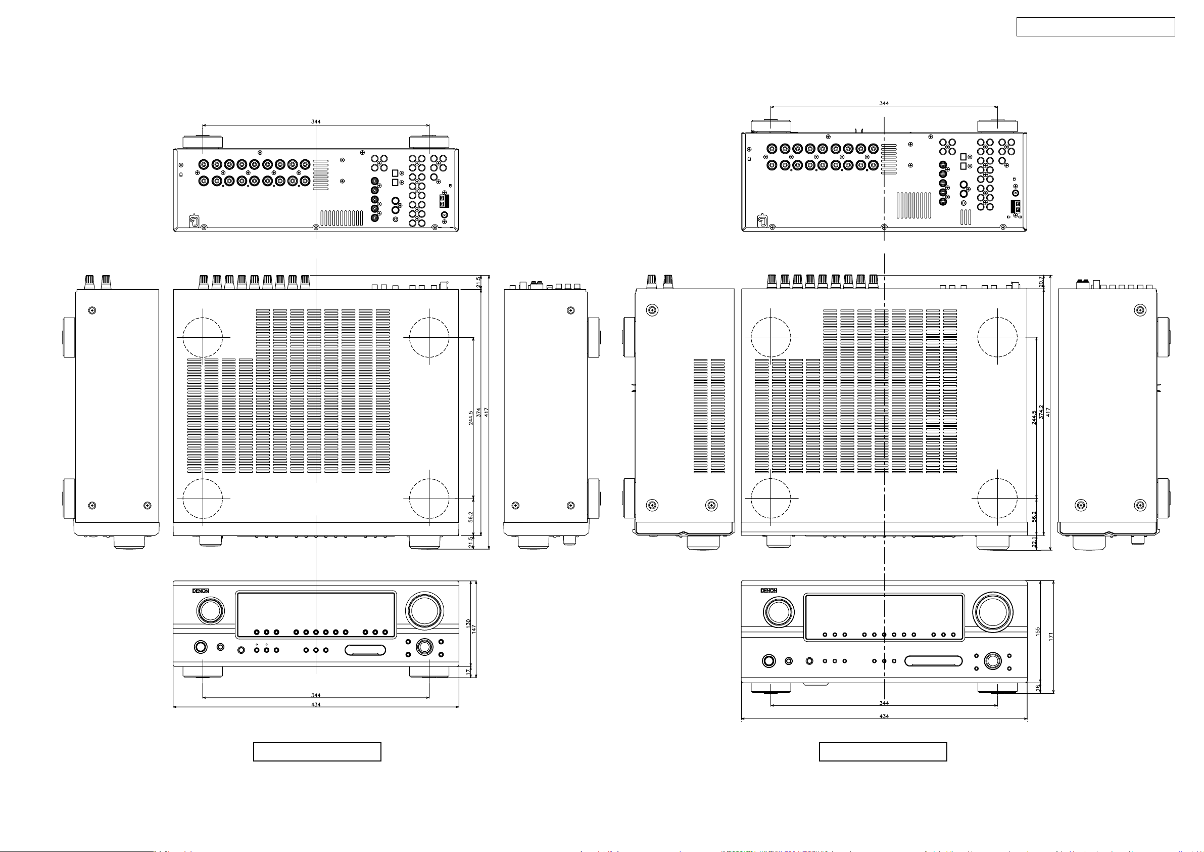
DIMENSION
AVR-1507/1517/1807/1817
AVR-1507/1517 AVR-1807/1817
3
Page 4

AVR-1507/1517/1807/1817
CAUTION IN SERVICING
Initializing AV SURROUND RECEIVER
AV SURROUND RECEIVER initialization should be performed
when the µcom, peripheral parts of µcom , and Digital P.W.B. are
replaced.
1. Switch off the unit.
2. Hold the following SPEAKERS-A button and SPEAKERS-B
button, and switch on the unit.
3. Check that the entire display is flashing with an interval of
about 1 second, and rel ease you r fingers from the 2 buttons
and the microprocessor will be initialized.
Note:・If step 3 does not work, start over from step 1.
・ All user settings will be lost and this factory setting will
be recovered when this initialization mode.
So make sure to memorize your se ttin g for res tori ng
after the initialization.
サービス時の注意事項
AVサラウンドレシーバーの初期化について
マイコンやマイコン周辺部品、Digital 基板等を交換した場合
は、AV サラウンドレシーバーの初期化を行って下さい。
1. オン/オフボタンを OFF にします。
2. SPEAKERS-A ボタンと SPEAKERS-B ボタンを同時に押しな
がら、オン/オフボタンを押して ON にします。
3. ディスプレイ表示が約 1秒間隔で点滅するのを確認後、2
つのボタンから指を離します。
*マイコンが初期化されます。
注意 :・上記 3 の状態にならない場合は、もう一度操作 1 か
らやり直してください。
・初期化を行うとお客様が設定した内容が工場出荷状
態に戻りますので、あらかじめ設定内容を控えてお
き初期化後再設定してください。
4
Page 5
AVR-1507/1517/1807/1817
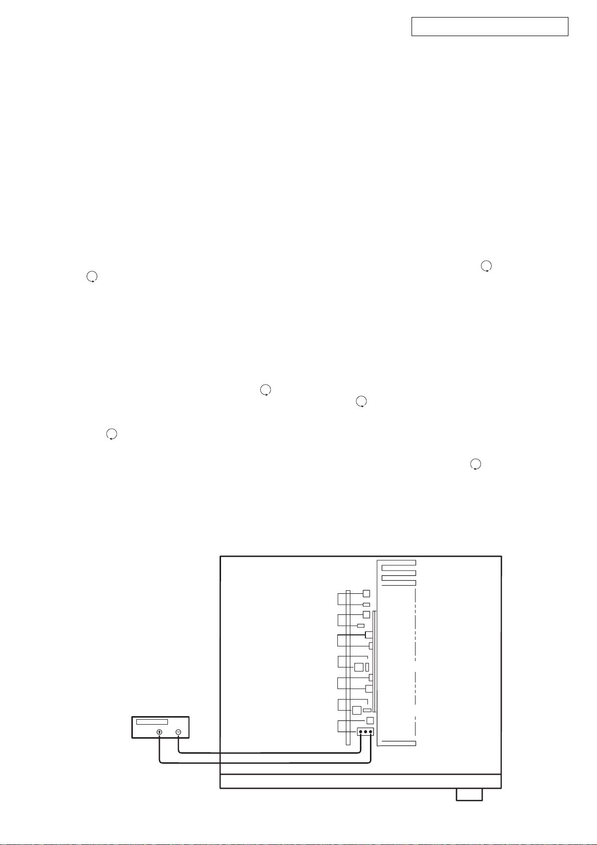
ADJUSTMENT
Audio Section
Idling Current
Required me asurement equipment: DC Voltmeter
1. Preparation
(1) Avoid direct blow from an air conditioner or an electric
fan, and adjust the unit at normal room temperature 15 °C
~ 30 °C (59 °F ~ 86 °F).
(2) Presetting
• PO WER (Power source switch) OFF
• SPEAKER (Speaker terminal) No load
(Do not connect speaker, dummy resistor, etc.)
2. Adjustment
(1) Remove top cover and set VR101, VR102, VR103,
VR104, VR105, on Amp. Unit, VR107SBL,1 07SBR on
2ch Amp. Unit at fully counterclockwise
( ) position.
(2) Connect DC Voltmeter to test points (FRONT-Lch:
TP104, FRONT-Rch: TP105, C ENTER ch: TP1 03, SU RROUND-Lch: TP101, SURROUND-Rch: TP102, SURROUND-BACK Lch: TP106, SURROUND-BACK Rch:
TP107).
(3) Connect power cord to AC Line, and turn power switch
"ON".
(4) Presetting.
MASTER VOLUME: "---" counterclockwise ( min.)
MODE : 7CH STEREO
FUNCTION : CD
(5) Within 2 minutes after the power on, turn VR101 clock-
wise ( ) to adjust th e T EST POINT voltag e to 1 .0 mV
± 0.5 mV DC.
(6) After 10 minutes from the preset above, turn VR101 to
set the voltage to 1.0 mV ± 0.5 mV DC.
(7) Adjust the Variable Resistors of other channels in the
same way.
調整
オーディオセクション
アイドリング電流の調整
調整に必要な測定器 : DCVoltmeter
1. 準備
(1) セットをクーラ、扇風機のそばなど風通しの良い場所
を避け、通常の使用状態に置きます。セットの周囲温
度は 15〜30 ℃、湿度は常湿とします。
(2) プリセット
・電源スイッチ OFF
・スピーカ端子 無負荷
( スピーカ・ダミー抵抗器などを接続しない。)
2. 調整
(1) 上カバーをはずし、パワーアンプ基板の VR101,VR102,
VR103,VR104,VR105 及び 2ch アンプ基板の
VR107SBL,107SBR を反時計方向 ( )に回し切った状
態にセットします。
(2) テストポイント (FRONT-Lch:TP104,FRONT-Rch:
TP105,CENTERch:TP103,SURROUND-Lch:TP101,
SURROUND-Rch:TP102,SURROUND-BACKLch:TP106,
SURROUND-BACKRch:TP107) に DCVoltmeterを接続
します。
(3) 電源コードをラインに接続し、電源スイッチを "ON"に
します。
(4) ON後、次のようにセットします。
・MASTERVOLUME(音量調節つまみ)→反時計方向
( )に回す、最小の状態にする。
・SPEAKER(スピーカ端子)→無負荷(スピーカ、
ダミー抵抗器などを接続しない。)
MODE:7CHSTEREO
FUNCTION:CD
(5) 2分以内に VR101を時計方向 ( ) に回しテストポイ
ントの電圧を次のように調整します。
1.0mV ±0.5mVDC
(6) 予備調整から 10分後 VR101を回し、次のように電圧を
設定します。
1.0mV± 0.5mVDC
(7) 同じ方法で各チャネルの可変抵抗を調整します。
DC Voltmeter
F Lch
S Lch
S Back Rch
C ch
S Back Lch
S Rch
F Rch
5
VR104
TP104
VR101
TP101
VR107
TP107
VR103,TP103
TP106
VR106
VR102,TP102
VR105
TP105
Page 6
BLOCK DIAGRAM
Front Bi-Amp
(AVR-1807/1817 only)
AVR-1507/1517/1807/1817
6
Page 7
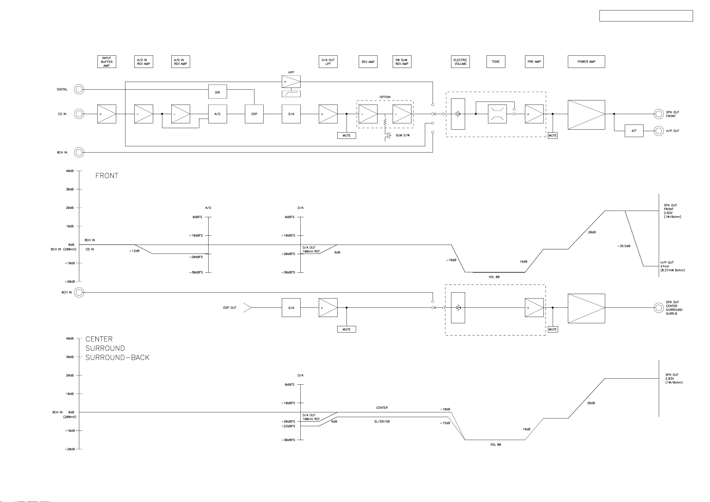
LEVEL DIAGRAMS (1/2)
AVR-1507/1517/1807/1817
NJW1197
NJW1197
7
Page 8
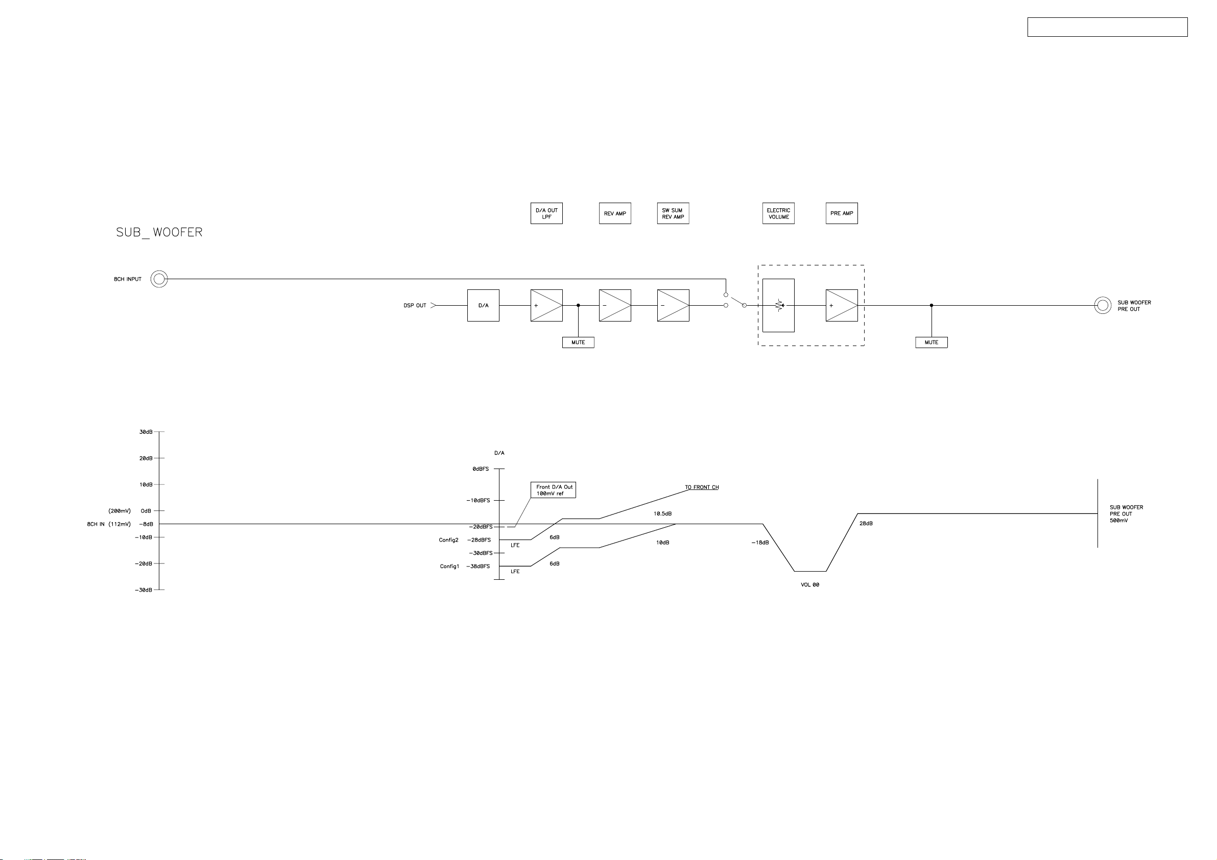
LEVEL DIAGRAMS (2/2)
AVR-1507/1517/1807/1817
NJW1197
8
Page 9
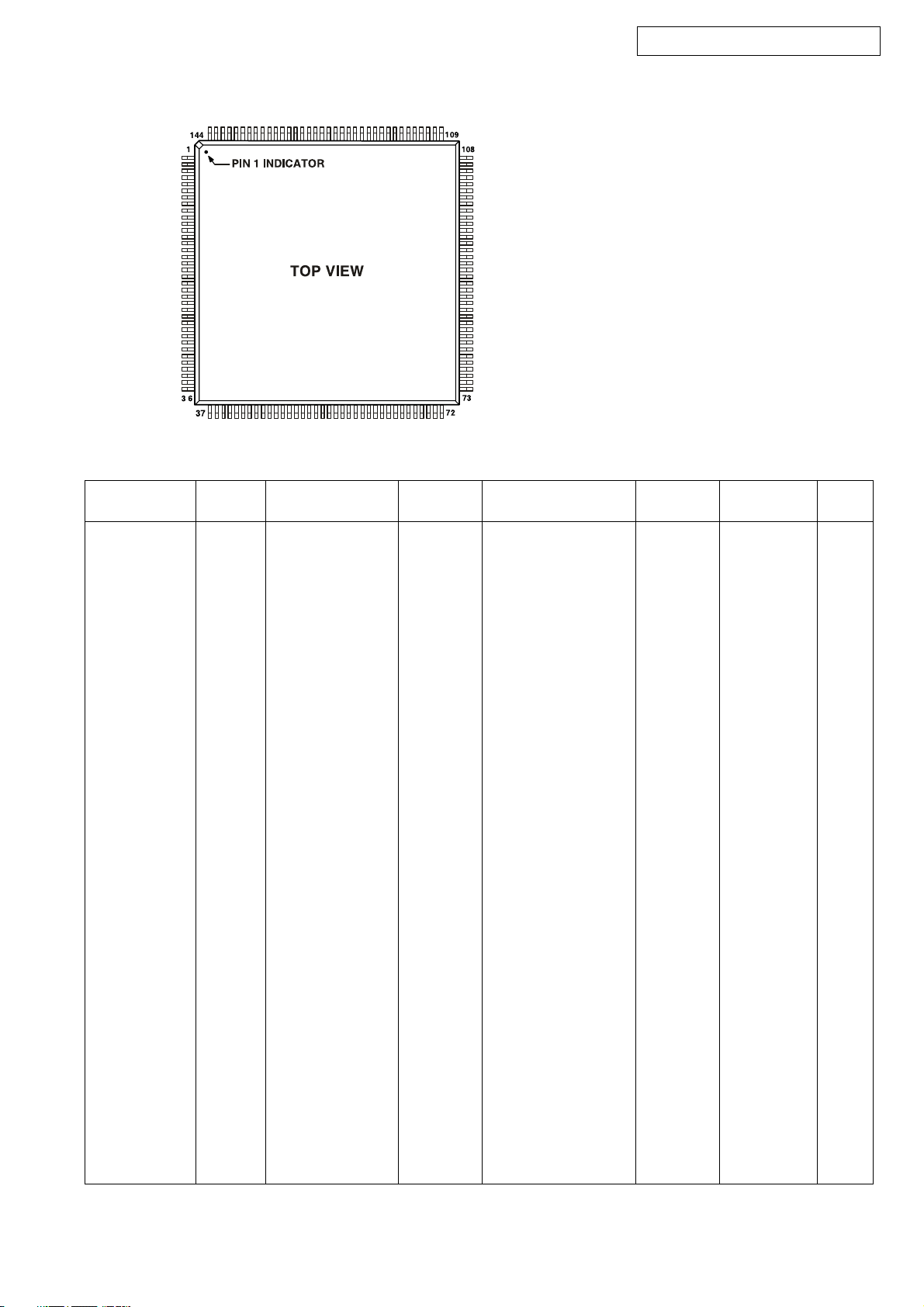
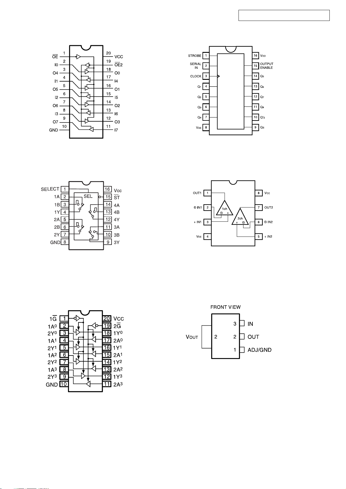
SEMICONDUCTORS
Only major semiconductors are shown, general semiconductors etc. are omitted to list.
主な半導体を記載しています。汎用の半導体は記載を省略しています。
1. IC’s
M30622MEP (IC201)
AVR-1507/1517/1807/1817
9
Page 10
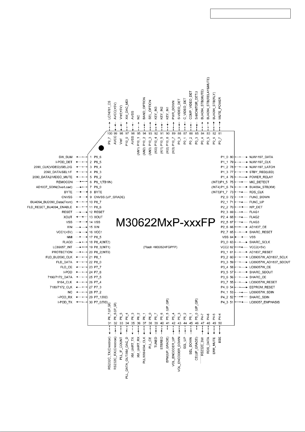
M30622MEP Terminal Function
Pin No. Pin Name I/O/T Pin Function
1 P9_6 O SW_SUM
2 P9_5 O I-POD DET
3 P9_4 O BU209CLK(VIDEO)/SEL2/G
4 P9_3 O BU2090Data/SEL1/F
5 P9_2 O BU2090DATA2/VIDEO_MUTE
6 P9_1(TB1IN) I REMOCON
7 P9_0 I AD1837_SDIN(OverLoad)
8 BYTE I BYTE
9 CNVSS(UP_GRADE) I CNVSS
10 P8_7 O BU4094_BU2090_Data(Front)
11 P8_6 O FLD_RESET_BU4094_ENABLE
12 RESET I RESET
13 XOUT O XOUT
14 VSS I VSS
15 XIN I XIN
16 VCC1 I VCC1(+5V)
17 P8_5 I NMI
18 P8_4(INT2) I FLAG0
19 P8_3(INT1) I LC89057_INT
20 P8_2(INT0) I PROTECTION
21 P8_1 O FLD_BU2090_CLK
22 P8_0 O FLD_DATA
23 P7_7 O FLD_CE
24 P7_6 O I-POD ??PIN
25 P7_5 O 7180/7172_DATA
26 P7_4 O TC9273/9164_CLK
27 P7_3 O 7180/7172_CLK
28 P7_2 O NC
29 P7_1(RXD) I I-POD RX
30 P7_0(TXD) O I-POD TX
31 P6_7(UP_GRADE) O RS232C_TX(Crestron)
32 P6_6(UP_GRADE) I RS232C_RX(Crestron)
33 P6_5 I PLL_IF_COUNT
34 P6_4 O PLL_DATA OUT/XM_DAC_DATA
35 P6_3 O XM_UART_TX
36 P6_2 I XM_UART_RX
37 P6_1 O PLL_CLK/XM_DAC_CLK/BU4094_CLK
38 P6_0 O PLL_CE
39 P5_7 I TUNED
40 P5_6 I STEREO
41 P5_5(UP_GRADE)
42 P5_4 I VOL_ENCODER_UP
43 P5_3 I VOL_ENCODER_DOWN
44 P5_2 I SEL_UP
45 P5_1 I SEL_DOWN
46 P5_0(UP_GRADE)
47 P4-7 O RS232C_SW
48 P4-6 I RDS_DATA
49 P4-5 O ERR_MUTE
50 P4-4 O BSE
51 P4_3 I LC89057_EMPHASIS
52 P4_2 I SHARC_SDIN
53 P4_1 I LC89057W_SDIN
54 P4_0 O EEPROM_RESET
55 P3_7 O LC89057W_RESET
AVR-1507/1517/1807/1817
10
Page 11
Pin No. Pin Name I/O/T Pin Function
56 P3_6 O SHARC_CE
57 P3_5 O SHARC_SDOUT
58 P3_4 O LC89057W_CE
59 P3_3 O LC89057W_AD1837_SDOUT
60 P3_2 O LC89057W_AD1837_SCLK
61 P3_1 O AD1837_RESET
62 VCC2 I VCC2(+5V)
63 P3_0 O SHARC_SCLK
64 VSS I VSS
65 P2_7 O SHARC_RESET
66 P2_6 O AD1837_CE
67 P2_5 I FLAG3
68 P2_4 I FLAG2
69 P2_3 I FLAG1
70 P2_2 I H/P_DET
71 P2_1 I FUNC_ENCODER_UP
72 P2_0 I FUNC_ENCODER_DOWN
73 (INT5)P1_7 I RDS_CLOCK
74 (INT4)P1_6 O 4094_STB(XM)
75 (INT3)P1_5 I MIC_DETECT
76 P1_4 O POWER_RELAY
77 P1_3 O STBY_RED_LED
78 P1_2 O 1197_LATCH
79 P1_1 O 1197_CLK
80 P1_0 O 1197_DATA
81 P0_7 O MUTE_POWER
82 P0_6 O 4094_STB(RLY)
83 P0_5 O 4094_STB(RLY/MUTE)
84 P0_4 O 4094_STB(MUTE)
85 P0_3 I S-MONITOR_DET
86 P0_2 I COMPONENT_DET
87 P0_1 I COMPOSITE_DET
88 P0_0 I S-VIDEO_DET
89 (KI3)P10_7 I POWER_DOWN
90 (KI2)P10_6 I KEY_IN1
91 (KI1)P10_5 I KEY_IN2
92 (KI0)P10_4 I KEY_IN3
93 (AN3)P10_3 I SET_OPTION
94 (AN2)P10_2 I BAND_OPTION
95 (AN1)P10_1 O NC
96 AVSS I AVSS
97 P10_0 O XM_DAC_MDI
98 Vref I Vref(+5V)
99 AVCC I AVCC(+5V)
100 P9_7 O 74781_CS
AVR-1507/1517/1807/1817
11
Page 12
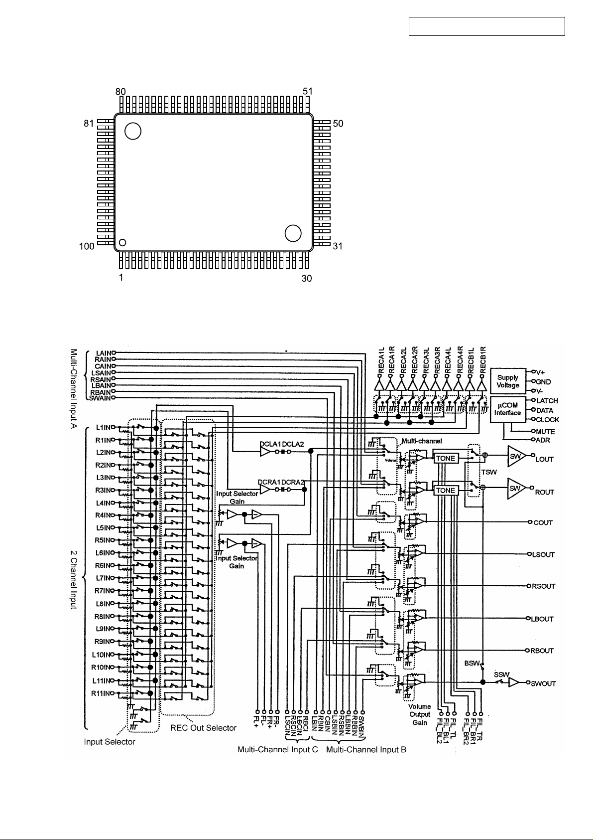
NJW1197 (IC701)
AVR-1507/1517/1807/1817
12
Page 13
AVR-1507/1517/1807/1817
NJW1197 Terminal Function
No. SYMBOL FUNCTION No. SYMBOL FUNCTION
1 ROUT Rch output 51 DCR_IN Multi-channel selector Rch input
2 COUT Cch output 52 DCR_OUT Input selector Rch output
3 LSOUT LSch output 53 GND Ground
4 RSOUT RSch output 54 DCL_IN Multi-channel selector Lch input
5 LBOUT LBch output 55 DCL_OUT Input selector Lch output
6 RBOUT RBch output 56 GND Ground
7 SWOUT SWch output 57 REC_B1R Input selector Rch REC output B1
8 GND Ground 58 RE C_B1L Input selector Lch REC output B1
9 FIL_BL2 Lch Bass filter terminal 2 59 REC_A4R Input selector Rch REC output A4
10 FIL_BL1 Lch Bass filter terminal 1 60 REC_A4L Input selector Lch REC output A4
11 FIL_TL Lch Treble filter terminal 61 REC_A3R Input selector Rch REC output A3
12 TCAP Switching noise rejection capacitor 62 REC_A3L Input selector Lch REC output A3
13 FIL_BR2 Rch Bass filter terminal 2 63 RE C_A2R Input selector Rch REC output A2
14 FIL_BR1 Rch Bass filter terminal 1 64 REC_A2L Input selector Lch REC output A2
15 FIL_TR Rch Treble filter terminal 65 REC_A1R Input selector Rch REC output A1
16 V+ + Power supply voltage input 66 REC_A1L Input selector Lch REC output A1
17 ADR Chip address select input 67 VDDOUT Internal Digital +Power Supply Output
18 V- - Power supply voltage input 68 DATA Control data signal input
19 L1IN Input selector Lch input 1 69 CLOCK Clock signal input
20 DCCAP_SW Switching noise rejection capacitor 70 LATCH Latch signal input
21 R1IN Input selector Rch input 1 71 MUTE External Mute control
22 DCCAP_RB Switching noise rejection capacitor 72 FL+ Input selector gain control Lch no-inverted output
23 L2IN Input selector Lch input 2 73 FL- Input selector gain control Lch inverted output
24 DCCAP_LB Switching noise rejection capacitor 74 FR+ Input selector gain control Rch no-inverted output
25 R2IN Input selector Rch input 2 75 FR- Input selector gain control Rch inverted output
26 DCCAP_RS Switching noise rejection capacitor 76 GND Ground
27 L3IN Input selector Lch input 3 77 LSCIN Multi-channel LSch input C
28 DCCAP_LS Switching noise rejection capacitor 78 RSCIN Multi-channel RSch input C
29 R3IN Input selector Rch input 3 79 LBCIN Multi-channel LBch input C
30 DCCAP_C Switching noise rejection capacitor 80 RBCIN Multi-channel RBch input C
31 L4IN Input selector Lch input 4 81 GND Ground
32 DCCAP_R Switching noise rejection capacitor 82 LAIN Multi-channel Lch input A
33 R4IN Input selector Rch input 4 83 RAIN Multi-channel Rch input A
34 DCCAP_L Switching noise rejection capacitor 84 CAIN Multi-channel Cch input A
35 L5IN Input selector Lch input 5 85 LSAIN Multi-channel LSch input A
36 GND Ground 86 RSAIN Multi-channel RSch input A
37 R5IN Input selector Rch input 5 87 LBAIN Multi-channel LBch input A
38 GND Ground 88 RBAIN Multi-channel RBch input A
39 L6IN Input selector Lch input 6 89 SWAIN Multi-channel SWch input A
40 L9IN Input selector Lch input 9 90 GND Ground
41 R6IN Input selector Rch input 6 91 LBIN Multi-channel Lch input B
42 R9IN Input selector Rch input 9 92 RBIN Multi-channel Rch input B
43 L7IN Input selector Lch input 7 93 CBIN Multi-channel Cch input B
44 L10IN Input selector Lch input 10 94 LSBIN Multi-channel LSch input B
45 R7IN Input selector Rch input 7 95 RSBIN Multi-channel RSch input B
46 R10IN Input selector Rch input 10 96 LBBIN Multi-channel LBch input B
47 L8IN Input selector Lch input 8 97 RBBIN Multi-channel RBch input B
48 L11IN Input selector Lch input 1 1 98 SWBIN Multi-channel SWch input B
49 R8IN Input selector Rch input 8 99 GND Ground
50 R11IN Input selector Rch input 11 100 LOUT Lch output
13
Page 14
ADSP21266SKSTZ-1B (IC804)
ADSP21266SKSTZ-1B Terminal Function
AVR-1507/1517/1807/1817
LQ FP
Pin Name
V
DD INT
Pin # Pin Name
1V
DD INT
CLKCFG0 2 GN D 38 GND 74 V
CLKCFG1 3 RD 39 V
BOOTCFG0 4 ALE 40 GND 76
LQ FP
Pin # Pin Name
37 V
DD EXT
DD INT
LQ FP
Pin # Pin Name
LQ FP
Pin #
73 GND 109
DD IN T
110
75 GND 111
V
DD IN T
112
BOO TCFG1 5 AD 15 41 DAI_P10 (SD2 B) 77 GND 113
GN D 6 AD 14 42 DDAI_P11 (SD3A) 78 V
V
DD EXT
7 AD 13 43 DAI_P12 (SD3 B) 79 GND 115
GN D 8 GN D 44 AI_P13 (SCLK23) 80 V
V
DD INT
9V
DD EXT
45 DAI_P14 (SFS23) 81 GND 117
GN D 10 AD 12 46 DAI_P15 (SD4 A) 82 V
V
DD INT
11 V
DD INT
47 V
DD INT
83 GND 119
GN D 12 GN D 48 GND 84 V
V
DD INT
13 AD 11 49 GND 85 RESET 121
DD IN T
DD EXT
DD IN T
DD IN T
114
116
118
120
GN D 14 AD 10 50 DAI_P16 (SD4 B) 86 SPIDS 122
FLA G0 15 AD 9 51 D A I_P17 (SD5 A) 87 GND 123
FLA G1 16 AD 8 52 DAI_P18 (SD5B) 88 V
DD IN T
124
AD 7 17 DAI_P1 (SD0A) 53 DAI_P19 (SCLK45) 89 SPIC LK 125
GN D 18
V
DD INT
19 GN D 55 91 M OSI 127
V
DD INT
GN D 20 D AI_P2 (SD0B) 56
V
DD EXT
21 DAI_P3 (SC L K0) 57 V
GN D 22 GN D 58 DAI_P20 (SFS45) 94 V
V
DD INT
AD 6 24 V
23 V
DD EXT
DD INT
54 V
DD INT
90 MISO 126
GND
GND
DD EXT
92 GND 128
93 V
59 GND 95 A
60 V
DD INT
96 A
DD IN T
DD EXT
VDD
VSS
129
130
131
132
AD 5 25 GN D 61 FLA G2 97 GND 133
AD 4 26 DAI_P4 (SFS0) 62 FLA G3 98 CLK OUT 134
V
DD INT
27 DAI_P5 (SD1A) 63 V
DD INT
99 EMU 135
GN D 28 D AI_P6 (SD1B) 64 GND 100 TDO 136
AD 3 29 DAI_P7 (SCL K1) 65 V
AD 2 30 V
V
DD EXT
31 GN D 67 V
GN D 32 V
DD INT
DD INT
66 GND 102 TRST 138
68 GND 104 TMS 140
AD 1 33 GN D 69
DD INT
DD INT
V
DD INT
101 TDI 137
103 TCK 139
105 GND 141
AD 0 34 DAI_P8 (SFS1) 70 GND 106 CLKIN 142
WR 35 D A I_P9 (SD2A) 71 V
V
DD INT
36 V
DD INT
72 V
DD INT
DD INT
107 XT AL 143
108 V
DD EXT
144
14
Page 15
LC89057W (IC807)
AVR-1507/1517/1807/1817
15
Page 16
AVR-1507/1517/1807/1817
LC75721E (IC301) BU2090F (IC302)
LA7956 (IC601)
16
Page 17
AD1837AAS (IC808)
AVR-1507/1517/1807/1817
17
Page 18
AVR-1507/1517/1807/1817
MM74LCX244 (IC809-811) BU4094BCF (IC551,552)
74LVX157MTC (IC816) BA4510F (IC815A,816A)
MM74HCT244 (IC812) FAN1117-1.2 (IC824)
RC1117-33 (IC823)
18
Page 19
LH28F800BJE (IC805)
SN74LV573APWR (IC818,819)
AVR-1507/1517/1807/1817
SN74LVC139APWR (IC820)
SN74LV14APWR (IC829)
19
Page 20
MM74HCT00MTCX (IC814,815)
IC63LV1024-10T (IC817)
AVR-1507/1517/1807/1817
20
Page 21
2. FL DISPLAY
HNA-16SM13T (FL301)
AVR-1507/1517/1807/1817
21
Page 22
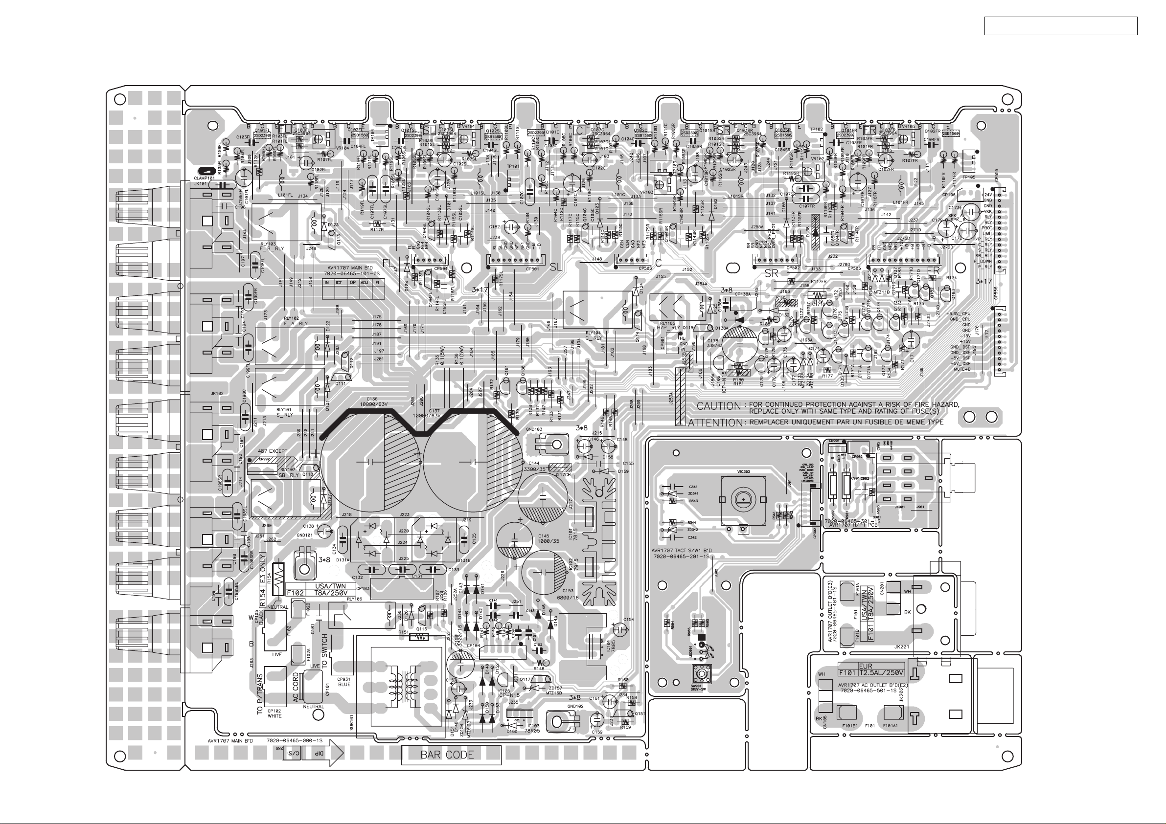
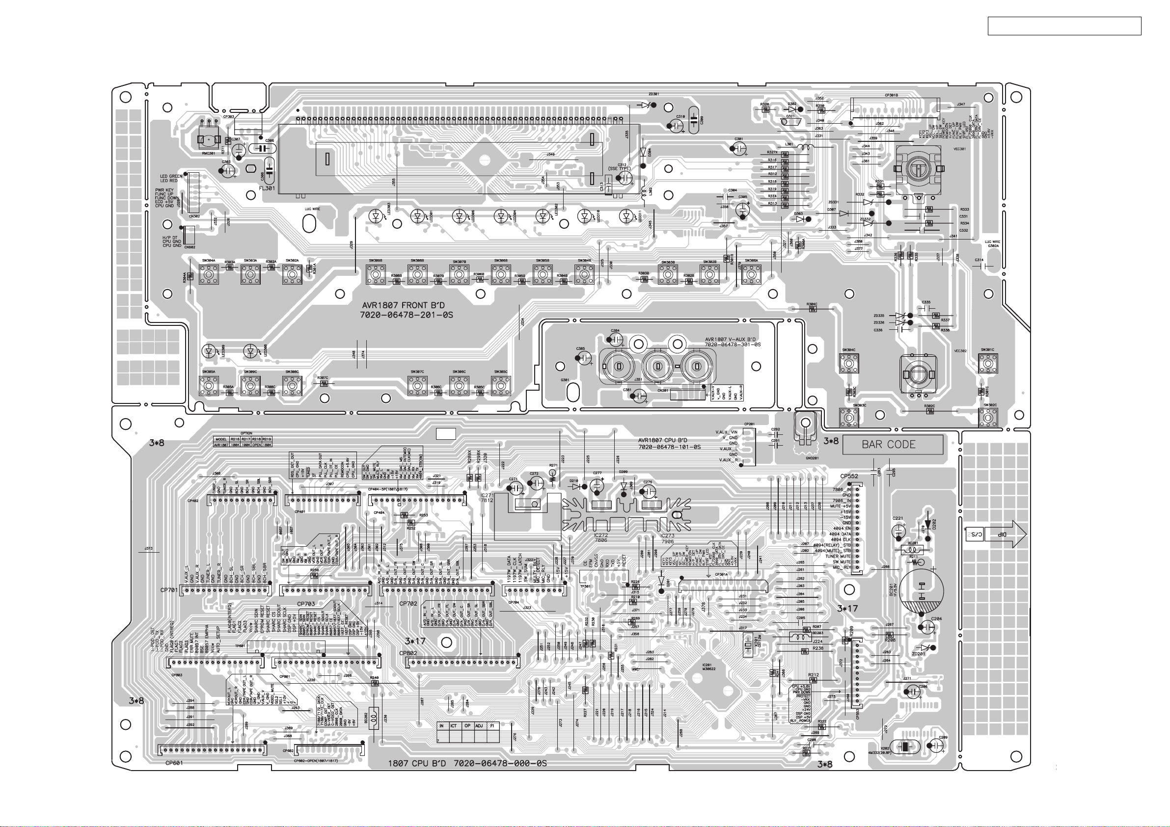
PRINTED WIRING BOARDS
MAIN P.W.B. UNIT (1/2)
AVR-1507/1517/1807/1817
DENON
DENON
DENON
DENON
22
DENON
COMPONENT SIDE
Page 23
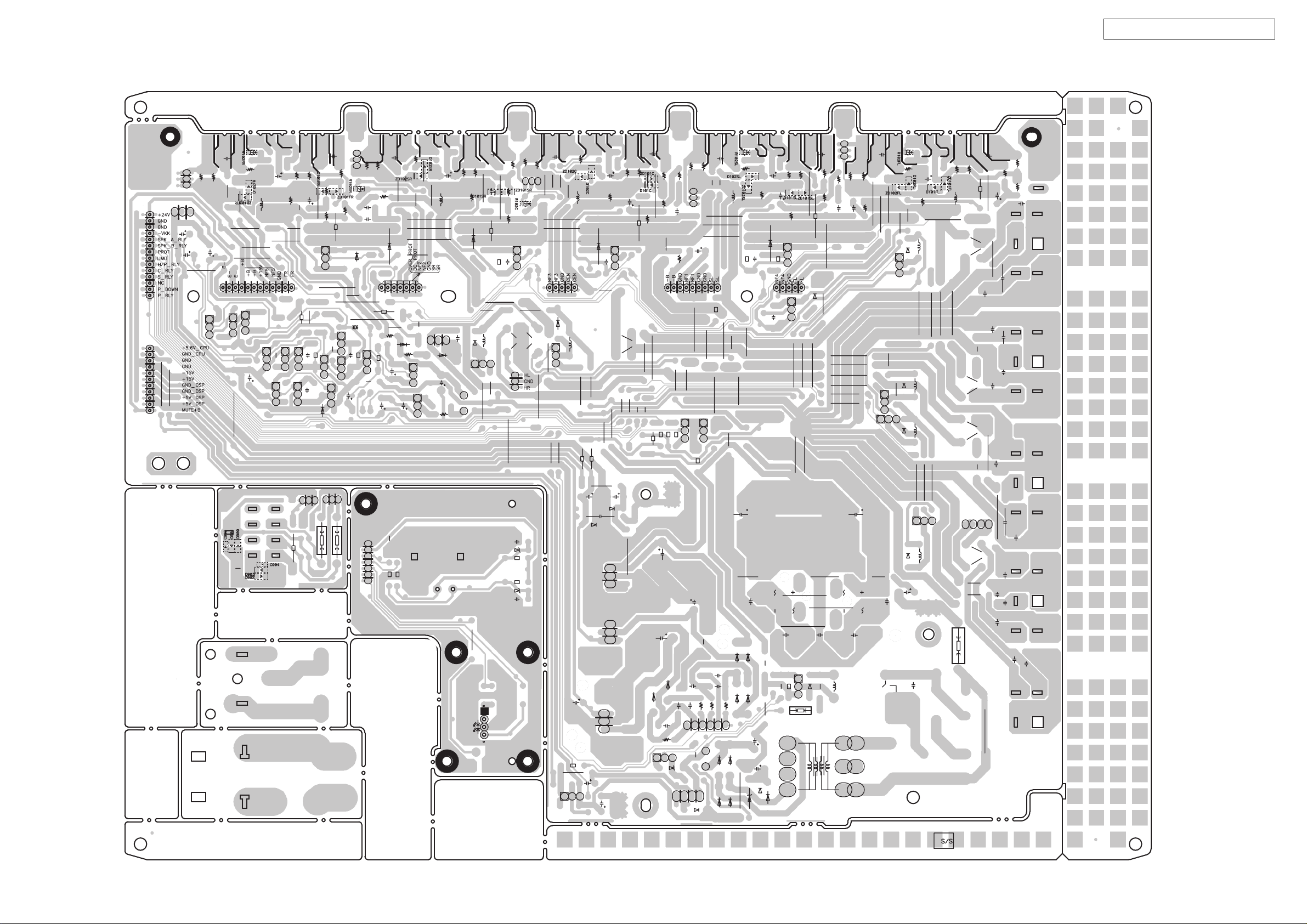
PRINTED WIRING BOARDS
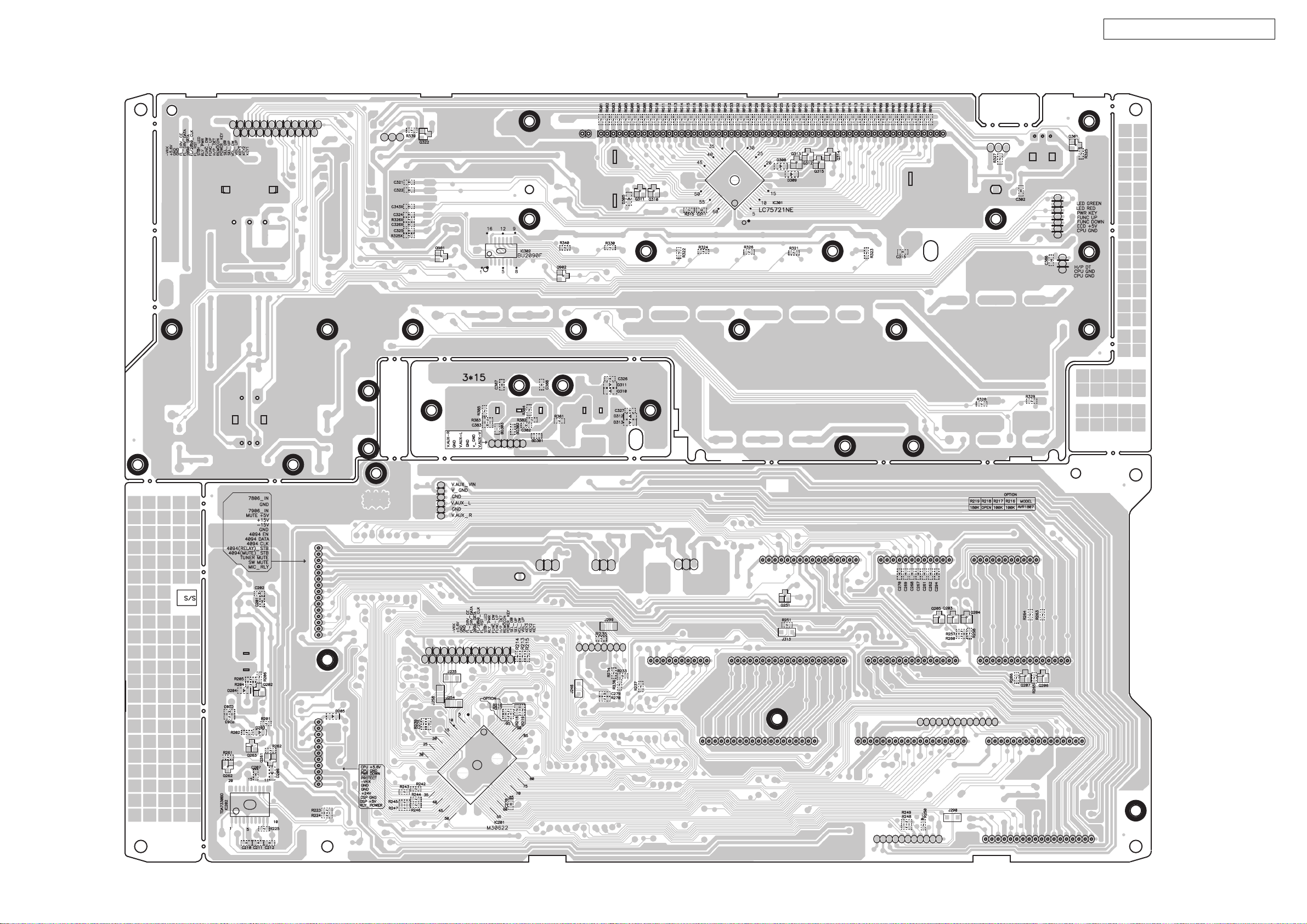
MAIN P.W.B. UNIT (2/2)
AVR-1507/1517/1807/1817
23
FOIL SIDE
Page 24
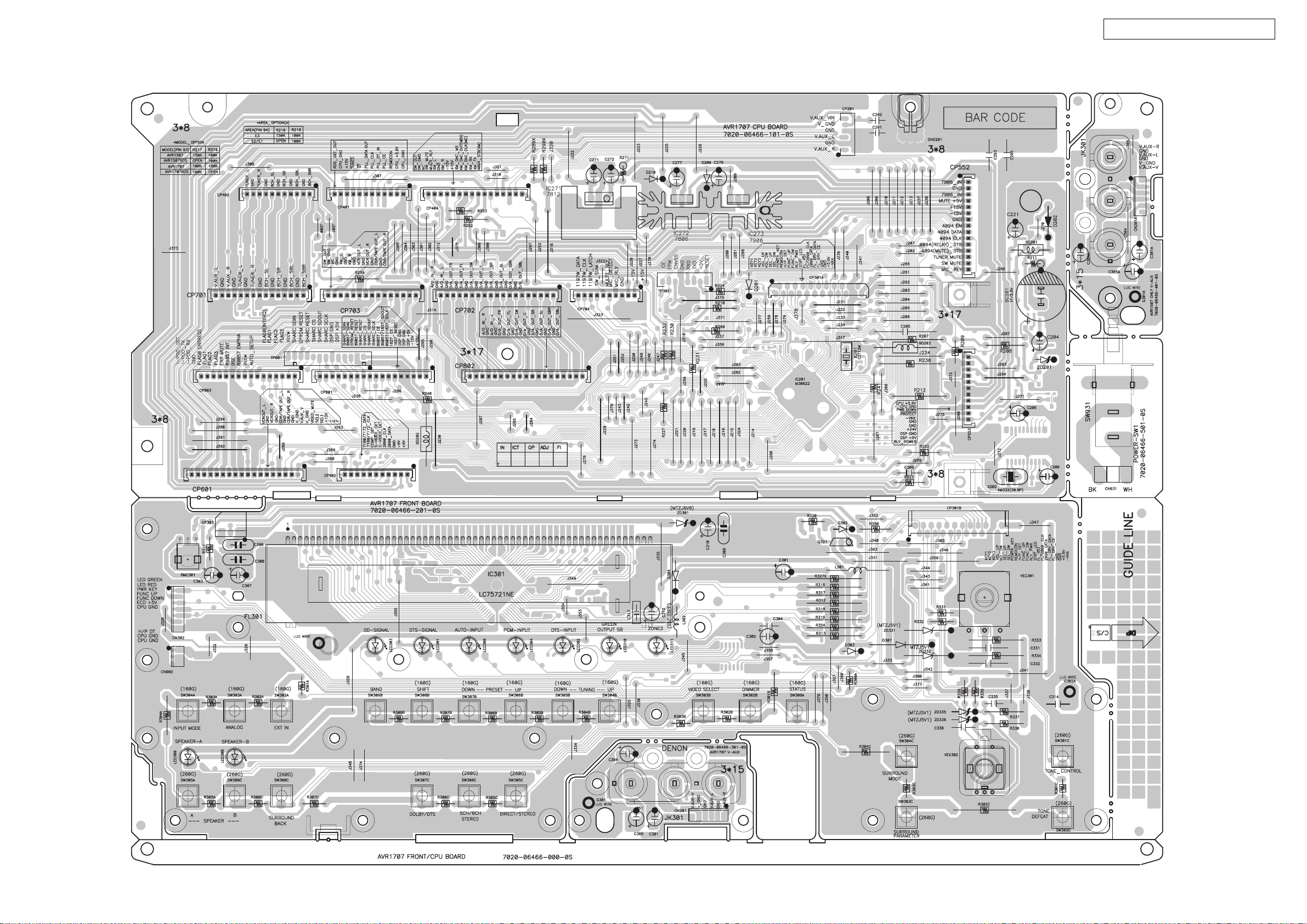
CPU P.W.B. UNIT (1/2) (AVR-1507/1517 MODEL)
AVR-1507/1517/1807/1817
DENON
DENON
DENON
DENON
24
COMPONENT SIDE
Page 25
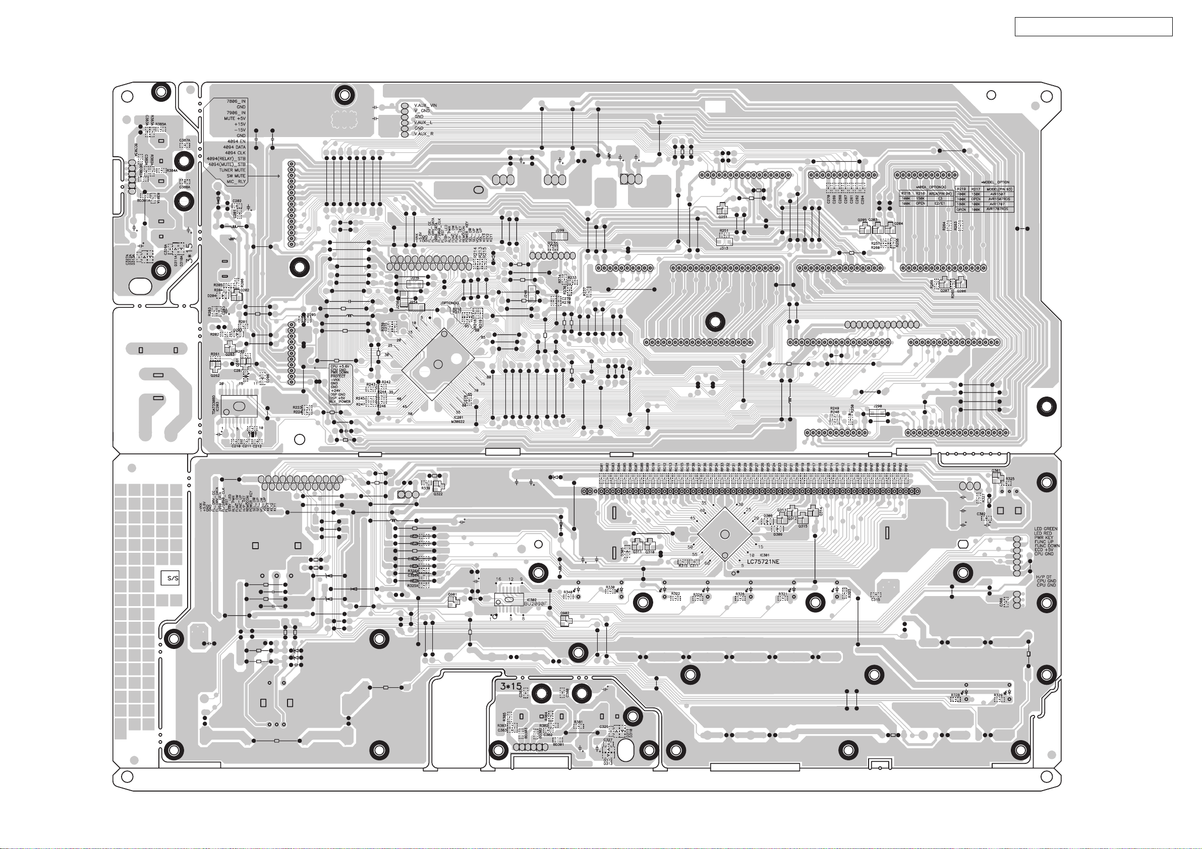
CPU P.W.B. UNIT (2/2) (AVR-1507/1517 MODEL)
AVR-1507/1517/1807/1817
25
FOIL SIDE
Page 26
CPU P.W.B. UNIT (1/2) (AVR-1807/1817 MODEL)
C
AVR-1507/1517/1807/1817
DENON
DENON
DENON
DENON
COMPONENT SIDE
26
Page 27
CPU P.W.B. UNIT (2/2) (AVR-1807/1817 MODEL)
AVR-1507/1517/1807/1817
27
FOIL SIDE
Page 28
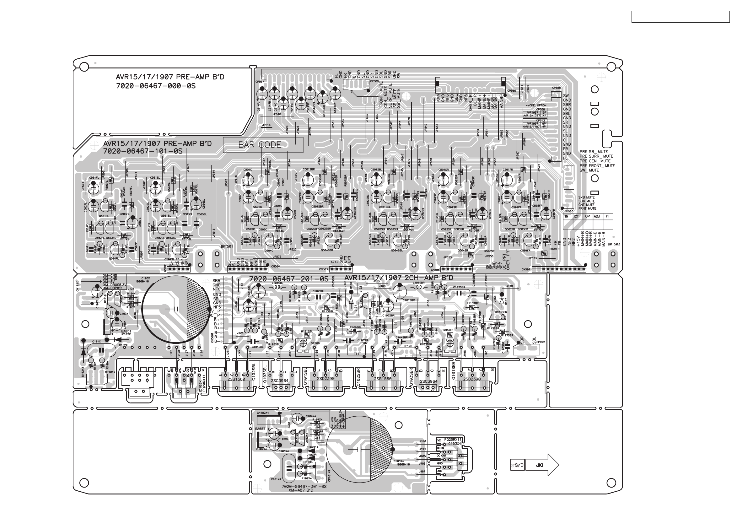
PRE-AMP P.W.B. UNIT (1/2)
DENON
AVR-1507/1517/1807/1817
DENON
DENON
COMPONENT SIDE
28
Page 29

PRE-AMP P.W.B. UNIT (2/2)
AVR-1507/1517/1807/1817
29
FOIL SIDE
Page 30

CNT P.W.B. UNIT
DENON
AVR-1507/1517/1807/1817
COMPONENT SIDE
FOIL SIDE
30
Page 31

INPUT P.W.B. UNIT
AVR-1507/1517/1807/1817
DENON
DENON
COMPONENT SIDE
31
FOIL SIDE
Page 32

8CH-EXT (E2) P.W.B. UNIT
DENON
AVR-1507/1517/1807/1817
COMPONENT SIDE
32
FOIL SIDE
Page 33

DSP1 P.W.B. UNIT (AVR-1807/1817 MODEL)
DENON
AVR-1507/1517/1807/1817
COMPONENT SIDE
33
FOIL SIDE
Page 34

DSP2 P.W.B. UNIT (AVR-1507/1517 MODEL)
DENON
AVR-1507/1517/1807/1817
COMPONENT SIDE
FOIL SIDE
34
Page 35

C- VIDEO1 P.W.B. UNIT (AVR-1807/1817 MODEL)
DENON
AVR-1507/1517/1807/1817
DENON
DENON
DENON
COMPONENT SIDE
35
FOIL SIDE
Page 36

C- VIDEO2 P.W.B. UNIT (AVR-1507/1517 MODEL)
DENON
AVR-1507/1517/1807/1817
COMPONENT SIDE
FOIL SIDE
36
Page 37

AVR-1507/1517/1807/1817
NOTE FOR PARTS LIST
• Part indicated with the mark "nsp" are not always in stock and possibly to
take a long period of time for supplying, or in some case supplying of part
may be refused.
• When ordering of part, clearly indicate "1" and "I" (i) to avoid mis-
supplying.
• Ordering part without stating its part number can not be supplied.
• Part indicated with the mark " ★ " is not illustrated in the exploded view.
• Not including General-purpose Carbon Film Resistor in the P.W.Board
parts list. (Refer to the Schematic Diagram for those parts.)
• Not including General-purpose Carbon Chip Resistor in the P.W.Board
parts list. (Refer to the Schematic Diagram for those parts.)
WARNING:
Parts marked with this symbol
Use ONLY replacement parts recommended by the manufacturer.
ll
l Resistors
ll
Ex.: RN 14K 2E 182 G FR
Type Shape Power Resist- Allowable Others
and per- ance error
formance
RD : Carbon 2B : 1/8W F : ±1% P : Pulse-resistant type
RC : Composition 2E : 1/4W G : ±2% NL : Low noise type
RS : Metal oxide film 2H : 1/2W J : ±5% NB : Non-burning type
RW : Winding 3A : 1W K : ±10% FR : Fuse-resistor
RN : Metal film 3D : 2W M : ±20% F : Lead wire forming
RK : Metal mixture 3F : 3W
] Resistance
1 8 2 ⇒ 1800 ohm = 1.8 kohm
s
s
• Units: ohm
1 R 2 ⇒ 1.2 ohm
s
s
• Units: ohm
Indicates number of zeros after effective number.
2-digit effective number.
1-digit effective number.
2-digit effective number, decimal point indicated by R.
! have critical characteristics.
3H : 5W
部品表について
1.nsp 印の部品は常時在庫していませんので供給に長時間を要すること
があります。
場合によっては、供給をお断りすることがあります。
2.部品を発注する際は特に数字の " 1 " と英字の "I" との区別をはっき
り記入してください。
3.部品番号を表示していない部品は供給できません。
!印の部品は安全上重要な部品です。交換するときは、安全および性
4.
能維持のため必ず指定の部品をご使用ください。
5.★印のついている部品は分解図中には記載していません。
6.汎用カーボン抵抗器は記載していません。定数は回路図を参照願いま
す。
7.汎用カーボンチップ抵抗器は記載していません。定数は回路図を参照
願います。
8.部品表の抵抗器、コンデンサの品名記号の読み方は表を参照してくだ
さい。
RN 14K 2E 182 G FR
RD : 2B : 1/8 W F : ±1% P :
RC : 2E : 1/4 W G : ±2% NL :
RS : 2H : 1/2 W J : ±5% NB :
RW : 3A : 1 W K : ±10% FR :
RN : 3D : 2 W M : ±20% F :
RK : 3F : 3 W
∗
18 2
1R 2
3H : 5 W
1800
Ö
2
1.2
Ö
1
2 R
=1.8k
0
ll
Capacitors
l
ll
Ex.: CE 04W 1H 2R2 M BP
Type Shape Dielectric Capacity Allowable Others
and per- strength error
formance
CE : Aluminum foil 0J : 6.3V F : ±1% HS : High stability type
electrolytic
CA : Aluminum solid 1A : 10V G : ±2% BP : Non-polar type
electrolytic
CS : Tantalum electrolytic 1C : 16V J : ±5% HR : Ripple-resistant type
CQ : Film 1E : 25V K : ±10% DL : For change and discharge
CK : Ceramic 1V : 35V M : ±20% HF : For assuring high
CC :Ceramic 1H : 50V Z : +80% U : UL par t
CP : Oil 2A : 100V –20% C : CSA par t
CM : Mica 2B : 125V P : +100% W : UL-CSA type
CF : Metallized 2C : 160V –0% F : Lead wire forming
CH :Metallized 2D : 200V C : ±0.25pF
] Capacity (electrolyte only)
2 2 2 ⇒ 2200µF
s
s
• Units: µF.
2 R 2 ⇒ 2.2µF
s
s
• Units: µF.
] Capacity (except electrolyte)
2 2 2 ⇒ 2200pF=0.0022µF
s
s
(More than 2) Indicates number of zeros after effective number.
• Units: pF.
2 2 1 ⇒ 220pF
s
s
(0 or 1) Indicates number of zeros after effective number.
• Units: pF.
• When the dielectric strength is indicated in AC, "AC" is included after the dieelectric
strength value.
2E : 250V D : ±0.5pF
2H : 500V = : Others
2J : 630V
Indicates number of zeros after effective number.
2-digit effective number.
1-digit effective number.
2-digit effective number, decimal point indicated by R.
2-digit effective number.
2-digit effective number.
requency
CE 04W 1H 2R2 M BP
CE : 0J : 6.3 V F : ±1% HS :
CA : 1A : 10 V G : ±2% BP :
CS : 1C : 16 V J : ±5% HR :
CQ : 1E : 25 V K : ±10% DL :
CK : 1V : 35 V M : ±20% HF :
CC : 1H : 50 V Z : +80% U : UL
CP : 2A : 100 V −20% C : CSA
CM : 2B : 125 V P : +100% W : UL-CSA
CF : 2C : 160 V − 0% F :
CH : 2D : 200 V C : ±0.25pF
2E : 250 V D : ±0.5pF
2H : 500 V = :
2J : 630 V
∗
22 2
22 2
2200µF
Ö
2
µ
F
2200pF=0.0022µF
Ö
(0 2 )
2
p
F
0
0
2R 2
22 1
Ö
1
2 R
µ
F
Ö
(0 0 1 )
2
p
F
AC
2.2µF
220pF
0
37
Page 38

AVR-1507/1517/1807/1817
PARTS LIST OF P.W.B. UNIT
*本表に記載されている部品は、補修用部品のため製品に使用している部品とは一部、形状、寸法などが異なる場合があります。
* The parts listed below are for maintenance only, might differ from the parts used in the unit in appearances or dimensions.
*"nsp" 印の部品は常時在庫していませんので供給に長時間を要することがあります。場合によっては、供給をお断りする場合があります。
* Part indicated with the mark “nsp” are not always in stock and possibly to take a long period of time for supplying, or in some case supplying of part may be refused.
Note: The symbols in the column "Remarks" indicate the following destinations.
1507 : AVR-1507 Model 1517 : AVR-1517 model
1807 : AVR-1807 Model 1817 : AVR-1817 model
MAIN P.W.B. UNIT ASSY (for AVR-1507/1517 model)
Ref. No. nsp Part No. Part Name Remarks Q'ty New
SEMICONDUCTORS GROUP
IC101 00D 963 0219 408 IC CJ7815 J126781500090S
IC102 00D 963 0219 505 IC CJ7915F J126791500070S
IC103 00D 963 0057 806 IC KIA78R05PI J126780500370S
IC104 00D 963 0219 204 IC CJ7805 J126780500430S
! IC105 00D 960 0195 808 IC ICP-N15 J120001500030S
Q104C 00D 960 0196 506 TR KSC1845F J5021845F0000S
Q104FL 00D 960 0196 506 TR KSC1845F J5021845F0000S
Q104FR 00D 960 0196 506 TR KSC1845F J5021845F0000S
Q104SL 00D 960 0196 506 TR KSC1845F J5021845F0000S
Q104SR 00D 960 0196 506 TR KSC1845F J5021845F0000S
Q111-115 00D 963 0121 208 TR KRC107M J6020107M0010S
Q116 00D 960 0196 409 TR 2SC1740SR J5021740S0010S
Q117,118 00D 963 0121 208 TR KRC107M J6020107M0010S
Q151 00D 960 0196 409 TR 2SC1740SR J5021740S0010S
Q171 00D 960 0196 700 TR KTC3200BL J5023200B0050S
Q171A 00D 960 0196 302 TR KTA1268BL J5001268B0050S
Q171B 00D 960 0196 302 TR KTA1268BL J5001268B0050S
Q171C 00D 960 0196 302 TR KTA1268BL J5001268B0050S
Q171D 00D 960 0196 302 TR KTA1268BL J5001268B0050S
Q172-177 00D 960 0196 700 TR KTC3200BL J5023200B0050S
Q178 00D 960 0196 302 TR KTA1268BL J5001268B0050S
Q179 00D 960 0189 005 TR KSA916Y J5000916Y0050S
Q180,181 00D 960 0196 302 TR KTA1268BL J5001268B0050S
Q182,183 00D 960 0196 700 TR KTC3200BL J5023200B0050S
D101 00D 963 0020 309 D,SWITCHING 1SS133T K000013300520S
D101C 00D 963 0219 709 D,SWITCHING 1N4148W K005041480020S
D101FL 00D 963 0219 709 D,SWITCHING 1N4148W K005041480020S
D101FR 00D 963 0219 709 D,SWITCHING 1N4148W K005041480020S
D101SL 00D 963 0219 709 D,SWITCHING 1N4148W K005041480020S
D101SR 00D 963 0219 709 D,SWITCHING 1N4148W K005041480020S
D102 00D 963 0020 309 D,SWITCHING 1SS133T K000013300520S
D102C 00D 963 0219 709 D,SWITCHING 1N4148W K005041480020S
D102FL 00D 963 0219 709 D,SWITCHING 1N4148W K005041480020S
D102FR 00D 963 0219 709 D,SWITCHING 1N4148W K005041480020S
D102SL 00D 963 0219 709 D,SWITCHING 1N4148W K005041480020S
D103-105 00D 963 0020 309 D,SWITCHING 1SS133T K000013300520S
D121-127 00D 963 0020 309 D,SWITCHING 1SS133T K000013300520S
D131A 00D 960 0197 107
D131B 00D 960 0197 107
D132 00D 963 0020 309 D,SWITCHING 1SS133T K000013300520S
D135 00D 963 0020 309 D,SWITCHING 1SS133T K000013300520S
D138 00D 963 0058 407 D,SWITCHING IN4007 K000400700520S
D141-146 00D 963 0058 407 D,SWITCHING IN4007 K000400700520S
D149,150 00D 963 0058 407 D,SWITCHING IN4007 K000400700520S
D152,153 00D 963 0058 407 D,SWITCHING IN4007 K000400700520S
D900-903 00D 963 0219 709 D,SWITCHING 1N4148W K005041480020S
ZD101C 00D 963 0279 804 D,ZENER 0.2W 4.3V UDZ S K06604R34P410S
ZD101FL 00D 963 0279 804 D,ZENER 0.2W 4.3V UDZ S K06604R34P410S
D,RECTIFIER BRIDGE KBPC604
D,RECTIFIER BRIDGE KBPC604
K047604000020S
K047604000020S
38
Page 39

AVR-1507/1517/1807/1817
Ref. No. nsp Part No. Part Name Remarks Q'ty New
ZD101FR 00D 963 0279 804 D,ZENER 0.2W 4.3V UDZ S K06604R34P410S
ZD101SL 00D 963 0279 804 D,ZENER 0.2W 4.3V UDZ S K06604R34P410S
ZD101SR 00D 963 0279 804 D,ZENER 0.2W 4.3V UDZ S K06604R34P410S
ZD102C 00D 963 0295 503 D,ZENER 0.2W 3.6V UDZ S K06603R64P400S
ZD102FL 00D 963 0295 503 D,ZENER 0.2W 3.6V UDZ S K06603R64P400S
ZD102FR 00D 963 0295 503 D,ZENER 0.2W 3.6V UDZ S K06603R64P400S
ZD102SL 00D 963 0295 503 D,ZENER 0.2W 3.6V UDZ S K06603R64P400S
ZD102SR 00D 963 0295 503 D,ZENER 0.2W 3.6V UDZ S K06603R64P400S
ZD133,134 00D 963 0046 202 D,ZENER MTZJ18B-0.5W/5MA K06018R044520S
ZD136 00D 963 0058 601 D,ZENER MTZJ12B-0.5W/5MA K06012R044520S
ZD154 00D 960 0095 704 D,ZENER MTZJ6.2B-0.5W/5MA K06006R244520S
ZD157 00D 963 0219 903 D,ZENER MTZJ16B-0.5W/5MA K06016R044520S
ZD341,342 00D 960 0095 500 D,ZENER MTZJ5.1B-0.5W/5MA K06005R144520S
LED901 00D 963 0148 605 LED SML1216W RED/GREEN K500052600030S
RESISTORS GROUP
R104C 00D 963 9006 285 R,FIXED 1WJ-5.6K N113135656220S
R104FL 00D 963 9006 285 R,FIXED 1WJ-5.6K N113135656220S
R104FR 00D 963 9006 285 R,FIXED 1WJ-5.6K N113135656220S
R104SL 00D 963 9006 285 R,FIXED 1WJ-5.6K N113135656220S
R104SR 00D 963 9006 285 R,FIXED 1WJ-5.6K N113135656220S
R105C 00D 963 9006 285 R,FIXED 1WJ-5.6K N113135656220S
R105FL 00D 963 9006 285 R,FIXED 1WJ-5.6K N113135656220S
R105FR 00D 963 9006 285 R,FIXED 1WJ-5.6K N113135656220S
R105SL 00D 963 9006 285 R,FIXED 1WJ-5.6K N113135656220S
R106C 00D 963 0215 907 R,METAL FILM 4.7-J,1W C0604R7065050S
R106FL 00D 963 0215 907 R,METAL FILM 4.7-J,1W C0604R7065050S
R106FR 00D 963 0215 907 R,METAL FILM 4.7-J,1W C0604R7065050S
R106SL 00D 963 0215 907 R,METAL FILM 4.7-J,1W C0604R7065050S
R106SR 00D 963 0215 907 R,METAL FILM 4.7-J,1W C0604R7065050S
R107C 00D 963 0215 907 R,METAL FILM 4.7-J,1W C0604R7065050S
R107FL 00D 963 0215 907 R,METAL FILM 4.7-J,1W C0604R7065050S
R107FR 00D 963 0215 907 R,METAL FILM 4.7-J,1W C0604R7065050S
R107SL 00D 963 0215 907 R,METAL FILM 4.7-J,1W C0604R7065050S
R108C 00D 963 9006 269 R,FIXED 1WJ-0.22 N113135622820S
R108FL 00D 963 9006 269 R,FIXED 1WJ-0.22 N113135622820S
R108FR 00D 963 9006 269 R,FIXED 1WJ-0.22 N113135622820S
R108SL 00D 963 9006 269 R,FIXED 1WJ-0.22 N113135622820S
R108SR 00D 963 9006 269 R,FIXED 1WJ-0.22 N113135622820S
R109C 00D 963 9006 269 R,FIXED 1WJ-0.22 N113135622820S
R109FL 00D 963 9006 269 R,FIXED 1WJ-0.22 N113135622820S
R109FR 00D 963 9006 269 R,FIXED 1WJ-0.22 N113135622820S
R109SL 00D 963 9006 269 R,FIXED 1WJ-0.22 N113135622820S
R118C 00D 963 9006 256 R,FIXED 1WJ-10 N113135610020S
R118FL 00D 963 9006 256 R,FIXED 1WJ-10 N113135610020S
R118FR 00D 963 9006 256 R,FIXED 1WJ-10 N113135610020S
R118SL 00D 963 9006 256 R,FIXED 1WJ-10 N113135610020S
R118SR 00D 963 9006 256 R,FIXED 1WJ-10 N113135610020S
R119C 00D 963 9006 256 R,FIXED 1WJ-10 N113135610020S
R119FL 00D 963 9006 256 R,FIXED 1WJ-10 N113135610020S
R119FR 00D 963 9006 256 R,FIXED 1WJ-10 N113135610020S
R119SL 00D 963 9006 256 R,FIXED 1WJ-10 N113135610020S
R135,136 00D 963 0144 502 R,CEMENT 0.1-J 5W C141R10069000S
R141,142 00D 963 0216 003 R,METAL FILM 0.22-J,1W C060R22065050S
R148,149 00D 963 0216 003 R,METAL FILM 0.22-J,1W C060R22065050S
R151 00D 963 0232 809 R,METAL FILM 10-J,1/4W C060010063520S
R179 00D 963 0232 906 R,METAL FILM 47K-F,1/4W C060047343530S
R185 00D 963 9005 655 R,METAL FILM 22-J,1/4W C060022063050S
R901,902 00D 960 9009 270 R,METAL FILM 470-J,2W C060047166520S
VR101-105 00D 960 0091 601 VR,SEMI CERMET 1KB-6.4H3P C544102015130S
39
Page 40

AVR-1507/1517/1807/1817
Ref. No. nsp Part No. Part Name Remarks Q'ty New
CAPACITORS GROUP
C101C 00D 963 0234 506
C101FL 00D 963 0234 506
C101FR 00D 963 0234 506
C101SL 00D 963 0234 506
C101SR 00D 963 0234 506
C102C 00D 963 0234 205 C,ELECT 10UF-M/50V D040100087070S
C102FL 00D 963 0234 205 C,ELECT 10UF-M/50V D040100087070S
C102FR 00D 963 0234 205 C,ELECT 10UF-M/50V D040100087070S
C102SL 00D 963 0234 205 C,ELECT 10UF-M/50V D040100087070S
C102SR 00D 963 0234 205 C,ELECT 10UF-M/50V D040100087070S
C103C 00D 963 9003 084 C,CERAMIC100PF-K/500V D00410106D050S
C103FL 00D 963 9003 084 C,CERAMIC100PF-K/500V D00410106D050S
C103FR 00D 963 9003 084 C,CERAMIC100PF-K/500V D00410106D050S
C103SL 00D 963 9003 084 C,CERAMIC100PF-K/500V D00410106D050S
C103SR 00D 963 9003 084 C,CERAMIC100PF-K/500V D00410106D050S
C104C 00D 963 9003 084 C,CERAMIC100PF-K/500V D00410106D050S
C104FL 00D 963 9003 084 C,CERAMIC100PF-K/500V D00410106D050S
C104FR 00D 963 9003 084 C,CERAMIC100PF-K/500V D00410106D050S
C104SL 00D 963 9003 084 C,CERAMIC100PF-K/500V D00410106D050S
C105C 00D 960 9003 108 C,CERAMIC 0.022UF-Z/25V D005223594520S
C105FL 00D 960 9003 108 C,CERAMIC 0.022UF-Z/25V D005223594520S
C105FR 00D 960 9003 108 C,CERAMIC 0.022UF-Z/25V D005223594520S
C105SL 00D 960 9003 108 C,CERAMIC 0.022UF-Z/25V D005223594520S
C105SR 00D 960 9003 108 C,CERAMIC 0.022UF-Z/25V D005223594520S
C107C 00D 963 9003 097 C,FILM 0.1UF-K/250V D02010407H080S
C107FL 00D 963 9003 097 C,FILM 0.1UF-K/250V D02010407H080S
C107FR 00D 963 9003 097 C,FILM 0.1UF-K/250V D02010407H080S
C107SL 00D 963 9003 097 C,FILM 0.1UF-K/250V D02010407H080S
C107SR 00D 963 9003 097 C,FILM 0.1UF-K/250V D02010407H080S
C131-135 00D 963 9003 097 C,FILM 0.1UF-K/250V D02010407H080S
C136,137 00D 254 6256 002 CE68W1J123M(DL)VNN N211210388110S
C138 00D 963 0293 602 C,ELECT 1UF-M/50V (Pb Free) D040010087150S
C141-143 00D 963 0021 900 C,FILM 0.047UF-J/100V D02047306C060S
C144 00D 963 0217 109 C,ELECT 3300UF-M/35V D040332085010S
C145 00D 963 0311 801 C,ELECT 1000UF-M/35V(SHL) D040102085040S
C146 00D 963 0293 602 C,ELECT 1UF-M/50V (Pb Free) D040010087150S
C148 00D 963 0293 602 C,ELECT 1UF-M/50V (Pb Free) D040010087150S
C150-152 00D 963 0021 900 C,FILM 0.047UF-J/100V D02047306C060S
C153 00D 963 0021 104 C,ELECT 6800UF-M/16V D040682083000S
C154 00D 963 0234 205 C,ELECT 10UF-M/50V D040100087070S
C155 00D 963 0020 202 C,CERAMIC0.1UF-Z/50V D005104597530S
C157 00D 963 0293 602 C,ELECT 1UF-M/50V (Pb Free) D040010087150S
C158 00D 963 0217 002 C,ELECT 3300UF-M/16V D040332083010S
C159 00D 963 0293 602 C,ELECT 1UF-M/50V (Pb Free) D040010087150S
C161 00D 963 0234 205 C,ELECT 10UF-M/50V D040100087070S
C171 00D 963 0293 709 C,ELECT 100UF-M/10V D040101082070S
C171A 00D 963 0020 202 C,CERAMIC 0.1UF-Z/50V D005104597530S
C171B 00D 963 0020 202 C,CERAMIC 0.1UF-Z/50V D005104597530S
C171C 00D 963 0020 202 C,CERAMIC 0.1UF-Z/50V D005104597530S
C171D 00D 963 0020 202 C,CERAMIC 0.1UF-Z/50V D005104597530S
C172,173 00D 963 9005 833 C,ELECT 220UF-M/6.3V D040221081230S
C174 00D 963 0234 506
C175 00D 963 0244 606
C176,177 00D 963 0293 602 C,ELECT 1UF-M/50V (Pb Free) D040010087150S
C178 00D 963 9003 149 C,ELECT 330UF-M/63V D040331088230S
C179 00D 963 9005 833 C,ELECT 220UF-M/6.3V D040221081230S
C181 00D 963 9006 191
C182 00D 963 0234 302 C,ELECT 10UF-M/100V D04010008C050S
C341,342 00D 963 0233 303 C,CERAMIC 0.01UF-M/16V D005103773530S
C901,902 00D 963 0233 206 C,CERAMIC 0.001UF-K/50V D005102177530S
C903,904 nsp 00D 963 9004 698 C,CERAMIC 0.01UF-K/50V D011103777160S
C905 00D 963 0020 202 C,CERAMIC 0.1UF-Z/50V D005104597530S
C,ELECT 47UF-M/50V (Pb Free)
C,ELECT 47UF-M/50V (Pb Free)
C,ELECT 47UF-M/50V (Pb Free)
C,ELECT 47UF-M/50V (Pb Free)
C,ELECT 47UF-M/50V (Pb Free)
C,ELECT 47UF-M/50V (Pb Free)
C,ELECT 0.1UF-M/50V (Pb Free)
C,CERAMICAC(SAFETY)AC13F472MDOA
D040470087070S
D040470087070S
D040470087070S
D040470087070S
D040470087070S
D040470087070S
D040R10087080S
D00847208K070S
40
Page 41

AVR-1507/1517/1807/1817
Ref. No. nsp Part No. Part Name Remarks Q'ty New
OTHERS PARTS GROUP
CLAMP101 nsp 00D 960 0260 005 CLAMP WIRE 4330000120000S
CN901 nsp 00D 963 0184 601 CN,WIRE 260MM/3P L000261030070S
CN992 nsp 00D 963 0235 602 CN,WIRE 270MM/4P L000271040030S
CP101 nsp 00D 963 0262 604 CN.WAFER 2P L108202000220S
CP102 nsp 00D 963 0315 302 CN.WAFER 2P L108353280290S
CP103 nsp 00D 963 0066 208 CN.WAFER 3P L104353280300S
CP104 nsp 00D 960 0128 804 CN.WAFER 6P L102526700600S
CP106 nsp 00D 960 0123 207 CN.WAFER 3P L102526700300S
CP302 nsp 00D 963 0257 800 CN.WAFER 07P L101220070010S
CP501 nsp 00D 963 0206 301 CN.WAFER 5P L101100040510S
CP502 nsp 00D 963 0206 408 CN.WAFER 7P L101100040710S
CP503 nsp 00D 963 0206 301 CN.WAFER 5P L101100040510S
CP504 nsp 00D 963 0206 505 CN.WAFER 9P L101100040910S
CP505 nsp 00D 963 0235 709 CN.WAFER 12P L101100041210S
CP555 nsp 00D 963 0111 108 CN.WAFER 14P L101100041410S
CP556 nsp 00D 963 0087 805 CN.WAFER 11P L101100041110S
CP901,902 nsp 00D 963 0235 806 CN.WAFER 3P L101220030000S
CP931 nsp 00D 963 0315 205 CN.WAFER 2P L108353280280S
! F102 00D 963 0104 801 FUSE T3.15A /250V N751223151110S
F102A - HOLDER,FUSE CLIP G645000050010S
F102B - HOLDER,FUSE CLIP G645000050010S
G901 - CN,WIRE 120MM/1P 8410121010090S
GND101-103 - TERMINAL EARTH 3790040886000S
L101C 00D 963 0049 005 COIL INDUCTOR 0.5UH D330R50000000S
L101FL 00D 963 0049 005 COIL INDUCTOR 0.5UH D330R50000000S
L101FR 00D 963 0049 005 COIL INDUCTOR 0.5UH D330R50000000S
L101SL 00D 963 0049 005 COIL INDUCTOR 0.5UH D330R50000000S
L101SR 00D 963 0049 005 COIL INDUCTOR 0.5UH D330R50000000S
RLY101-104 00D 960 0181 702 RELAY G5PA-28 24V 5A G680240502020S
RLY105 00D 963 0218 506 RELAY BC3-24 24V 2A G680240202040S
RLY106 00D 963 0218 205 RELAY G5PA-1 DC9V 250V/5A G680090102010S
RLY107 00D 960 0181 702 RELAY G5PA-28 24V 5A G680240502020S
SW901 00D 963 0200 103 SW,TACT SKHV10920A G180000270010S
TP101-105 nsp 00D 960 0161 405 CN.WAFER 3P L101530140310S
VEC303 00D 963 0095 208 SW,ENCODER EC16B24SA G121162400040S
- HEAT SINK 2120043538050S
- HEAT SINK 2120044308010S
nsp 00D 963 0247 001 LABEL FUSE (F102) 5527200040030S
! 00D 963 0232 207
nsp 00D 963 0018 007 SCREW, 3*8 B-TYPE ZNY/BH B020030081B10S
00D 963 0158 608 2P TER, SP G611201A0200YS
00D 963 0119 906 8P TER, SP G614801A0200YS
00D 963 0294 708 JACK,D6.5 PHONE G402PJ612AG0YS
- COVER CAPACITOR 4310002640010S
STAND BY TRANS 220V/50,60HZ
8200350150220S
41
Page 42

AVR-1507/1517/1807/1817
MAIN P.W.B. UNIT ASSY (for AVR-1807/1817 model)
Ref. No. nsp Part No. Part Name Remarks ETRO Q'ty New
SEMICONDUCTORS GROUP
IC101 00D 963 0219 408 IC CJ7815 J126781500090S
IC102 00D 963 0219 505 IC CJ7915F J126791500070S
IC103 00D 963 0057 806 IC KIA78R05PI J126780500370S
IC104 00D 963 0219 204 IC CJ7805 J126780500430S
! IC105 00D 960 0195 808 IC ICP-N15 J120001500030S
Q104C 00D 960 0196 506 TR KSC1845F J5021845F0000S
Q104FL 00D 960 0196 506 TR KSC1845F J5021845F0000S
Q104FR 00D 960 0196 506 TR KSC1845F J5021845F0000S
Q104SL 00D 960 0196 506 TR KSC1845F J5021845F0000S
Q104SR 00D 960 0196 506 TR KSC1845F J5021845F0000S
Q111-115 00D 963 0121 208 TR KRC107M J6020107M0010S
Q116 00D 960 0196 409 TR 2SC1740SR J5021740S0010S
Q117,118 00D 963 0121 208 TR KRC107M J6020107M0010S
Q151 00D 960 0196 409 TR 2SC1740SR J5021740S0010S
Q171 00D 960 0196 700 TR KTC3200BL J5023200B0050S
Q171A 00D 960 0196 302 TR KTA1268BL J5001268B0050S
Q171B 00D 960 0196 302 TR KTA1268BL J5001268B0050S
Q171C 00D 960 0196 302 TR KTA1268BL J5001268B0050S
Q171D 00D 960 0196 302 TR KTA1268BL J5001268B0050S
Q172-177 00D 960 0196 700 TR KTC3200BL J5023200B0050S
Q178 00D 960 0196 302 TR KTA1268BL J5001268B0050S
Q179 00D 960 0189 005 TR KSA916Y J5000916Y0050S
Q180,181 00D 960 0196 302 TR KTA1268BL J5001268B0050S
Q182,183 00D 960 0196 700 TR KTC3200BL J5023200B0050S
D101 00D 963 0020 309 D,SWITCHING 1SS133T K000013300520S
D101C 00D 963 0219 709 D,SWITCHING 1N4148W K005041480020S
D101FL 00D 963 0219 709 D,SWITCHING 1N4148W K005041480020S
D101FR 00D 963 0219 709 D,SWITCHING 1N4148W K005041480020S
D101SL 00D 963 0219 709 D,SWITCHING 1N4148W K005041480020S
D101SR 00D 963 0219 709 D,SWITCHING 1N4148W K005041480020S
D102 00D 963 0020 309 D,SWITCHING 1SS133T K000013300520S
D102C 00D 963 0219 709 D,SWITCHING 1N4148W K005041480020S
D102FL 00D 963 0219 709 D,SWITCHING 1N4148W K005041480020S
D102FR 00D 963 0219 709 D,SWITCHING 1N4148W K005041480020S
D102SL 00D 963 0219 709 D,SWITCHING 1N4148W K005041480020S
D102SR 00D 963 0219 709 D,SWITCHING 1N4148W K005041480020S
D103-105 00D 963 0020 309 D,SWITCHING 1SS133T K000013300520S
D121-127 00D 963 0020 309 D,SWITCHING 1SS133T K000013300520S
D131A 00D 960 0197 107
D131B 00D 960 0197 107
D132 00D 963 0020 309 D,SWITCHING 1SS133T K000013300520S
D135 00D 963 0020 309 D,SWITCHING 1SS133T K000013300520S
D138 00D 963 0058 407 D,SWITCHING IN4007 K000400700520S
D141-146 00D 963 0058 407 D,SWITCHING IN4007 K000400700520S
D149,150 00D 963 0058 407 D,SWITCHING IN4007 K000400700520S
D152,153 00D 963 0058 407 D,SWITCHING IN4007 K000400700520S
ZD101C 00D 963 0279 804 D,ZENER 0.2W 4.3V UDZ S K06604R34P410S
ZD101FL 00D 963 0279 804 D,ZENER 0.2W 4.3V UDZ S K06604R34P410S
ZD101FR 00D 963 0279 804 D,ZENER 0.2W 4.3V UDZ S K06604R34P410S
ZD101SL 00D 963 0279 804 D,ZENER 0.2W 4.3V UDZ S K06604R34P410S
ZD101SR 00D 963 0279 804 D,ZENER 0.2W 4.3V UDZ S K06604R34P410S
ZD102C 00D 963 0295 503 D,ZENER 0.2W 3.6V UDZ S K06603R64P400S
ZD102FL 00D 963 0295 503 D,ZENER 0.2W 3.6V UDZ S K06603R64P400S
ZD102FR 00D 963 0295 503 D,ZENER 0.2W 3.6V UDZ S K06603R64P400S
ZD102SL 00D 963 0295 503 D,ZENER 0.2W 3.6V UDZ S K06603R64P400S
ZD102SR 00D 963 0295 503 D,ZENER 0.2W 3.6V UDZ S K06603R64P400S
ZD133,134 00D 963 0046 202 D,ZENER MTZJ18B K06018R044520S
D,RECTIFIER BRIDGE KBPC604
D,RECTIFIER BRIDGE KBPC604
K047604000020S
K047604000020S
42
Page 43

AVR-1507/1517/1807/1817
Ref. No. nsp Part No. Part Name Remarks ETRO Q'ty New
ZD136 00D 963 0058 601 D,ZENER MTZJ12B K06012R044520S
ZD154 00D 960 0095 704 D,ZENER MTZJ6.2B K06006R244520S
ZD157 00D 963 0219 903 D,ZENER MTZJ16B K06016R044520S
RESISTORS GROUP
R104C 00D 963 9006 285 R,FIXED 1WJ-5.6K N113135656220S
R104FL 00D 963 9006 285 R,FIXED 1WJ-5.6K N113135656220S
R104FR 00D 963 9006 285 R,FIXED 1WJ-5.6K N113135656220S
R104SL 00D 963 9006 285 R,FIXED 1WJ-5.6K N113135656220S
R104SR 00D 963 9006 285 R,FIXED 1WJ-5.6K N113135656220S
R105C 00D 963 9006 285 R,FIXED 1WJ-5.6K N113135656220S
R105FL 00D 963 9006 285 R,FIXED 1WJ-5.6K N113135656220S
R105FR 00D 963 9006 285 R,FIXED 1WJ-5.6K N113135656220S
R105SL 00D 963 9006 285 R,FIXED 1WJ-5.6K N113135656220S
R105SR 00D 963 9006 285 R,FIXED 1WJ-5.6K N113135656220S
R106C 00D 963 0215 907 R,METAL FILM 4.7-J,1W C0604R7065050S
R106FL 00D 963 0215 907 R,METAL FILM 4.7-J,1W C0604R7065050S
R106FR 00D 963 0215 907 R,METAL FILM 4.7-J,1W C0604R7065050S
R106SL 00D 963 0215 907 R,METAL FILM 4.7-J,1W C0604R7065050S
R106SR 00D 963 0215 907 R,METAL FILM 4.7-J,1W C0604R7065050S
R107C 00D 963 0215 907 R,METAL FILM 4.7-J,1W C0604R7065050S
R107FL 00D 963 0215 907 R,METAL FILM 4.7-J,1W C0604R7065050S
R107FR 00D 963 0215 907 R,METAL FILM 4.7-J,1W C0604R7065050S
R107SL 00D 963 0215 907 R,METAL FILM 4.7-J,1W C0604R7065050S
R108C 00D 963 9006 269 R,FIXED 1WJ-0.22 N113135622820S
R108FL 00D 963 9006 269 R,FIXED 1WJ-0.22 N113135622820S
R108FR 00D 963 9006 269 R,FIXED 1WJ-0.22 N113135622820S
R108SL 00D 963 9006 269 R,FIXED 1WJ-0.22 N113135622820S
R108SR 00D 963 9006 269 R,FIXED 1WJ-0.22 N113135622820S
R109C 00D 963 9006 269 R,FIXED 1WJ-0.22 N113135622820S
R109FL 00D 963 9006 269 R,FIXED 1WJ-0.22 N113135622820S
R109FR 00D 963 9006 269 R,FIXED 1WJ-0.22 N113135622820S
R109SL 00D 963 9006 269 R,FIXED 1WJ-0.22 N113135622820S
R118C 00D 963 9006 256 R,FIXED 1WJ-10 N113135610020S
R118FL 00D 963 9006 256 R,FIXED 1WJ-10 N113135610020S
R118FR 00D 963 9006 256 R,FIXED 1WJ-10 N113135610020S
R118SL 00D 963 9006 256 R,FIXED 1WJ-10 N113135610020S
R118SR 00D 963 9006 256 R,FIXED 1WJ-10 N113135610020S
R119C 00D 963 9006 256 R,FIXED 1WJ-10 N113135610020S
R119FL 00D 963 9006 256 R,FIXED 1WJ-10 N113135610020S
R119FR 00D 963 9006 256 R,FIXED 1WJ-10 N113135610020S
R119SL 00D 963 9006 256 R,FIXED 1WJ-10 N113135610020S
R135,136 00D 963 0144 502 R,CEMENT 0.1-J 5W C141R10069000S
R141,142 00D 963 0216 003 R,METAL FILM 0.22-J,1W C060R22065050S
R148,149 00D 963 0216 003 R,METAL FILM 0.22-J,1W C060R22065050S
R151 00D 963 0232 809 R,METAL FILM 10-J,1/4W C060010063520S
R179 00D 963 0232 906 R,METAL FILM 47K-F,1/4W C060047343530S
R185 00D 963 9005 655 R,METAL FILM 22-J,1/4W C060022063050S
VR101-105 00D 960 0091 601 VR,SEMI CERMET 1KB-6.4H3P C544102015130S
CAPACITORS GROUP
C101C 00D 963 0234 506
C101FL 00D 963 0234 506
C101FR 00D 963 0234 506
C101SL 00D 963 0234 506
C101SR 00D 963 0234 506
C102C 00D 963 0234 205 C,ELECT 10UF-M/50V D040100087070S
C102FL 00D 963 0234 205 C,ELECT 10UF-M/50V D040100087070S
C102FR 00D 963 0234 205 C,ELECT 10UF-M/50V D040100087070S
C102SL 00D 963 0234 205 C,ELECT 10UF-M/50V D040100087070S
C102SR 00D 963 0234 205 C,ELECT 10UF-M/50V D040100087070S
C,ELECT 47UF-M/50V(Pb Free)
C,ELECT 47UF-M/50V(Pb Free)
C,ELECT 47UF-M/50V(Pb Free)
C,ELECT 47UF-M/50V(Pb Free)
C,ELECT 47UF-M/50V(Pb Free)
D040470087070S
D040470087070S
D040470087070S
D040470087070S
D040470087070S
43
Page 44

AVR-1507/1517/1807/1817
Ref. No. nsp Part No. Part Name Remarks ETRO Q'ty New
C103C 00D 963 9003 084 C,CERAMIC 100PF-K/500V D00410106D050S
C103FL 00D 963 9003 084 C,CERAMIC 100PF-K/500V D00410106D050S
C103FR 00D 963 9003 084 C,CERAMIC 100PF-K/500V D00410106D050S
C103SL 00D 963 9003 084 C,CERAMIC 100PF-K/500V D00410106D050S
C103SR 00D 963 9003 084 C,CERAMIC 100PF-K/500V D00410106D050S
C104C 00D 963 9003 084 C,CERAMIC 100PF-K/500V D00410106D050S
C104FL 00D 963 9003 084 C,CERAMIC 100PF-K/500V D00410106D050S
C104FR 00D 963 9003 084 C,CERAMIC 100PF-K/500V D00410106D050S
C104SL 00D 963 9003 084 C,CERAMIC 100PF-K/500V D00410106D050S
C105C 00D 960 9003 108 C,CERAMIC 0.022UF-Z/25V D005223594520S
C105FL 00D 960 9003 108 C,CERAMIC 0.022UF-Z/25V D005223594520S
C105FR 00D 960 9003 108 C,CERAMIC 0.022UF-Z/25V D005223594520S
C105SL 00D 960 9003 108 C,CERAMIC 0.022UF-Z/25V D005223594520S
C105SR 00D 960 9003 108 C,CERAMIC 0.022UF-Z/25V D005223594520S
C107C 00D 963 9003 097 C,FILM 0.1UF-K/250V D02010407H080S
C107FL 00D 963 9003 097 C,FILM 0.1UF-K/250V D02010407H080S
C107FR 00D 963 9003 097 C,FILM 0.1UF-K/250V D02010407H080S
C107SL 00D 963 9003 097 C,FILM 0.1UF-K/250V D02010407H080S
C107SR 00D 963 9003 097 C,FILM 0.1UF-K/250V D02010407H080S
C131-135 00D 963 9003 097 C,FILM 0.1UF-K/250V D02010407H080S
C136,137 00D 254 6256 002 CE68W1J123M(DL)VNN N211210388110S
C138 00D 963 0293 602 C,ELECT 1UF-M/50V (Pb Free) D040010087150S
C141-143 00D 963 0021 900 C,FILM 0.047UF-J/100V D02047306C060S
C144 00D 963 0217 109 C,ELECT 3300UF-M/35V D040332085010S
C145 00D 963 0311 801 C,ELECT 1000UF-M/35V D040102085040S
C146 00D 963 0293 602 C,ELECT 1UF-M/50V (Pb Free) D040010087150S
C148 00D 963 0293 602 C,ELECT 1UF-M/50V (Pb Free) D040010087150S
C150-152 00D 963 0021 900 C,FILM 0.047UF-J/100V D02047306C060S
C153 00D 963 0021 104 C,ELECT 6800UF-M/16V D040682083000S
C154 00D 963 0234 205 C,ELECT 10UF-M/50V D040100087070S
C155 00D 963 0020 202 C,CERAMIC 0.1UF-Z/50V D005104597530S
C157 00D 963 0293 602 C,ELECT 1UF-M/50V (Pb Free) D040010087150S
C158 00D 963 0217 002 C,ELECT 3300UF-M/16V D040332083010S
C159 00D 963 0293 602 C,ELECT 1UF-M/50V (Pb Free) D040010087150S
C161 00D 963 0234 205 C,ELECT 10UF-M/50V D040100087070S
C171 00D 963 0293 709 C,ELECT 100UF-M/10V D040101082070S
C171A 00D 963 0020 202 C,CERAMIC 0.1UF-Z/50V D005104597530S
C171B 00D 963 0020 202 C,CERAMIC 0.1UF-Z/50V D005104597530S
C171C 00D 963 0020 202 C,CERAMIC 0.1UF-Z/50V D005104597530S
C171D 00D 963 0020 202 C,CERAMIC 0.1UF-Z/50V D005104597530S
C172,173 00D 963 9005 833 C,ELECT 220UF-M/6.3V D040221081230S
C174 00D 963 0234 506
C175 00D 963 0244 606
C176,177 00D 963 0293 602 C,ELECT 1UF-M/50V (Pb Free) D040010087150S
C178 00D 963 9003 149 C,ELECT 330UF-M/63V D040331088230S
C179 00D 963 9005 833 C,ELECT 220UF-M/6.3V D040221081230S
C181 00D 963 9006 191
C182 00D 963 0234 302 C,ELECT 10UF-M/100V D04010008C050S
OTHERS PARTS GROUP
CLAMP101 nsp 00D 960 0260 005 CLAMP WIRE 4330000120000S
CN992 nsp 00D 963 0235 602 CN,WIRE 270MM/4P L000271040030S
CP101 nsp 00D 963 0262 604 CN.WAFER 2P L108202000220S
CP102 nsp 00D 963 0315 302 CN.WAFER 2P L108353280290S
CP103 nsp 00D 963 0066 208 CN.WAFER 3P L104353280300S
CP104 nsp 00D 960 0128 804 CN.WAFER 6P L102526700600S
CP106 nsp 00D 960 0123 207 CN.WAFER 3P L102526700300S
CP501 nsp 00D 963 0206 301 CN.WAFER 5P L101100040510S
CP502 nsp 00D 963 0206 408 CN.WAFER 7P L101100040710S
CP503 nsp 00D 963 0206 301 CN.WAFER 5P L101100040510S
CP504 nsp 00D 963 0206 505 CN.WAFER 9P L101100040910S
C,ELECT 47UF-M/50V(Pb Free)
C,ELECT 0.1UF-M/50V (Pb Free)
C,CERAMIC AC(SAFETY) AC13F472MDOA
D040470087070S
D040R10087080S
D00847208K070S
44
Page 45

AVR-1507/1517/1807/1817
Ref. No. nsp Part No. Part Name Remarks ETRO Q'ty New
CP505 nsp 00D 963 0235 709 CN.WAFER 12P L101100041210S
CP555 nsp 00D 963 0111 108 CN.WAFER 14P L101100041410S
CP556 nsp 00D 963 0087 805 CN.WAFER 11P L101100041110S
CP901 nsp 00D 963 0235 806 CN.WAFER 3P L101220030000S
CP931 nsp 00D 963 0315 205 CN.WAFER 2P L108353280280S
! F102 00D 963 0104 801 FUSE T3.15A /250V N751223151110S
F102A - HOLDER,FUSE CLIP G645000050010S
F102B - HOLDER,FUSE CLIP G645000050010S
GND101-103 - TERMINAL EARTH 3790040886000S
L101C 00D 963 0049 005 COIL INDUCTOR 0.5UH D330R50000000S
L101FL 00D 963 0049 005 COIL INDUCTOR 0.5UH D330R50000000S
L101FR 00D 963 0049 005 COIL INDUCTOR 0.5UH D330R50000000S
L101SL 00D 963 0049 005 COIL INDUCTOR 0.5UH D330R50000000S
L101SR 00D 963 0049 005 COIL INDUCTOR 0.5UH D330R50000000S
RLY101-104 00D 960 0181 702 RELAY G5PA-28 24V 5A G680240502020S
RLY105 00D 963 0218 506 RELAY BC3-24 24V 2A G680240202040S
RLY106 00D 963 0218 205 RELAY G5PA-1 DC9V 250V/5A G680090102010S
RLY107 00D 960 0181 702 RELAY G5PA-28 24V 5A G680240502020S
TP101-105 nsp 00D 960 0161 405 CN.WAFER 3P L101530140310S
- HEAT SINK 2120043538050S
- HEAT SINK 2120044308010S
nsp 00D 963 0247 001 LABEL FUSE (F102) 5527200040030S
! 00D 963 0232 207
nsp 00D 963 0018 007 SCREW, 3*8 B-TYPE ZNY/BH B020030081B10S
00D 963 0158 608 2P TER, SP G611201A0200YS
00D 963 0119 906 8P TER, SP G614801A0200YS
- COVER CAPACITOR 4310002640010S
STAND BY TRANS 220V/50,60HZ
8200350150220S
45
Page 46

AVR-1507/1517/1807/1817
CPU P.W.B. UNIT ASSY (for AVR-1507/1517 model)
Ref. No. nsp Part No. Part Name Remarks Q'ty New
SEMICONDUCTORS GROUP
IC201 00D 262 3651 009 M3062LFGPFP J020306200010S
IC271 00D 963 0252 902 IC CJ7812 J126781200230S
IC301 00D 262 2549 002 LC75721E +C J127757210010S
IC302 00D 963 0074 504 IC BU2090 J044209000010S
Q202 00D 963 0121 509 TR KTC3875S J522038750210S
Q203,204 00D 963 0044 301 TR KTC2875B J5222875B0010S
Q205 00D 963 0120 704 TR KRA102S J520010200210S
Q206,207 00D 963 0044 301 TR KTC2875B J5222875B0010S
Q251 00D 963 0120 704 TR KRA102S J520010200210S
Q263 00D 960 0285 006 TR KRC104S J522104S00210S
Q301 00D 963 0120 704 TR KRA102S J520010200210S
Q310 00D 963 0120 704 TR KRA102S J520010200210S
Q311 00D 963 0120 801 TR KRC102S J522010200210S
Q312 00D 963 0120 704 TR KRA102S J520010200210S
Q313 00D 963 0120 801 TR KRC102S J522010200210S
Q314 00D 963 0120 704 TR KRA102S J520010200210S
Q315 00D 963 0120 801 TR KRC102S J522010200210S
Q321 00D 963 0102 803 TR 2SA933S J5000933S0050S
Q322 00D 960 0111 808 TR KRC107S J5020107S0050S
Q901,902 00D 963 0120 704 TR KRA102S J520010200210S
D201 00D 963 0020 309 D,SWITCHING 1SS133T K000013300520S
D202 00D 963 0058 407 D,SWITCHING IN4007 K000400700520S
D203-205 00D 963 0219 709 D,SWITCHING 1N4148W K005041480020S
D302-304 00D 963 0020 309 D,SWITCHING 1SS133T K000013300520S
D305 00D 963 0219 709 D,SWITCHING 1N4148W K005041480020S
D307 00D 963 0020 309 D,SWITCHING 1SS133T K000013300520S
D308,309 00D 963 0219 709 D,SWITCHING 1N4148W K005041480020S
D310A 00D 963 0219 709 D,SWITCHING 1N4148W K005041480020S
D311A 00D 963 0219 709 D,SWITCHING 1N4148W K005041480020S
D312A 00D 963 0219 709 D,SWITCHING 1N4148W K005041480020S
D313A 00D 963 0219 709 D,SWITCHING 1N4148W K005041480020S
ZD201 00D 963 0047 502 D,ZENER MTZJ3.3B-0.5W/5MA K06003R344520S
ZD301 00D 960 0095 801 D,ZENER MTZJ6.8B-0.5W/5MA K06006R844520S
ZD331,332 00D 960 0095 500 D,ZENER MTZJ5.1B-0.5W/5MA K06005R144520S
ZD335,336 00D 960 0095 500 D,ZENER MTZJ5.1B-0.5W/5MA K06005R144520S
LED301-304 00D 960 0197 204 LED PI5-RD/HL50RDRF4TEL K500052015010S
LED306 00D 960 0197 204 LED PI5-RD/HL50RDRF4TEL K500052015010S
LED308-311 00D 960 0197 204 LED PI5-RD/HL50RDRF4TEL K500052015010S
FL301 00D 963 0257 305 DISPLAY,FLT HNA-16SM13T K530161300020S
RESISTORS GROUP
R211 00D 960 9003 807 R,METAL FILM 100-J,1/4W C060010163050S
R271 00D 963 0215 907 R,METAL FILM 4.7-J,1W C0604R7065050S
CAPACITORS GROUP
C201 nsp 00D 963 9004 698 C,CERAMIC 0.01UF-K/50V D011103777160S
C202 nsp 00D 963 9004 711 C,CERAMIC 0.1UF-Z/50V D011104597160S
C203 nsp 00D 963 9004 698 C,CERAMIC 0.01UF-K/50V D011103777160S
C204 00D 960 9010 010 C,ELECT 4.7UF-M/50V D0404R7087250S
C205 00D 963 0020 202 C,CERAMIC 0.1UF-Z/50V D005104597530S
C221 00D 963 0293 709 C,ELECT 100UF-M/10V D040101082070S
C261,262 nsp 00D 963 0223 601 C,CERAMIC 100PF-J/50V D010101167160S
C267-270 nsp 00D 963 0223 601 C,CERAMIC 100PF-J/50V D010101167160S
46
Page 47

AVR-1507/1517/1807/1817
Ref. No. nsp Part No. Part Name Remarks Q'ty New
C271,272 00D 963 0234 205 C,ELECT 10UF-M/50V D040100087070S
C275 nsp 00D 963 9004 711 C,CERAMIC 0.1UF-Z/50V D011104597160S
C278 nsp 00D 963 9004 711 C,CERAMIC 0.1UF-Z/50V D011104597160S
C279 nsp 00D 963 0223 601 C,CERAMIC 100PF-J/50V D010101167160S
C291,292 00D 963 9004 517 C,CERAMIC 0.022UF-Z/50V D004223597050S
C293 00D 963 0233 303 C,CERAMIC 0.01UF-M/16V D005103773530S
C294 nsp 00D 963 9004 698 C,CERAMIC 0.01UF-K/50V D011103777160S
C295 00D 963 0233 303 C,CERAMIC 0.01UF-M/16V D005103773530S
C301 00D 963 0234 205 C,ELECT 10UF-M/50V D040100087070S
C302 nsp 00D 963 0234 001 C,CERAMIC 0.047UF-Z/50V D011473597160S
C303 00D 963 9005 862 C,ELECT 47UF-M/16V D040470083080S
C304 00D 960 9003 108 C,CERAMIC 0.022UF-Z/25V D005223594520S
C305 00D 963 9005 862 C,ELECT 47UF-M/16V D040470083080S
C306 00D 963 9004 766 C,FILM 0.1UF-J/100V D02010406C060S
C307 00D 963 0293 602 C,ELECT 1UF-M/50V (Pb Free) D040010087150S
C308,309 00D 963 0021 900 C,FILM 0.047UF-J/100V D02047306C060S
C310 00D 963 0293 602 C,ELECT 1UF-M/50V (Pb Free) D040010087150S
C311 nsp 00D 963 0233 701 C,CERAMIC 30PF-J/50V D010300167160S
C312 00D 963 9005 859 C,ELECT 47UF-M/16V D040470083060S
C313 00D 963 0337 306 C,FILM 0.047UF-J/100V D02047306C070S
C314 00D 963 0233 303 C,CERAMIC 0.01UF-M/16V D005103773530S
C315 nsp 00D 963 9004 698 C,CERAMIC 0.01UF-K/50V D011103777160S
C321 nsp 00D 963 0224 105 C,CERAMIC 1000PF-K/50V D011102777160S
C322 nsp 00D 963 0223 601 C,CERAMIC 100PF-J/50V D010101167160S
C324,325 nsp 00D 963 0223 601 C,CERAMIC 100PF-J/50V D010101167160S
C326A nsp 00D 963 9004 698 C,CERAMIC 0.01UF-K/50V D011103777160S
C326X nsp 00D 963 0223 601 C,CERAMIC 100PF-J/50V D010101167160S
C327A nsp 00D 963 9004 698 C,CERAMIC 0.01UF-K/50V D011103777160S
C331,332 00D 963 0233 303 C,CERAMIC 0.01UF-M/16V D005103773530S
C335,336 00D 963 0233 303 C,CERAMIC 0.01UF-M/16V D005103773530S
C343X nsp 00D 963 0223 601 C,CERAMIC 100PF-J/50V D010101167160S
C381A 00D 963 9005 862 C,ELECT 47UF-M/16V D040470083080S
C382A nsp 00D 963 0223 601 C,CERAMIC 100PF-J/50V D010101167160S
C383A nsp 00D 963 0223 601 C,CERAMIC 100PF-J/50V D010101167160S
C384A 00D 963 0293 602 C,ELECT 1UF-M/50V (Pb Free) D040010087150S
C385A 00D 963 0293 602 C,ELECT 1UF-M/50V (Pb Free) D040010087150S
C386 nsp 00D 963 0234 001 C,CERAMIC 0.047UF-Z/50V D011473597160S
C387A nsp 00D 963 9004 711 C,CERAMIC 0.1UF-Z/50V D011104597160S
C388A nsp 00D 963 9004 711 C,CERAMIC 0.1UF-Z/50V D011104597160S
BC201 00D 254 4666 005 CE04W0H105ZC(FG) D041105090010S
OTHERS PARTS GROUP
BD201-203 nsp 00D 963 0154 602 BEAD,COIL 3580-AX 7610010030000S
BD301A-303A nsp 00D 963 0234 603 BEAD,COIL MB-160808 D340160800060S
CN201A nsp 00D 963 0245 906 CN,WIRE 240MM/6P L000241060020S
CN302 nsp 00D 963 0159 209 CN,WIRE 100MM/7P L000101070080S
CN902 nsp 00D 963 0334 804 CN,WIRE 80MM/3P L000800030110S
CN931 nsp 00D 963 0301 109 CN,WIRE 350MM/2P L000351020160S
CP201 nsp 00D 963 0097 604 CN.WAFER 6P L101220060000S
CP301A 00D 963 0161 103 CN.FPC 23P L131112300010S
CP301B 00D 963 0161 006 CN.FPC 23P L131102300010S
CP303 nsp 00D 963 0236 009 CN.WAFER 3P L102526803010S
CP401 nsp 00D 963 0235 709 CN.WAFER 12P L101100041210S
CP402 nsp 00D 963 0087 805 CN.WAFER 11P L101100041110S
CP404 nsp 00D 963 0206 301 CN.WAFER 05P L101100040510S
CP552 nsp 00D 963 0097 507 CN.WAFER 15P L101100041510S
CP553 nsp 00D 963 0087 805 CN.WAFER 11P L101100041110S
CP601 nsp 00D 963 0087 601 CN.WAFER 18P L101100041810S
CP701 nsp 00D 963 0097 507 CN.WAFER 15P L101100041510S
CP702 nsp 00D 963 0087 504 CN.WAFER 19P L101100041910S
47
Page 48

AVR-1507/1517/1807/1817
Ref. No. nsp Part No. Part Name Remarks Q'ty New
CP703 nsp 00D 963 0097 507 CN.WAFER 15P L101100041510S
CP704 nsp 00D 963 0256 908 CN.WAFER 10P L101100041010S
CP801 nsp 00D 963 0087 601 CN.WAFER 18P L101100041810S
CP802 nsp 00D 963 0087 504 CN.WAFER 19P L101100041910S
CP803 nsp 00D 963 0087 407 CN.WAFER 16P L101100041610S
G301A nsp 00D 963 0257 509 RING,TER WIRE 80MM/1P 8410800010100S
G302A - RING,TER WIRE 60MM/1P 8410600010050S
GND201 - TERMINAL EARTH 3790040886000S
L301 nsp 00D 960 0128 008 COIL,INDUCTOR 100UH D330101001020S
L302 nsp 00D 960 0010 307 COIL,INDUCTOR 10UH D330100700520S
RMC301 00D 963 0217 808
SW301C 00D 963 0200 103 SW,TACT SKHV10920A G180000270010S
SW302A 00D 963 0095 305 SW,TACT SKHV10910D01 G180040500010S
SW302B 00D 963 0095 305 SW,TACT SKHV10910D01 G180040500010S
SW302C 00D 963 0200 103 SW,TACT SKHV10920A G180000270010S
SW303A 00D 963 0095 305 SW,TACT SKHV10910D01 G180040500010S
SW303B 00D 963 0095 305 SW,TACT SKHV10910D01 G180040500010S
SW303C 00D 963 0200 103 SW,TACT SKHV10920A G180000270010S
SW304A 00D 963 0095 305 SW,TACT SKHV10910D01 G180040500010S
SW304B 00D 963 0095 305 SW,TACT SKHV10910D01 G180040500010S
SW304C 00D 963 0200 103 SW,TACT SKHV10920A G180000270010S
SW305A 00D 963 0200 103 SW,TACT SKHV10920A G180000270010S
SW305B 00D 963 0095 305 SW,TACT SKHV10910D01 G180040500010S
SW305C 00D 963 0200 103 SW,TACT SKHV10920A G180000270010S
SW306A 00D 963 0095 305 SW,TACT SKHV10910D01 G180040500010S
SW306C 00D 963 0200 103 SW,TACT SKHV10920A G180000270010S
SW307C 00D 963 0200 103 SW,TACT SKHV10920A G180000270010S
! SW931 00D 963 0145 802 SW,PUSH SDDL-005-S(C-UL) G000122006060S
TP301 nsp 00D 963 0060 709 CN.WAFER 8P L101220080000S
TP601 nsp 00D 960 0123 605 CN.WAFER 13P L101530141310S
VEC301 00D 963 0095 208 SW,ENCODER EC16B24SA G121162400040S
VEC302 00D 963 0300 401 SW,ENCODER EC11B20C2 G121112020000S
X201 00D 963 0217 701
- HEAT SINK 2120044308010S
nsp 00D 963 0018 007 SCREW, 3*8 B-TYPE ZNY/BH B020030081B10S
nsp 00D 960 0184 408 HOLDER FLT 4320200026000S
00D 963 0146 403 TER,RCA 3PIN G606308HG110YS
nsp 00D 963 0257 907
MODULE,REMOCON NJL34H380A
RESONATOR,CERAMIC ZTT12.00MT
CN,1P WIRE LUGPIN 160MM/1P
E940343800010S
E830120000060S
N602141610310S
48
Page 49

AVR-1507/1517/1807/1817
CPU P.W.B. UNIT ASSY (for AVR-1807/1817 model)
Ref. No. nsp Part No. Part Name Remarks ETRO Q'ty New
SEMICONDUCTORS GROUP
IC201 00D 262 3651 009 M3062LFGPFP J020306200010S
IC271 00D 963 0252 902 IC CJ7812 J126781200230S
IC301 00D 262 2549 002 LC75721E +C J127757210010S
IC302 00D 963 0074 504 IC BU2090F J044209000010S
Q202 00D 963 0121 509 TR KTC3875S J522038750210S
Q203,204 00D 963 0044 301 TR KTC2875B J5222875B0010S
Q205 00D 963 0120 704 TR KRA102S J520010200210S
Q206,207 00D 963 0044 301 TR KTC2875B J5222875B0010S
Q251 00D 963 0120 704 TR KRA102S J520010200210S
Q263 00D 960 0285 006 TR KRC104S J522104S00210S
Q301 00D 963 0120 704 TR KRA102S J520010200210S
Q310 00D 963 0120 704 TR KRA102S J520010200210S
Q311 00D 963 0120 801 TR KRC102S J522010200210S
Q312 00D 963 0120 704 TR KRA102S J520010200210S
Q313 00D 963 0120 801 TR KRC102S J522010200210S
Q314 00D 963 0120 704 TR KRA102S J520010200210S
Q315 00D 963 0120 801 TR KRC102S J522010200210S
Q321 00D 963 0102 803 TR 2SA933S J5000933S0050S
Q322 00D 960 0111 808 TR KRC107S J5020107S0050S
Q901,902 00D 963 0120 704 TR KRA102S J520010200210S
D201 00D 963 0020 309 D,SWITCHING 1SS133T K000013300520S
D202 00D 963 0058 407 D,SWITCHING IN4007 K000400700520S
D203-205 00D 963 0219 709 D,SWITCHING 1N4148W K005041480020S
D302-304 00D 963 0020 309 D,SWITCHING 1SS133T K000013300520S
D305 00D 963 0219 709 D,SWITCHING 1N4148W K005041480020S
D307 00D 963 0020 309 D,SWITCHING 1SS133T K000013300520S
D308-313 00D 963 0219 709 D,SWITCHING 1N4148W K005041480020S
ZD201 00D 963 0047 502 D,ZENER MTZJ3.3B K06003R344520S
ZD301 00D 960 0095 801 D,ZENER MTZJ6.8B K06006R844520S
ZD331,332 00D 960 0095 500 D,ZENER MTZJ5.1B K06005R144520S
ZD335,336 00D 960 0095 500 D,ZENER MTZJ5.1B K06005R144520S
LED301-304 00D 960 0197 204 LED PI5-RD/HL50RDRF4T K500052015010S
LED306 00D 960 0197 204 LED PI5-RD/HL50RDRF4T K500052015010S
LED308-311 00D 960 0197 204 LED PI5-RD/HL50RDRF4T K500052015010S
FL301 00D 963 0257 305 DISPLAY,FLT HNA-16SM13T K530161300020S
RESISTORS GROUP
R211 00D 960 9003 807 R,METAL FILM 100-J,1/4W C060010163050S
R271 00D 963 0215 907 R,METAL FILM 4.7-J,1W C0604R7065050S
CAPACITORS GROUP
C201 nsp 00D 963 9004 698 C,CERAMIC 0.01UF-K/50V D011103777160S
C202 nsp 00D 963 9004 711 C,CERAMIC 0.1UF-Z/50V D011104597160S
C203 nsp 00D 963 9004 698 C,CERAMIC 0.01UF-K/50V D011103777160S
C204 00D 960 9010 010 C,ELECT 4.7UF-M/50V D0404R7087250S
C205 00D 963 0020 202 C,CERAMIC 0.1UF-Z/50V D005104597530S
C221 00D 963 0293 709 C,ELECT 100UF-M/10V D040101082070S
C261,262 nsp 00D 963 0223 601 C,CERAMIC 100PF-J/50V D010101167160S
C267-270 nsp 00D 963 0223 601 C,CERAMIC 100PF-J/50V D010101167160S
C271,272 00D 963 0234 205 C,ELECT 10UF-M/50V D040100087070S
C275 nsp 00D 963 9004 711 C,CERAMIC 0.1UF-Z/50V D011104597160S
C278 nsp 00D 963 9004 711 C,CERAMIC 0.1UF-Z/50V D011104597160S
C279 nsp 00D 963 0223 601 C,CERAMIC 100PF-J/50V D010101167160S
49
Page 50

AVR-1507/1517/1807/1817
Ref. No. nsp Part No. Part Name Remarks ETRO Q'ty New
C291,292 00D 963 9004 517 C,CERAMIC 0.022UF-Z/50V D004223597050S
C293 00D 963 0233 303 C,CERAMIC 0.01UF-M/16V D005103773530S
C294 nsp 00D 963 9004 698 C,CERAMIC 0.01UF-K/50V D011103777160S
C295 00D 963 0233 303 C,CERAMIC 0.01UF-M/16V D005103773530S
C301 00D 963 0234 205 C,ELECT 10UF-M/50V D040100087070S
C302 nsp 00D 963 0234 001 C,CERAMIC 0.047UF-Z/50V D011473597160S
C303 00D 963 9005 862 C,ELECT 47UF-M/16V D040470083080S
C304 00D 960 9003 108 C,CERAMIC 0.022UF-Z/25V D005223594520S
C305 00D 963 9005 862 C,ELECT 47UF-M/16V D040470083080S
C306 00D 963 9004 766 C,FILM 0.1UF-J/100V D02010406C060S
C307 00D 963 0293 602 C,ELECT 1UF-M/50V (Pb Free) D040010087150S
C308,309 00D 963 0021 900 C,FILM 0.047UF-J/100V D02047306C060S
C310 00D 963 0293 602 C,ELECT 1UF-M/50V (Pb Free) D040010087150S
C311 nsp 00D 963 0233 701 C,CERAMIC 30PF-J/50V D010300167160S
C312 00D 963 9005 859 C,ELECT 47UF-M/16V,5*7 SY D040470083060S
C313 00D 963 0337 306 C,FILM 0.047UF-J/100V D02047306C070S
C314 00D 963 0233 303 C,CERAMIC 0.01UF-M/16V D005103773530S
C315 nsp 00D 963 9004 698 C,CERAMIC 0.01UF-K/50V D011103777160S
C321 nsp 00D 963 0224 105 C,CERAMIC 1000PF-K/50V D011102777160S
C322 nsp 00D 963 0223 601 C,CERAMIC 100PF-J/50V D010101167160S
C324,325 nsp 00D 963 0223 601 C,CERAMIC 100PF-J/50V D010101167160S
C326 nsp 00D 963 9004 698 C,CERAMIC 0.01UF-K/50V D011103777160S
C326X nsp 00D 963 0223 601 C,CERAMIC 100PF-J/50V D010101167160S
C327 nsp 00D 963 9004 698 C,CERAMIC 0.01UF-K/50V D011103777160S
C331,332 00D 963 0233 303 C,CERAMIC 0.01UF-M/16V D005103773530S
C335,336 00D 963 0233 303 C,CERAMIC 0.01UF-M/16V D005103773530S
C343X nsp 00D 963 0223 601 C,CERAMIC 100PF-J/50V D010101167160S
C381 00D 963 9005 862 C,ELECT 47UF-M/16V D040470083080S
C382,383 nsp 00D 963 0223 601 C,CERAMIC 100PF-J/50V D010101167160S
C384,385 00D 963 0293 602 C,ELECT 1UF-M/50V (Pb Free) D040010087150S
C386 nsp 00D 963 0234 001 C,CERAMIC 0.047UF-Z/50V D011473597160S
C387,388 nsp 00D 963 9004 711 C,CERAMIC 0.1UF-Z/50V D011104597160S
BC201 00D 254 4666 005 CE04W0H105ZC(FG) D041105090010S
OTHERS PARTS GROUP
BD201-203 nsp 00D 963 0154 602 BEAD,COIL 3580-AX 7610010030000S
BD301-303 nsp 00D 963 0234 603 BEAD,COIL MB-160808 D340160800060S
CN201 nsp 00D 963 0245 906 CN,WIRE 240MM/6P L000241060020S
CN302 nsp 00D 963 0159 209 CN,WIRE 100MM/7P L000101070080S
CN902 nsp 00D 963 0334 804 CN,WIRE 80MM/3P L000800030110S
CP201 nsp 00D 963 0097 604 CN.WAFER 6P L101220060000S
CP301A 00D 963 0161 103 CN.FPC 23P L131112300010S
CP301B 00D 963 0161 006 CN.FPC 23P L131102300010S
CP303 nsp 00D 963 0236 009 CN.WAFER 3P L102526803010S
CP401 nsp 00D 963 0235 709 CN.WAFER 12P L101100041210S
CP402 nsp 00D 963 0087 805 CN.WAFER 11P L101100041110S
CP404 nsp 00D 963 0206 301 CN.WAFER 5P L101100040510S
CP552 nsp 00D 963 0097 507 CN.WAFER 15P L101100041510S
CP553 nsp 00D 963 0087 805 CN.WAFER 11P L101100041110S
CP601 nsp 00D 963 0087 601 CN.WAFER 18P L101100041810S
CP701 nsp 00D 963 0097 507 CN.WAFER 15P L101100041510S
CP702 nsp 00D 963 0087 504 CN.WAFER 19P L101100041910S
CP703 nsp 00D 963 0097 507 CN.WAFER 15P L101100041510S
CP704 nsp 00D 963 0256 908 CN.WAFER 10P L101100041010S
CP801 nsp 00D 963 0087 601 CN.WAFER 18P L101100041810S
CP802 nsp 00D 963 0087 504 CN.WAFER 19P L101100041910S
CP803 nsp 00D 963 0111 108 CN.WAFER 14P L101100041410S
G301 nsp 00D 963 0257 509 RING,TER WIRE 80MM/1P 8410800010100S
G302A - RING,TER WIRE 60MM/1P 8410600010050S
50
Page 51

AVR-1507/1517/1807/1817
Ref. No. nsp Part No. Part Name Remarks ETRO Q'ty New
GND201 - TERMINAL EARTH 3790040886000S
L301 nsp 00D 960 0128 008 COIL,INDUCTOR 100UH D330101001020S
L302 nsp 00D 960 0010 307 COIL,INDUCTOR 10UH D330100700520S
RMC301 00D 963 0217 808
SW301C 00D 963 0200 103 SW,TACT SKHV10920A G180000270010S
SW302A 00D 963 0095 305 SW,TACT SKHV10910D01 G180040500010S
SW302B 00D 963 0095 305 SW,TACT SKHV10910D01 G180040500010S
SW302C 00D 963 0200 103 SW,TACT SKHV10920A G180000270010S
SW303A 00D 963 0095 305 SW,TACT SKHV10910D01 G180040500010S
SW303B 00D 963 0095 305 SW,TACT SKHV10910D01 G180040500010S
SW303C 00D 963 0200 103 SW,TACT SKHV10920A G180000270010S
SW304A 00D 963 0095 305 SW,TACT SKHV10910D01 G180040500010S
SW304B 00D 963 0095 305 SW,TACT SKHV10910D01 G180040500010S
SW304C 00D 963 0200 103 SW,TACT SKHV10920A G180000270010S
SW305A 00D 963 0200 103 SW,TACT SKHV10920A G180000270010S
SW305B 00D 963 0095 305 SW,TACT SKHV10910D01 G180040500010S
SW305C 00D 963 0200 103 SW,TACT SKHV10920A G180000270010S
SW306A 00D 963 0095 305 SW,TACT SKHV10910D01 G180040500010S
SW306C 00D 963 0200 103 SW,TACT SKHV10920A G180000270010S
SW307C 00D 963 0200 103 SW,TACT SKHV10920A G180000270010S
TP301 nsp 00D 963 0060 709 CN.WAFER 8P L101220080000S
TP601 nsp 00D 960 0123 605 CN.WAFER 13P L101530141310S
VEC301 00D 963 0095 208 SW,ENCODER EC16B24SA G121162400040S
VEC302 00D 963 0300 401 SW,ENCODER EC11B20C2 G121112020000S
X201 00D 963 0217 701
- HEAT SINK 2120044308010S
nsp 00D 963 0018 007 SCREW, 3*8 B-TYPE ZNY/BH B020030081B10S
nsp 00D 960 0184 408 HOLDER FLT 4320200026000S
00D 963 0146 403 TER,RCA 3PIN G606308HG110YS
nsp 00D 963 0257 907
MODULE,REMOCON NJL34H380A
RESONATOR,CERAMIC ZTT12.00MT
CN,1P WIRE LUGPIN 160MM/1P
E940343800010S
E830120000060S
N602141610310S
51
Page 52

AVR-1507/1517/1807/1817
PRE-AMP P.W.B. UNIT ASSY
Ref. No. nsp Part No. Part Name Remarks Q'ty New
SEMICONDUCTORS GROUP
Q101SBL 00D 963 0044 204 TR 2SD2390-Y J5032390Y0000S
Q101SBR 00D 963 0044 204 TR 2SD2390-Y J5032390Y0000S
Q102SBL 00D 963 0044 107 TR 2SB1560-Y J5011560Y0000S
Q102SBR 00D 963 0044 107 TR 2SB1560-Y J5011560Y0000S
Q103SBL 00D 963 0280 107 TR 2SC3964 J502396400000S
Q103SBR 00D 963 0280 107 TR 2SC3964 J502396400000S
Q104SBL 00D 960 0196 506 TR KSC1845F J5021845F0000S
Q104SBR 00D 960 0196 506 TR KSC1845F J5021845F0000S
Q501C 00D 960 0196 603 TR KTC2874B J502287400010S
Q501FL 00D 960 0196 603 TR KTC2874B J502287400010S
Q501FR 00D 960 0196 603 TR KTC2874B J502287400010S
Q501SBL 00D 960 0196 603 TR KTC2874B J502287400010S
Q501SBR 00D 960 0196 603 TR KTC2874B J502287400010S
Q501SL 00D 960 0196 603 TR KTC2874B J502287400010S
Q501SR 00D 960 0196 603 TR KTC2874B J502287400010S
Q502C 00D 960 0196 205 TR KSA992F J5000992F0050S
Q502FL 00D 960 0196 205 TR KSA992F J5000992F0050S
Q502FR 00D 960 0196 205 TR KSA992F J5000992F0050S
Q502SBL 00D 960 0196 205 TR KSA992F J5000992F0050S
Q502SBR 00D 960 0196 205 TR KSA992F J5000992F0050S
Q502SL 00D 960 0196 205 TR KSA992F J5000992F0050S
Q502SR 00D 960 0196 205 TR KSA992F J5000992F0050S
Q503C 00D 960 0196 205 TR KSA992F J5000992F0050S
Q503FL 00D 960 0196 205 TR KSA992F J5000992F0050S
Q504C 00D 960 0196 506 TR KSC1845F J5021845F0000S
Q504FL 00D 960 0196 506 TR KSC1845F J5021845F0000S
Q504FR 00D 960 0196 506 TR KSC1845F J5021845F0000S
Q504SBL 00D 960 0196 506 TR KSC1845F J5021845F0000S
Q504SBR 00D 960 0196 506 TR KSC1845F J5021845F0000S
Q504SL 00D 960 0196 506 TR KSC1845F J5021845F0000S
Q504SR 00D 960 0196 506 TR KSC1845F J5021845F0000S
D101SBL 00D 963 0219 709 D,SWITCHING 1N4148W K005041480020S
D101SBR 00D 963 0219 709 D,SWITCHING 1N4148W K005041480020S
D102SBL 00D 963 0219 709 D,SWITCHING 1N4148W K005041480020S
D102SBR 00D 963 0219 709 D,SWITCHING 1N4148W K005041480020S
D106,107 00D 963 0020 309 D,SWITCHING 1SS133T K000013300520S
ZD101SBL 00D 963 0279 804 D,ZENER 0.2W 4.3V UDZ S K06604R34P410S
ZD101SBR 00D 963 0279 804 D,ZENER 0.2W 4.3V UDZ S K06604R34P410S
ZD102SBL 00D 963 0295 503 D,ZENER 0.2W 3.6V UDZ S K06603R64P400S
ZD102SBR 00D 963 0295 503 D,ZENER 0.2W 3.6V UDZ S K06603R64P400S
RESISTORS GROUP
R104SBL 00D 963 9006 285 R,FIXED 1WJ-5.6K N113135656220S
R104SBR 00D 963 9006 285 R,FIXED 1WJ-5.6K N113135656220S
R105SBL 00D 963 9006 285 R,FIXED 1WJ-5.6K N113135656220S
R105SBR 00D 963 9006 285 R,FIXED 1WJ-5.6K N113135656220S
R106SBL 00D 963 0215 907 R,METAL FILM 4.7-J,1W C0604R7065050S
R106SBR 00D 963 0215 907 R,METAL FILM 4.7-J,1W C0604R7065050S
R107SBL 00D 963 0215 907 R,METAL FILM 4.7-J,1W C0604R7065050S
R107SBR 00D 963 0215 907 R,METAL FILM 4.7-J,1W C0604R7065050S
R108SBL 00D 963 9006 269 R,FIXED 1WJ-0.22 N113135622820S
R108SBR 00D 963 9006 269 R,FIXED 1WJ-0.22 N113135622820S
R109SBL 00D 963 9006 269 R,FIXED 1WJ-0.22 N113135622820S
R109SBR 00D 963 9006 269 R,FIXED 1WJ-0.22 N113135622820S
R110SBL 00D 963 9006 269 R,FIXED 1WJ-0.22 N113135622820S
R110SBR 00D 963 9006 269 R,FIXED 1WJ-0.22 N113135622820S
R111SBL 00D 963 9006 269 R,FIXED 1WJ-0.22 N113135622820S
52
Page 53

AVR-1507/1517/1807/1817
Ref. No. nsp Part No. Part Name Remarks Q'ty New
R111SBR 00D 963 9006 269 R,FIXED 1WJ-0.22 N113135622820S
R118SBL 00D 963 9006 256 R,FIXED 1WJ-10 N113135610020S
R118SBR 00D 963 9006 256 R,FIXED 1WJ-10 N113135610020S
R119SBL 00D 963 9006 256 R,FIXED 1WJ-10 N113135610020S
R119SBR 00D 963 9006 256 R,FIXED 1WJ-10 N113135610020S
R509C 00D 960 9005 902 R,METAL FILM 1.2K-J,1/4W C060012263050S
R509FL 00D 960 9005 902 R,METAL FILM 1.2K-J,1/4W C060012263050S
R509FR 00D 960 9005 902 R,METAL FILM 1.2K-J,1/4W C060012263050S
R509SBL 00D 960 9005 902 R,METAL FILM 1.2K-J,1/4W C060012263050S
R509SBR 00D 960 9005 902 R,METAL FILM 1.2K-J,1/4W C060012263050S
R509SL 00D 960 9005 902 R,METAL FILM 1.2K-J,1/4W C060012263050S
R509SR 00D 960 9005 902 R,METAL FILM 1.2K-J,1/4W C060012263050S
R511C 00D 960 9004 301 R,METAL FILM 47-J,1/4W C060047063050S
R511FL 00D 960 9004 301 R,METAL FILM 47-J,1/4W C060047063050S
R511FR 00D 960 9004 301 R,METAL FILM 47-J,1/4W C060047063050S
R511SBL 00D 960 9004 301 R,METAL FILM 47-J,1/4W C060047063050S
R511SBR 00D 960 9004 301 R,METAL FILM 47-J,1/4W C060047063050S
R511SL 00D 960 9004 301 R,METAL FILM 47-J,1/4W C060047063050S
R511SR 00D 960 9004 301 R,METAL FILM 47-J,1/4W C060047063050S
VR106,107 00D 963 0105 208 VR,SEMI CERMET 1KB C544102015140S
CAPACITORS GROUP
C101SBL 00D 963 0234 506
C101SBR 00D 963 0234 506
C102SBL 00D 963 0234 205 C,ELECT 10UF-M/50V D040100087070S
C102SBR 00D 963 0234 205 C,ELECT 10UF-M/50V D040100087070S
C103SBL 00D 963 9003 084 C,CERAMIC 100PF-K/500V D00410106D050S
C103SBR 00D 963 9003 084 C,CERAMIC 100PF-K/500V D00410106D050S
C104SBL 00D 963 9003 084 C,CERAMIC 100PF-K/500V D00410106D050S
C104SBR 00D 963 9003 084 C,CERAMIC 100PF-K/500V D00410106D050S
C105SBL 00D 960 9008 640 C,FILM 0.022UF-J/100V D02022306C060S
C105SBR 00D 960 9008 640 C,FILM 0.022UF-J/100V D02022306C060S
C107SBL 00D 963 9003 097 C,FILM 0.1UF-K/250V D02010407H080S
C107SBR 00D 963 9003 097 C,FILM 0.1UF-K/250V D02010407H080S
C501C 00D 963 0312 004 C,ELECT 22UF-M/25V D040220084050S
C501FL 00D 963 0312 004 C,ELECT 22UF-M/25V D040220084050S
C501FR 00D 963 0312 004 C,ELECT 22UF-M/25V D040220084050S
C501SBL 00D 963 0312 004 C,ELECT 22UF-M/25V D040220084050S
C501SBR 00D 963 0312 004 C,ELECT 22UF-M/25V D040220084050S
C501SL 00D 963 0312 004 C,ELECT 22UF-M/25V D040220084050S
C501SR 00D 963 0312 004 C,ELECT 22UF-M/25V D040220084050S
C502C 00D 963 0234 205 C,ELECT 10UF-M/50V D040100087070S
C502FL 00D 963 0234 205 C,ELECT 10UF-M/50V D040100087070S
C502FR 00D 963 0234 205 C,ELECT 10UF-M/50V D040100087070S
C502SBL 00D 963 0234 205 C,ELECT 10UF-M/50V D040100087070S
C502SBR 00D 963 0234 205 C,ELECT 10UF-M/50V D040100087070S
C502SL 00D 963 0234 205 C,ELECT 10UF-M/50V D040100087070S
C502SR 00D 963 0234 205 C,ELECT 10UF-M/50V D040100087070S
C503C 00D 963 0216 207 C,CERAMIC 220PF 500V D009092212500S
C503FL 00D 963 0216 207 C,CERAMIC 220PF 500V D009092212500S
C503FR 00D 963 0216 207 C,CERAMIC 220PF 500V D009092212500S
C503SBL 00D 963 0216 207 C,CERAMIC 220PF 500V D009092212500S
C503SBR 00D 963 0216 207 C,CERAMIC 220PF 500V D009092212500S
C503SL 00D 963 0216 207 C,CERAMIC 220PF 500V D009092212500S
C503SR 00D 963 0216 207 C,CERAMIC 220PF 500V D009092212500S
C504C 00D 963 0338 208 C,CERAMIC 470PF-K/500V D00447127D050S
C504FL 00D 963 0338 208 C,CERAMIC 470PF-K/500V D00447127D050S
C504FR 00D 963 0338 208 C,CERAMIC 470PF-K/500V D00447127D050S
C504SBL 00D 963 0338 208 C,CERAMIC 470PF-K/500V D00447127D050S
C504SBR 00D 963 0338 208 C,CERAMIC 470PF-K/500V D00447127D050S
C504SL 00D 963 0338 208 C,CERAMIC 470PF-K/500V D00447127D050S
C504SR 00D 963 0338 208 C,CERAMIC 470PF-K/500V D00447127D050S
C,ELECT 47UF-M/50V (Pb Free)
C,ELECT 47UF-M/50V (Pb Free)
D040470087070S
D040470087070S
53
Page 54

AVR-1507/1517/1807/1817
Ref. No. nsp Part No. Part Name Remarks Q'ty New
C505C 00D 963 0216 100 C,CERAMIC 33PF-J/500V D00033006D050S
C505FL 00D 963 0216 100 C,CERAMIC 33PF-J/500V D00033006D050S
C505FR 00D 963 0216 100 C,CERAMIC 33PF-J/500V D00033006D050S
C505SBL 00D 963 0216 100 C,CERAMIC 33PF-J/500V D00033006D050S
C505SBR 00D 963 0216 100 C,CERAMIC 33PF-J/500V D00033006D050S
C505SL 00D 963 0216 100 C,CERAMIC 33PF-J/500V D00033006D050S
C505SR 00D 963 0216 100 C,CERAMIC 33PF-J/500V D00033006D050S
C506C 00D 963 0293 709 C,ELECT 100UF-M/10V D040101082070S
C506FL 00D 963 0293 709 C,ELECT 100UF-M/10V D040101082070S
C506FR 00D 963 0293 709 C,ELECT 100UF-M/10V D040101082070S
C506SBL 00D 963 0293 709 C,ELECT 100UF-M/10V D040101082070S
C506SBR 00D 963 0293 709 C,ELECT 100UF-M/10V D040101082070S
C506SL 00D 963 0293 709 C,ELECT 100UF-M/10V D040101082070S
C506SR 00D 963 0293 709 C,ELECT 100UF-M/10V D040101082070S
C507C 00D 963 9003 194 C,FILM 0.0022UF-J/100V D02022206C060S
C507FL 00D 963 9003 194 C,FILM 0.0022UF-J/100V D02022206C060S
C507FR 00D 963 9003 194 C,FILM 0.0022UF-J/100V D02022206C060S
C507SBL 00D 963 9003 194 C,FILM 0.0022UF-J/100V D02022206C060S
C507SBR 00D 963 9003 194 C,FILM 0.0022UF-J/100V D02022206C060S
C507SL 00D 963 9003 194 C,FILM 0.0022UF-J/100V D02022206C060S
C507SR 00D 963 9003 194 C,FILM 0.0022UF-J/100V D02022206C060S
OTHERS PARTS GROUP
CN501 nsp 00D 963 0205 700 CN.WAFER 5P L101100030510S
CN502 nsp 00D 963 0086 505 CN.WAFER 7P L101100030710S
CN503 nsp 00D 963 0205 700 CN.WAFER 5P L101100030510S
CN504 nsp 00D 963 0085 506 CN.WAFER 9P L101100030910S
CN505 nsp 00D 963 0236 902 CN.WAFER 12P L101100031210S
CN506T nsp 00D 963 0350 707 CN,WIRE 100MM/15P L000101150080S
CP506 nsp 00D 963 0107 206 CN.WAFER 15P L101220150010S
CP513 nsp 00D 963 0235 903 CN.WAFER 4P L101220040000S
CP558 nsp 00D 963 0253 406 CN.WAFER 14P L101220140000S
CP992 nsp 00D 960 0217 553 CN.WAFER 4P L102526700400S
L101SBL nsp 00D 963 0049 005 COIL INDUCTOR 0.5UH D330R50000000S
L101SBR nsp 00D 963 0049 005 COIL INDUCTOR 0.5UH D330R50000000S
TP106,107 nsp 00D 963 0207 203 CN.WAFER 3P L101530150310S
- BRACKET SCREW 4010210196000S
54
Page 55

AVR-1507/1517/1807/1817
CNT P.W.B. UNIT ASSY (for AVR-1507/1517 model)
Ref. No. nsp Part No. Part Name Remarks Q'ty New
SEMICONDUCTORS GROUP
IC551,552 00D 963 0218 807 IC BU4094BCF J040140940030S
Q551 00D 960 0196 700 TR KTC3200BL J5023200B0050S
Q552 00D 960 0196 302 TR KTA1268BL J5001268B0050S
Q553-556 00D 963 0120 704 TR KRA102S J520010200210S
Q570A 00D 963 0148 508 TR KTA1504S J520015040150S
Q570B 00D 963 0121 606 TR KRC107S J522107S00210S
Q571X 00D 963 0121 606 TR KRC107S J522107S00210S
Q572X 00D 963 0148 508 TR KTA1504S J520015040150S
D501D 00D 963 0058 407 D,SWITCHING IN4007 K000400700520S
D551-561 00D 963 0020 309 D,SWITCHING 1SS133T K000013300520S
D562,563 00D 963 0058 407 D,SWITCHING IN4007 K000400700520S
D565-567 00D 963 0020 309 D,SWITCHING 1SS133T K000013300520S
ZD564 00D 960 0095 500 D,ZENER MTZJ5.1B K06005R144520S
RESISTORS GROUP
R559 00D 960 9005 642 R,METAL FILM 1.2K-J,1WEL C060012265050S
R565 00D 960 9005 642 R,METAL FILM 1.2K-J,1WEL C060012265050S
R570 00D 960 9005 642 R,METAL FILM 1.2K-J,1WEL C060012265050S
CAPACITORS GROUP
C551 00D 963 0294 106
C551C nsp 00D 963 0234 001 C,CERAMIC 0.047UF-Z/50V D011473597160S
C551G nsp 00D 963 0234 001 C,CERAMIC 0.047UF-Z/50V D011473597160S
C551S 00D 963 0225 609 C,CERAMIC F0.047UF-Z/50V D005473597520S
C552,553 00D 963 0233 303 C,CERAMIC 0.01UF-M/16V D005103773530S
C555,556 00D 963 0233 303 C,CERAMIC 0.01UF-M/16V D005103773530S
C557 00D 963 0234 205 C,ELECT 10UF-M/50V D040100087070S
C563X 00D 963 0234 205 C,ELECT 10UF-M/50V D040100087070S
C564X nsp 00D 960 9010 094 C,CERAMIC 0.01UF-Z/50V D011103597160S
C565X 00D 963 0234 205 C,ELECT 10UF-M/50V D040100087070S
C566X nsp 00D 960 9010 094 C,CERAMIC 0.01UF-Z/50V D011103597160S
C567X nsp 00D 963 0223 601 C,CERAMIC 100PF-J/50V D010101167160S
C568X nsp 00D 963 0223 601 C,CERAMIC 100PF-J/50V D010101167160S
C569X nsp 00D 963 0223 601 C,CERAMIC 100PF-J/50V D010101167160S
C570X nsp 00D 963 0223 601 C,CERAMIC 100PF-J/50V D010101167160S
OTHERS PARTS GROUP
CN552 nsp 00D 963 0097 303 CN.WAFER 15P L101100031510S
CN553 nsp 00D 963 0086 709 CN.WAFER 11P L101100031110S
CN554A nsp 00D 963 0184 805 CN,WIRE 80MM/14P L000800140060S
CN554B nsp 00D 963 0184 708 CN,WIRE 80MM/4P L000800040110S
CN555 nsp 00D 963 0110 701 CN.WAFER 14P L101100031410S
CN556 nsp 00D 963 0086 709 CN.WAFER 11P L101100031110S
CP551 nsp 00D 963 0253 406 CN.WAFER 14P L101220140000S
- BRACKET SCREW 4010210196000S
C,ELECT 2.2UF-M/50V (Pb Free)
D0402R2087160S
55
Page 56

AVR-1507/1517/1807/1817
CNT P.W.B. UNIT ASSY (for AVR-1807/1817 model)
Ref. No. nsp Part No. Part Name Remarks ETRO Q'ty New
SEMICONDUCTORS GROUP
IC551,552 00D 963 0218 807 IC BU4094BCF J040140940030S
Q551 00D 960 0196 700 TR KTC3200BL J5023200B0050S
Q552 00D 960 0196 302 TR KTA1268BL J5001268B0050S
Q553-556 00D 963 0120 704 TR KRA102S J520010200210S
Q570A 00D 963 0148 508 TR KTA1504S J520015040150S
Q570B 00D 963 0121 606 TR KRC107S J522107S00210S
Q571X 00D 963 0121 606 TR KRC107S J522107S00210S
Q572X 00D 963 0148 508 TR KTA1504S J520015040150S
Q573C 00D 963 0121 004 TR KRC104M J502104000010S
D501D 00D 963 0058 407 D,SWITCHING IN4007 K000400700520S
D551-561 00D 963 0020 309 D,SWITCHING 1SS133T K000013300520S
D562,563 00D 963 0058 407 D,SWITCHING IN4007 K000400700520S
D565-567 00D 963 0020 309 D,SWITCHING 1SS133T K000013300520S
D574C 00D 963 0219 709 D,SWITCHING 1N4148W K005041480020S
ZD564 00D 960 0095 500 D,ZENER MTZJ5.1B K06005R144520S
RESISTORS GROUP
R559 00D 960 9005 642 R,METAL FILM 1.2K-J,1WEL C060012265050S
R565 00D 960 9005 642 R,METAL FILM 1.2K-J,1WEL C060012265050S
R570 00D 960 9005 642 R,METAL FILM 1.2K-J,1WEL C060012265050S
R577C 00D 963 0236 203 R,METAL FILM 180-J,1/4W C060018163050S
CAPACITORS GROUP
C551 00D 963 0294 106
C551C nsp 00D 963 0234 001 C,CERAMIC 0.047UF-Z/50V D011473597160S
C551G nsp 00D 963 0234 001 C,CERAMIC 0.047UF-Z/50V D011473597160S
C551S 00D 963 0225 609 C,CERAMIC 0.047UF-Z/50V D005473597520S
C552,553 00D 963 0233 303 C,CERAMIC 0.01UF-M/16V D005103773530S
C555,556 00D 963 0233 303 C,CERAMIC 0.01UF-M/16V D005103773530S
C557 00D 963 0234 205 C,ELECT 10UF-M/50V D040100087070S
C563X 00D 963 0234 205 C,ELECT 10UF-M/50V D040100087070S
C564X nsp 00D 960 9010 094 C,CERAMIC 0.01UF-Z/50V D011103597160S
C565X 00D 963 0234 205 C,ELECT 10UF-M/50V D040100087070S
C566X nsp 00D 960 9010 094 C,CERAMIC 0.01UF-Z/50V D011103597160S
C567X nsp 00D 963 0223 601 C,CERAMIC 100PF-J/50V D010101167160S
C568X nsp 00D 963 0223 601 C,CERAMIC 100PF-J/50V D010101167160S
C569X nsp 00D 963 0223 601 C,CERAMIC 100PF-J/50V D010101167160S
C570X nsp 00D 963 0223 601 C,CERAMIC 100PF-J/50V D010101167160S
OTHERS PARTS GROUP
CN552 nsp 00D 963 0097 303 CN.WAFER 15P L101100031510S
CN553 nsp 00D 963 0086 709 CN.WAFER 11P L101100031110S
CN554A nsp 00D 963 0184 805 CN,WIRE 80MM/14P L000800140060S
CN554B nsp 00D 963 0184 708 CN,WIRE 80MM/4P L000800040110S
CN555 nsp 00D 963 0110 701 CN.WAFER 14P L101100031410S
CN556 nsp 00D 963 0086 709 CN.WAFER 11P L101100031110S
CP551 nsp 00D 963 0253 406 CN.WAFER 14P L101220140000S
RLY501C 00D 963 0218 409 RELAY BC3-12 24V 2A G680240202030S
- BRACKET SCREW 4010210196000S
C,ELECT 2.2UF-M/50V (Pb Free)
D0402R2087160S
56
Page 57

AVR-1507/1517/1807/1817
INPUT P.W.B. UNIT ASSY
Ref. No. nsp Part No. Part Name Remarks Q'ty New
SEMICONDUCTORS GROUP
IC701 00D 963 0295 202 IC NJW1197 J084119700010S
IC761-763 00D 963 0202 305 IC NJM2068M J121206800020S
IC783 00D 963 0202 305 IC NJM2068M J121206800020S
Q771 00D 963 0121 004 TR KRC104M J502104000010S
Q772 00D 960 0097 207 TR KRA102M J6002202M0010S
Q773,774 00D 960 0196 807 TR 2SK117Y J5441170Y0050S
D703-706 00D 963 0219 709 D,SWITCHING 1N4148W K005041480020S
D771,772 00D 963 0219 709 D,SWITCHING 1N4148W K005041480020S
ZD701,702 00D 960 0222 603 D,ZENER MTZJ7.5A K06007R544530S
RESISTORS GROUP
R731,732 00D 963 9005 668 R,METAL FILM 220-J,1W C060022165050S
R771,772 00D 963 9005 639 R,METAL FILM 100-J,1W C060010165060S
R791,792 00D 963 9005 639 R,METAL FILM 100-J,1W C060010165060S
CAPACITORS GROUP
C481C nsp 00D 963 0223 601 C,CERAMIC 100PF-J/50V D010101167160S
C481FL nsp 00D 963 0223 601 C,CERAMIC 100PF-J/50V D010101167160S
C481FR nsp 00D 963 0223 601 C,CERAMIC 100PF-J/50V D010101167160S
C481SW nsp 00D 963 0223 601 C,CERAMIC 100PF-J/50V D010101167160S
C701L nsp 00D 963 0223 601 C,CERAMIC 100PF-J/50V D010101167160S
C701R nsp 00D 963 0223 601 C,CERAMIC 100PF-J/50V D010101167160S
C702CH 00D 963 9003 372 R,THICK 0-J,1/16W C20000006M160S
C702L nsp 00D 963 0223 601 C,CERAMIC 100PF-J/50V D010101167160S
C702R nsp 00D 963 0223 601 C,CERAMIC 100PF-J/50V D010101167160S
C703CH 00D 963 9003 372 R,THICK 0-J,1/16W C20000006M160S
C703L nsp 00D 963 0223 601 C,CERAMIC 100PF-J/50V D010101167160S
C703R nsp 00D 963 0223 601 C,CERAMIC 100PF-J/50V D010101167160S
C721 00D 963 0293 709 C,ELECT 100UF-M/10V D040101082070S
C723 00D 963 0293 709 C,ELECT 100UF-M/10V D040101082070S
C726,727 00D 963 0234 205 C,ELECT 10UF-M/50V D040100087070S
C731 00D 960 9010 010 C,ELECT 4.7UF-M/50V D0404R7087250S
C732 nsp 00D 963 9004 711 C,CERAMIC 0.1UF-Z/50V D011104597160S
C733 00D 963 0276 108 C,CERAMIC 3300PF-K/50V D011332777160S
C734 00D 963 0293 602 C,ELECT 1UF-M/50V (Pb Free) D040010087150S
C735 00D 960 9010 010 C,ELECT 4.7UF-M/50V D0404R7087250S
C736 nsp 00D 963 9004 711 C,CERAMIC 0.1UF-Z/50V D011104597160S
C737 00D 963 0276 108 C,CERAMIC 3300PF-K/50V D011332777160S
C738 00D 963 0293 602 C,ELECT 1UF-M/50V (Pb Free) D040010087150S
C741-752 00D 963 0234 205 C,ELECT 10UF-M/50V D040100087070S
C760,761 00D 963 9005 862 C,ELECT 47UF-M/16V D040470083080S
C761FL nsp 00D 963 0234 001 C,CERAMIC 0.047UF-Z/50V D011473597160S
C761FR nsp 00D 963 0234 001 C,CERAMIC 0.047UF-Z/50V D011473597160S
C761SW nsp 00D 963 0234 001 C,CERAMIC 0.047UF-Z/50V D011473597160S
C762,763 00D 963 9005 862 C,ELECT 47UF-M/16V D040470083080S
C763FL nsp 00D 963 0234 001 C,CERAMIC 0.047UF-Z/50V D011473597160S
C763FR nsp 00D 963 0234 001 C,CERAMIC 0.047UF-Z/50V D011473597160S
C763SW nsp 00D 963 0234 001 C,CERAMIC 0.047UF-Z/50V D011473597160S
C764 00D 963 9005 862 C,ELECT 47UF-M/16V D040470083080S
C764FL nsp 00D 963 0223 805 C,CERAMIC 33PF-J/50V D010330167160S
C764FR nsp 00D 963 0223 805 C,CERAMIC 33PF-J/50V D010330167160S
C764SW nsp 00D 963 0233 808 C,CERAMIC 47PF-J/50V D010470167160S
C765-767 00D 963 9005 862 C,ELECT 47UF-M/16V D040470083080S
C771,772 00D 963 9005 875 C,ELECT 47UF-M/25V D040470084070S
C773 00D 963 0293 602 C,ELECT 1UF-M/50V (Pb Free) D040010087150S
57
Page 58

AVR-1507/1517/1807/1817
Ref. No. nsp Part No. Part Name Remarks Q'ty New
C781C nsp 00D 963 0234 001 C,CERAMIC 0.047UF-Z/50V D011473597160S
C781SW nsp 00D 963 0234 001 C,CERAMIC 0.047UF-Z/50V D011473597160S
C782SW 00D 960 9010 010 C,ELECT 4.7UF-M/50V D0404R7087250S
C791,792 00D 963 9005 875 C,ELECT 47UF-M/25V D040470084070S
OTHERS PARTS GROUP
CN551 nsp 00D 963 0184 407 CN,WIRE 160/14P L000161140050S
CN701 nsp 00D 963 0097 303 CN.WAFER 15P L101100031510S
CN702 nsp 00D 963 0086 204 CN.WAFER 19P L101100031910S
CN703 nsp 00D 963 0097 303 CN.WAFER 15P L101100031510S
CN704 nsp 00D 963 0256 801 CN.WAFER 10P L101100031010S
nsp 00D 963 0094 005 CUSHION INPUT 4050210715000S
nsp 00D 963 0293 505 PLATE INPUT 4470210926000S
00D 963 0146 209 TER,RCA 4PIN G602405B01000S
00D 960 0268 803 TER,RCA 6PIN G603603B09000S
8CH-EXT(E2) P.W.B. UNIT ASSY
Ref. No. nsp Part No. Part Name Remarks Q'ty New
SEMICONDUCTORS GROUP
IC401 00D 960 0296 105 IC CJ7812F J126781200220S
Q666A 00D 960 0196 603 TR KTC2874B J502287400010S
Q668A 00D 960 0196 603 TR KTC2874B J502287400010S
CAPACITORS GROUP
C401 00D 963 9005 804 C,ELECT 100UF-M/25V D040101084060S
C402 00D 963 0234 205 C,ELECT 10UF-M/50V D040100087070S
C403,404 nsp 00D 963 9004 698 C,CERAMIC 0.01UF-K/50V D011103777160S
C405 00D 963 0224 503 C,ELECT 22UF-M/50V D040220087060S
C481SBL nsp 00D 963 0223 601 C,CERAMIC 100PF-J/50V D010101167160S
C481SBR nsp 00D 963 0223 601 C,CERAMIC 100PF-J/50V D010101167160S
C481SL nsp 00D 963 0223 601 C,CERAMIC 100PF-J/50V D010101167160S
C481SR nsp 00D 963 0223 601 C,CERAMIC 100PF-J/50V D010101167160S
C606A nsp 00D 963 0223 601 C,CERAMIC 100PF-J/50V D010101167160S
C647 nsp 00D 963 9004 698 C,CERAMIC 0.01UF-K/50V D011103777160S
OTHERS PARTS GROUP
BD401,402 nsp 00D 963 0154 602 BEAD,COIL 3580 7610010030000S
CN401 nsp 00D 963 0236 902 CN.WAFER 12P L101100031210S
CN402 nsp 00D 963 0086 709 CN.WAFER 11P L101100031110S
CN404 nsp 00D 963 0205 700 CN.WAFER 5P L101100030510S
CP401A 00D 963 0149 303 CN.FPC 15P L131111500010S
00D 963 0146 005 TER,RCA 1PIN G600107A0000YS
00D 963 0146 209 TER,RCA 4PIN G602405B01000S
58
Page 59

AVR-1507/1517/1807/1817
DSP2 P.W.B. UNIT ASSY (for AVR-1507/1517 model)
Ref. No. nsp Part No. Part Name Remarks Q'ty New
SEMICONDUCTORS GROUP
IC802,803 00D 963 0237 503 JSR1165-C /OPTICAL E100116500040S
IC804 00D 262 3663 000 ADSP21266SKSTZ-1B-C J080212660010S
IC805 00D 262 3652 008 LH28F800BJE(1707) J002288000010S
IC807 00D 262 3066 102 LC89057W-VF4-E(AC) +REF J046890570010S
IC809-811 00D 960 0266 805 IC MM74LCX244 J040742440180S
IC812 00D 960 0266 902 IC MM74HCT244 J040742440190S
IC813 00D 262 3645 002 ADAU1328BSTZ J080132800000S
IC814,815 00D 963 0218 904 IC MM74HCT00MTCX J040740000200S
IC815A 00D 963 0043 807 IC BA4510F J121451000010S
IC816 00D 262 2870 904 74LVX157MTC +C J040741570100S
IC816A 00D 963 0043 807 IC BA4510F J121451000010S
IC817 00D 262 3648 009 IS63LV1024L-10TL J000631024020S
IC817A 00D 963 0202 305 IC NJM2068M J121206800020S
IC818 00D 262 2642 909 SN74LV573APWR +REF J040745730200S
IC818A 00D 963 0202 305 IC NJM2068M J121206800020S
IC819 00D 262 2642 909 IC SN74LV573APW J040745730200S
IC819A 00D 963 0202 305 IC NJM2068M J121206800020S
IC820 00D 262 3339 907 SN74LVC139APWR +REF J040741390040S
IC820A 00D 963 0202 305 IC NJM2068M J121206800020S
IC821 00D 262 2870 904 IC 74LCX74MTC J040747400190S
IC822 00D 960 0296 008 IC CJ7805F J126780500400S
IC823 00D 963 0300 702 IC LM1117S-3.35V J126111733030S
IC824 00D 963 0300 605 IC LM1117S-1.2V J126111712020S
IC825 00D 262 2870 904 IC 74LCX74MTC J040747400190S
IC827 00D 963 0219 107 IC MM74HC151MTCX J040741510050S
IC828 00D 963 0219 000 IC 74VHCU04 J040740400270S
IC829 00D 963 0244 907 IC SN74LV14APWR J040741400180S
IC830 00D 963 0334 105 IC SN74AHCTO8 J040740800190S
IC831 00D 963 0300 702 IC LM1117S-3.35V J126111733030S
Q804C 00D 960 0196 603 TR KTC2874B J502287400010S
Q804FL 00D 960 0196 603 TR KTC2874B J502287400010S
Q804FR 00D 960 0196 603 TR KTC2874B J502287400010S
Q804SBL 00D 960 0196 603 TR KTC2874B J502287400010S
Q804SBR 00D 960 0196 603 TR KTC2874B J502287400010S
Q804SL 00D 960 0196 603 TR KTC2874B J502287400010S
Q804SR 00D 960 0196 603 TR KTC2874B J502287400010S
Q804SW 00D 960 0196 603 TR KTC2874B J502287400010S
Q808 00D 963 0120 801 TR KRC102S J522010200210S
Q809 00D 963 0120 704 TR KRA102S J520010200210S
Q811,812 00D 963 0245 100 D,SWITCHING KDS226ST1 K005022600020S
D803 00D 963 0219 709 D,SWITCHING 1N4148W K005041480020S
RESISTORS GROUP
R831-833 nsp 00D 963 0234 603 COIL,BEAD MB-160808-0120H D340160800060S
CAPACITORS GROUP
C801 nsp 00D 963 9004 708 C,CERAMIC 0.1UF-K/50V D011104577160S
C802,803 nsp 00D 963 9004 591 C,CERAMIC 22PF-J/50V D010220167160S
C805 nsp 00D 963 9004 591 C,CERAMIC 22PF-J/50V D010220167160S
C807 nsp 00D 963 9004 708 C,CERAMIC 0.1UF-K/50V D011104577160S
C808 00D 963 9005 862 C,ELECT 47UF-M/16V D040470083080S
C812 00D 960 9010 010 C,ELECT 4.7UF-M/50V D0404R7087250S
C813 nsp 00D 963 9004 698 C,CERAMIC 0.01UF-K/50V D011103777160S
C814 00D 963 9005 862 C,ELECT 47UF-M/16V D040470083080S
C815 00D 963 0293 709 C,ELECT 100UF-M/10V D040101082070S
C816 nsp 00D 963 9004 708 C,CERAMIC 0.1UF-K/50V D011104577160S
59
Page 60

AVR-1507/1517/1807/1817
Ref. No. nsp Part No. Part Name Remarks Q'ty New
C817 00D 963 0234 205 C,ELECT 10UF-M/50V D040100087070S
C818 00D 963 0293 602 C,ELECT 1UF-M/50V (Pb Free) D040010087150S
C819 00D 963 9005 901 C,ELECT 470UF-M/10V D040471082060S
C821 00D 963 9005 901 C,ELECT 470UF-M/10V D040471082060S
C822 nsp 00D 963 9004 591 C,CERAMIC 22PF-J/50V D010220167160S
C824 nsp 00D 963 9004 698 C,CERAMIC 0.01UF-K/50V D011103777160S
C825 00D 960 9010 010 C,ELECT 4.7UF-M/50V D0404R7087250S
C830 00D 963 9005 901 C,ELECT 470UF-M/10V D040471082060S
C832 nsp 00D 963 9004 708 C,CERAMIC 0.1UF-K/50V D011104577160S
C833,834 nsp 00D 963 0233 905 C,CERAMIC 0.015UF-K/50V D011153777160S
C835 nsp 00D 963 9004 708 C,CERAMIC 0.1UF-K/50V D011104577160S
C836,837 nsp 00D 963 0224 105 C,CERAMIC 1000PF-K/50V D011102777160S
C838-841 nsp 00D 963 9004 708 C,CERAMIC 0.1UF-K/50V D011104577160S
C842 00D 963 0129 608 C,CERAMIC 15PF-J/50V D010150167160S
C843-846 nsp 00D 963 9004 708 C,CERAMIC 0.1UF-K/50V D011104577160S
C847 00D 963 0129 608 C,CERAMIC 15PF-J/50V D010150167160S
C848 nsp 00D 963 9004 708 C,CERAMIC 0.1UF-K/50V D011104577160S
C858 00D 960 9009 856 C,CERAMIC 0.022UF-Z/50V D011223597160S
C859 nsp 00D 963 0246 507 C,CERAMIC 0.068UF-K/50V D010683777160S
C861,862 nsp 00D 963 9005 998 C,CERAMIC 24PF-J/50V D010240167160S
C863 nsp 00D 963 9004 698 C,CERAMIC 0.01UF-K/50V D011103777160S
C864L 00D 963 9005 862 C,ELECT 47UF-M/16V D040470083080S
C864R 00D 963 9005 862 C,ELECT 47UF-M/16V D040470083080S
C865L nsp 00D 963 9005 723 C,CERAMIC 120PF-J/50V D010121167160S
C865R nsp 00D 963 9005 723 C,CERAMIC 120PF-J/50V D010121167160S
C867,868 nsp 00D 963 9004 698 C,CERAMIC 0.01UF-K/50V D011103777160S
C869L nsp 00D 963 0223 601 C,CERAMIC 100PF-J/50V D010101167160S
C869R nsp 00D 963 0223 601 C,CERAMIC 100PF-J/50V D010101167160S
C871L 00D 960 9009 500 C,FILM 0.001UF-J/100V D02010206C060S
C871R 00D 960 9009 500 C,FILM 0.001UF-J/100V D02010206C060S
C873 00D 963 9005 804 C,ELECT 100UF-M/25V D040101084060S
C873C nsp 00D 963 9004 672 C,CERAMIC 680pF-J 50V D010681167160S
C873FL nsp 00D 963 9004 672 C,CERAMIC 680pF-J 50V D010681167160S
C873FR nsp 00D 963 9004 672 C,CERAMIC 680pF-J 50V D010681167160S
C873SBL nsp 00D 963 9004 672 C,CERAMIC 680pF-J 50V D010681167160S
C873SBR nsp 00D 963 9004 672 C,CERAMIC 680pF-J 50V D010681167160S
C873SL nsp 00D 963 9004 672 C,CERAMIC 680pF-J 50V D010681167160S
C873SR nsp 00D 963 9004 672 C,CERAMIC 680pF-J 50V D010681167160S
C873SW nsp 00D 963 9004 672 C,CERAMIC 680pF-J 50V D010681167160S
C874 00D 963 9005 804 C,ELECT 100UF-M/25V D040101084060S
C874C nsp 00D 963 9006 146 C,CERAMIC 560PF-J/50V D010561167160S
C874FL nsp 00D 963 9006 146 C,CERAMIC 560PF-J/50V D010561167160S
C874FR nsp 00D 963 9006 146 C,CERAMIC 560PF-J/50V D010561167160S
C874SBL nsp 00D 963 9006 146 C,CERAMIC 560PF-J/50V D010561167160S
C874SBR nsp 00D 963 9006 146 C,CERAMIC 560PF-J/50V D010561167160S
C874SL nsp 00D 963 9006 146 C,CERAMIC 560PF-J/50V D010561167160S
C874SR nsp 00D 963 9006 146 C,CERAMIC 560PF-J/50V D010561167160S
C874SW nsp 00D 963 9006 146 C,CERAMIC 560PF-J/50V D010561167160S
C875C 00D 963 0234 205 C,ELECT 10UF-M/50V D040100087070S
C875FL 00D 963 0234 205 C,ELECT 10UF-M/50V D040100087070S
C875FR 00D 963 0234 205 C,ELECT 10UF-M/50V D040100087070S
C875SBL 00D 963 0234 205 C,ELECT 10UF-M/50V D040100087070S
C875SBR 00D 963 0234 205 C,ELECT 10UF-M/50V D040100087070S
C875SL 00D 963 0234 205 C,ELECT 10UF-M/50V D040100087070S
C875SR 00D 963 0234 205 C,ELECT 10UF-M/50V D040100087070S
C875SW 00D 963 0234 205 C,ELECT 10UF-M/50V D040100087070S
C876C 00D 960 9008 611 C,FILM 0.0033UF-J/100V D02033206C060S
C876FL 00D 960 9008 611 C,FILM 0.0033UF-J/100V D02033206C060S
C876FR 00D 960 9008 611 C,FILM 0.0033UF-J/100V D02033206C060S
C876SBL 00D 960 9008 611 C,FILM 0.0033UF-J/100V D02033206C060S
C876SBR 00D 960 9008 611 C,FILM 0.0033UF-J/100V D02033206C060S
C876SL 00D 960 9008 611 C,FILM 0.0033UF-J/100V D02033206C060S
C876SR 00D 960 9008 611 C,FILM 0.0033UF-J/100V D02033206C060S
C876SW 00D 960 9008 611 C,FILM 0.0033UF-J/100V D02033206C060S
60
Page 61

AVR-1507/1517/1807/1817
Ref. No. nsp Part No. Part Name Remarks Q'ty New
C889-891 nsp 00D 963 9004 698 C,CERAMIC 0.01UF-K/50V D011103777160S
C893 00D 963 0293 602 C,ELECT 1UF-M/50V (Pb Free) D040010087150S
C894 nsp 00D 963 9004 698 C,CERAMIC 0.01UF-K/50V D011103777160S
C896 00D 963 0244 606
C902 00D 963 9005 901 C,ELECT 470UF-M/10V D040471082060S
C907 00D 963 0293 709 C,ELECT 100UF-M/10V D040101082070S
C912,913 nsp 00D 963 9004 698 C,CERAMIC 0.01UF-K/50V D011103777160S
C917 nsp 00D 963 9004 698 C,CERAMIC 0.01UF-K/50V D011103777160S
C919 nsp 00D 963 9004 698 C,CERAMIC 0.01UF-K/50V D011103777160S
C921 nsp 00D 963 9004 698 C,CERAMIC 0.01UF-K/50V D011103777160S
C923 nsp 00D 963 0224 105 C,CERAMIC 1000PF-K/50V D011102777160S
C924,925 nsp 00D 963 0223 601 C,CERAMIC 100PF-J/50V D010101167160S
C928 nsp 00D 963 0223 601 C,CERAMIC 100PF-J/50V D010101167160S
C929 00D 963 0350 503 C,CERAMIC 390PF-J/50V D010391167160S
C930 00D 963 0350 600 C,FILM 0.0056UF-J/100V D02056206C060S
OTHERS PARTS GROUP
CB801-806 nsp 00D 963 0220 002 BEAD,COIL HB-IT2012-121JT 7611010000020S
CB808 00D 963 9003 372 R,CHIP 0-J,1/16W C20000006M160S
CB810 nsp 00D 963 0220 002 BEAD,COIL HB-IT2012-121JT 7611010000020S
CN801 nsp 00D 963 0086 301 CN.WAFER 18P L101100031810S
CN802 nsp 00D 963 0086 204 CN.WAFER 19P L101100031910S
CN803 nsp 00D 963 0086 107 CN.WAFER 16P L101100031610S
L801 nsp 00D 963 0050 803 COIL,INDUCTOR 4.7UH D3304R7000150S
L803 nsp 00D 963 0050 803 COIL,INDUCTOR 4.7UH D3304R7000150S
L805,806 nsp 00D 963 0050 803 COIL,INDUCTOR 4.7UH D3304R7000150S
L807,808 nsp 00D 963 0145 103 COIL,INDUCTOR 22UH D330220010520S
XTAL1 00D 963 0217 303 CRYSTAL 12.288MHZ E80012R288090S
XTAL2 00D 963 0217 507 CRYSTAL 18.750MHZ E80018R750010S
00D 963 0294 601 JACK,D3.5 EARPHONE G40100350000YS
00D 963 0217 905 TER,RCA 2PIN G601206A0200YS
C,ELECT 0.1UF-M/50V (Pb Free)
D040R10087080S
61
Page 62

AVR-1507/1517/1807/1817
DSP1 P.W.B. UNIT ASSY (for AVR-1807/1817 model)
Ref. No. nsp Part No. Part Name Remarks ETRO Q'ty New
SEMICONDUCTORS GROUP
IC802,803 00D 963 0237 503 JSR1165-C /OPTICAL E100116500040S
IC804 00D 262 3663 000 ADSP21266SKSTZ-1B-C J080212660010S
IC805 00D 262 3652 008 LH28F800BJE(1707) J002288000010S
IC806 00D 262 3536 001 AS7C34096A-10TCN J001340960010S
IC807 00D 262 3066 102 LC89057W-VF4-E(AC) +REF J046890570010S
IC808 00D 262 3645 002 ADAU1328BSTZ J080132800000S
IC809-811 00D 960 0266 805 IC MM74LCX244 J040742440180S
IC812 00D 960 0266 902 IC MM74HCT244 J040742440190S
IC814,815 00D 963 0218 904 IC MM74HCT00MTCX J040740000200S
IC815A 00D 963 0043 807 IC BA4510F J121451000010S
IC816 00D 262 2870 904 74LVX157MTC +C J040741570100S
IC816A 00D 963 0043 807 IC BA4510F J121451000010S
IC817A 00D 963 0202 305 IC NJM2068M J121206800020S
IC818 00D 262 2642 909 SN74LV573APWR +REF J040745730200S
IC818A 00D 963 0202 305 IC NJM2068M J121206800020S
IC819 00D 262 2642 909 IC SN74LV573APW J040745730200S
IC819A 00D 963 0202 305 IC NJM2068M J121206800020S
IC820 00D 262 3339 907 SN74LVC139APWR +REF J040741390040S
IC820A 00D 963 0202 305 IC NJM2068M J121206800020S
IC821 00D 262 2870 904 IC 74LCX74MTC J040747400190S
IC822 00D 960 0296 008 IC CJ7805F J126780500400S
IC823 00D 963 0300 702 IC LM1117S-3.35V J126111733030S
IC824 00D 963 0300 605 IC LM1117S-1.2V J126111712020S
IC825 00D 262 2870 904 IC 74LCX74MTC J040747400190S
IC827 00D 963 0219 107 IC MM74HC151MTCX J040741510050S
IC828 00D 963 0219 000 IC 74VHCU04 J040740400270S
IC829 00D 963 0244 907 IC SN74LV14APWR J040741400180S
IC830 00D 963 0334 105 IC SN74AHCTO8 J040740800190S
IC831 00D 963 0300 702 IC LM1117S-3.35V J126111733030S
Q804C 00D 960 0196 603 TR KTC2874B J502287400010S
Q804FL 00D 960 0196 603 TR KTC2874B J502287400010S
Q804FR 00D 960 0196 603 TR KTC2874B J502287400010S
Q804SBL 00D 960 0196 603 TR KTC2874B J502287400010S
Q804SBR 00D 960 0196 603 TR KTC2874B J502287400010S
Q804SL 00D 960 0196 603 TR KTC2874B J502287400010S
Q804SR 00D 960 0196 603 TR KTC2874B J502287400010S
Q804SW 00D 960 0196 603 TR KTC2874B J502287400010S
Q808 00D 963 0120 801 TR KRC102S J522010200210S
Q809 00D 963 0120 704 TR KRA102S J520010200210S
Q811,812 00D 963 0245 100 D,SWITCHING KDS226ST1 K005022600020S
D803 00D 963 0219 709 D,SWITCHING 1N4148W K005041480020S
RESISTORS GROUP
R831-833 nsp 00D 963 0234 603 COIL,BEAD MB-160808-0120H D340160800060S
CAPACITORS GROUP
C801 nsp 00D 963 9004 708 C,CERAMIC 0.1UF-K/50V D011104577160S
C802,803 nsp 00D 963 9004 591 C,CERAMIC 22PF-J/50V D010220167160S
C805 nsp 00D 963 9004 591 C,CERAMIC 22PF-J/50V D010220167160S
C807 nsp 00D 963 9004 708 C,CERAMIC 0.1UF-K/50V D011104577160S
C808 00D 963 9005 862 C,ELECT 47UF-M/16V D040470083080S
C812 00D 960 9010 010 C,ELECT 4.7UF-M/50V D0404R7087250S
C813 nsp 00D 963 9004 698 C,CERAMIC 0.01UF-K/50V D011103777160S
C814 00D 963 9005 862 C,ELECT 47UF-M/16V D040470083080S
C815 00D 960 0298 802 C,ELECT 470UF-M/6.3V D040471081070S
C816 nsp 00D 963 9004 708 C,CERAMIC 0.1UF-K/50V D011104577160S
62
Page 63

AVR-1507/1517/1807/1817
Ref. No. nsp Part No. Part Name Remarks ETRO Q'ty New
C817 00D 963 0234 205 C,ELECT 10UF-M/50V D040100087070S
C818 00D 963 0293 602 C,ELECT 1UF-M/50V (Pb Free) D040010087150S
C819 00D 963 9005 901 C,ELECT 470UF-M/10V D040471082060S
C821 00D 963 0216 906 C,ELECT 1000UF-M/6.3V D040102081060S
C823 00D 960 0298 802 C,ELECT 470UF-M/6.3V D040471081070S
C824 nsp 00D 963 9004 698 C,CERAMIC 0.01UF-K/50V D011103777160S
C825 00D 960 9010 010 C,ELECT 4.7UF-M/50V D0404R7087250S
C826 nsp 00D 963 9004 591 C,CERAMIC 22PF-J/50V D010220167160S
C830 00D 963 9005 901 C,ELECT 470UF-M/10V D040471082060S
C832 nsp 00D 963 9004 708 C,CERAMIC 0.1UF-K/50V D011104577160S
C833,834 nsp 00D 963 0233 905 C,CERAMIC 0.015UF-K/50V D011153777160S
C835 nsp 00D 963 9004 708 C,CERAMIC 0.1UF-K/50V D011104577160S
C836,837 nsp 00D 963 0224 105 C,CERAMIC 1000PF-K/50V D011102777160S
C838-841 nsp 00D 963 9004 708 C,CERAMIC 0.1UF-K/50V D011104577160S
C842 00D 963 0129 608 C,CERAMIC 15PF-J/50V D010150167160S
C844-846 nsp 00D 963 9004 708 C,CERAMIC 0.1UF-K/50V D011104577160S
C847 00D 963 0129 608 C,CERAMIC 15PF-J/50V D010150167160S
C848,849 nsp 00D 963 9004 708 C,CERAMIC 0.1UF-K/50V D011104577160S
C858 nsp 00D 963 0224 202 C,CERAMIC 0.022UF-K/25V D011223777160S
C859 nsp 00D 963 0246 507 C,CERAMIC 0.068UF-K/50V D010683777160S
C861,862 nsp 00D 963 9005 998 C,CERAMIC 24PF-J/50V D010240167160S
C863 nsp 00D 963 9004 698 C,CERAMIC 0.01UF-K/50V D011103777160S
C864L 00D 963 9005 862 C,ELECT 47UF-M/16V D040470083080S
C864R 00D 963 9005 862 C,ELECT 47UF-M/16V D040470083080S
C865L nsp 00D 963 9005 723 C,CERAMIC 120PF-J/50V D010121167160S
C865R nsp 00D 963 9005 723 C,CERAMIC 120PF-J/50V D010121167160S
C867-869 nsp 00D 963 9004 698 C,CERAMIC 0.01UF-K/50V D011103777160S
C869L nsp 00D 963 0223 601 C,CERAMIC 100PF-J/50V D010101167160S
C869R nsp 00D 963 0223 601 C,CERAMIC 100PF-J/50V D010101167160S
C871L 00D 960 9009 500 C,FILM 0.001UF-J/100V D02010206C060S
C871R 00D 960 9009 500 C,FILM 0.001UF-J/100V D02010206C060S
C873 00D 963 9005 804 C,ELECT 100UF-M/25V5V5V D040101084060S
C873C nsp 00D 963 9004 672 C,CERAMIC 680pF-J 50V D010681167160S
C873FL nsp 00D 963 9004 672 C,CERAMIC 680pF-J 50V D010681167160S
C873FR nsp 00D 963 9004 672 C,CERAMIC 680pF-J 50V D010681167160S
C873SBL nsp 00D 963 9004 672 C,CERAMIC 680pF-J 50V D010681167160S
C873SBR nsp 00D 963 9004 672 C,CERAMIC 680pF-J 50V D010681167160S
C873SL nsp 00D 963 9004 672 C,CERAMIC 680pF-J 50V D010681167160S
C873SR nsp 00D 963 9004 672 C,CERAMIC 680pF-J 50V D010681167160S
C873SW nsp 00D 963 9004 672 C,CERAMIC 680pF-J 50V D010681167160S
C874 00D 963 9005 804 C,ELECT 100UF-M/25V D040101084060S
C874C nsp 00D 963 9006 146 C,CERAMIC 560PF-J/50V D010561167160S
C874FL nsp 00D 963 9006 146 C,CERAMIC 560PF-J/50V D010561167160S
C874FR nsp 00D 963 9006 146 C,CERAMIC 560PF-J/50V D010561167160S
C874SBL nsp 00D 963 9006 146 C,CERAMIC 560PF-J/50V D010561167160S
C874SBR nsp 00D 963 9006 146 C,CERAMIC 560PF-J/50V D010561167160S
C874SL nsp 00D 963 9006 146 C,CERAMIC 560PF-J/50V D010561167160S
C874SR nsp 00D 963 9006 146 C,CERAMIC 560PF-J/50V D010561167160S
C874SW nsp 00D 963 9006 146 C,CERAMIC 560PF-J/50V D010561167160S
C875C 00D 963 0234 205 C,ELECT 10UF-M/50V D040100087070S
C875FL 00D 963 0234 205 C,ELECT 10UF-M/50V D040100087070S
C875FR 00D 963 0234 205 C,ELECT 10UF-M/50V D040100087070S
C875SBL 00D 963 0234 205 C,ELECT 10UF-M/50V D040100087070S
C875SBR 00D 963 0234 205 C,ELECT 10UF-M/50V D040100087070S
C875SL 00D 963 0234 205 C,ELECT 10UF-M/50V D040100087070S
C875SR 00D 963 0234 205 C,ELECT 10UF-M/50V D040100087070S
C875SW 00D 963 0234 205 C,ELECT 10UF-M/50V D040100087070S
C876C 00D 960 9008 611 C,FILM 0.0033UF-J/100V D02033206C060S
C876FL 00D 960 9008 611 C,FILM 0.0033UF-J/100V D02033206C060S
C876FR 00D 960 9008 611 C,FILM 0.0033UF-J/100V D02033206C060S
C876SBL 00D 960 9008 611 C,FILM 0.0033UF-J/100V D02033206C060S
C876SBR 00D 960 9008 611 C,FILM 0.0033UF-J/100V D02033206C060S
C876SL 00D 960 9008 611 C,FILM 0.0033UF-J/100V D02033206C060S
C876SR 00D 960 9008 611 C,FILM 0.0033UF-J/100V D02033206C060S
63
Page 64

AVR-1507/1517/1807/1817
Ref. No. nsp Part No. Part Name Remarks ETRO Q'ty New
C876SW 00D 960 9008 611 C,FILM 0.0033UF-J/100V D02033206C060S
C889-891 nsp 00D 963 9004 698 C,CERAMIC 0.01UF-K/50V D011103777160S
C893 00D 963 0293 602 C,ELECT 1UF-M/50V (Pb Free) D040010087150S
C894 nsp 00D 963 9004 698 C,CERAMIC 0.01UF-K/50V D011103777160S
C895 00D 963 0216 508 C,FILM 0.12UF-J/63V D020124078060S
C896 00D 963 0244 606
C902 00D 963 9005 901 C,ELECT 470UF-M/10V D040471082060S
C907 00D 963 0293 709 C,ELECT 100UF-M/10V D040101082070S
C912,913 nsp 00D 963 9004 698 C,CERAMIC 0.01UF-K/50V D011103777160S
C917 nsp 00D 963 9004 698 C,CERAMIC 0.01UF-K/50V D011103777160S
C919 nsp 00D 963 9004 698 C,CERAMIC 0.01UF-K/50V D011103777160S
C923 nsp 00D 963 0224 105 C,CERAMIC 1000PF-K/50V D011102777160S
C924,925 nsp 00D 963 0223 601 C,CERAMIC 100PF-J/50V D010101167160S
C928 nsp 00D 963 0223 601 C,CERAMIC 100PF-J/50V D010101167160S
C929 00D 963 0350 503 C,CERAMIC 390PF-J/50V D010391167160S
C930 00D 963 0350 600 C,FILM 0.0056UF-J/100V D02056206C060S
OTHERS PARTS GROUP
CB801-806 nsp 00D 963 0220 002 BEAD,COIL 121JT 7611010000020S
CB808 00D 963 9003 372 R,CHIP 0-J,1/16W C20000006M160S
CB810 nsp 00D 963 0220 002 BEAD,COIL 121JT 7611010000020S
CN801 nsp 00D 963 0086 301 CN.WAFER 18P L101100031810S
CN802 nsp 00D 963 0086 204 CN.WAFER 19P L101100031910S
CN803 nsp 00D 963 0086 107 CN.WAFER 16P L101100031610S
L801 nsp 00D 963 0050 803 COIL,INDUCTOR 4.7UH D3304R7000150S
L803 nsp 00D 963 0050 803 COIL,INDUCTOR 4.7UH D3304R7000150S
L805,806 nsp 00D 963 0050 803 COIL,INDUCTOR 4.7UH D3304R7000150S
L807,808 nsp 00D 963 0145 103 COIL INDUCTOR 22UH D330220010520S
XTAL1 00D 963 0217 303 CRYSTAL 12.288MHZ E80012R288090S
XTAL2 00D 963 0217 507 CRYSTAL 18.750MHZ E80018R750010S
00D 963 0294 601 JACK,D3.5 EARPHONE G40100350000YS
00D 963 0217 905 TER,RCA 2PIN G601206A0200YS
C,ELECT 0.1UF-M/50V (Pb Free)
D040R10087080S
64
Page 65

AVR-1507/1517/1807/1817
C-VIDEO 2 P.W.B. UNIT ASSY (for AVR-1507/1517 model)
Ref. No. nsp Part No. Part Name Remarks Q'ty New
SEMICONDUCTORS GROUP
IC601 00D 963 0148 401 IC LA7956 J171795600010S
Q601,602 00D 963 0255 802 TR KTC3199Y J5023199Y0010S
Q603,604 00D 963 0121 208 TR KRC107M J6020107M0010S
Q605,606 00D 960 0097 508 TR KRC111M J6020111M0010S
D601,602 00D 963 0020 309 D,SWITCHING 1SS133T K000013300520S
D701,702 00D 963 0219 709 D,SWITCHING 1N4148W K005041480020S
CAPACITORS GROUP
C602-604 00D 963 9005 862 C,ELECT 47UF-M/16V D040470083080S
C605,606 00D 963 9005 901 C,ELECT 470UF-M/10V D040471082060S
C607 00D 960 9009 924 C,ELECT 100UF-M/16V D040101083070S
C612,613 00D 963 0225 609 C,CERAMIC F0.047UF-Z/50V D005473597520S
C701CH 00D 963 9003 372 R,CHIP 0-J,1/16W C20000006M160S
C707L nsp 00D 963 0223 601 C,CERAMIC 100PF-J/50V D010101167160S
C707R nsp 00D 963 0223 601 C,CERAMIC 100PF-J/50V D010101167160S
C708L nsp 00D 963 0223 601 C,CERAMIC 100PF-J/50V D010101167160S
C708R nsp 00D 963 0223 601 C,CERAMIC 100PF-J/50V D010101167160S
OTHERS PARTS GROUP
CN601 nsp 00D 963 0086 301 CN.WAFER 18P L101100031810S
00D 963 0257 004 TER,RCA 2PIN G601206B0100YS
00D 963 0146 209 TER,RCA 4PIN G602405B01000S
00D 963 0257 101 TER,RCA 3PIN G606303B1010YS
65
Page 66

AVR-1507/1517/1807/1817
C-VIDEO 1 P.W.B. UNIT ASSY (for AVR-1807/1817 model)
Ref. No. nsp Part No. Part Name Remarks ETRO Q'ty New
SEMICONDUCTORS GROUP
IC601 00D 963 0148 401 IC LA7956 J171795600010S
Q601,602 00D 963 0255 802 TR KTC3199Y J5023199Y0010S
Q603,604 00D 963 0121 208 TR KRC107M J6020107M0010S
Q605,606 00D 960 0097 508 TR KRC111M J6020111M0010S
D601,602 00D 963 0020 309 D,SWITCHING 1SS133T K000013300520S
D701,702 00D 963 0219 709 D,SWITCHING 1N4148W K005041480020S
D900-903 00D 963 0219 709 D,SWITCHING 1N4148W K005041480020S
ZD341,342 00D 960 0095 500 D,ZENER MTZJ5.1B K06005R144520S
LED901 00D 963 0148 605 LED SML1216W RED/GREEN K500052600030S
RESISTORS GROUP
R901,902 00D 960 9009 270 R,METAL FILM 470-J,2W C060047166520S
CAPACITORS GROUP
C341,342 00D 963 0233 303 C,CERAMIC 0.01UF-M/16V D005103773530S
C602-604 00D 963 9005 862 C,ELECT 47UF-M/16V D040470083080S
C605,606 00D 963 9005 901 C,ELECT 470UF-M/10V D040471082060S
C607 00D 960 9009 924 C,ELECT 100UF-M/16V D040101083070S
C612,613 00D 963 0225 609 C,CERAMIC 0.047UF-Z/50V D005473597520S
C701CH 00D 963 9003 372 R,CHIP THICK 0-J,1/16W C20000006M160S
C707L nsp 00D 963 0223 601 C,CERAMIC 100PF-J/50V D010101167160S
C707R nsp 00D 963 0223 601 C,CERAMIC 100PF-J/50V D010101167160S
C708L nsp 00D 963 0223 601 C,CERAMIC 100PF-J/50V D010101167160S
C708R nsp 00D 963 0223 601 C,CERAMIC 100PF-J/50V D010101167160S
C901,902 00D 963 0233 206 C,CERAMIC 0.001UF-K/50V D005102177530S
C903,904 nsp 00D 963 9004 698 C,CERAMIC 0.01UF-K/50V D011103777160S
C905 00D 963 0020 202 C,CERAMIC 0.1UF-Z/50V D005104597530S
OTHERS PARTS GROUP
CN601 nsp 00D 963 0086 301 CN.WAFER 18P L101100031810S
CN901 nsp 00D 963 0184 601 CN,WIRE 260MM/3P L000261030070S
CN931 nsp 00D 963 0301 109 CN,WIRE 350MM/2P L000351020160S
CP302 nsp 00D 963 0257 800 CN.WAFER 7P L101220070010S
CP902 nsp 00D 963 0235 806 CN.WAFER 3P L101220030000S
G901 - RING,TER WIRE 120MM/1P 8410121010090S
SW901 00D 963 0200 103 SW,TACT SKHV10920A G180000270010S
! SW931 00D 963 0145 802 SW,PUSH SDDL-005-S(C-UL) G000122006060S
VEC303 00D 963 0095 208 SW,ENCODER EC16B24SA G121162400040S
00D 963 0257 004 TER,RCA 2PIN G601206B0100YS
00D 963 0146 209 TER,RCA 4PIN G602405B01000S
00D 963 0257 101 TER,RCA 3PIN G606303B1010YS
00D 963 0294 708 JACK,D6.5 PHONE G402PJ612AG0YS
66
Page 67

EXPLODED VIEW (for AVR-1507/AVR-1517 model)
Parts marked with this symbol have critical
characteristics.
Use ONLY replacement parts recommended by
the manufacturer.
WARNING:
印の部分は安全を維持するために重要
な部品です。従って交換時は必ず指定の
部品を使用してください。
G
72
AVR-1507/1517/1807/1817
31
29
27
82
E
27
81
A
D
E
31
29
34
33
A
A
A
34
35
45
F
A
32
31
30
29
28
A
G
A
20
17
A
10
9
8
L
1
15
2
78
A
14
11
12
3
E
27
A
A
21
26
A
40
A
39
A
C
H
J
F
50
49
D
A
A
A
64
43
71
D
D
D
D
65
66
D
D
69
70
4
25
23
L
K
22
5
(AVR-1517 only)
6
J
54
58
A
62
57
59
56
A
A
F
7
B
56
A
A
60
56
51
A
52
53
A
56
75
52
67
Page 68

EXPLODED VIEW (for AVR-1807/AVR-1817 model)
Parts marked with this symbol have critical
characteristics.
Use ONLY replacement parts recommended by
the manufacturer.
WARNING:
印の部分は安全を維持するために重要
な部品です。従って交換時は必ず指定の
部品を使用してください。
AVR-1507/1517/1807/1817
31
29
27
E
31
29
E
27
A
A
34
3
2
(AVR-1817 only)
1
DX4
GX3
AX5
DX3
30
29
28
GX3
E
AX6
12
AX21
21
A
11
10
9
4
8
13
14
AX2
B
15
16 X4
78
18
A
27
A
CX2
J
A
G
26
AX2
54
A
35
34
33
A
32
31
A
H
40
A
J
39
58
K
A
A
62
57
F
A
A
56
A
43
59
A
45
F
A
50
49
BX27
71
64
65
66
69
70
F
56
7
56
6
5
51
52
53
A
52
A
56
A
75
A
60
68
Page 69

AVR-1507/1517/1807/1817
PARTS LIST OF EXPLODED VIEW (for AVR-1507/1517 model)
*本表に記載されている部品は、補修用部品のため製品に使用している部品とは一部、形状、寸法などが異なる場合があります。
* The parts listed below are for maintenance only, might differ from the parts used in the unit in appearances or dimensions.
*"nsp" 印の部品は常時在庫していませんので供給に長時間を要することがあります。場合によっては、供給をお断りする場合があります。
* Part indicated with the mark “nsp” are not always in stock and possibly to take a long period of time for supplying, or in some case supplying of part may be refused.
Note: The symbols in the column "Remarks" indicate the following destinations.
1507 : AVR-1507 model 1517 : AVR-1517 model
Ref. No. nsp Part No. Part Name Remarks Q'ty New
43A nsp 00D 963 0348 609 MAIN P.W.B. Assy 7025HK0510030 1 *
14 HEADPHONE P.W.B.
20 TACT SW P.W.B.
43 MAIN P.W.B.
60A nsp 00D 963 0348 706 CPU P.W.B. Assy 7025HK0510031 1 *
! 15 POWER SW P.W.B.
21 FRONT P.W.B.
25 V-AUX P.W.B.
60 CPU P.W.B.
59A nsp 00D 963 0348 803 CNT P.W.B. Assy 7025HK0510033 1 *
59 CNT P.W.B.
69A nsp 00D 963 0348 900 8CH-EXT P.W.B. Assy 7025HK0510038 1 *
69 8CH-EXT P.W.B.
45A nsp 00D 963 0349 006 PRE AMP P.W.B. Assy 7025HK0510032 1 *
35 2CH-AMP P.W.B.
45 PRE AMP P.W.B.
66A nsp 00D 963 0349 103 INPUT P.W.B. Assy 7025HK0510034 1 *
66 INPUT P.W.B.
64A nsp 00D 963 0349 200 C-S VIDEO 2 P.W.B. Assy 7025HK051003B 1 *
64 C-S VIDEO 2 P.W.B.
65A 00D 963 0349 307 DSP2 P.W.B. Assy 7025HK051003A 1 *
65 DSP P.W.B.
1 00D 963 0349 404 PANEL FRONT
1 00D 963 0349 501 PANEL FRONT
2 nsp 00D 963 0051 514 BADGE 5630210028100S 1
3 00D 963 0240 202 KNOB INPUT 5087210961110S 1
4 00D 963 0349 608 WINDOW DISPLAY 5077211922051S 1 *
5 00D 963 0264 408 COVER RCA
6 00D 963 0240 406 KNOB VOLUME 5087210981110S 1
7 00D 963 0349 705 KNOB SELECT 5087211281110S 1
8 - BRACKET SIDE L/R 4010211986000S 2
9 00D 963 0137 807 LENS STANDBY 3710210503000S 1
10 00D 963 0221 904 BUTTON STANDBY 5097212368030SZ 1
11 00D 963 0230 005 BUTTON POWER 5097212358300SZ 1
12 00D 960 0191 417 LENS LED 3710210043001S 2
17 00D 963 0094 801 BUTTON 3KEY(A) 5090211741000S 4
22 00D 963 0249 009 BUTTON 4KEY 5097212341110S 1
23 00D 963 0248 903 BUTTON 3KEY 5097212331110S 2
26 - BRACKET HEAT SINK-F 4010210396000S 1
for 1507
for 1517
for 1517
3067211751500S 1 *
3067211751510S 1 *
4317211691110S 1
69
Page 70

AVR-1507/1517/1807/1817
Ref. No. nsp Part No. Part Name Remarks Q'ty New
27 00D 963 0044 107 TR PNP 2SB1560-Y
28 00D 960 0187 900 POSISTOR P43T7D330BW16 F320161001020S 1
29 00D 963 0280 107 TR 2SC3964
30 00D 963 0349 802 CABINET TOP 3000210096510S 1 *
31 00D 963 0044 204 TR 2SD2390-Y
32 - HEAT SINK MAIN 2120210928000S 1
33 - BRACKET HEAT SINK-B 4010210386000S 1
34 - BRACKET PCB 4010210186000S 2
39 - BRACKET TRANS 4010210466002S 1
! 40 00D 963 0264 602 POWER TRANS(MAIN) 8200960660070S 1
49 nsp 00D 960 0192 403 STOPPER CORD AC 4380210002000S 1
! 50 00D 963 0349 909 AC CORD L068250060010S 1 *
51 - CHASSIS MAIN 3200210146400S 1 *
52 nsp 00D 963 0137 904 FOOT 4007210261000S 4
53 nsp 00D 963 0214 607 CUSHION FOOT 4050211295000S 4
54 nsp 00D 963 0191 403 CUSHION SIDE 4050211095000S 2
56 nsp 00D 960 0003 301 SUPPORTER PCB 4070001601010S 4
57 - BRACKET SUPPORTER 4010210206000S 1
58 - SUPPORTER P.C. 4070210192000S 1
62 - BRACKET SIDE 4010210686000S 1
70 00D 216 0125 001 TUNER,FM/AM E903014100030S 1
71 nsp 00D 963 0350 008 CHASSIS BACK
71 nsp 00D 963 0350 105 CHASSIS BACK
72 nsp 00D 963 0293 301 SHEET CABINET 1210210235000S 3
75 - TAPE 1220210059000S 1
78 - WASHER B300035161P10S 1
81 nsp 00D 963 0192 703 COVER SAFETY 4310212122000S 1
82 nsp 00D 449 0139 105 COVER HOLDER 4310212131000S 6
Q102C Q102FL Q102FR
Q102SL Q102SR
Q103C Q103FL Q103FR
Q103SL Q103SR
Q101C Q101FL Q101FR
Q101SL Q101SR
for 1507
for 1517
J5011560Y0000S 7
J502396400000S 7
J5032390Y0000S 7
3207211876000S 1 *
3207211876010S 1 *
★
★
★
★
nsp 00D 513 3333 005 LABEL (TRANS)
nsp 00D 963 0193 003 CABLE,FLAT CARD 1.25MM
nsp 00D 963 0161 501 CABLE,FLAT CARD 1.25MM N712232034810S 1
- BUSHING TERMINAL
for SP TERMINAL
for POWER TRANS
for TUNER PACK
2410040353010S 18
5507051740120S 1
N712151544811S 1
A nsp 00D 963 0018 007 SCREW(3X8 B-TYPE ZNY/BH) B020030081B10S 65
B nsp 00D 963 0258 906 SCREW(3X8 NI WASHER PI12) 1500001456030S 4
C nsp 00D 963 9004 054 SCREW(3X15 B-TYPE ZNY/BH) B020030151B10S 2
D nsp 00D 960 0108 701
E nsp 00D 963 9006 175
SCREW(3X10 B-TYPE(DOT) BK/BH)
SCREW(3X14 P+S-WASHER ZNY/HH)
B020030103B11S 30
B018230141H11S 21
F nsp 00D 963 0018 104 SCREW(3X17 B-TYPE ZNY/BH) B020030171B10S 4
G nsp 00D 963 9004 012
H nsp 00D 960 9009 610
SCREW(4X8 B-TYPE(DOT) NI/BH)
SCREW(4X10 P+S-WASHER ZNY/BH)
1500040084B10S 6
B028940101B10S 4
J nsp 00D 963 0232 702 SCREW(4X6 S-TYPE ZNY/BH) B020740061B10S 6
K nsp 00D 963 0232 605 SCREW(3X5 B-TYPE ZNY/BH) B020030051B10S 2
L nsp 00D 963 0136 507 SCREW(3X8 PI9.5 B-TYPE ZNY) 1500001206010S 2
70
Page 71

AVR-1507/1517/1807/1817
PARTS LIST OF EXPLODED VIEW (for AVR-1807/1817 model)
*本表に記載されている部品は、補修用部品のため製品に使用している部品とは一部、形状、寸法などが異なる場合があります。
* The parts listed below are for maintenance only, might differ from the parts used in the unit in appearances or dimensions.
*"nsp" 印の部品は常時在庫していませんので供給に長時間を要することがあります。場合によっては、供給をお断りする場合があります。
* Part indicated with the mark “nsp” are not always in stock and possibly to take a long period of time for supplying, or in some case supplying of part may be refused.
Note: The symbols in the column "Remarks" indicate the following destinations.
1807 : AVR-1807 model 1817 : AVR-1817 model
Ref. No. nsp Part No. Part Name Remarks ETRO Q'ty New
43A nsp 00D 963 0351 007 MAIN P.W.B. Assy 7025HK0511040 1 *
43 MAIN P.W.B.
60A nsp 00D 963 0351 104 CPU P.W.B. Assy 7025HK051104D 1 *
60 CPU P.W.B.
21 FRONT P.W.B.
18 FRONT V-AUX P.W.B.
59A nsp 00D 963 0351 201 CNT P.W.B. Assy 7025HK0511043 1 *
59 PCNT P.W.B.
69A nsp 00D 963 0351 308 8CH-EXT (E2) P.W.B. Assy 7025HK0511048 1 *
69 8CH EXT P.W.B.
45A nsp 00D 963 0351 405 PRE AMP P.W.B. Assy 7025HK0511042 1 *
45 PRE-AMP P.W.B.
35 2-CH AMP P.W.B.
66A nsp 00D 963 0351 502 INPUT P.W.B. Assy 7025HK0511044 1 *
66 INPUT P.W.B.
64A nsp 00D 963 0351 609 C-VIDEO1 P.W.B. Assy 7025HK051104C 1 *
64 C-VIDEO1 P.W.B.
12 TACT SW2 P.W.B.
15 HEADPHONE P.W.B.
! 13 POWER S/W P.W.B.
65A 00D 963 0351 706 DSP1 P.W.B. Assy 7025HK0511046 1 *
65 DSP P.W.B.
1 00D 963 0351 803 WINDOW DISPLAY 5077211922051S 1 *
2 00D 963 0263 904 KNOB INPUT 5087210938030SZ 1
3 nsp 00D 963 0051 514 BADGE 5630210028100S 1
4 00D 963 0229 304 LENS LED 3710210023001S 2
5 00D 963 0264 000 KNOB VOLUME 5087210948030SZ 1
6 00D 963 0297 909 KNOB SELECT 5087211298020SZ 1
7 00D 963 0351 900 PANEL FRONT
7 00D 963 0352 006 PANEL FRONT
8 00D 963 0264 408 COVER RCA
9 00D 963 0352 103 FRAME 3217210731800S 1 *
10 00D 963 0137 807 LENS STANDBY 3710210503000S 1
11 00D 963 0221 904 BUTTON STANDBY 5097212368030SZ 1
14 00D 963 0230 005 BUTTON POWER 5097212358300SZ 1
16 00D 963 0094 801 BUTTON 3KEY(A) 5090211741000S 4
26 - BRACKET HEAT SINK F 4010210396000S 1
for 1807
for 1817
for 1817
3067211768120S 1 *
3067211768130S 1 *
4317211691110S 1
71
Page 72

AVR-1507/1517/1807/1817
Ref. No. nsp Part No. Part Name Remarks ETRO Q'ty New
27 00D 963 0044 107 TR 2SB1560-Y
28 00D 960 0187 900 POSISTOR P43T7D330BW16 F320161001020S 1
29 00D 963 0280 107 TR 2SC3964
30 00D 963 0352 200 CABINET TOP 3000210026602S 1 *
31 00D 963 0044 204 TR 2SD2390-Y
32 - HEAT SINK MAIN 2120210928000S 1
33 - BRACKET HEAT SINK B 4010210386000S 1
34 - BRACKET P.W.B. 4010210186000S 2
39 - BRACKET TRANS 4010210466002S 1
! 40 00D 963 0352 307 POWER TRANS 8200960660150S 1 *
49 nsp 00D 960 0192 403 STOPPER CORD AC 4380210002000S 1
! 50 00D 963 0352 404 CORD ASSY L068250060010S 1 *
51 nsp - CHASSIS MAIN 3200210146400S 1
52 nsp 00D 963 0137 904 FOOT 4007210261000S 4
53 nsp 00D 963 0214 607 CUSHION FOOT 4050211295000S 4
54 nsp 00D 963 0191 403 CUSHION SIDE 4050211095000S 2
56 nsp 00D 960 0003 301 SUPPORTER P.W.B. 4070001601010S 4
57 - BRACKET SUPPORTER 4010210206000S 1
58 - SUPPORTER P.C. 4070210192000S 1
62 - BRACKET SIDE 4010210686000S 1
70 00D 216 0125 001 TUNER,FM/AM E903014100030S 1
71 nsp 00D 963 0352 501 CHASSIS BACK
71 nsp 00D 963 0352 608 CHASSIS BACK
75 - TAPE 1220210059000S 1
78 - WASHER B300035161P10S 1
Q102C Q102FL Q102FR
Q102SL Q102SR
Q103C Q103FL Q103FR
Q103SL Q103SR
Q101C Q101FL Q101FR
Q101SL Q101SR
for 1807
for 1817
J5011560Y0000S 7
J502396400000S 7
J5032390Y0000S 7
3207211916000S 1 *
3207211916010S 1 *
★
★
★
★
nsp 00D 513 3333 005 LABEL (TRANS)
nsp 00D 963 0193 003 CABLE,FLAT CARD 1.25*15*150
nsp 00D 963 0161 501 CABLE,FLAT CARD 1.25*23*200 N712232034810S 1
- BUSHING TERMINAL
for SP TERMINAL
for POWER TRANS
for TUNER PACK
2410040353010S 18
5507051740120S 1
N712151544811S 1
A nsp 00D 963 0018 007 SCREW(3X8 B-TYPE ZNY/BH) B020030081B10S 65
C nsp 00D 963 9004 054 SCREW(3X15 B-TYPE ZNY/BH) B020030151B10S 2
D nsp 00D 960 0108 701
E nsp 00D 963 9006 175
SCREW(3X10 B-TYPE(DOT) BK/BH)
SCREW(3X14 P+S-WASHER ZNY/HH)
B020030103B11S 30
B018230141H11S 21
F nsp 00D 963 0018 104 SCREW(3X17 B-TYPE ZNY/BH) B020030171B10S 4
G nsp 00D 963 9004 012
H nsp 00D 960 9009 610
SCREW(4X8 B-TYPE(DOT) NI/BH)
SCREW(4X10 P+S-WASHER ZNY/BH)
1500040084B10S 6
B028940101B10S 4
J nsp 00D 963 0232 702 SCREW(4X6 S-TYPE ZNY/BH) B020740061B10S 6
K nsp 00D 963 0232 605 SCREW(3X5 B-TYPE ZNY/BH) B020030051B10S 2
72
Page 73

PACKING VIEW
AVR-1507/1517/1807/1817
6
3
9
5
10
2
16
11
4
14
7
7
8
19
13
13
15
19
PARTS LIST OF PACKING & ACCESSORIES
*本表に記載されている部品は、補修用部品のため製品に使用している部品とは一部、形状、寸法などが異なる場合があります。
* The parts listed below are for maintenance only, might differ from the parts used in the unit in appearances or dimensions.
*"nsp" 印の部品は常時在庫していませんので供給に長時間を要することがあります。場合によっては、供給をお断りする場合があります。
* Part indicated with the mark “nsp” are not always in stock and possibly to take a long period of time for supplying, or in some case supplying of part may be refused.
Note: The symbols in the column "Remarks" indicate the following destinations.
1507 : AVR-1507 model 1517 : AVR-1517 model
1807 : AVR-1807 model 1817 : AVR-1817 model
Ref. No. nsp Part No. Part Name Remarks Q'ty New
2 00D 963 0350 202 INSTRUCTION MANUAL for 1507 5707210130030S 1 *
2 00D 963 0350 804 INSTRUCTION MANUAL for 1517 5707210130310S 1 *
2 00D 963 0352 705 INSTRUCTION MANUAL for 1807 5707210130080S 1 *
2 00D 963 0350 901 INSTRUCTION MANUAL for 1817 5707210130320S 1 *
3 00D 231 0089 007 AM LOOP ANTENNA E605010110010S 1
4 00D 963 0158 006 FM ANTENNA WIRE E605010070001S 1
5 00D 963 0286 305 REMOTE CONTROL RC-1049 8300010490010S 1
6 nsp 00D 963 0045 106 POLY BAG 6330000240000S 1
7 00D 963 0193 101 CUSHION,SNOW for 1507,1517 6230210154001S 1
7 00D 963 0112 709 CUSHION,SNOW for 1807,1817 6230210124001S 1
8 00D 963 0350 309 BOX,GIFT for 1507 6007210310580S 1 *
8 00D 963 0350 406 BOX,GIFT for 1517 6007210310590S 1 *
8 00D 963 0352 802 BOX,GIFT for 1807 6007210510240S 1 *
8 00D 963 0352 909 BOX,GIFT for 1817 6007210510250S 1 *
9 - S.S LIST 5777001620019S 1 *
11 - BATTERY,DRY G670001R50190S 2
13 - CONTROL CARD 5500014920010S 2
14 nsp 00D 963 0241 405 PE,SHEET 6327040059000S 1
15 - CARTON LABEL for 1507 5507003030270S 1 *
15 - CARTON LABEL for 1517 5507003030280S 1 *
15 - CARTON LABEL for 1807 5507003030290S 1 *
15 - CARTON LABEL for 1817 5507003030300S 1 *
16 nsp 00D 963 0268 006 POLY BAG ACCESSORY 6330210222000S 1
19 nsp 00D 963 0230 209 COLOR LABEL(PREMIUM SILVER) 5507020170680S 2
73
Page 74

WIRING DIAGRAM
AVR-1507/1517/1807/1817
74
Page 75

AVR-1507/1517/1807/1817
NOTE FOR SCHEMATIC DIAGRAM
WARNING:
Parts marked with this symbol ! have critical characteristics.
Use ONLY replacement parts recommended by the manufacturer.
CAUTION:
Before returning the unit to the customer, make sure you make
either (1) a leakage current check or (2) a line to chassis resistance check. If the leakage current exceeds 0.5 milliamps, or if
the resistance from chassis to either side of the power cord is
less than 460 kohms, the unit is defective.
WARNING:
DO NOT return the unit to the customer until the problem is located and corrected.
NOTICE:
ALL RESISTANCE VALUES IN OHM. k=1,000 OHM
M=1,000,000 OHM
ALL CAPACITANCE VALUES IN MICRO FARAD.
P=MICRO-MICRO FARAD
EACH VOLTAGE AND CURRENT ARE MEASURED AT
NO SIGNAL INPUT CONDITION.
CIRCUIT AND PARTS ARE SUBJECT TO CHANGE
WITHOUT PRIOR NOTICE.
配線図について
!印の部品は安全を維持するために重要な部品です。
従って交換時は必ず指定の部品を使用してください。
注)
(1) 指定なき抵抗値は Ω、k は kΩ、M は MΩ を示す。
(2) 指定なきコンデンサーの値は µF、p は pF を示す。
(3) 各部の電圧は無信号の値を示す。
(4) この配線図は基本配線図です。改良等のため変更する
ことがありますのでご了承ください。
75
Page 76

SCHEMATIC DIAGRAMS (1/11)
AVR-1507/1517/1807/1817
AVR-1507/1517/1807/1817
1234567891011
OPTION TABLE
A
B
C
D
E
F
G
SIGNAL LINE
SCHEMATIC DIAGRAMS (1/11)
CPU UNIT
(For ALL MODEL)
H
6
Page 77

SCHEMATIC DIAGRAMS (2/11)
AVR-1507/1517/1807/1817
AVR-1507/1517/1807/1817
1234567891011
A
B
C
D
E
F
G
SIGNAL LINE
SCHEMATIC DIAGRAMS (2/11)
MAIN UNIT
(For ALL MODEL)
H
7
Page 78

SCHEMATIC DIAGRAMS (3/11)
AVR-1507/1517/1807/1817
AVR-1507/1517/1807/1817
1234567891011
A
B
C
D
E
F
G
OPTION TABLE
SIGNAL LINE
SCHEMATIC DIAGRAMS (3/11)
CNT UNIT
(For ALL MODEL)
H
8
Page 79

SCHEMATIC DIAGRAMS (4/11)
AVR-1507/1517/1807/1817
AVR-1507/1517/1807/1817
1234567891011
A
B
C
D
E
F
G
SCHEMATIC DIAGRAMS (4/11)
FRONT UNIT
(For ALL MODEL)
H
9
Page 80

SCHEMATIC DIAGRAMS (5/11)
AVR-1507/1517/1807/1817
AVR-1507/1517/1807/1817
1234567891011
A
B
C
OPTION TABLE
A_BLOCK
J701,702
Except for J701,702
B_BLOCK
J703,704
Except for J703,704
JUMPER
OPEN
JUMPER
OPEN
OPEN
SIGNAL LINE
SCHEMATIC DIAGRAMS (5/11)
INPUT UNIT
(For ALL MODEL)
D
E
F
G
H
10
Page 81

SCHEMATIC DIAGRAMS (6/11)
AVR-1507/1517/1807/1817
AVR-1507/1517/1807/1817
1234567891011
A
B
C
D
E
F
11
SIGNAL LINE
SCHEMATIC DIAGRAMS (6/11)
PRE-AMP UNIT
(For ALL MODEL)
SB-AMP UNIT
(For ALL MODEL)
G
H
Page 82

SCHEMATIC DIAGRAMS (7/11)
AVR-1507/1517/1807/1817
AVR-1507/1517/1807/1817
1234567891011
A
B
C
D
E
F
12
SIGNAL LINE
SCHEMATIC DIAGRAMS (7/11)
C-VIDEO 1 UNIT
FUNCTION TACT S/W2 UNIT
HEAD PHONE 2 UNIT
POWER S/W 2 UNIT
(For ALL MODEL)
8CH_EXT(E2) UNIT (For All MODEL)
G
H
Page 83

SCHEMATIC DIAGRAMS (8/11)
AVR-1507/1517/1807/1817
AVR-1507/1517/1807/1817
1234567891011
A
B
C
D
E
F
13
SIGNAL LINE
SCHEMATIC DIAGRAMS (8/11)
DSP 1 UNIT (1/2)
(For AVR-1807/1817 MODEL)
G
H
Page 84

SCHEMATIC DIAGRAMS (9/11)
AVR-1507/1517/1807/1817
AVR-1507/1517/1807/1817
1234567891011
A
B
C
D
E
F
14
SIGNAL LINE
SCHEMATIC DIAGRAMS (9/11)
DSP 1 UNIT (2/2)
(For AVR-1807/1817 MODEL)
G
H
Page 85

SCHEMATIC DIAGRAMS (10/11)
AVR-1507/1517/1807/1817
AVR-1507/1517/1807/1817
1234567891011
A
B
C
D
E
F
15
SIGNAL LINE
SCHEMATIC DIAGRAMS (10/11)
DSP 2 UNIT (1/2)
(For AVR-1507/1517 MODEL)
G
H
Page 86

SCHEMATIC DIAGRAMS (11/11)
AVR-1507/1517/1807/1817
AVR-1507/1517/1807/1817
1234567891011
A
B
C
D
E
F
16
SIGNAL LINE
SCHEMATIC DIAGRAMS (11/11)
DSP 2 UNIT (2/2)
(For AVR-1507/1517 MODEL)
G
H
Page 87

DOCUMENTS FOR WEEE
Details of Recycle parts (for AVR-1507/1517 model)
* You have to remove the parts that marked “WEEE Mark ◆ “ when the recycling processing.
AVR-1507/1517/1807/1817
Ref. No.
1 PANEL FRONT ABS 1
2 BADGE Aluminum 1
3 KNOB INPUT ABS 1
4 WINDOW DISPLAY PVC 1
5 COVER RCA ABS 1
6 KNOB VOLUME ABS 1
7 KNOB SELECT ABS 1
8 BRACKET SIDE L/R Steel 2
9 LENS STANDBY PMMA 1
10
11
12 LENS LED PMMA 2
14
15
17 BUTTON 3KEY(A) ABS 4
20
21
22 BUTTON 4KEY ABS 1
23 BUTTON 3KEY ABS 2
25
26 BRACKET HEAT SINK-F Steel 1
27
28
29
30 CABINET TOP PVC+Steel 1
31
32 HEAT SINK MAIN Aluminum 1
33 BRACKET HEAT SINK-B Steel 1
34 BRACKET PCB Steel 2
35
39 BRACKET TRANS Steel 1
40 POWER TRANS(MAIN) Complex 1
43
45
49 STOPPER CORD AC PA 1
50
51 CHASSIS MAIN Steel 1
52 FOOT ABS 4
53 CUSHION FOOT Rubber 4
54 CUSHION SIDE Rubber 2
56 SUPPORTER PCB PA 3
57 BRACKET SUPPORTER Steel 1
58 SUPPORTER P.C. PA 1
59
60
62 BRACKET SIDE Steel 1
64
65
66
69
WEEE
Mark
◆
◆
◆
◆
◆
◆
◆
◆
◆
◆
◆
◆
◆
◆
◆
◆
◆
◆
◆
◆
◆
BUTTON STANDBY Aluminum+ABS 1
BUTTON POWER Aluminum+ABS 1
HEADPHONE P.W.B. Complex 1
POWER SW P.W.B. Complex 1
TACT SW P.W.B. Complex 1
FRONT P.W.B. Complex 1
V-AUX P.W.B. Complex 1
TR PNP 2SB1560-Y Complex 7
POSISTOR P43T7D330BW16 Complex 1
TR 2SC3964 Complex 7
TR 2SD2390-Y Complex 7
2CH-AMP P.W.B. Complex 1
MAIN P.W.B. Complex 1
PRE AMP P.W.B. Complex 1
AC CORD Complex 1
CNT P.W.B. Complex 1
CPU P.W.B. Complex 1
C-VIDEO 2 P.W.B. Complex 1
DSP P.W.B. Complex 1
INPUT P.W.B. Complex 1
8CH-EXT P.W.B. Complex 1
Part Name Material Q'ty
87
Page 88

AVR-1507/1517/1807/1817
Ref. No.
70
71 CHASSIS BACK Steel 1
72 SHEET CABINET Rubber 1
78 WASHER Steel 1
79
81 COVER SAFETY PC 1
82 COVER HOLDER POM 6
83 POWER TRANS(Sub) Complex 1
84
A SCREW(3X8 B-TYPE ZNY/BH) Steel 65
B SCREW(3X8 NI WASHER PI12) Steel 4
C SCREW(3X15 B-TYPE ZNY/BH) Steel 2
D SCREW(3X10 B-TYPE(DOT) BK/BH) Steel 30
E SCREW(3X14 P+S-WASHER ZNY/HH) Steel 21
F SCREW(3X17 B-TYPE ZNY/BH) Steel 4
G SCREW(4X8 B-TYPE(DOT) NI/BH) Steel 6
H SCREW(4X10 P+S-WASHER ZNY/BH) Steel 4
J SCREW(4X6 S-TYPE ZNY/BH) Steel 6
K SCREW(3X5 B-TYPE ZNY/BH) Steel 2
L SCREW(3X8 PI9.5 B-TYPE ZNY) Steel 2
WEEE
Mark
◆
◆
TUNER,FM/AM Complex 1
NUT Steel
CE68W1J103M(DL) Complex 2
Part Name Material Q'ty
3
88
Page 89

Details of Recycle parts (for AVR-1807/1817 model)
* You have to remove the parts that marked “WEEE Mark ◆ “ when the recycling processing.
AVR-1507/1517/1807/1817
Ref. No.
1 WINDOW DISPLAY PVC 1
2
3 BADGE Aluminum 1
4LENS LED PMMA 2
5
6
7 PANEL FRONT Aluminum 1
8 COVER RCA ABS 1
9FRAME ABS 1
10 LENS STANDBY PMMA 1
11
12
13
14
15
16 BUTTON 3KEY(A) ABS 4
18
21
26 BRACKET HEAT SINK F Steel 1
27
28
29
30 CABINET TOP PVC+Steel 1
31
32 HEAT SINK MAIN Aluminum 1
33 BRACKET HEAT SINK B Steel 1
34 BRACKET P.W.B. Steel 2
35
39 BRACKET TRANS Steel 1
40 POWER TRANS Complex 1
43
45
49 STOPPER CORD AC PA 1
50
51 CHASSIS MAIN Steel 1
52 FOOT ABS 4
53 CUSHION FOOT Rubber 4
54 CUSHION SIDE Rubber 2
56 SUPPORTER P.W.B. PA 3
57 BRACKET SUPPORTER Steel 1
58 SUPPORTER P.C. PA 1
59
60
62 BRACKET SIDE Steel 1
64
65
66
69
70
71 CHASSIS BACK Steel 1
78 WASHER Steel 1
79 POWER TRANS(Sub) Complex 1
WEEE
Mark
◆
◆
◆
◆
◆
◆
◆
◆
◆
◆
◆
◆
◆
◆
◆
◆
◆
◆
◆
◆
◆
◆
◆
◆
◆
Part Name Material Q'ty
KNOB INPUT ABS 1
KNOB VOLUME Complex 1
KNOB SELECT Complex 1
BUTTON STANDBY Aluminum+ABS 1
TACT SW2 PCB ASSY Complex 1
POWER S/W PCB ASSY Complex 1
BUTTON POWER Aluminum+ABS 1
HEADPHONE PCB ASSY Complex 1
FRONT V-AUX PCB ASSY Complex 1
FRONT PCB ASSY Complex 1
TR 2SB1560-Y Complex 7
POSISTOR P43T7D330BW16 Complex 1
TR 2SC3964 Complex 7
TR 2SD2390-Y Complex 7
PCB 2-CH AMP Complex 1
PCB MAIN Complex 1
PCB PRE-AMP Complex 1
CORD ASSY Complex 1
PCB CNT Complex 1
PCB CPU Complex 1
PCB C-VIDEO1 Complex 1
PCB DSP Complex 1
PCB INPUT Complex 1
PCB 8CH EXT Complex 1
TUNER,FM/AM Complex 1
89
Page 90

AVR-1507/1517/1807/1817
Ref. No.
80
81
A SCREW(3X8 B-TYPE ZNY/BH) 65
C SCREW(3X15 B-TYPE ZNY/BH) Steel 2
D SCREW(3X10 B-TYPE(DOT) BK/BH) Steel 30
E SCREW(3X14 P+S-WASHER ZNY/HH) Steel 21
F SCREW(3X17 B-TYPE ZNY/BH) Steel 4
G SCREW(4X8 B-TYPE(DOT) NI/BH) Steel 6
H SCREW(4X10 P+S-WASHER ZNY/BH) Steel 4
J SCREW(4X6 S-TYPE ZNY/BH) Steel 6
K SCREW(3X5 B-TYPE ZNY/BH) Steel 2
WEEE
Mark
◆
CE68W1J103M(DL) Complex 2
NUT Steel
Part Name Material Q'ty
3
90
Page 91

Exploded view for AVR-1507/AVR-1517 model.
AVR-1507/1517/1807/1817
82
E
27
31
29
27
E
31
29
A
A
You have to remove the parts that marked
“WEEE Mark ◆ “ when the recycling processing.
34
81
G
A
D
35
34
45
33
72
32
31
30
29
28
A
G
A
20
17
A
10
9
8
L
1
15
2
79
78
A
14
E
27
A
21
26
A
40
A
11
12
A
F
83
A
H
J
39
A
A
A
A
43
3
A
C
F
50
49
D
71
84
64
D
65
66
D
D
D
D
D
69
4
25
23
L
K
22
5
(AVR-1517 only)
6
79
J
54
58
A
62
57
59
56
A
A
F
7
70
B
51
52
53
A
56
A
56
A
75
56
A
60
52
91
Page 92

Exploded view for AVR-1807/AVR-1817 model
AVR-1507/1517/1807/1817
31
29
27
E
31
29
E
27
A
You have to remove the parts that marked
“WEEE Mark ◆ “ when the recycling processing.
A
34
GX3
DX3
A
35
34
45
33
30
32
31
29
28
GX3
AX6
12
AX21
21
A
11
10
9
81
AX5
3
2
4
DX4
1
(AVR-1817 only)
8
13
14
AX2
B
15
16 X4
78
18
A
E
27
A
CX2
81
J
A
G
26
A
AX2
K
54
A
F
A
79
A
H
40
J
39
A
A
43
58
A
62
57
59
56
A
F
A
50
49
BX27
71
80
64
65
66
69
70
A
F
56
7
56
6
5
51
A
52
53
A
56
A
75
A
60
52
92
Page 93

Details of Recycle parts for Main transformer
NO. MATERIAL
1 Silicon Steel Sheet
2Steel
3 Polyethylene Terephtalate / Polybuthylene Terephtalate
4 Polyurethane Enameled Copper Wire
5 Polyurethane Enameled Copper Wire
6 PVC Insulated Copper Wire
7 PVC Insulated Copper Wire
8 Thermal Fuse
9 Copper
10 Silicon Steel
11 Silicon Rubber Tube
12 Polyester Tape
13 Polyester Tape / Press Board or Polyester Film
14 Press Board / polyester film or Polyester Tape
15 Press Board
16 Polyester Tape
17 Polyester Tape / Press Board or Polyester Film
18 Polyester Tape
19 Polyester Non-woven Insulating Tape
AVR-1507/1517/1807/1817
Details of Recycle parts for Sub transformer
NO. MATERIAL
1 Silicon Steel Sheet
2 Polyethylene Terephtalate
3PA66
4 Polyurethane Enameled Copper Wire
5 Polyurethane Enameled Copper Wire
6 Copper Alloy
7 Copper Alloy
8 Polyester Tape
9 Press Board or Polyester Film
10 Polyester Tape
93
 Loading...