

Page 1
e
SERVICE MANUAL
MODEL JP E3 E2 EK EA E1C E1K CI
Ver. 1
AVR-1613
AVR-1713
AVR-1723
P
P P P
P
INTEGRATED NETWORK AV RECEIVER
• For purposes of improvement, specications and design are subject to change without notice.
Please use this service manual with referring to the operating instructions without fail.
•
Some illustrations using in this service manual are slightly different from the actual set.
•
e
D&M Holdings Inc.
Page 2

CONTENTS
ABOUT THIS MANUAL
What you can do with this manual ............................................3
Using Adobe Reader (Windows version) ..................................4
SAFETY PRECAUTIONS
NOTE FOR SCHEMATIC DIAGRAM
NOTE FOR PARTS LIST
TECHNICAL SPECIFICATIONS
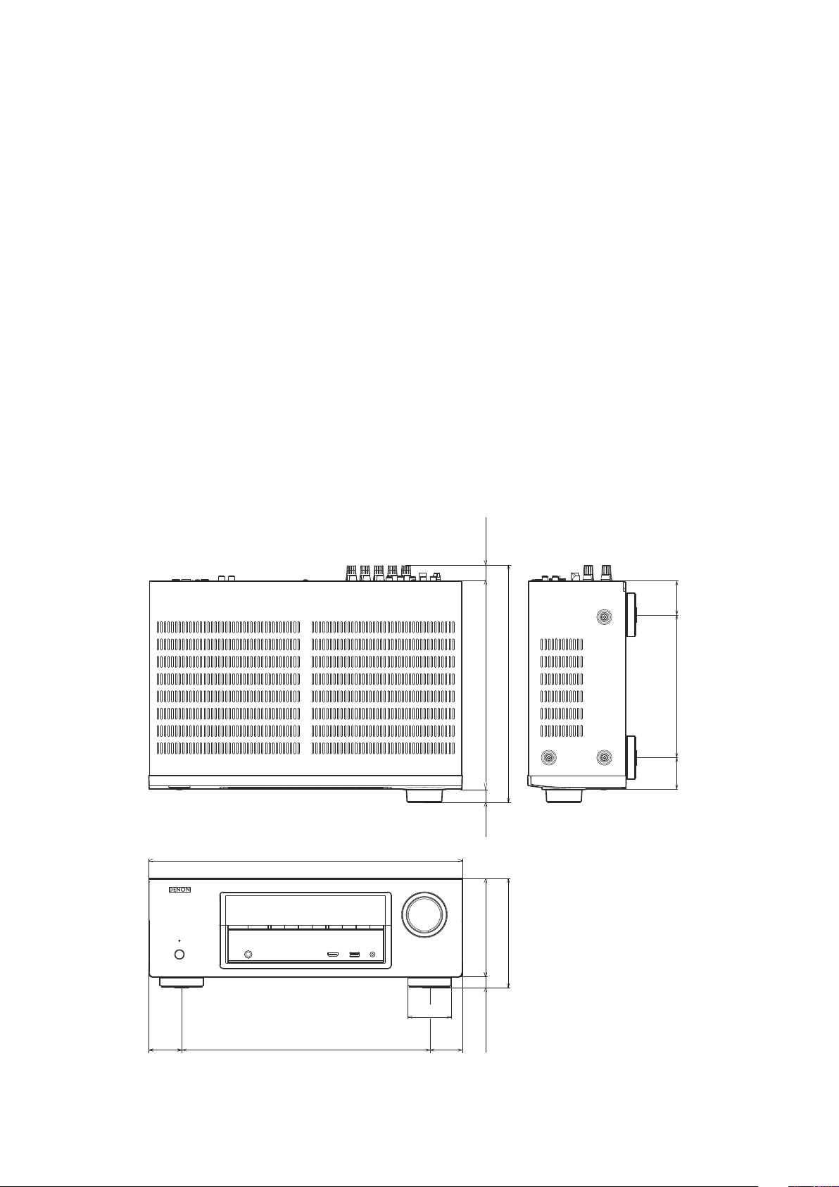
DIMENSION
CAUTION IN SERVICING
Initializing INTEGRATED NETWORK AV RECEIVER ..............9
Service Jig ................................................................................9
DISASSEMBLY
1. FRONT PANEL ASSY .........................................................12
2. DIGITAL PCB ASSY ............................................................13
3. RADIATOR ASSY ................................................................14
4. SMPS PCB ..........................................................................15
5. REGULATOR PCB ..............................................................15
6. TRANS POWER ..................................................................15
SPECIAL MODE
Special mode setting button ....................................................16
1. µcom/DSP Version display mode ........................................18
2. Errors checking mode (Displaying the protection history) ...21
3. Remote ID Setup mode .......................................................23
4. DIAGNOSTIC MODE
(Video/Audio (signal) path conrmation mode) ...................25
BLOCK DIAGRAM
WHEN THE MICROPROCESSOR IS
REPLACED WITH A NEW ONE
PROCEDURE FOR UPGRADING
THE VERSION OF THE FIRMWARE
1. How to update by DFW .......................................................39
2. How to update by DPMS .....................................................43
3. How to update by USB Memory ..........................................50
ADJUSTMENT
SURROUND MODES AND PARAMETERS
TROUBLE SHOOTING
1. POWER ...............................................................................62
2. Analog video ........................................................................63
3. HDMI/DVI ............................................................................64
4. AUDIO .................................................................................69
5. Network/USB .......................................................................72
6. SMPS ..................................................................................75
CLOCK FLOW & WAVE FORM IN DIGITAL BLOCK
LEVEL DIAGRAM
WIRING DIAGRAM
PRINTED WIRING BOARDS
MAIN .......................................................................................84
TUNER ....................................................................................86
POWER KNOB .......................................................................86
MIC ..........................................................................................86
HEADPHONE .........................................................................86
USB .........................................................................................86
FOR HDMI FFC CABLE ..........................................................86
FRONT ....................................................................................87
DIGITAL ...................................................................................88
F-HDMI ....................................................................................90
SMPS ......................................................................................90
REGULATOR ..........................................................................92
...............................................................................8
.........................................................................58
.............................................................3
..........................................................6
.........................................7
...........................................................7
................................................8
..........................................................9
........................................................................10
......................................................................16
...................................................................27
.............................................39
.....................................39
............................59
............................................................62
.............78
....................................................................79
..................................................................83
...................................................84
SCHEMATIC DIAGRAMS ........................................................93
FRONT PART ..........................................................................93
REGULATOR PART ................................................................94
SMPS UNIT .............................................................................95
MAIN PART .............................................................................96
ADV3002 PART .......................................................................97
HDMI PART .............................................................................98
DIGITAL SUPPLY PART ..........................................................99
MCU PART ............................................................................100
MCU_LEVEL_DHG PART .....................................................101
DIR PART ..............................................................................102
DSP PART .............................................................................103
MAIN DAC PART ..................................................................104
DM860_NETWORK PART ....................................................105
ETHERNET_PHY PART(1/2) ................................................106
ETHERNET_PHY PART(2/2) ................................................107
FRONT HDMI PART..............................................................108
AUDIO PART .........................................................................109
VIDEO PART .........................................................................109
EXPLODED VIEW
PARTS LIST OF EXPLODED VIEW
PACKING VIEW
PARTS LIST OF PACKING & ACCESSORIES
SEMICONDUCTORS
1. IC's ....................................................................................11 6
2. FL DISPLAY.......................................................................148
PARTS LIST OF P.C.B. UNIT
FRONT PCB UNIT ASS'Y .....................................................150
POWER PCB UNIT ASS'Y ....................................................154
MAIN PCB UNIT ASS'Y.........................................................157
DIGITAL PCB UNIT ASS'Y ....................................................163
..................................................................11 0
...................................... 111
.....................................................................11 4
.....................11 4
.............................................................11 6
................................................150
2
Page 3
ABOUT THIS MANUAL
Read the following information before using the service manual.
What you can do with this manual
Search for a Ref. No. (phrase)
(Ctrl+Shift+F)
You can use the search function in Acrobat Reader to
search for a Ref. No. in schematic diagrams, printed
wiring board diagrams, block diagrams, and parts lists.
1.Press Ctrl+Shift+F on the keyboard.
• The Search window appears.
F
Shift
Ctrl
2.Enter the Ref. No. you want to search for in the
Search window, and then click the Search button.
• A list of search results appears.
Jump to the target of a schematic diagram
connector
Click the Ref. No. of the target connector in the red box
around a schematic diagram connector.
• The screen jumps to the target connector.
3.Click an item on the list.
• The screen jumps to the page for that item, and
the search phrase is displayed.
• Page magnification stays the same as before the
jump.
3
Page 4
Using Adobe Reader (Windows version)
Add notes to this data (Sign)
The Sign function lets you add notes to the data in this
manual.
Save the le once you have nished adding notes.
[Example using Adobe Reader X]
On the "View" menu, click "Sign".
• The Sign pane appears.
[Example using Adobe Reader 9]
On the "Document" menu, click "Sign".
Magnify schematic / printed wiring board
diagrams - 1
(Ctrl+Space, mouse operation)
Press Ctrl+ Space on the keyboard and drag the
mouse to select the area you want to view.
• The selected area is magnied.
0
Ctrl Space
• When you want to move the area shown, hold down
Space and drag the mouse.
• When you want to show a full page view, press
Ctrl+0 on the keyboard.
Printamagniedpartofthemanual
The Properties dialog box and functions will vary depending on your printer.
1. Drag the mouse to magnify the part you want to print.
2. On the "
3. Congure the following settings in the Print dialog box.
File" menu, click "Print".
• Properties
Click this button and check that the printer is set to a
suitable paper size.
• Pagetoprint
Select the following checkbox.
More Options" : "Current View"
"
• PageSizing&Handling
Select the following checkbox.
Size" / "SizeOptions
"
" : "Fit"
4. Click the
Print button to start printing.
4
Page 5
Magnify schematic / printed wiring board
diagrams - 2
(Pan & Zoom function)
The Pan & Zoom function lets you see which part of a
magnied diagram is being shown in a separate window.
Magnify schematic / printed wiring board
diagrams - 3
(Loupe Tool function)
The Loupe Tool function lets you magnify a specific
part of a diagram in a separate window.
[Example using Adobe Reader X]
On the "View" menu, point to "Zoom", and then click
"Pan & Zoom".
• The Pan & Zoom window appears on the screen.
[Example using Adobe Reader X]
On the "View" menu, point to "Zoom", and then click
"Loupe Tool".
• The Loupe Tool window appears on the screen.
[Example using Adobe Reader 9]
On the "Tools" menu, point to "Select & Zoom", and
then click "Pan & Zoom Window".
[Example using Adobe Reader 9]
On the "Tools" menu, point to "Select & Zoom", and
then click "Loupe Tool Window".
5
Page 6

SAFETY PRECAUTIONS
The following items should be checked for continued protection of the customer and the service technician.
LEAKAGE CURRENT CHECK
Before returning the set to the customer, be sure to carry out either (1) a leakage current check or (2) a line to chassis
resistance check. If the leakage current exceeds 0.5 milliamps, or if the resistance from chassis to either side of the
power cord is less than 460 kohms, the set is defective.
Be sure to test for leakage current with the AC plug in both polarities, in addition, when the set's power is in each state (on,
off and standby mode), if applicable.
CAUTION
Please heed the following cautions and instructions during servicing and
inspection.
Heed the cautions!
◎
Cautions which are delicate in particular for servicing
are labeled on the cabinets, the parts and the chassis,
etc. Be sure to heed these cautions and the cautions
described in the handling instructions.
Cautions concerning electric shock!
◎
(1) An AC voltage is impressed on this set, so if
you touch internal metal parts when the set is
energized, you may get an electric shock. Avoid
getting an electric shock, by using an isolating
transformer and wearing gloves when servicing
while the set is energized, or by unplugging the
power cord when replacing parts, for example.
(2) There are high voltage parts inside. Handle with
extra care when the set is energized.
◎ Caution concerning disassembly and
assembly!
Through great care is taken when parts were
manufactured from sheet metal, there may be burrs
on the edges of parts. The burrs could cause injury if
ngers are moved across them in some rare cases.
Wear gloves to protect your hands.
Use only designated parts!
◎
The set's parts have specic safety properties (re
resistance, voltage resistance, etc.). Be sure to use
parts which have the same properties for replacement.
The burrs have the same properties. In particular, for
the important safety parts that are indicated by the z
mark on schematic diagrams and parts lists, be sure to
use the designated parts.
◎ Be sure to mount parts and arrange the wires
as they were originally placed!
For safety seasons, some parts use tapes, tubes or
other insulating materials, and some parts are mounted
away from the surface of printed circuit boards.
Care is also taken with the positions of the wires by
arranging them and using clamps to keep them away
from heating and high voltage parts, so be sure to set
everything back as it was originally placed.
Make a safety check after servicing!
◎
Check that all screws, parts and wires removed or
disconnected when servicing have been put back in
their original positions, check that no serviced parts
have deteriorate the area around. Then make an
insulation check on the external metal connectors and
between the blades of the power plug, and otherwise
check that safety is ensured.
(Insulation check procedure)
Unplug the power cord from the power outlet,
disconnect the antenna, plugs, etc., and on the power.
Using a 500V insulation resistance tester, check that
the insulation resistance value between the inplug and
the externally exposed metal parts (antenna terminal,
headphones terminal, input terminal, etc.) is 1MΩ or
greater. If it is less, the set must be inspected and
repaired.
CAUTION
Concerning important safety
parts
Many of the electric and the structural parts used in
the set have special safety properties. In most cases
these properties are difcult to distinguish by sight, and
the use of replacement parts with higher ratings (rated
power and withstand voltage) does not necessarily
guarantee that safety performance will be preserved.
Parts with safety properties are indicated as shown
below on the wiring diagrams and the parts list in this
service manual. Be sure to replace them with the parts
which have the designated part number.
(1) Schematic diagrams .......Indicated by the z mark.
(2) Parts lists .......Indicated by the z mark.
The use of parts other than the
designated parts could cause electric
shocks, res or other dangerous
situations.
6
Page 7

NOTE FOR SCHEMATIC DIAGRAM
WARNING:
Parts indicated by the z mark have critical characteristics. Use ONLY replacement parts recommended by the manufacturer.
CAUTION:
Before returning the set to the customer, be sure to carry out either (1) a leakage current check or (2) a line to chassis resistance check. If
the leakage current exceeds 0.5 milliamps, or if the resistance from chassis to either side of the power cord is less than 460 kohms, the set
is defective.
WARNING:
DO NOT return the set to the customer unless the problem is identied and remedied.
NOTICE:
ALL RESISTANCE VALUES IN OHM. k=1,000 OHM / M=1,000,000 OHM
ALL CAPACITANCE VALUES ARE EXPRESSED IN MICRO FARAD, UNLESS OTHERWISE INDICATED. P INDICATES MICRO-MICRO
FARAD. EACH VOLTAGE AND CURRENT ARE MEASURED AT NO SIGNAL INPUT CONDITION. CIRCUIT AND PARTS ARE SUBJECT
TO CHANGE WITHOUT PRIOR NOTICE.
NOTE FOR PARTS LIST
1.
Parts indicated by "nsp" on this table cannot be supplied.
2.
When ordering a part, make a clear distinction between "1" and "I" (i) to avoid mis-supplying.
3.
A part ordered without specifying its part number can not be supplied.
4.
Part indicated by "★" mark is not illustrated in the exploded view.
5.
General-purpose Carbon Film Resistor in the P.W.Board parts list. (Refer to the Schematic Diagram for those parts.)
6.
General-purpose Carbon Chip Resistors are not included are not included in the P.W.Board parts list.
(Refer to the Schematic Diagram for those parts.)
WARNING:
Parts indicated by the z mark have critical characteristics. Use ONLY replacement parts recommended by the manufacturer.
7
Page 8
TECHNICAL SPECIFICATIONS
Audio Section
n
• Poweramplier
Rated output :
Front : (for AVR-1613)
75 W + 75 W (8 Ω, 20 Hz – 20 kHz with 0.08 % T.H.D.)
120 W + 120 W (6 Ω, 1 kHz with 0.7 % T.H.D.)
Front : (for AVR-1713/1723)
80 W + 80 W (8 Ω, 20 Hz – 20 kHz with 0.08 % T.H.D.)
120 W + 120 W (6 Ω, 1 kHz with 0.7 % T.H.D.)
135 W + 135 W (6Ω, JEITA)
Center : (for AVR-1613)
75 W (8 Ω, 20 Hz – 20 kHz with 0.08 % T.H.D.)
120 W (6 Ω, 1 kHz with 0.7 % T.H.D.)
Center : (for AVR-1713/1723)
80 W (8 Ω, 20 Hz – 20 kHz with 0.08 % T.H.D.)
120 W (6 Ω, 1 kHz with 0.7 % T.H.D.)
135 W (6Ω, JEITA)
Surround : (for AVR-1613)
75 W + 75 W (8 Ω, 20 Hz – 20 kHz with 0.08 % T.H.D.)
120 W + 120 W (6 Ω, 1 kHz with 0.7 % T.H.D.)
Surround : (for AVR-1713/1723)
80 W + 80 W (8 Ω, 20 Hz – 20 kHz with 0.08 % T.H.D.)
120 W + 120 W (6 Ω, 1 kHz with 0.7 % T.H.D.)
135 W + 135 W (6Ω, JEITA)
Output connectors : 6 – 16 Ω
• Analog
Input sensitivity/Input impedance : 200 mV/47 kΩ
Frequency response: 10 Hz – 100 kHz — +1, –3 dB (DIRECT mode)
S/N : 98 dB (IHF–A weighted, DIRECT mode)
DIMENSION
Video section
n
• Standard video connectors
Input/output level and impedance : 1 Vp-p, 75 Ω
Frequency response: 5 Hz – 10 MHz — 0, –3 dB
Tuner section
n
[FM](Note: μV at 75 Ω, 0 dBf = 1 x 10
Receiving Range (for E3) :
[FM] 87.5 MHz – 107.9 MHz
Receiving Range (for E2/E1C) :
[FM] 87.5 MHz – 108.0 MHz
Usable Sensitivity :
[FM]1.2 μV (12.8 dBf)
50 dB Quieting Sensitivity :
[FM]MONO 2.8 μV (20.2 dBf)
S/N (IHF-A) :
[FM]MONO 70 dB (IHF–A weighted, DIRECT mode)
STEREO 67 dB (IHF–A weighted, DIRECT mode)
TotalharmonicDistortion(at1kHz):
[FM]MONO 0.7 %
STEREO 1.0 %
General
n
Power supply : (for E3) : AC 120 V, 60 Hz
(for E2) : AC 230 V, 50 Hz / 60Hz
(for E1C) : AC 220 V, 50 Hz
Power consumption : 360 W (for AVR-1613)
390 W (for AVR-1713/1723)
0.1 W (Standby)
–15
W)
434.0
344.0
Weight : 8.2kg (AVR-1613)
8.3kg (AVR-1713/1723)
60.0
288.5
329.0
198.043.5 47.0
18.5 22.0
136.0
151.0
15.0
45.045.0
8
Page 9
CAUTION IN SERVICING
InitializingINTEGRATEDNETWORKAVRECEIVER
INTEGRATED NETWORK AV RECEIVER initialization should be performed when the μcom, peripheral parts of μcom,
and Digital P.W.B. were replaced.
1. Turn off the power pressing
2. Press
3. Check that the entire display is ashing at intervals of about 1 second, and then release the 2 buttons.
The microprocessor will be initialized.
Note: • If step 3 fails, start over from step 1.
• All user settings will be lost and the factory setting will be recovered after the set is initialized.
button while simultaneously while pressing "SOURCE SELECT
X
So make sure to note down your setting beforehand for restoring after the initialization.
button.
X
"
and "SOURCE SELECT
0
1
SOURCE SELECT 0
X
SOURCE SELECT 1
"
buttons.
Service Jig
When you repair the printing board, you can use the following JIG (Extension cable kit).
Please order it from Denon Ofcial Service Distributor in your region if necessary.
8U-110084S
When you update the rmware by DFW, you can use the following JIG (RS232C to internal connector conversion adapter
with 4P FFC cable kit ).
Please order to Denon Ofcial Service Distributor in your region if necessary.
8U-210100S :
(Refer to 39 page.)
:
EXTENSION UNIT KIT : 1 Set
WRITING KIT : 1 Set
9
Page 10
DISASSEMBLY
• Disassemble in order of the arrow in the following gure.
• In the case of the re-assembling, assemble it in order of the reverse of the following ow.
• In the case of the reassembling, observe "Caution concerning disassembly and assembly!".
• If wire bundles are untied or moved to perform adjustment or replace parts etc., be sure to rearrange them neatly as
they were originally bundled or placed afterward.
Otherwise, incorrect arrangement can be a cause of noise generation.
TOP CABINET
FRONT PANEL ASSY
Refer to "DISASSEMBLY
1. FRONT PANEL ASSY"
and "EXPLODED VIEW"
FRONT PCB
(Ref. No. of EXPLODED VIEW : C1-1)
POWER KNOB PCB
(Ref. No. of EXPLODED VIEW : C1-2)
HEADPHONE PCB
(Ref. No. of EXPLODED VIEW : C1-3)
USB PCB
(Ref. No. of EXPLODED VIEW : C1-4)
MIC PCB
(Ref. No. of EXPLODED VIEW : C1-5)
F-HDMI PCB
(Ref. No. of EXPLODED VIEW : C3-2)
DIGITAL PCB ASSY
Refer to "DISASSEMBLY
2. DIGITAL PCB ASSY"
and "EXPLODED VIEW"
DIGITAL PCB
(Ref. No. of EXPLODED VIEW : C3-1)
TUNER PCB
(Ref. No. of EXPLODED VIEW : C2-5)
RADIATOR ASSY
Refer to "DISASSEMBLY
3. RADIATOR ASSY"
and "EXPLODED VIEW"
MAIN PCB
(Ref. No. of EXPLODED VIEW : C2-1)
SMPS PCB
Refer to "DISASSEMBLY
4. SMPS PCB"
and "EXPLODED VIEW"
SMPS PCB
(Ref. No. of EXPLODED VIEW : C4-1)
REGULATOR PCB
Refer to "DISASSEMBLY
5. REGULATOR PCB"
and "EXPLODED VIEW"
REGULATOR PCB
(Ref. No. of EXPLODED VIEW : C4-2)
TRANS POWER
Refer to "DISASSEMBLY
6. TRANS POWER"
and "EXPLODED VIEW"
TRANS POWER
(Ref. No. of EXPLODED VIEW : C6 )
10
Page 11
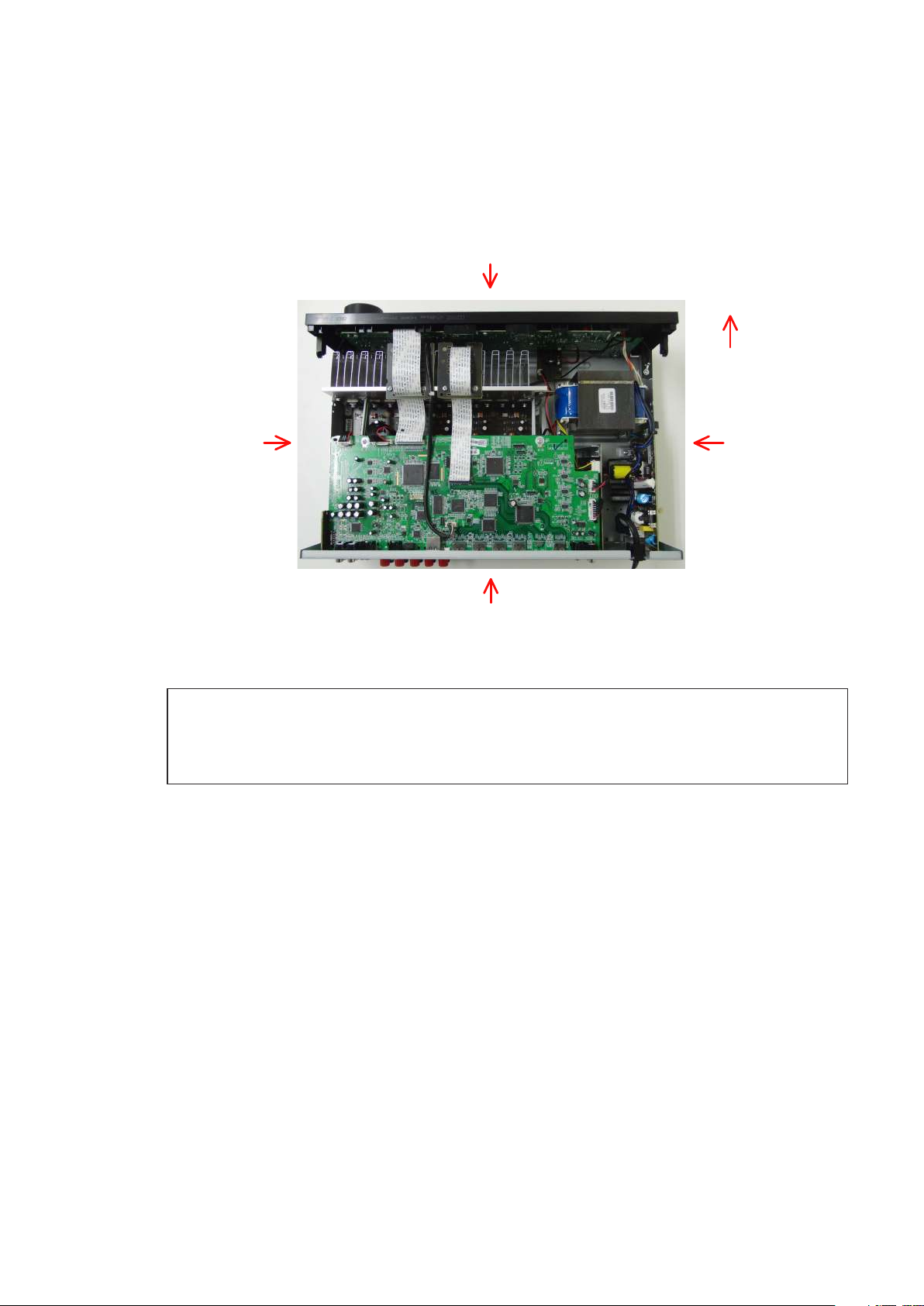
bout the photos used for "descriptions of the DISASSEMBLY" section
• The shooting direction of each photograph used herein is indicated on the left side of the respective photograph as
"Shooting direction: ***". (*** : A,B,C,D)
• Refer to the diagram below about the shooting direction of each photograph.
• Photographs with no shooting direction indicated were taken from the top of the set.
• The photograph is AVR-1613E3 model.
The viewpoint of each photograph
(Shooting direction)
Shooting direction: B
View from the top
Note: • Before disassembling this unit, be sure to discharge the power line (the colored line in the
schematic diagram).
• FFC cables with one end disconnected should be insulated by using tapes, etc.
Front side
Shooting direction: DShooting direction: C
Shooting direction: A
11
Page 12
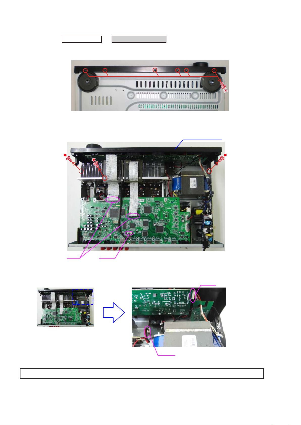
1. FRONT PANEL ASSY
Proceeding :
(1) Remove the screws.
View from the bottom
(2) Remove the screws and disconnect the FFC.
CABINET TOP
FRONT PANEL ASSY
FRONT PANEL ASSY
FFC
(3) Disconnect the connector wires.
Please refer to "EXPLODED VIEW" for the disassembly method of each PCB included in FRONT PANEL ASSY.
CN851
CN102
CN104
12
Page 13
2. DIGITAL PCB ASSY
Proceeding :
(1) Remove the screws.
Shooting direction: A
(2) Remove the screws.
Disconnect the connector wires and FFC then disconnect the TUNER PCB.
CN892
CABINET TOP
DIGITAL PCB ASSY
CN771
TUNER PCB
FFC
CN851
DIGITAL PCB
CN751
CN893
13
Page 14
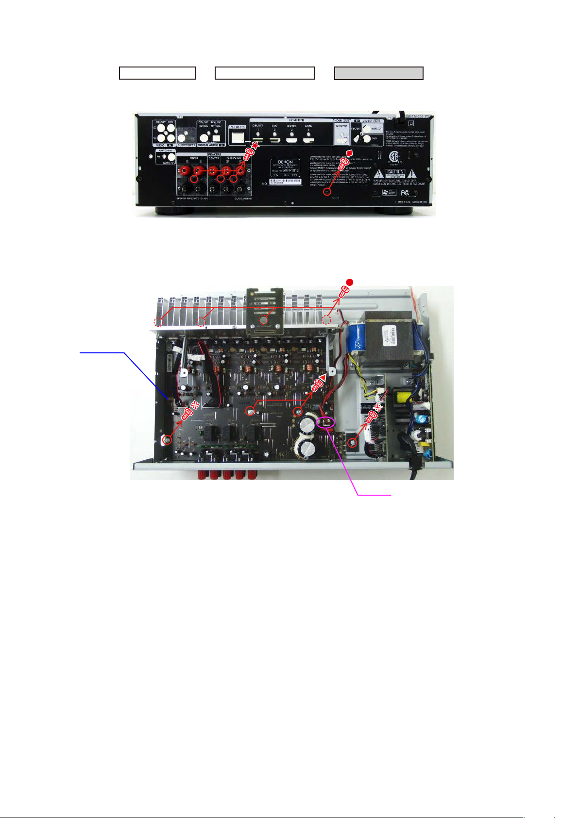
3. RADIATOR ASSY
Proceeding :
(1) Remove the screws.
Shooting direction: A
(2) Remove the screws then disconnect the connector wire.
Remove the RADIATOR ASSY from the CHASSIS BOTTOM.
MAIN PCB
CABINET TOP
DIGITAL PCB ASSY
RADIATOR ASSY
CN503
14
Page 15
4. SMPS PCB
Proceeding :
Please refer to "EXPLODED VIEW" for the disassembly method of SMPS PCB.
CABINET TOP
SMPS PCB
5. REGULATOR PCB
Proceeding :
Please refer to "EXPLODED VIEW" for the disassembly method of REGULATOR PCB.
CABINET TOP
REGULATOR PCB
6. TRANS POWER
Proceeding :
Please refer to "EXPLODED VIEW" for the disassembly method of TRANS POWER.
CABINET TOP
TRANS POWER
15
Page 16

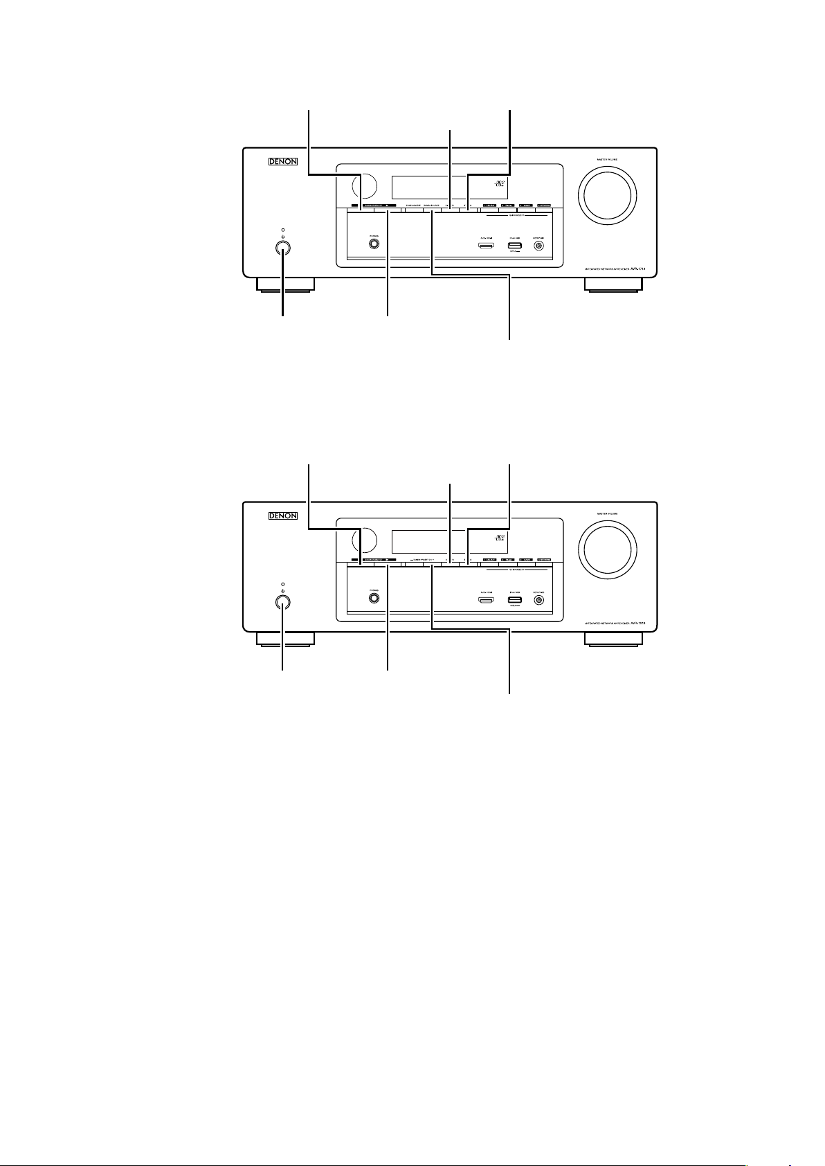
SPECIAL MODE
Special mode setting button
No.1 - 9 : Press the X button to turn on the power while pressing both the button A,B and the button C at the same time.
b
No.10 : Turn on the power, then press and hold down A and B buttons for over 3 second.
b
No. Mode Button A Button B Button C Contents
Version display
1
(μcom/DSP Error Display)
Displaying the protection history
2
mode
User Initialization mode
3
(Installer Setup settings are not
initialized.)
Mode for switching tuner
4
frequency step (E2 model Only)
Mode for preventing remote
5
control acceptance
6 Panel lock mode
Panel lock mode
7
(Master volume is not locked.)
8 Cancellation of panel lock mode
9 Diagnostic mode DIMMER STATUS
DIMMER STATUS -
DIMMER STATUS
SOURCE
SELECT
DIMMER
ZONE2
SOURCE
(AVR-1713E3)
TUNER
PRESET CH +
(Other model)
ZONE2
SOURCE
(AVR-1713E3)
TUNER
PRESET CH +
(Other model)
ZONE2
SOURCE
(AVR-1713E3)
TUNER
PRESET CH +
(Other model)
ZONE2
SOURCE
(AVR-1713E3)
TUNER
PRESET CH +
(Other model)
0
SOURCE
SELECT
SOURCE
SELECT
SOURCE
SELECT
SOURCE
SELECT
SOURCE
SELECT
SOURCE
SELECT
(AVR-1713E3)
PRESET CH +
1
1
1
1
1
1
(AVR-1713E3)
PRESET CH +
ZONE2
SOURCE
TUNER
(Other model)
ZONE2
SOURCE
TUNER
(Other model)
10 Remote ID Setup mode DIMMER STATUS -
-
-
-
-
-
-
Firmware versions such as Main or DSP are displayed in the
FL manager. Errors are displayed when they occur.
(Refer to 18 page)
The protection history is displayed.
(Refer to 21 page)
Backup data initialization is carried out.
(Installer Setup settings are not initialized.)
Change tuner frequency step to FM:200kHz/50kHz STEP.
Press the SOURCE SELECT 0/1 to select "Mode for
switching tuner frequency step", then press the "STATUS"
button to set.
Turn the power off in this state and turn the power on again to
make the setting take effect.
Operations using the remote control are rejected.
Press the SOURCE SELECT 0/1 to select "RC LOCK On",
then press the "STATUS" button to set.
(Mode cancellation: Execute the same button operations as
when performing setup and select "RC LOCK Off".)
Operations using the main unit panel buttons or the master
volume knob are rejected.
Press the SOURCE SELECT 0/1 to select "FP/VOL LOCK
On", then press the "STATUS" button to set.
Operations using the main unit panel buttons are rejected.
Press the SOURCE SELECT 0/1 to select "FP LOCK On",
then press the "STATUS" button to set.
Panel lock mode is cancelled.
(Mode cancellation: Execute the same button operations as
when performing setup and select "FP LOCK Off", then press
the "STATUS" button to set.)
This mode is used for conrming the Video and Audio signal
paths. (Troubleshooting)
The signal paths of the set can be easily conrmed after repair.
(Refer to 27 page)
When using multiple DENON AV receivers in the same room,
make this setting so that only the desired AV receiver operates.
(Refer to 23 page)
16
Page 17
AVR-1713E3
Other model
SOURCE SELECT 1
X
STATUSSOURCE SELECT 0
DIMMER
ZONE2 SOURCE
STATUSSOURCE SELECT 0
DIMMER
SOURCE SELECT 1
X
TUNER PRESET CH +
17
Page 18
1. µcom/DSP Version display mode
1.1. Operationspecications
µcom/DSP version display mode:
When the set is started up in this mode, the version information is displayed.
Starting up:
Press the X button to turn on the power while pressing the "STATUS" and "DIMMER" buttons.
Now, press the "STATUS" button to the display the 2nd item information on the FL Display.
When the version is displayed on the FL Display, the version list is also displayed on the GUI.
b
1.2. Display Order
Error information(Refer to 1.3. Error display) → q Model destination information → w Firmware Package Version
→ e Main µ-com → r Main 1st Boot Loader → t DSP ROM → y Audio PLD → u GUI SFLASH
→ *i Ethernet(DM860) 1st Boot Loader, Hardware ID → *o Ethernet(DM860) 2nd Boot Loader, Rhapsody Flag
→ *Q0 Ethernet(DM860) IMAGE → *Q1 Ethernet(DM860)MAC ADDRESS information
Model destination information :
q
Model FLD
AVR-1613 E3 model
AVR-1713 E3 model
AVR-1713 E2 model
AVR-1713 E1C model
AVR-1723 E1C model
Firmware Package Version :
w
FLD
P a c k a g e : * * * *
Main µ-com :
e
FLD
(*: Main version, #: Sub version)
Main 1st Boot Loader :
r
FLD
DSP ROM :
t
FLD
M a i n : * * * * # # # #
M a i n F B L : * * . * *
D S P : * * . * *
A V R 1 6 1 3 E 3
A V R 1 7 1 3 E 3
A V R 1 7 1 3 E 2
A V R 1 7 1 3 E 1 C
A V R 1 7 2 3 E 1 C
Audio PLD :
y
FLD
GUI SFLASH :
u
AVR-1613 E3 model
AVR-1713 E3 model
AVR-1713 E2 model
AVR-1713 E1C model
AVR-1723 E1C model
A u d i o P L D : * * . * *
Model FLD
G U I : 5 7 1 8 * * * *
G U I : 5 7 1 1 * * * *
G U I : 5 7 1 2 * * * *
G U I : 5 7 1 5 * * * *
G U I : 5 7 1 6 * * * *
18
Page 19
Ethernet(DM860) 1st Boot Loader, Hardware ID :
i
FLD
FLD
Ethernet(DM860) 2nd Boot Loader, Rhapsody Flag :
o
FLD
FLD
Ethernet(DM860) IMAGE :
Q0
FLD
FLD
E t h e r n e t F B L
Press the "STATUS" button.
* * * * * * - b d
E t h e r n e t S B L
Press the "STATUS" button.
B * * * * * * * * * * * * - 0 A
E t h e r n e t I M G
Press the "STATUS" button.
I * * * * * * * * * * * *
Ethernet(DM860)MAC ADDRESS information :
Q1
FLD
* E t h e r n e t M A C
Press the "STATUS" button.
FLD
* * * * * * - * * * * * * *
19
Page 20
1.3. Error display
See the following table for each "Error information" display and its explanation (status).
Display order is q,w,e,r,t.
Condition Status FL Display Trouble shooting
• Please check the
destination-resistors
R7663/R7664,
(
DIGITAL PCB).
• Please write the
rmware of correct
destination.
• Please check DIR
IC782, DIGITAL PCB)
(
and around circuits.
• Please check DSP
IC791, DIGITAL PCB)
(
and around circuits.
q
Firm Check
NG
w
DIR NG
e
DSP NG
r
EEPROM NG
t
Both DSP /
EEPROM OK
Compared with the destination setting
on the board. This is displayed when the
model name or destination information
written into the rmware does not match.
(b)
No response from DIR
When DSP code boot is performed, the
DSP FLAG0 port does not change to "H"
even if DSP reset is executed.
Before DSP command is issued, the DSP
FLAG0 port does not change to "H".
When DSP data read is performed,
executing WRITE="L" does not result in
ACK="H".
When DSP data read is performed,
executing REQ="L" does not result in
ACK="L".
When DSP data writing is performed,
executing WRITE="H" does not result in
ACK="H".
When DSP data writing is performed,
executing REQ="L" does not result in
ACK="L".
Error occurs in EEPROM checksum.(*** is
a block address number.)
F I R M E R R O R
D I R E R R O R 0 1
D S P E R R O R 0 1
D S P E R R O R 0 2
D S P E R R O R 0 3
D S P E R R O R 0 4
D S P E R R O R 0 5
D S P E R R O R 0 6
E 2 P R O M E R R * * *
(No error display, version display only)
Status FL Display
b
When the rmware version is displayed,
▲ is displayed at the start of the rmware.
–
M a i n : * * * * * * * *
–
D S P : * * . * *
–
A u d i o P L D : * * . * *
–
G U I : * * * * * * * *
20
Page 21

2. Errors checking mode (Displaying the protection history)
2.1. Operationspecications
Error mode (Displaying the protection history):
When the set is started up in this mode, the error information is displayed.
Starting up:
•Commoninallthemodels
Press the X button to turn on the power while pressing the "DIMMER", "STATUS" buttons and "ZONE2 SELECT"(only
AVR-1713E3)/ "TUNER PRESET CH +"(expect AVR-1713E3) button.
Press the SOURCE SELECT 0/1 to select "2.PROTECTION", then press the "STATUS" button to set.
The error (protection history display) mode is set.
Now, press the "STATUS" button to turn on the FL display.
2.2. About the display on the FL display
When the "STATUS" button is pressed after setting the error (protection history display) mode is set, a history like the one
shown below is displayed, depending on the conditions.
(1) Normal (when there has been no protection incident)
FLD
N O P R O T E C T
(2) For ASO (when the last protection incident was ASO protection)
FLD
P R T : A S O
Cause:
Supplementary information:
If the power is turned on without correcting the abnormality, the protection function will work about 6 seconds later
and the power supply will be shut off.
(3) For DC (when the last protection incident was DC protection)
Cause:
If the power is turned on without correcting the abnormality, the protection function will work about 6 seconds later
and the power supply will be shut off.
(4) For THERMAL (when the last protection incident was THERMAL(A) or THERMAL(B) protection)
Cause:
If the power is turned on without correcting the abnormality, the protection function will work about 2 minutes later
and the power supply will be shut off.
b
The line between speaker terminals is shorted, or speakers with impedance of less than the rated value.
As the excess current is detected after operation of the speaker relay, a short on the
speaker terminal and the connected speaker can be identied.
FLD
P R T : D C
DC output of the power amplier is abnormal.
FLD
P R T : T H E R M A L A
FLD
P R T : T H E R M A L B
The temperature of the heat sink is excessive.
Additional causes of protection can be due to loose connections, associated components, Microprocessor, etc.
When the "STATUS" button is pressed again after the above protection history as shown above is displayed, the normal
display reappears.
21
Page 22
2.3. Clearing the protection history
There are two ways to clear the protection history, as described below.
(1) Start up the set in error (protection display) mode and display the error, then press and hold down the "DIMMER"
button for 3 seconds.
FLD
P R T : D C
Press the "DIMMER" button for 3 seconds.
FLD
P R T : C L E A R
The above is displayed and the protection history is cleared.
FLD
N O P R O T E C T
(2) Initialize. (Refer to "Initializing INTEGRATED NETWORK AV RECEIVER" 9 page.)
If you want to save a backup, perform the method in 2.3.(1) above.
b
Warning indication by the POWER LED
If the power is turned off when a protection incident has been detected, the POWER LED (red) ashes as a warning
according to the conditions in which the protection incident occurred.
(1) ASO/DC PROTECTION : Flashes at intervals of 0.5 seconds (0.25 seconds lit, 0.25 seconds off)
(2) THERMAL (A/B) PROTECTION : Flashes at intervals of 2 seconds (1 second lit, 1 second off)
22
Page 23
3. Remote ID Setup mode
3.1. Specications
When using multiple DENON AV receivers in the same room, make this setting so that only the desired AV receiver
operates.
3.2. Setting the AV receivers
Starting up:
Press and hold both "STATUS" and "DIMMER" buttons for over 3 second with the power turned on.
(1) When Remote ID Setup mode is started, the following is displayed.
FLD
(2) Press the QUICK SELECT 1 - 4 button that corresponds to the number you want to set.
Button FL Display
R E M O T E I D ?
QUICK SELECT 1
QUICK SELECT 2
QUICK SELECT 3
QUICK SELECT 4
(3) Turn off the power using
(4) Turn on the power using
When Remote ID Setup mode is running, operations other than the QUICK SELECT 1 - 4 buttons or
b
the main unit are not received.
For the remote control that is supplied with this unit, you cannot change the REMOTE ID.
b
NOTE:
If the IDs do not match, "AVAMP z" (z is the main unit's remote control ID) appears on the display when the remote
control unit is operated.
button.
X
button.
X
R E M O T E I D 1
R E M O T E I D 2
R E M O T E I D 3
R E M O T E I D 4
buttons on
X
23
Page 24

Personal notes:
24
Page 25
4. DIAGNOSTICMODE(Video/Audio(signal)pathconrmationmode)
This mode is used for conrming the Video and Audio (signal) paths. (Troubleshooting)
Conrming the operation of unit can be easily done after repair.
Backup data will not be lost.
4.1. Starting diagnostic mode
Press the X button to turn on the power while pressing the "DIMMER", "STATUS" and "ZONE2 SELECT"(only AVR-1713E3)/ "TUNER PRESET CH +"(expect AVR-1713E3).
Press the SOURCE SELECT 0/1 to select "1.SERVICE CHECK", then press the "STA
TUNED, STEREO and RDS are lit in FL display.
4.2. Canceling diagnostic mode
Turn off the power by pressing the ON/Standby button.
4.3. Operation
When you perform remote operation in accordance with the instructions in "Details of how to operate remote controller" *a) in the table below using the remote control unit (RC-1156).
You will nd using another remote control unit with the macro functions very useful. To use the macro functions, program a macro function to output a remote control code in accordance with the steps in *b) in the table below.
4.4. Videosystemconrmationitems
g.XX : Refer to the block diagram of the g.XXth.
Conrmationitem Setting and display
Analog Video (signal) Path Display:
1
HDMI (signal) Path
g.1
V 0 1 D V D
Display:
V 0 1 D V D
2
g.2
TUS" button to set.
Details of how to operate remote controller *a)
1.Press [AMP]
2.Press [ZONE SELECT], Select "MAIN"
3.Press [1/./]
4.Press [DVD]
1.Press [AMP]
2.Press [ZONE SELECT], Select "MAIN"
3.Press [1/./]
4.Press [DVD]
Output sequence of remote control codes
※
q
Initialization
w
q
Initialization
w
It is useful to form a macro program. *b)
KEY 1/CODE1 (Main Zone)
DVD (Main Zone)
KEY 1/CODE1 (Main Zone)
DVD (Main Zone)
·Input : CVBS / Output : CVBS
·Input HDMI / Output : HDMI
(
Contentsofconrmation Remarks
As the input source, you can switch from DVD to other ones.)
b
OSD FUNCTION Menu : ON
Display:
3
V 0 2 D V D
g.3
CEC FUNCTION
(Control Monitor : HDMI Monitor)
4
HDMI Audio (signal) Path
(Audio : AMP)
5
HDMI Audio (signal) Path
(Audio : TV)
6
g.4
g.5a
g.5b
g.2
HDMI Control : ON
Display:
V 0 3 D V D
Audio : AMP(When checking the audio output
from AMP)
Display:
V 0 5 D V D
Audio : TV(When checking the audio output
from TV)
Display:
V 0 6 D V D
1.Press [AMP]
2.Press [ZONE SELECT], Select "MAIN"
3.Press [2/ABC]
4.Press [DVD]
5.Press [AMP]
6.Press [MENU]
1.Press [AMP]
2.Press [ZONE SELECT], Select "MAIN"
3.Press [3/DEF]
4.Press [DVD]
1.Press [AMP]
2.Press [ZONE SELECT], Select "MAIN"
3.Press [5/JKL]
4.Press [DVD]
1.Press [AMP]
2.Press [ZONE SELECT], Select "MAIN"
3.Press [6/MNO]
4.Press [DVD]
KEY 2/ABC (Main Zone)
q
Initialization
DVD (Main Zone)
w
GUI MENU (Main Zone)
e
KEY 3/DEF (Main Zone)
q
Initialization & CEC Control ON
DVD (Main Zone)
w
KEY 5/JKL (Main Zone)
q
Initialization & Select Audio AMP
DVD (Main Zone)
w
KEY 6/MNO (Main Zone)
q
Initialization & Audio Select TV
DVD (Main Zone)
w
·OSD Display / Output : HDMI
(b As the input source, you can switch from DVD to other ones.)
· When the power supply of a TV is put in the standby mode, make sure
that the power supply of this unit is also put in the standby mode.
(
As the input source, you can switch from DVD to other ones.)
b
·Input : HDMI (Signal of PCM, DolbyDigital or DTS) / Output : Speakers
·Input : HDMI (Signal of HD Audio) / Output : Speakers
(
As the input source, you can switch from DVD to other ones.)
b
· Input : HDMI (Signal of PCM or DolbyDigital or DTS) / Output : HDMI
(Audio output from connected TV)
(
As the input source, you can switch from DVD to other ones.)
b
25
Page 26
4.5. Audiosystemconrmationitems
g.XX : Refer to the block diagram of the g.XXth.
Conrmationitem Setting and display Details of how to operate remote controller
Analog (signal) Path Input Mode : Fixed ANALOG
SURROUND mode : DIRECT
1
g.6
Amp assign : NORMAL
Display:
A 0 1 D V D
1.Press [AMP]
2.Press [ZONE SELECT], Select "MAIN"
3.Press [7/PQRS]
4.Press [DVD]
Output sequence of remote control codes
It is useful to form a macro program.
b
KEY 7/PQRS (Main Zone)
q
Initialization & Amp assign NORMAL& Input Mode
Fixed ANALOG & SURROUND mode DIRECT
DVD (Main Zone)
w
Contentsofconrmation Remarks
·Input : Analog / Output : Speakers (Front L/R)
(b As the input source, you can switch from DVD to other ones.)
DIGITAL (signal) Path
(MAIN)
2
g.7
HDMI (signal) Path Input Mode : Fixed HDMI
3
g.8
A/D (signal) Path
(Main Zone)
4
g.9a
g.9b
Input Mode : Fixed DIGITAL
Amp assign : NORMAL
Display:
A 0 2 D V D
Amp assign : NORMAL
Display:
A 0 5 D V D
Amp assign : NORMAL
SURROUND mode : Multi ch STEREO
Vol -20dB
Speaker Cong : SSSSY
(Front/Center/Surround/SourroundBack : Small, SW : Yes)
Display:
A 0 6 D V D
1.Press [AMP]
2.Press [ZONE SELECT], Select "MAIN"
3.Press [8/TUV]
4.Press [DVD]
1.Press [AMP]
2.Press [ZONE SELECT], Select "MAIN"
3.Press [MOVIE]
4.Press [DVD]
1.Press [AMP]
2.Press [ZONE SELECT], Select "MAIN"
3.Press [MUSIC]
4.Press [DVD]
KEY 8/TUV (Main Zone)
q
Initialization & Amp assign NORMAL& Input Mode
Fixed DIGITAL
DVD (Main Zone)
w
MOVIE Select
q
Initialization &Amp assign NORMAL & Input Mode
Fixed HDMI
DVD (Main Zone)
w
MUSIC
q
Initialization &Amp assign NORMAL &
SURROUND mode : Multi ch STEREO & Volume
-20dB
DVD (Main Zone)
w
·Input : Digital / Output : Speakers (Front L/R)
(b As the input source, you can switch from DVD to other ones.)
·Input : HDMI / Output : Speakers (Front L/R)
(b As the input source, you can switch from DVD to other ones.)
·Input : Analog / Output : Speakers (Front L/R)
·Input : Analog / Output : SW(20Hz)
(
As the input source, you can switch from DVD to other ones.)
b
26
Page 27
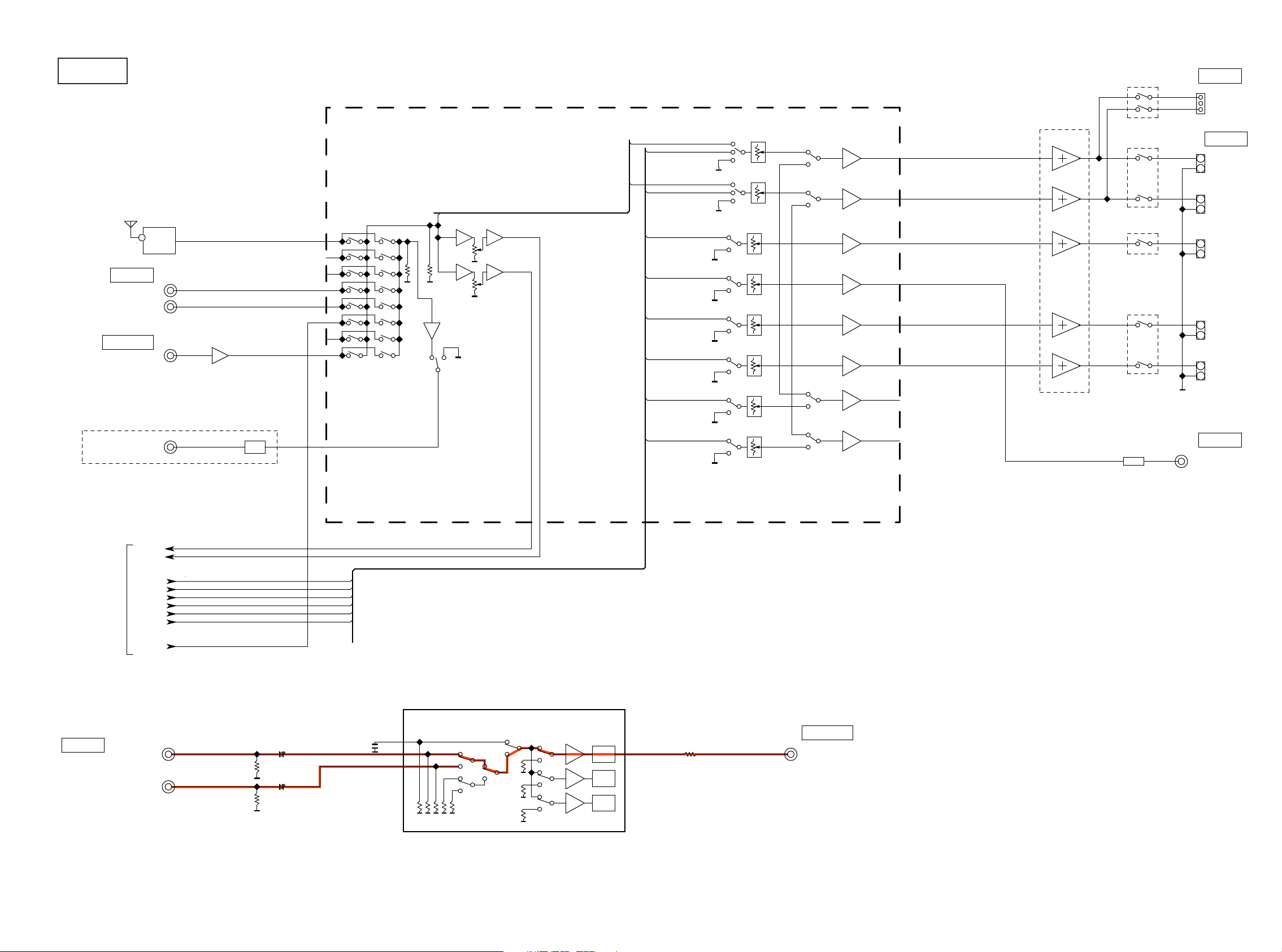
BLOCK DIAGRAM
g.1
MIC(AUTO SETU P)
AUDIO IN
DVD
SAT/CBL
AUDYSSEY
TUNER
FM ONLY
ANALOG AUDIO/VIDEO BLOCK
ANA01
DA02
ANA01
DA01
MAIN
ANA01
DA02
DA03
DA04
DA05
DA07
ANA_FL
DA_FL
ANA_FR
DA_FR
DA_CEN
DA_SW
DA_SL
DA_SR
DA_SBL
P-AMP
H/P OUT
H/P L
GND
H/P R
SPK OUT
+
FL
-
+
FR
-
+
CEN
-
+
SL
-
+
SR
-
AVR1713 E3 ONL Y
TO DIGITAL
AUDIO BLOCK
CVBS IN
ZONE2
AD_FL
AD_FR
DA_FL
DA_FR
DA_CEN
DA_SW
DA_SL
DA_SR
NETWORK
DVD
SAT/CBL
MUTE
DA01
DA02
DA03
DA04
DA05
DA06
NJM2595 IC901
20K
20K
20K
20K
6dB
6dB
6dB
75ohm
Driver
75ohm
Driver
75ohm
Driver
DA08
DA_SBR
IC891
PRE OUT
SWMUTE
VOL IC
NJU72340A
CVBS OUT
MONITOR OUT
27
Page 28
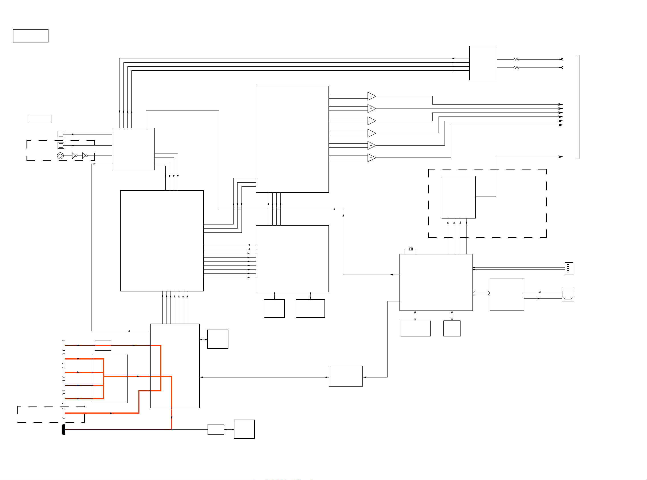
g.2
DIGTAL IN
OPTICAL IN1
OPTICAL IN2
COAXIAL IN1
JAPAN : OPT 2 / COAX NONE
OTHER : O
HDMI FRONT
HDMI IN1
HDMI IN2
HDMI IN3
HDMI IN4
PT NONE / COAX 1
DATAAD
LC89058W-E
HDMI_SPDIF
IC871
AD8195
IC711
ADV3002
VIDEO
SWITCHER
SCLK
MCLK
LRCLK
IC782
DIR
EPM3032ATC4410
HDMI_SPDIF
TRANSCEIVER
RMCK
RBCK
RLRCK
RDATA
IC783
PLD
MCK
LRCK
IC721
ADV7623
DIGITAL AUDIO/HDMI BLOCK
IC811
DATAAD
LRCLK
SCLK
MCLK
ADC
AK5358BET
IC812
DAC
AK4358VQ
DAC256fs
DAC64fs
DACfs
IC855
DAC
PCM5100
DATA0
DATA1
DATA2
DAC256fs
DAC64fs
DACfs
DSP1OUT64fs
DSP1OUTfs
DSP1IN64fs
DSP1INfs
DSP1IN0
DSP1IN1
DSP1IN2
DSP1IN3
DSPINMCK
SCLK
SD0
SD1
SD2
SD3
IC722
FLASH
32M
DATA3
IC791
DSP
ADSP21487KSWZ-2B
IC793 IC792
FLASH SDRAM
16M
64M
IC861
SLI11131
VIDEO ENCODER
VD0~7
24MHz
860SPDIF
CONTROLLER
VD0~7
FLASH
1G NAND Flash
MCLK
IC831
NETWORK
DM860A
IC833IC832
256M
SDRAM
LRCK
BLCK
AVR1713E3 ONLY
DATA
IC851
ETHERNET
PHY
LAN8720
AD_FL
AD_FR
DA_FL
DA_FR
DA_CEN
DA_SW
DA_SL
DA_SR
NETWORK
TO ANALOG
AUDIO BLOCK
USB
ETHERNET
AVR1713E3 ONL Y
HDMI IN5
HDMI OUT
CEC
IC761
CPU
28
Page 29
g.3
DIGTAL IN
OPTICAL IN1
OPTICAL IN2
COAXIAL IN1
JAPAN : OPT 2 / COAX NONE
OTHER : O
HDMI FRONT
PT NONE / COAX 1
HDMI IN1
HDMI IN2
HDMI IN3
HDMI IN4
DATAAD
LC89058W-E
HDMI_SPDIF
IC871
AD8195
IC711
ADV3002
VIDEO
SWITCHER
SCLK
MCLK
LRCLK
IC782
DIR
EPM3032ATC4410
HDMI_SPDIF
TRANSCEIVER
RMCK
RBCK
RLRCK
RDATA
IC783
PLD
MCK
LRCK
IC721
ADV7623
DIGITAL AUDIO/HDMI BLOCK
IC811
DATAAD
LRCLK
SCLK
MCLK
ADC
AK5358BET
IC812
DAC
AK4358VQ
DAC256fs
DAC64fs
DACfs
IC855
DAC
PCM5100
DATA0
DATA1
DATA2
DAC256fs
DAC64fs
DACfs
DSP1OUT64fs
DSP1OUTfs
DSP1IN64fs
DSP1INfs
DSP1IN0
DSP1IN1
DSP1IN2
DSP1IN3
DSPINMCK
SCLK
SD0
SD1
SD2
SD3
IC722
FLASH
32M
DATA3
IC791
DSP
ADSP21487KSWZ-2B
IC793 IC792
FLASH SDRAM
16M
64M
IC861
SLI11131
VIDEO ENCODER
VD0~7
24MHz
860SPDIF
CONTROLLER
VD0~7
FLASH
1G NAND Flash
MCLK
IC831
NETWORK
DM860A
IC833IC832
256M
SDRAM
LRCK
BLCK
AVR1713E3 ONLY
DATA
IC851
ETHERNET
PHY
LAN8720
AD_FL
AD_FR
DA_FL
DA_FR
DA_CEN
DA_SW
DA_SL
DA_SR
NETWORK
TO ANALOG
AUDIO BLOCK
USB
ETHERNET
AVR1713E3 ONL Y
HDMI IN5
HDMI OUT
CEC
IC761
CPU
29
Page 30
g.4
DIGTAL IN
OPTICAL IN1
OPTICAL IN2
COAXIAL IN1
JAPAN : OPT 2 / COAX NONE
OTHER : O
HDMI FRONT
HDMI IN1
HDMI IN2
HDMI IN3
HDMI IN4
PT NONE / COAX 1
DATAAD
LC89058W-E
HDMI_SPDIF
IC871
AD8195
IC711
ADV3002
VIDEO
SWITCHER
SCLK
MCLK
LRCLK
IC782
DIR
EPM3032ATC4410
HDMI_SPDIF
TRANSCEIVER
RMCK
RBCK
RLRCK
RDATA
IC783
PLD
MCK
LRCK
IC721
ADV7623
DIGITAL AUDIO/HDMI BLOCK
IC811
DATAAD
LRCLK
SCLK
MCLK
ADC
AK5358BET
IC812
DAC
AK4358VQ
DAC256fs
DAC64fs
DACfs
IC855
DAC
PCM5100
DATA0
DATA1
DATA2
DAC256fs
DAC64fs
DACfs
DSP1OUT64fs
DSP1OUTfs
DSP1IN64fs
DSP1INfs
DSP1IN0
DSP1IN1
DSP1IN2
DSP1IN3
DSPINMCK
SCLK
SD0
SD1
SD2
SD3
IC722
FLASH
32M
DATA3
IC791
DSP
ADSP21487KSWZ-2B
IC793 IC792
FLASH SDRAM
16M
64M
IC861
SLI11131
VIDEO ENCODER
VD0~7
24MHz
860SPDIF
CONTROLLER
VD0~7
FLASH
1G NAND Flash
MCLK
IC831
NETWORK
DM860A
IC833IC832
256M
SDRAM
LRCK
BLCK
AVR1713E3 ONLY
DATA
IC851
ETHERNET
PHY
LAN8720
AD_FL
AD_FR
DA_FL
DA_FR
DA_CEN
DA_SW
DA_SL
DA_SR
NETWORK
TO ANALOG
AUDIO BLOCK
USB
ETHERNET
AVR1713E3 ONL Y
HDMI IN5
HDMI OUT
CEC
IC761
CPU
30
Page 31

g.5a
DIGTAL IN
OPTICAL IN1
OPTICAL IN2
COAXIAL IN1
JAPAN : OPT 2 / COAX NONE
OTHER : O
HDMI FRONT
PT NONE / COAX 1
HDMI IN1
HDMI IN2
HDMI IN3
HDMI IN4
DATAAD
LC89058W-E
HDMI_SPDIF
IC871
AD8195
IC711
ADV3002
VIDEO
SWITCHER
SCLK
MCLK
LRCLK
IC782
DIR
EPM3032ATC4410
HDMI_SPDIF
TRANSCEIVER
RMCK
RBCK
RLRCK
RDATA
IC783
PLD
MCK
LRCK
IC721
ADV7623
DIGITAL AUDIO/HDMI BLOCK
IC811
DATAAD
LRCLK
SCLK
MCLK
ADC
AK5358BET
IC812
DAC
AK4358VQ
DAC256fs
DAC64fs
DACfs
IC855
DAC
PCM5100
DATA0
DATA1
DATA2
DAC256fs
DAC64fs
DACfs
DSP1OUT64fs
DSP1OUTfs
DSP1IN64fs
DSP1INfs
DSP1IN0
DSP1IN1
DSP1IN2
DSP1IN3
DSPINMCK
SCLK
SD0
SD1
SD2
SD3
IC722
FLASH
32M
DATA3
IC791
DSP
ADSP21487KSWZ-2B
IC793 IC792
FLASH SDRAM
16M
64M
IC861
SLI11131
VIDEO ENCODER
VD0~7
24MHz
860SPDIF
CONTROLLER
VD0~7
FLASH
1G NAND Flash
MCLK
IC831
NETWORK
DM860A
IC833IC832
256M
SDRAM
LRCK
BLCK
AVR1713E3 ONLY
DATA
IC851
ETHERNET
PHY
LAN8720
AD_FL
AD_FR
DA_FL
DA_FR
DA_CEN
DA_SW
DA_SL
DA_SR
NETWORK
TO ANALOG
AUDIO BLOCK
USB
ETHERNET
AVR1713E3 ONL Y
HDMI IN5
HDMI OUT
CEC
IC761
CPU
31
Page 32

g.5b
TUNER
FM ONLY
ANALOG AUDIO/VIDEO BLOCK
ANA01
DA02
ANA01
DA01
MAIN
ANA01
DA02
ANA_FL
DA_FL
ANA_FR
DA_FR
DA_CEN
P-AMP
H/P OUT
H/P L
GND
H/P R
SPK OUT
+
FL
-
+
FR
-
+
CEN
-
AUDYSSEY
MIC(AUTO SETU P)
AVR1713 E3 ONL Y
TO DIGITAL
AUDIO BLOCK
AUDIO IN
SAT/CBL
ZONE2
AD_FR
DVD
AD_FL
DA_FL
DA_FR
DA_CEN
DA_SW
DA_SL
DA_SR
MUTE
DA01
DA02
DA03
DA04
DA05
DA06
DA03
DA04
DA05
DA07
DA08
DA_SW
DA_SL
DA_SR
DA_SBL
DA_SBR
IC891
VOL IC
NJU72340A
+
SL
-
+
SR
-
PRE OUT
SWMUTE
CVBS IN
NETWORK
DVD
SAT/CBL
NJM2595 IC901
20K
20K
20K
20K
6dB
6dB
6dB
75ohm
Driver
75ohm
Driver
75ohm
Driver
CVBS OUT
MONITOR OUT
32
Page 33

g.6
TUNER
FM ONLY
ANALOG AUDIO/VIDEO BLOCK
ANA01
DA02
ANA01
DA01
MAIN
ANA01
DA02
ANA_FL
DA_FL
ANA_FR
DA_FR
DA_CEN
P-AMP
H/P OUT
H/P L
GND
H/P R
SPK OUT
+
FL
-
+
FR
-
+
CEN
-
AUDYSSEY
MIC(AUTO SETU P)
AVR1713 E3 ONL Y
TO DIGITAL
AUDIO BLOCK
AUDIO IN
SAT/CBL
ZONE2
AD_FR
DVD
AD_FL
DA_FL
DA_FR
DA_CEN
DA_SW
DA_SL
DA_SR
MUTE
DA01
DA02
DA03
DA04
DA05
DA06
DA03
DA04
DA05
DA07
DA08
DA_SW
DA_SL
DA_SR
DA_SBL
DA_SBR
IC891
VOL IC
NJU72340A
+
SL
-
+
SR
-
PRE OUT
SWMUTE
CVBS IN
NETWORK
DVD
SAT/CBL
NJM2595 IC901
20K
20K
20K
20K
6dB
6dB
6dB
75ohm
Driver
75ohm
Driver
75ohm
Driver
CVBS OUT
MONITOR OUT
33
Page 34

g.7
DIGTAL IN
OPTICAL IN1
OPTICAL IN2
COAXIAL IN1
JAPAN : OPT 2 / COAX NONE
OTHER : O
HDMI FRONT
HDMI IN1
HDMI IN2
HDMI IN3
HDMI IN4
PT NONE / COAX 1
DATAAD
LC89058W-E
HDMI_SPDIF
IC871
AD8195
IC711
ADV3002
VIDEO
SWITCHER
SCLK
MCLK
LRCLK
IC782
DIR
EPM3032ATC4410
HDMI_SPDIF
TRANSCEIVER
RMCK
RBCK
RLRCK
RDATA
IC783
PLD
MCK
LRCK
IC721
ADV7623
DIGITAL AUDIO/HDMI BLOCK
IC811
DATAAD
LRCLK
SCLK
MCLK
ADC
AK5358BET
IC812
DAC
AK4358VQ
DAC256fs
DAC64fs
DACfs
IC855
DAC
PCM5100
DATA0
DATA1
DATA2
DAC256fs
DAC64fs
DACfs
DSP1OUT64fs
DSP1OUTfs
DSP1IN64fs
DSP1INfs
DSP1IN0
DSP1IN1
DSP1IN2
DSP1IN3
DSPINMCK
SCLK
SD0
SD1
SD2
SD3
IC722
FLASH
32M
DATA3
IC791
DSP
ADSP21487KSWZ-2B
IC793 IC792
FLASH SDRAM
16M
64M
IC861
SLI11131
VIDEO ENCODER
VD0~7
24MHz
860SPDIF
CONTROLLER
VD0~7
FLASH
1G NAND Flash
MCLK
IC831
NETWORK
DM860A
IC833IC832
256M
SDRAM
LRCK
BLCK
AVR1713E3 ONLY
DATA
IC851
ETHERNET
PHY
LAN8720
AD_FL
AD_FR
DA_FL
DA_FR
DA_CEN
DA_SW
DA_SL
DA_SR
NETWORK
TO ANALOG
AUDIO BLOCK
USB
ETHERNET
AVR1713E3 ONL Y
HDMI IN5
HDMI OUT
CEC
IC761
CPU
34
Page 35

g.8
DIGTAL IN
OPTICAL IN1
OPTICAL IN2
COAXIAL IN1
JAPAN : OPT 2 / COAX NONE
OTHER : O
HDMI FRONT
PT NONE / COAX 1
HDMI IN1
HDMI IN2
HDMI IN3
HDMI IN4
DATAAD
LC89058W-E
HDMI_SPDIF
IC871
AD8195
IC711
ADV3002
VIDEO
SWITCHER
SCLK
MCLK
LRCLK
IC782
DIR
EPM3032ATC4410
HDMI_SPDIF
RMCK
RBCK
RLRCK
RDATA
IC783
PLD
MCK
LRCK
SCLK
SD0
SD1
SD2
SD3
IC721
ADV7623
TRANSCEIVER
DIGITAL AUDIO/HDMI BLOCK
IC812
DAC
AK4358VQ
DAC256fs
DAC64fs
DACfs
DATA0
DATA1
DATA2
DAC256fs
DAC64fs
DACfs
DSP1OUT64fs
DSP1OUTfs
DSP1IN64fs
DSP1INfs
DSP1IN0
DSP1IN1
DSP1IN2
DSP1IN3
DSPINMCK
IC722
FLASH
32M
DATA3
IC791
DSP
ADSP21487KSWZ-2B
IC793 IC792
FLASH SDRAM
16M
64M
IC861
SLI11131
VIDEO ENCODER
VD0~7
24MHz
860SPDIF
CONTROLLER
VD0~7
FLASH
1G NAND Flash
PCM5100
MCLK
IC831
NETWORK
DM860A
IC833IC832
256M
SDRAM
DATAAD
LRCLK
SCLK
MCLK
IC855
DAC
LRCK
BLCK
IC811
ADC
AK5358BET
AVR1713E3 ONLY
DATA
IC851
ETHERNET
PHY
LAN8720
AD_FL
AD_FR
DA_FL
DA_FR
DA_CEN
DA_SW
DA_SL
DA_SR
NETWORK
TO ANALOG
AUDIO BLOCK
USB
ETHERNET
AVR1713E3 ONL Y
HDMI IN5
HDMI OUT
CEC
IC761
CPU
35
Page 36

g.9a
TUNER
FM ONLY
ANALOG AUDIO/VIDEO BLOCK
ANA01
DA02
ANA01
DA01
MAIN
ANA01
DA02
ANA_FL
DA_FL
ANA_FR
DA_FR
DA_CEN
P-AMP
H/P OUT
H/P L
GND
H/P R
SPK OUT
+
FL
-
+
FR
-
+
CEN
-
AUDYSSEY
MIC(AUTO SETU P)
AVR1713 E3 ONL Y
TO DIGITAL
AUDIO BLOCK
AUDIO IN
SAT/CBL
ZONE2
AD_FR
DVD
AD_FL
DA_FL
DA_FR
DA_CEN
DA_SW
DA_SL
DA_SR
MUTE
DA01
DA02
DA03
DA04
DA05
DA06
DA03
DA04
DA05
DA07
DA08
DA_SW
DA_SL
DA_SR
DA_SBL
DA_SBR
IC891
VOL IC
NJU72340A
+
SL
-
+
SR
-
PRE OUT
SWMUTE
CVBS IN
NETWORK
DVD
SAT/CBL
NJM2595 IC901
20K
20K
20K
20K
6dB
6dB
6dB
75ohm
Driver
75ohm
Driver
75ohm
Driver
CVBS OUT
MONITOR OUT
36
Page 37

g.9b
DIGTAL IN
OPTICAL IN1
OPTICAL IN2
COAXIAL IN1
JAPAN : OPT 2 / COAX NONE
PT NONE / COAX 1
OTHER : O
HDMI FRONT
HDMI IN1
HDMI IN2
HDMI IN3
HDMI IN4
DATAAD
LC89058W-E
HDMI_SPDIF
IC871
AD8195
IC711
ADV3002
VIDEO
SWITCHER
SCLK
MCLK
LRCLK
IC782
DIR
EPM3032ATC4410
HDMI_SPDIF
TRANSCEIVER
RMCK
RBCK
RLRCK
RDATA
IC783
PLD
MCK
LRCK
IC721
ADV7623
DIGITAL AUDIO/HDMI BLOCK
IC811
DATAAD
LRCLK
SCLK
MCLK
ADC
AK5358BET
IC812
DAC
AK4358VQ
DAC256fs
DAC64fs
DACfs
IC855
DAC
PCM5100
DATA0
DATA1
DATA2
DAC256fs
DAC64fs
DACfs
DSP1OUT64fs
DSP1OUTfs
DSP1IN64fs
DSP1INfs
DSP1IN0
DSP1IN1
DSP1IN2
DSP1IN3
DSPINMCK
SCLK
SD0
SD1
SD2
SD3
IC722
FLASH
32M
DATA3
IC791
DSP
ADSP21487KSWZ-2B
IC793 IC792
FLASH SDRAM
16M
64M
IC861
SLI11131
VIDEO ENCODER
VD0~7
24MHz
860SPDIF
CONTROLLER
VD0~7
FLASH
1G NAND Flash
MCLK
IC831
NETWORK
DM860A
IC833IC832
256M
SDRAM
LRCK
BLCK
AVR1713E3 ONLY
DATA
IC851
ETHERNET
PHY
LAN8720
AD_FL
AD_FR
DA_FL
DA_FR
DA_CEN
DA_SW
DA_SL
DA_SR
NETWORK
TO ANALOG
AUDIO BLOCK
USB
ETHERNET
AVR1713E3 ONL Y
HDMI IN5
HDMI OUT
CEC
IC761
CPU
37
Page 38

POWER BLOCK DIAGRAM
!
MAIN+B
!
AC CORD
RELAY
!
S1(AMP+B,-B)
S2(+12V,-12V)
MAIN TRANS
S3(FL+ Vdisp)
2
4
1
3
50mA
NJM7812FA
MTZ7.5B
NJM2845DL133
KIA7805BPI
166.1mA
45mA
112mA
20.2mA
NJM7912FA
MTZ7.5B
KIA7805BPI
KIA7905PI
22mA
68mA
22mA
MAIN-B
VOLUME IC
(NJU72340A)
50mA
A+12V
(AZ4580,SPK RELAY)
145.1mA(44.2*3+ 12.5)
21mA
DA+3.3 V (PCM5100)
DA+5V
(AK4358VQ,AK5358)
85mA 27mA
AVR1713 E3 ONL Y
TUNER+5V
A-12V
VOLUME IC
(NJU72340A)
V+5V
(NJM2595)
22mA
V-5V
(NJM2595)
22mA
Vdisp(+37V)
45mA
S2 TOTAL : 437.3mA
!
163mA
S4(FILAMENT)
30mA
+5.2V
50.4mA
1000mA
6379.32mA
EX3AV(+3.3V)
D
G
12
3 4
S
MAIN PWR O N
EX3AV(+1.2V)
EX3AV(+1.8V)
EX3AV(+1.1V)
NJM2845DL133
1732.24mA
960mA
982mA
1304.62mA
110.06mA
695.22mA
743.02mA
294mA
960mA
982mA
1304.62mA
0.06mA
110mA
MCU+5V
CEC5V
(ADV3002,AD8195)
D5V/VBUS
DV5V/HDMI
DA3.3V/D IR,DSP
(ADSP21487,W9864G6JH ,EPM3032,LC89058,TC 74VHCU04,MX29LV160)
CEC3V3/HDM I
(ADV7623,
NET3.3V/ NETWOR K
(DM860A , SLI11131 , W9825G6 JH-6 , H27U1G 8F2BTR-BC , LAN8720ACP TR)
NET1.2V/ NETWOR K
(DM860A,SLI11131)
+1V8H/ HDMI
(ADV7623)
SWM3.3V /LEVEL_CHG
(SN74LVC244APWR ,TC74VHC08)
MCU_3V3/MICOM
(R5F56108VNFP ,R1EX24256BSAS0A,VFD)
(CVDBLB JEGJ204L)FRONT LED
30mA
20.4mA
30mA
0.2mA 400mA 225mA 40mA 0.02mA
MX25L3206E,ADV 3002,AD8195,TC74VHC4051A FT)
314mA 25mA
70mA 60mA
610mA
350mA
982mA
DA1.1V/D SP
(ADSP21487)
1304.62mA
170mA
80mA
TOTAL : 960mA
TOTAL : 982mA
TOTAL:1304.62mA
TOTAL : 1080.4mA
234mA
0.02mA
TOTAL : 110.06mA
0.04mA
100mA 5mA
0.02mA
5mA
30mA 54mA
FILAMENT AC
FILAMENT AC
SMPS TOTAL : 6169.32mA
30mA
TOTAL : 1732.24mA
38
Page 39

WHEN THE MICROPROCESSOR IS REPLACED WITH A NEW ONE
When the U-PRO (Microprocessor) or the Flash ROM is replaced, conrm the following.
PWB Name Ref. No. Description
DIGITAL IC761 R5F56108VNFP B SOFTWARE: Main
DIGITAL IC793 MX29LV160DBTI-70G B SOFTWARE: DSP ROM
DIGITAL IC783 EPM3032A-TC4410 B SOFTWARE: AUDIO PLD
DIGITAL IC722 MX25L3206EM2I-12G B SOFTWARE: OSD ROM
After
replaced
Remark
After replacing
A
: Mask ROM (With software). No need for write-in of software to the microprocessor.
B
: Flash ROM (With software). Usually, no need for write-in of software. But, when the software was updated, you should
write the new software on the microprocessor or ash ROM. Please check the software version.
C
: Empty Flash ROM (Without software). You should write the software on the microprocessor or ash ROM.
Refer to "Update procedure" or "writing procedure", when you write the software.
PROCEDURE FOR UPGRADING THE VERSION OF THE FIRMWARE
1. How to update by DFW
1.1. Preparations before starting the operation
(1) Personal Computer (Installed "DFW_0057_AVR1713_1723_1613(Rev.2.1.5).exe".
(2) RS-232 cable (9P (Male ), Straight).
(3) 8U-210100 Writing Kit.
1.2. Connection of AV receiver
(1) Conrm the power on/off switch of the AV receiver is turning off.
(2) Connect the update terminal of AV receiver with the "Writing Kit".
(3) Connect the RS-232C cable from PC with the "Writing Kit".
4P FFC Cable
This side is contacts of
flexible card cable.
Writing Kit
S706-709 : No Preference
S709
S708
S707
RS-232C Cable
S706
S702 : 3.3V
S702
PC
39
Page 40

1.3. Turn on the AV receiver
Operate the following. Turn on the AV receiver.
(1) Connect the power cable to the AC outlet while simultaneously pushing the "SOURCE SELECT
"
SELECT
the front panel.
(2) Conrm the power indicator is green and "WRITTING" is displayed in the front panel.
and the "ZONE2 SELECT"(only AVR-1713E3)/ "TUNER PRESET CH +"(expect AVR-1713E3) button of
1
1.4. Run the DFW
Run the "DFW_0057_AVR1713_1723_1613(Rev.2.1.5).exe" on desktop of PC.
1.5. Communication check
(1) Select the serial port number of RS-232C in PC.
(2) Click the "Check Comm." button.
"
, "SOURCE
0
2
1
(3) When connection is good, then you can see the "Communication check OK." message.
(4) If connection is not good, then you can see the "Communication check NG" message.
Please conrm the following
(a) Check the connection of the AV receiver and PC. (refer to "
(b) Check the operation mode of the AV receiver. (refer to "
(c) Check the selection of the RS-232C port number of PC.
1.3.Turn on the AV receiver")
40
1.2. Connection of the AV receiver" )
Page 41

1.6. Downloadthermware
(1) Click the "Load" button.
(2) Download the rmware from the specied download source to PC.
XXX-XXXX
XXX-XXXX_WWWXXXXYYYY-ZZZZ.bin
XXX-XXXX_WWWXXXXYYYY-ZZZZ.bin
1.7. Completethermwareupdating
(1) Click the "Update" button.
XXXXXXX
(2) When writing of the rmware is completed, the power of AV receiver turns on automatically and you can see the
"Update completed" message.
XXXXXXXX
41
Page 42

(3) If you can’t complete the rmware update, please retry the rmware update from "1.3. Turn on the AV receiver".
1.8. Notice:
Please keep the following notice for rmware update.
(a) Keep the PC environment
(b) Avoid the communication cable from the electrical noise source.
(e.g. telephone cable, AC line, a uorescent light)
(c) Don’t remove cable during update.
(d) Don’t turn off the power during update.
(e) Don’t run other PC application during update.
(f) Stop the resident program on PC (Virus checker and System check utility, etc)
(g) Stop the screen saver on PC.
(h) Stop the power save ability on PC.
(i) In case of laptop PC, Use the AC adaptor.
Conrmingthermware’snumberafterupgraded
After updating the rmware, check the version. Refer to "
1.μcom/DSPVersiondisplaymode
" (18 page).
42
Page 43

2. How to update by DPMS
You can update the rmware by downloading the latest version from the Internet.
2.1. Connecting to the Network
(1) System requirements
• Internet Connection by Broadband Circuit
• Modem
• Router
• Ethernet cable (CAT-5 or greater recommended)
(2) Setting
Internet
Computer
Modem
LAN port/
Ethernet
connector
Router
To WAN port
To LAN port
To LAN port
ETHERNET
connector
2.2. Checkingandupdatingthermware
Check if the latest rmware exists. You can also check approximately time required to complete an update.
(1) Press the SETUP button on the remote control to display the GUI menu.
(2) Use the cursor buttons to select "General" → "Firmware" → "Update" → "Check for Update".
(3) Press the ENTER button.
• The latest version of the rmware on the website is displayed.
• If the rmware on the website is latest, proceed to (4).
• If the latest rmware has been already installed, press the SETUP button to close the menu.
(4) Use the cursor buttons to select "Start", then press the ENTER button.
• During update, the power indicator lights in red and the GUI screen disappears. And an approximately remaining
time is indicated on the display.
• When updating is complete the power indicator lights in green and normal status is resumed.
--- Cautions on Firmware Update ---
• In order to update the rmware, you must have the correct system requirements and settings for a broadband Internet
connection.
• Do not turn off the power until updating is completed.
• Even with a broadband connection to the Internet, approximately 1 hour is required for the updating procedure to be
completed.
Once updating starts, normal operations on the this unit cannot be performed until updating is completed. Also, setting
items of the GUI menu of this unit or setting items of the image adjustment may be initialized.
Note down the settings before updating, and set them again after updating.
43
Page 44

2.3. About the error code
See the table below for error codes, details of faults, and coping strategies when the rmware is updated through DPMS
(Denon Product Management Server).
Error
Code
01 Log-in to DPMS failed.
02
03 Connection to DPMS failed.
04
05
06
07
Details of Error code Display Coping strategies
Line, etc., is busy when logging into
DPMS.
Firmware le data was requested but
error message was received.
Firmware le data was requested but
it timed out.
Firmware le data was requested but
error message was received.
All rmware le data was requested
but it timed out.
L o g i n f a i l e d 0 1
S e r v e r i s b u s y 0 2
C o n n e c t i o n F a i l 0 3
C o n n e c t i o n F a i l 0 4
C o n n e c t i o n F a i l 0 5
C o n n e c t i o n F a i l 0 6
C o n n e c t i o n F a i l 0 7
Reset and update again.
Carry out the update in an environment
that has little network load.
Carry out the update in an environment
that has little network load.
Check the network connection.
Carry out the update in an environment
that has little network load.
Check the network connection.
Carry out the update in an environment
that has little network load.
Check the network connection.
Carry out the update in an environment
that has little network load.
Check the network connection.
Carry out the update in an environment
that has little network load.
Check the network connection.
Carry out the update in an environment
that has little network load.
Firmware le data of Main CPU was
08
requested but error message was
received.
Firmware le data of Main CPU was
09
requested but it timed out.
Error (NG) message was received
0A
when rmware of Main CPU was
downloaded.
Error (line congestion) message was
0B
received when rmware of Main CPU
was downloaded.
Error (connection failure) message
0C
was received when rmware of Main
CPU was downloaded.
0D Received Package Version is wrong.
Connection to DPMS failed.
0E
(can not get NTP)
C o n n e c t i o n F a i l 0 8
C o n n e c t i o n F a i l 0 9
D o w n l o a d f a i l 0 A
D o w n l o a d f a i l 0 B
D o w n l o a d f a i l 0 C
D o w n l o a d f a i l 0 D
C o n n e c t i o n F a i l 0 E
Check the network connection.
Carry out the update in an environment
that has little network load.
Check the network connection.
Carry out the update in an environment
that has little network load.
Check the network connection.
Carry out the update in an environment
that has little network load.
Check the network connection.
Carry out the update in an environment
that has little network load.
Check the network connection.
Carry out the update in an environment
that has little network load.
Check the network connection.
Carry out the update in an environment
that has little network load.
Check the network connection.
Carry out the update in an environment
that has little network load.
Main CPU failed to receive rmware
10
for rewriting sent from
DM860A (when timed out).
U p d a t i n g f a i l 1 0
44
Turn off and on the power. Updating
starts automatically.
Page 45

Error
Code
Details of Error code Display Coping strategies
Main CPU failed to receive rmware
11
for rewriting sent from DM860A (when
an error occurred).
There was invalid data in the rmware
for rewriting sent from DM860A to
12
Main CPU (when a Check Sum error
occurred).
The deletion of block data failed
13
before Main CPU was rewritten.
The rewriting of block data failed
14
when Main CPU was rewritten.
The data verication was invalid after
15
Main CPU was rewritten.
Failure to acquire (Boot Loader Mode)
20
IP address before rewriting DM860A
(AutoIP).
Failure to acquire (Boot Loader Mode)
21
IP address before rewriting DM860A
(when timed out).
U p d a t i n g f a i l 1 1
U p d a t i n g f a i l 1 2
E r a s e f a i l 1 3
U p d a t i n g f a i l 1 4
U p d a t e C h e c k N G 1 5
C o n n e c t i o n F a i l 2 0
C o n n e c t i o n F a i l 2 1
Turn off and on the power.
Updating starts automatically.
Turn off and on the power.
Updating starts automatically.
Turn off and on the power.
Updating starts automatically.
Turn off and on the power.
Updating starts automatically.
Turn off and on the power.
Updating starts automatically.
Check the network connection.
Carry out the update in an environment
that has little network load.
Check the network connection.
Carry out the update in an environment
that has little network load.
22 Log-in to DPMS failed.
Line, etc., is busy when logging into
23
DPMS.
24 Connection to DPMS failed.
25 Mode change failure of DM860A.
Data acquisition failed (timed out)
when rmware of Main CPU was
26
downloaded. Received Package
Version is wrong.
27 Mode change failure of DM860A.
Log-in to DPMS failed when Main
36
CPU was rewritten.
L o g i n f a i l e d 2 2
S e r v e r i s b u s y 2 3
C o n n e c t i o n F a i l 2 4
C o n n e c t i o n F a i l 2 5
D o w n l o a d f a i l 2 6
D o w n l o a d f a i l 2 7
L o g i n f a i l e d 3 6
Reset and update again.
Carry out the update in an environment
that has little network load.
Carry out the update in an environment
that has little network load.
Check the network connection.
Carry out the update in an environment
that has little network load.
Reset and update again.
Check the network connection.
Carry out the update in an environment
that has little network load.
Reset and update again.
Carry out the update in an environment
that has little network load.
Line, etc., is busy when logging
37
into DPMS when Main CPU was
rewritten.
Connection to DPMS failed when
38
Main CPU was rewritten.
S e r v e r i s b u s y 3 7
C o n n e c t i o n F a i l 3 8
45
Carry out the update in an environment
that has little network load.
Check the network connection.
Carry out the update in an environment
that has little network load.
Page 46

Error
Code
Details of Error code Display Coping strategies
Connection to DPMS timed out
39
when Main CPU was rewritten.
Error (NG) message was received
3A
when rmware was downloaded or
Main CPU was rewritten.
Error (line congestion) message
3B
received when downloading rmware
when Main CPU was rewritten.
Error (connection failure) message
3C
received when downloading rmware
when Main CPU was rewritten.
Failure to acquire (Boot Loader Mode)
3D
IP address before rewriting DM860A
(AutoIP).
Failure to acquire (Boot Loader Mode)
3E
IP address before rewriting DM860A
(when timed out).
Log-in to DPMS failed when rmware
50
such as DSP and PLD was rewritten.
C o n n e c t i o n F a i l 3 9
D o w n l o a d f a i l 3 A
D o w n l o a d f a i l 3 B
D o w n l o a d f a i l 3 C
C o n n e c t i o n F a i l 3 D
C o n n e c t i o n F a i l 3 E
L o g i n f a i l e d 5 0
Check the network connection.
Carry out the update in an environment
that has little network load.
Turn off and on the power.
Updating starts automatically.
Carry out the update in an environment
that has little network load.
Turn off and on the power.
Updating starts automatically.
Carry out the update in an environment
that has little network load.
Turn off and on the power.
Updating starts automatically.
Carry out the update in an environment
that has little network load.
Check the network connection.
Carry out the update in an environment
that has little network load.
Check the network connection.
Carry out the update in an environment
that has little network load.
Carry out the update in an environment
that has little network load.
Line, etc., is busy when the log-in to
51
DPMS when rmware such as DSP
and PLD was rewritten.
Connection to DPMS failed when
52
rmware such as DSP and PLD was
rewritten.
Error message received regarding
rmware data after the log-in to
54
DPMS when rmware such as DSP
and PLD was rewritten.
When rmware such as DSP and
PLD was rewritten, request was made
55
for rmware data after the log-in to
DPMS, but it timed out.
Downloading rmware failed after the
56
log-in to DPMS when rmware such
as DSP and PLD was rewritten.
Firmware download error received
(line congestion) after the log-in to
57
DPMS when rmware such as DSP
and PLD was rewritten.
Firmware download error received
(connection failure) after the log-in to
58
DPMS when rmware such as DSP
and PLD was rewritten.
S e r v e r i s b u s y 5 1
C o n n e c t i o n F a i l 5 2
U p d a t i n g f a i l 5 4
U p d a t i n g f a i l 5 5
D o w n l o a d f a i l 5 6
D o w n l o a d f a i l 5 7
D o w n l o a d f a i l 5 8
Carry out the update in an environment
that has little network load.
Check the network connection.
Carry out the update in an environment
that has little network load.
Turn off and on the power.
Updating starts automatically.
Carry out the update in an environment
that has little network load.
Turn off and on the power.
Updating starts automatically.
Carry out the update in an environment
that has little network load.
Turn off and on the power.
Updating starts automatically.
Carry out the update in an environment
that has little network load.
Turn off and on the power.
Updating starts automatically.
Carry out the update in an environment
that has little network load.
Turn off and on the power.
Updating starts automatically.
Carry out the update in an environment
that has little network load.
NACK was received when "C"
5A
command sent to DSP, PLD etc.
NACK was received when "L"
5B
command sent to DSP, PLD etc.
C o n n e c t i o n F a i l 5 A
U p d a t i n g f a i l 5 B
46
Turn off and on the power.
Updating starts automatically.
Turn off and on the power.
Updating starts automatically.
Page 47

Error
Code
Details of Error code Display Coping strategies
DSP, PLD etc. failed to receive
5C
rmware for rewriting sent from
DM860A (when timed out).
DSP, PLD etc. failed to receive
5D
rmware for rewriting sent from
DM860A (when an error occurred).
Data in rmware such as DSP and
PLD for rewriting sent from DM860A
5E
was invalid (when a Check Sum error
occurred).
Invalid data in rmware such as
DSP and PLD for rewriting sent from
5F
DM860A was invalid (invalid data was
received).
NACK was received when "P"
60
command sent to DSP, PLD etc.
NACK was received when "I"
61
command sent to DSP, PLD etc.
Acquisition of serial ash data failed
80
before serial ash was deleted.
U p d a t i n g f a i l 5 C
U p d a t i n g f a i l 5 D
U p d a t i n g f a i l 5 E
U p d a t i n g f a i l 5 F
U p d a t i n g f a i l 6 0
U p d a t e C h e c k N G 6 1
U p d a t i n g f a i l 8 0
Turn off and on the power.
Updating starts automatically.
Turn off and on the power.
Updating starts automatically.
Turn off and on the power.
Updating starts automatically.
Turn off and on the power.
Updating starts automatically.
Turn off and on the power.
Updating starts automatically.
Turn off and on the power.
Updating starts automatically.
Turn off and on the power.
Updating starts automatically.
Deleting data failed before serial ash
81
was rewritten.
Receiving rmware for rewriting serial
82
ash sent by DM860A failed (when
timed out).
Receiving rmware for rewriting serial
83
ash sent by DM860A failed (when an
error).
Receiving rmware for rewriting serial
84
ash sent by DM860A failed (when a
Check Sum error).
Receiving rmware for rewriting serial
85
ash sent by DM860A failed (when
invalid data was received).
The data verication was invalid after
86
serial ash was rewritten.
Acquisition of (Application Mode) IP
A0
address failed before DM860A was
rewritten (AutoIP).
U p d a t i n g f a i l 8 1
U p d a t i n g f a i l 8 2
U p d a t i n g f a i l 8 3
U p d a t i n g f a i l 8 4
U p d a t i n g f a i l 8 5
U p d a t i n g f a i l 8 6
C o n n e c t i o n F a i l A 0
Turn off and on the power.
Updating starts automatically.
Turn off and on the power.
Updating starts automatically.
Turn off and on the power.
Updating starts automatically.
Turn off and on the power.
Updating starts automatically.
Turn off and on the power.
Updating starts automatically.
Turn off and on the power.
Updating starts automatically.
Check the network connection.
Carry out the update in an environment
that has little network load.
Acquisition of (Application Mode) IP
A1
address failed before DM860A was
rewritten (when timed out).
Invalid login via DPMS access
was notied when DM860A related
A2
rmware was rewritten (Application
Mode).
C o n n e c t i o n F a i l A 1
L o g i n f a i l e d A 2
47
Check the network connection.
Carry out the update in an environment
that has little network load.
Check the network connection.
Carry out the update in an environment
that has little network load.
Page 48

Error
Code
A3
A4
A6
A7
AE
AF
B0
B1
B2
B3
Details of Error code Display Coping strategies
Line congestion via DPMS access
was notied when DM860A related
rmware was rewritten (Application
Mode).
Connection failure via DPMS access
was notied when DM860A related
rmware was rewritten (Application
Mode).
Firmware data error message was
received after DPMS login when
DM860A related rmware was
rewritten (Application Mode).
When DM860A related rmware was
rewritten (Application Mode), request
was made for rmware data after
DPMS login but it timed out.
Firmware download error message
received (when download fails)
when DM860A related rmware was
rewritten (Boot Loader Mode).
Firmware download error message
received (line congestion) when
DM860A related rmware was
rewritten (Boot Loader Mode).
Firmware download error message
received (connection failure) when
DM860A related rmware was
rewritten (Boot Loader Mode).
Firmware download error message.
(Timeout failure)
Error message received when
DM860A related rmware was
rewritten.
Firmware writing error message.
(Timeout failure )
S e r v e r i s b u s y A 3
C o n n e c t i o n F a i l A 4
U p d a t i n g f a i l A 6
U p d a t i n g f a i l A 7
D o w n l o a d f a i l A E
D o w n l o a d f a i l A F
D o w n l o a d f a i l B 0
D o w n l o a d f a i l B 1
D o w n l o a d f a i l B 2
U p d a t i n g f a i l B 3
Check the network connection.
Carry out the update in an environment
that has little network load.
Check the network connection.
Carry out the update in an environment
that has little network load.
Turn off and on the power.
Updating starts automatically.
Carry out the update in an environment
that has little network load.
Turn off and on the power.
Updating starts automatically.
Carry out the update in an environment
that has little network load.
Turn off and on the power.
Updating starts automatically.
Carry out the update in an environment
that has little network load.
Turn off and on the power.
Updating starts automatically.
Carry out the update in an environment
that has little network load.
Turn off and on the power.
Updating starts automatically.
Carry out the update in an environment
that has little network load.
Turn off and on the power.
Updating starts automatically.
Carry out the update in an environment
that has little network load.
Turn off and on the power.
Updating starts automatically.
Carry out the update in an environment
that has little network load.
Turn off and on the power.
Updating starts automatically.
Carry out the update in an environment
that has little network load.
Mode change failure of DM860A.
B4
(Boot Loader Mode)
Mode change failure of DM860A.
B5
(Application Mode)
U p d a t i n g f a i l B 4
U p d a t i n g f a i l B 5
48
Reset and update again.
Reset and update again.
Page 49

Devicedisplayduringrmwareupdate
Display of target device during rmware update.
Target device Display Error code when an error occurs
Main
M a i n : * * % * * * m i n
08 - 0C
10 - 15
22 - 24
36 - 3E
Audio PLD
DSP
GUI Serial Flash
DM860A Boot Loader
DM860A Image
DM860A Image
EmergencyMode)
(
A P L D : * * % * * * m i n
D S P : * * % * * * m i n
G U I : * * % * * * m i n
E S B L : * * % * * * m i n
E I M G : * * % * * * m i n
U p d a t e r e t r y
Conrmingthermware’snumberafterupgraded
50 - 52
54 - 58
5A - 61
50 - 52
54 - 58
5A - 61
50 - 52
54 - 58
5A - 61
80 - 86
A0 - A4
A6 - A7
AE - B5
A0 - A4
A6 - A7
AE - B5
–
After updating the rmware, check the version. Refer to "
1.μcom/DSPVersiondisplaymode
" (18 page).
49
Page 50

3. How to update by USB Memory
You can update the rmware by downloading the latest version with USB Memory.
3.1. Connecting to the Network
(1) Requirements
• USB Memory capacity : FAT16 : 2 GB, FAT32 : 2 TB
• USB memory devices will not work via a USB hub.
• It is not possible to use this unit by connecting the unit’s USB port to a PC via a USB cable.
• Do not use an extension cable when connecting a USB memory device.
This may cause radio interference.
Place the USB update le in an appropriate folder. The folder name should be the Product ID based on the Model
name/area.
Model Name Model Area Product ID
AVR1613 North America (E3) 000100570700
North America (E3) 000100570100
AVR1713
AVR1723 China (E1C) 000100570800
(2) Setting
Download
firmware onto USB
memory.
Europe (E2) 000100570200
China (E1C) 000100570500
nsert the USB memory into a USB port.
I
3.2. Downloadthermware
(1) While pressing the "STATUS" button and the "SOURCE SELECT
(2) "USB Update Start" appears in the FL display.
(3) Press the "ENTER" button with a remote controler. "UpdateFileCheck" appears in the FL display and the rmware
update starts.
(4) During the update, the power indicator lights in red and the GUI disappears.
The remaining update time appears FL display on the main unit.
When the update is completed, this unit returns to the normal state.
" button at the same time, power on this unit.
0
--- Cautions on Firmware Update ---
• Do not remove a USB memory until updating is completed.
• Do not turn off the power until updating is completed.
Approximately 1 hour is required for the updating procedure to be completed.
Once updating starts, normal operations on the this unit cannot be performed until updating is completed. Also, setting
items of the GUI menu of this unit or setting items of the image adjustment may be initialized.
Note down the settings before updating, and set them again after updating.
50
Page 51

3.3. About the error code
See the table below for error codes and details of faults when the rmware is updated through USB memory.
Error
Code
01 Unable to detect USB.
02 No FirmwareFile in USB.
03
04
05
06
07
08
09
0A
0B
0D
10
11
12
13
14 BlockWrite failed while rewriting Main.
15
20 Unable to detect USB after SBLMode.
Details of Error code Display Coping strategies
FirmwareFile in USB for unsupported
Model name/area
Failed to obtain individual Firmware
information.
TimeOut while obtaining individual
Firmware information
Failed to obtain entire Firmware
information.
TimeOut while obtaining entire
Firmware information
Error notication received while
requesting FirmwareInfo.
TimeOut while obtaining Firmware
information
Unable to detect USB for
FirmwareDownload.
No FirmwareFile for
FirmwareDownload.
Received value with invalid
PackageVersion.
No UpdatePacket received from
DM860A (TimeOut).
Abnormal data in UpdatePacket
received from DM860A (FormatError).
Abnormal data in UpdatePacket
received from DM860A
(CheckSumError).
BlockErase failed before rewriting
Main.
Error in Verify after rewriting Main
(CheckSumError).
C o n n e c t i o n F a i l 0 1
F i l e s N o t F o u n d 0 2
N o t M a t c h F i r m 0 3
C o n n e c t i o n F a i l 0 6
C o n n e c t i o n F a i l 0 7
C o n n e c t i o n F a i l 0 4
C o n n e c t i o n F a i l 0 5
C o n n e c t i o n F a i l 0 8
C o n n e c t i o n F a i l 0 9
C o n n e c t i o n F a i l 0 A
F i l e s N o t F o u n d 0 B
C o n n e c t i o n F a i l 0 D
U p d a t i n g f a i l 1 0
U p d a t i n g f a i l 1 1
U p d a t i n g f a i l 1 2
E r a s e f a i l 1 3
U p d a t i n g f a i l 1 4
U p d a t e C h e c k N G 1 5
C o n n e c t i o n F a i l 2 0
Disconnect and connect the USB
memory.
Make sure that the FirmwareFile is in
the USB memory.
Check the supported Model name/area
for the FirmwareFile.
Start the USB Update again.
Start the USB Update again.
Start the USB Update again.
Start the USB Update again.
This unit automatically retries several
times. Wait until the FL display stops.
If the FL display stops at the Error
display, press and hold the X button for
ve seconds.
This unit automatically retries several
times. Wait until the FL display stops.
If the FL display stops at the Error
display, press and hold the X button for
ve seconds.
Disconnect and connect the USB
memory.
Disconnect and connect the USB
memory.
This unit automatically retries several
times. Wait until the FL display stops.
If the FL display stops at the Error
display, press and hold the X button for
ve seconds.
This unit automatically retries several
times. Wait until the FL display stops.
If the FL display stops at the Error
display, press and hold the X button for
ve seconds.
This unit automatically retries several
times. Wait until the FL display stops.
If the FL display stops at the Error
display, press and hold the X button for
ve seconds.
This unit automatically retries several
times. Wait until the FL display stops.
If the FL display stops at the Error
display, press and hold the X button for
ve seconds.
This unit automatically retries several
times. Wait until the FL display stops.
If the FL display stops at the Error
display, press and hold the X button for
ve seconds.
This unit automatically retries several
times. Wait until the FL display stops.
If the FL display stops at the Error
display, press and hold the X button for
ve seconds.
This unit automatically retries several
times. Wait until the FL display stops.
If the FL display stops at the Error
display, press and hold the X button for
ve seconds.
Disconnect and connect the USB
memory.
51
Page 52

Error
Code
21
22
23
24
25 Failed to transit to SBLMode.
26
27
36 Unable to detect USB.
37 No FirmwareFile in USB.
38
39 TimeOut in USBCheck
3A
3B
3F Failed to transit to SBLMode.
50 Unable to detect USB.
Details of Error code Display Coping strategies
No FirmwareFile in USB after
SBLMode.
FirmwareFile in USB after SBLMode
for unsupported Model name/area
Failed to obtain entire Firmware
information after SBLMode.
TimeOut while obtaining entire
Firmware information after SBLMode
TimeOut in Download (writing to
SDRAM) for FirmwareDownload
Failed to write to EEPROM after
SBLMode.
FirmwareFile in USB for unsupported
Model name/area
Unable to detect USB for
FirmwareDownload.
No FirmwareFile for
FirmwareDownload.
F i l e s N o t F o u n d 2 1
N o t M a t c h F i r m 2 2
C o n n e c t i o n F a i l 2 3
C o n n e c t i o n F a i l 2 4
C o n n e c t i o n F a i l 2 5
D o w n l o a d f a i l 2 6
C o n n e c t i o n F a i l 2 7
C o n n e c t i o n F a i l 3 6
F i l e s N o t F o u n d 3 7
N o t M a t c h F i r m 3 8
C o n n e c t i o n F a i l 3 9
C o n n e c t i o n F a i l 3 A
F i l e s N o t F o u n d 3 B
C o n n e c t i o n F a i l 3 F
C o n n e c t i o n F a i l 5 0
Disconnect and connect the USB
memory.
Check the supported Model name/area
for the FirmwareFile.
Disconnect and connect the USB
memory.
This unit automatically retries several
times. Wait until the FL display stops.
If the FL display stops at the Error
display, press and hold the X button for
ve seconds.
This unit automatically retries several
times. Wait until the FL display stops.
If the FL display stops at the Error
display, press and hold the X button for
ve seconds.
This unit automatically retries several
times. Wait until the FL display stops.
If the FL display stops at the Error
display, press and hold the X button for
ve seconds.
This unit automatically retries several
times. Wait until the FL display stops.
If the FL display stops at the Error
display, press and hold the X button for
ve seconds.
This unit automatically retries several
times. Wait until the FL display stops.
If the FL display stops at the Error
display, press and hold the X button for
ve seconds.
This unit automatically retries several
times. Wait until the FL display stops.
If the FL display stops at the Error
display, press and hold the X button for
ve seconds.
This unit automatically retries several
times. Wait until the FL display stops.
If the FL display stops at the Error
display, press and hold the X button for
ve seconds.
This unit automatically retries several
times. Wait until the FL display stops.
If the FL display stops at the Error
display, press and hold the X button for
ve seconds.
This unit automatically retries several
times. Wait until the FL display stops.
If the FL display stops at the Error
display, press and hold the X button for
ve seconds.
This unit automatically retries several
times. Wait until the FL display stops.
If the FL display stops at the Error
display, press and hold the X button for
ve seconds.
This unit automatically retries several
times. Wait until the FL display stops.
If the FL display stops at the Error
display, press and hold the X button for
ve seconds.
This unit automatically retries several
times. Wait until the FL display stops.
If the FL display stops at the Error
display, press and hold the X button for
ve seconds.
52
Page 53

Error
Code
51 No FirmwareFile in USB.
52
54
55 TimeOut while obtaining Firmware
56
57
5A
5B
5C
5D
5E
5F
60
Details of Error code Display Coping strategies
FirmwareFile in USB for unsupported
Model name/area
Error notication received while
requesting FirmwareInfo.
Unable to detect USB for
FirmwareDownload.
No FirmwareFile for
FirmwareDownload.
Invalid DeviceID in response or no
response from Sub for C command.
NACK received in response or no
response from Sub for L command.
No UpdatePacket received from
DM860A (TimeOut).
Abnormal data in UpdatePacket
received from DM860A (FormatError).
Abnormal data in UpdatePacket
received from DM860A
(CheckSumError).
Abnormal data in UpdatePacket
received from DM860A (DataLength/
DataNo).
NACK received in response or no
response from Sub for P command.
F i l e s N o t F o u n d 5 1
N o t M a t c h F i r m 5 2
U p d a t i n g f a i l 5 4
U p d a t i n g f a i l 5 5
C o n n e c t i o n F a i l 5 6
F i l e s N o t F o u n d 5 7
C o n n e c t i o n F a i l 5 A
U p d a t i n g f a i l 5 B
U p d a t i n g f a i l 5 C
U p d a t i n g f a i l 5 D
U p d a t i n g f a i l 5 E
U p d a t i n g f a i l 5 F
U p d a t i n g f a i l 6 0
This unit automatically retries several
times. Wait until the FL display stops.
If the FL display stops at the Error
display, press and hold the X button for
ve seconds.
This unit automatically retries several
times. Wait until the FL display stops.
If the FL display stops at the Error
display, press and hold the X button for
ve seconds.
This unit automatically retries several
times. Wait until the FL display stops.
If the FL display stops at the Error
display, press and hold the X button for
ve seconds.
This unit automatically retries several
times. Wait until the FL display stops.
If the FL display stops at the Error
display, press and hold the X button for
ve seconds.
This unit automatically retries several
times. Wait until the FL display stops.
If the FL display stops at the Error
display, press and hold the X button for
ve seconds.
This unit automatically retries several
times. Wait until the FL display stops.
If the FL display stops at the Error
display, press and hold the X button for
ve seconds.
This unit automatically retries several
times. Wait until the FL display stops.
If the FL display stops at the Error
display, press and hold the X button for
ve seconds.
This unit automatically retries several
times. Wait until the FL display stops.
If the FL display stops at the Error
display, press and hold the X button for
ve seconds.
This unit automatically retries several
times. Wait until the FL display stops.
If the FL display stops at the Error
display, press and hold the X button for
ve seconds.
This unit automatically retries several
times. Wait until the FL display stops.
If the FL display stops at the Error
display, press and hold the X button for
ve seconds.
This unit automatically retries several
times. Wait until the FL display stops.
If the FL display stops at the Error
display, press and hold the X button for
ve seconds.
This unit automatically retries several
times. Wait until the FL display stops.
If the FL display stops at the Error
display, press and hold the X button for
ve seconds.
This unit automatically retries several
times. Wait until the FL display stops.
If the FL display stops at the Error
display, press and hold the X button for
ve seconds.
53
Page 54

Error
Code
61
62
63 Failed to transit to ApplicationMode.
64 Failed to transit to BootLoaderMode.
80
81
82
83
84
85
86
A2 Unable to detect USB.
A3 No FirmwareFile in USB.
Details of Error code Display Coping strategies
Mismatched CheckSum in response
or no response from Sub for I
command.
Failed to start up Sub in PowerOn
sequence during Update.
WriteEnableLatchBit not set in Read
after issuing WREN command.
BlockErase failed in Read after
issuing BE command.
No UpdatePacket received from
DM860A (TimeOut).
Abnormal data in UpdatePacket
received from DM860A (FormatError).
Abnormal data in UpdatePacket
received from DM860A
(CheckSumError).
Abnormal data in UpdatePacket
received from DM860A (DataLength/
DataNo).
Mismatched CheckSum in CheckSum
comparison after rewriting.
U p d a t e C h e c k N G 6 1
U p d a t i n g f a i l 6 2
U p d a t i n g f a i l 6 3
U p d a t i n g f a i l 6 4
U p d a t i n g f a i l 8 0
U p d a t i n g f a i l 8 1
U p d a t i n g f a i l 8 2
U p d a t i n g f a i l 8 3
U p d a t i n g f a i l 8 4
U p d a t i n g f a i l 8 5
U p d a t i n g f a i l 8 6
C o n n e c t i o n F a i l A 2
F i l e s N o t F o u n d A 3
This unit automatically retries several
times. Wait until the FL display stops.
If the FL display stops at the Error
display, press and hold the X button for
ve seconds.
This unit automatically retries several
times. Wait until the FL display stops.
If the FL display stops at the Error
display, press and hold the X button for
ve seconds.
This unit automatically retries several
times. Wait until the FL display stops.
If the FL display stops at the Error
display, press and hold the X button for
ve seconds.
This unit automatically retries several
times. Wait until the FL display stops.
If the FL display stops at the Error
display, press and hold the X button for
ve seconds.
This unit automatically retries several
times. Wait until the FL display stops.
If the FL display stops at the Error
display, press and hold the X button for
ve seconds.
This unit automatically retries several
times. Wait until the FL display stops.
If the FL display stops at the Error
display, press and hold the X button for
ve seconds.
This unit automatically retries several
times. Wait until the FL display stops.
If the FL display stops at the Error
display, press and hold the X button for
ve seconds.
This unit automatically retries several
times. Wait until the FL display stops.
If the FL display stops at the Error
display, press and hold the X button for
ve seconds.
This unit automatically retries several
times. Wait until the FL display stops.
If the FL display stops at the Error
display, press and hold the X button for
ve seconds.
This unit automatically retries several
times. Wait until the FL display stops.
If the FL display stops at the Error
display, press and hold the X button for
ve seconds.
This unit automatically retries several
times. Wait until the FL display stops.
If the FL display stops at the Error
display, press and hold the X button for
ve seconds.
This unit automatically retries several
times. Wait until the FL display stops.
If the FL display stops at the Error
display, press and hold the X button for
ve seconds.
This unit automatically retries several
times. Wait until the FL display stops.
If the FL display stops at the Error
display, press and hold the X button for
ve seconds.
54
Page 55

Error
Code
A4
A6
A7 TimeOut while obtaining Firmware
AE
AF
B1
B2
B3 Error in FirmwareUpdate (TimeOut).
B4 Failed to transit to BootLoaderMode.
B5 Failed to transit to ApplicationMode.
Details of Error code Display Coping strategies
FirmwareFile in USB for unsupported
Model name/area
Error notication received while
requesting FirmwareInfo.
Unable to detect USB for
FirmwareDownload.
No FirmwareFile for
FirmwareDownload.
TimeOut in Download (writing to
SDRAM) for FirmwareDownload
Error notication received after
rewriting DM860A Firm.
N o t M a t c h F i r m A 4
U p d a t i n g f a i l A 6
U p d a t i n g f a i l A 7
C o n n e c t i o n F a i l A E
F i l e s N o t F o u n d A F
D o w n l o a d f a i l B 1
U p d a t i n g f a i l B 2
U p d a t i n g f a i l B 3
U p d a t i n g f a i l B 4
U p d a t i n g f a i l B 5
This unit automatically retries several
times. Wait until the FL display stops.
If the FL display stops at the Error
display, press and hold the X button for
ve seconds.
This unit automatically retries several
times. Wait until the FL display stops.
If the FL display stops at the Error
display, press and hold the X button for
ve seconds.
This unit automatically retries several
times. Wait until the FL display stops.
If the FL display stops at the Error
display, press and hold the X button for
ve seconds.
This unit automatically retries several
times. Wait until the FL display stops.
If the FL display stops at the Error
display, press and hold the X button for
ve seconds.
This unit automatically retries several
times. Wait until the FL display stops.
If the FL display stops at the Error
display, press and hold the X button for
ve seconds.
This unit automatically retries several
times. Wait until the FL display stops.
If the FL display stops at the Error
display, press and hold the X button for
ve seconds.
This unit automatically retries several
times. Wait until the FL display stops.
If the FL display stops at the Error
display, press and hold the X button for
ve seconds.
This unit automatically retries several
times. Wait until the FL display stops.
If the FL display stops at the Error
display, press and hold the X button for
ve seconds.
This unit automatically retries several
times. Wait until the FL display stops.
If the FL display stops at the Error
display, press and hold the X button for
ve seconds.
This unit automatically retries several
times. Wait until the FL display stops.
If the FL display stops at the Error
display, press and hold the X button for
ve seconds.
--- Cautions on Firmware Update ---
When an error code as shown above appears in the DISPLAY, check the following:
• Check whether the Firmware downloaded to the USB memory is correct (whether the MODEL name and area of the
downloaded Firmware match those for the product, and whether the USB Memory contains data other than the latest
Firmware).
• Update after resetting the product.
• Use a different USB memory.
55
Page 56

3.4. Devicedisplayduringrmwareupdate
Display of target device during rmware update.
Target device Display Error code when an error occurs
Main CPU
Audio PLD
DSP
GUI Serial Flash
DM860A Boot Loader
DM860A Image
DM860A Image
EmergencyMode)
(
M a i n : * * % * * * m i n
A P L D : * * % * * * m i n
D S P : * * % * * * m i n
G U I : * * % * * * m i n
E S B L : * * % * * * m i n
E I M G : * * % * * * m i n
U p d a t e r e t r y
08 - 0B
10 - 15
20 - 27
36 - 3B
3F
50 - 52
54 - 58
5A - 64
50 - 52
54 - 58
5A - 64
50 - 52
54 - 58
5A
62 - 64
80 - 86
A0 - A4
A6 - A7
AE - B5
A0 - A4
A6 - A7
AE - B5
–
Conrmingthermware’snumberafterupgraded
After updating the rmware, check the version. Refer to "
1.μcom/DSPVersiondisplaymode
" (18 page).
56
Page 57

57
Page 58

ADJUSTMENT
Audio Section
Adjusting Idling Current
Required measurement equipment: DC Voltmeter
1. Preparation
(1) Avoid direct blow from an air conditioner or an electric fan and humidity should be moderate, and place the set at
normal usage environment.
Temperature should be at 15 °C ~ 30 °C (59 °F ~ 86 °F).
(2) Presetting
• POWER (Power source switch) OFF
• SPEAKER (Speaker terminal) No load
(Do not connect speaker, dummy resistor, etc.)
2. Adjustment
(1) Remove the top cover and set VR510(FL), VR550(FR), VR530(C), VR520(SL), VR540(SR), on MAIN PCB at fully
counterclockwise (c) position.
(2) Connect DC Voltmeter to test points (FRONT-Lch: CN510, FRONT-Rch: CN550, CENTER ch: CN530, SURROUND-
Lch: CN520, SURROUND-Rch: CN540).
(3) Connect the power cord to AC Line, and set the power switch to "ON".
(4) Presetting.
MASTER VOLUME :
SPEAKER (Speaker terminal) : No load
(Do not connect speaker, dummy resistor, etc.)
MODE : MCH STEREO
FUNCTION : CBL/SAT
(5) Within 2 minutes after the power on, turn VR510 clockwise (
1.5mV ± 0.5mV DC.
(6) After 10 minutes from the preset above, turn VR510 to set the voltage to 2.0mV ± 0.5mV DC.
(7) Adjust the Variable Resistors of each channel(VR520-VR550) in the same way.
minimum
c
) to adjust the TEST POINT voltage at
x
DC Voltmeter
F Lch
S Lch
C ch
S Rch
F Rch
CN540VR540VR510 CN510 VR520 CN520 VR530 CN530 VR550 CN550
MAIN PCB
58
Page 59

SURROUND MODES AND PARAMETERS
Delay Time Effect Level Room Size
z4
Low Frequency
z3
Dynamic Comp.
S S
z2
Loudness Mngmt
z5
Subwoofer Cinema EQ
L/R
Surround
Channel output Surr.Parameter
Center
S D
L/R
Front
S S
z6
S D D D S S S
S D S S S
S D D D S
S D D D S S S
S S
z7
S D D D S S
S D D D S S
S D D D S S S
S D D D S
S D D D S S
S D D D S S
S D D D S S
S D D D S S
S D D D S S S
S D D D S S S S S
S D D D S S S S S
S D D D S S S S S
S D D D S S S S S
S D D D S S S S
S D S S S
z1 During playback in PURE DIRECT mode, the surround parameters are the same as in DIRECT mode.
z2 This item can be selected when a Dolby TrueHD signal is played.
z3 This item can be selected when a Dolby Digital or DTS signal is played.
z4 This item can be selected when a Dolby Digital or DTS signal or DVD-Audio is played.
z5 Only when “Subwoofer Mode” is set to “LFE+Main”, sound is output from the subwoofer.
z6 This setting is possible when the sound mode is “PLg Cinema”.
z7 This setting is possible when the sound mode is “DTS NEO:6 Cinema”.
z1
z1
Sound Mode
DIRECT/PURE DIRECT (2channel)
DIRECT/PURE DIRECT (Multi-channel)
STEREO
MULTI CH IN
DOLBY PRO LOGIC g S D D D S
DOLBY PRO LOGIC
DOLBY DIGITAL
DOLBY DIGITAL Plus
DOLBY TrueHD
DTS NEO:6
DTS SURROUND
DTS 96/24
DTS-HD
DTS Express
MULTI CH STEREO
This unit is equipped with a digital signal processing circuit that lets you play program sources in the sound mode to achieve the same sense of presence as in a movie theater.
Sound modes and surround parameters
Symbols in the table
This table shows the speakers that can be used in each sound mode and the surround parameters adjustable in each sound mode.
S This indicates the audio output channels or surround parameters that can be set.
D This indicates the audio output channels. The output channels depend on the settings of “Speaker Config.”.
ROCK ARENA
JAZZ CLUB
MONO MOVIE
VIDEO GAME
MATRIX
VIRTUAL
59
Page 60

Restorer
z9
Audyssey
Tone
z11
®
z10
Dynamic Volume
®
z10
Dynamic EQ
XT
®
z8
S S S S
z12
S S S S S
S S S S
S S S S
S S S S
S S S S
S S S S
S S S S
S
S S S S
S S S S
S S S S S
S S S S S
S S S S S
S S S S S
S S S S S
S S S S S
only
NEO:6 Music mode
Surr.Parameter
PRO LOGIC g Music mode only
Sound Mode
Panorama Dimension Center Width Center Image MultEQ
z1
z1
DIRECT/PURE DIRECT (Multi-channel)
STEREO
DIRECT/PURE DIRECT (2channel)
MULTI CH IN
DOLBY PRO LOGIC g S S S S S S S S
S S S S S S S S
DOLBY PRO LOGIC
DOLBY DIGITAL
DOLBY DIGITAL Plus
DOLBY TrueHD
S S S S S S
DTS NEO:6
DTS SURROUND
DTS 96/24
DTS-HD
DTS Express
MULTI CH STEREO
ROCK ARENA
JAZZ CLUB
MONO MOVIE
VIDEO GAME
MATRIX
VIRTUAL
” is set to “On”.
®
XT” is set to “Off” or “Manual EQ”.
®
z11 This item can be set when the input signal is analog, PCM 48 kHz or 44.1 kHz.
z1 During playback in PURE DIRECT mode, the surround parameters are the same as in DIRECT mode.
z8 This item cannot be set when “Dynamic EQ
z12 In this sound mode, bass is +6 dB, and treble is +4 dB (Default).
z9 For HD Audio whose sampling frequency of an input signal is more than 96 kHz, this sound parameter cannot be set.
z10 This item cannot be set when “MultEQ
60
Page 61

n Types of input signals, and corresponding sound modes
DOLBY
DIGITAL
DOLBY
DIGITAL
DOLBY
DIGITAL EX
(2ch)
(5.1ch)
Flag)
(With no
DOLBY
(With Flag)
DIGITAL EX
DOLBY
DIGITAL Plus
DOLBY
TrueHD
DTS 96/24
DTS
(5.1ch)
MTRX
DTS ES
Input signal types and formats
(With Flag)
DSCRT
DTS ES
(With Flag)
DTS
EXPRESS
Audio
Resolution
DTS-HD High
S F F
F
F
S S F
F
F
Master Audio
(2ch)
(multi ch)
DTS SURROUND
F
DTS-HD MSTR
DTS-HD HI RES
DTS SURROUND
S S S
S S S
DTS NEO:6 MUSIC
DTS 96/24FDTS EXPRESS
DTS NEO:6 CINEMA
DOLBY PRO LOGIC g CINEMA S S S
DOLBY TrueHD
DOLBY DIGITAL+
DOLBY DIGITAL
DOLBY SURROUND
DOLBY PRO LOGIC g GAME S S S
DOLBY PRO LOGIC g MUSIC S S S
F
S S S
MULTI CH IN
DOLBY PRO LOGIC
DIRECT
MULTI CH IN
S S S S S S S S S S S S S S S S
DIRECT
PURE DIRECT
S S S S S S S S S S S S S S S S
S S S S S S S S S S S S S S S S
MULTI CH STEREO
PURE DIRECT
DSP SIMULATION
S S S S S S S S S S S S S S S S
S S S S S S S S S S S S S S S S
S S S S S S S S S S S S S S S S
MONO MOVIE
JAZZ CLUB
ROCK ARENA
S S S S S S S S S S S S S S S S
S S S S S S S S S S S S S S S S
S S S S S S S S S S S S S S S S
VIRTUAL
MATRIX
VIDEO GAME
F S F S S S S S S S S S S S S S
STEREO
STEREO
DTS-HD
PCM
PCM DTS-HD DTS DOLBY DOLBY DIGITAL
PCM
ANALOG
Sound Mode NOTE
This table shows the input signal that can be played in each sound mode. Check the audio signal of the input source then select the sound mode.
Symbols in the table
F This indicates the default sound mode.
S This indicates the selectable sound mode.
61
Page 62

TROUBLE SHOOTING
1. POWER
1.1. Power not turn on
Power not turn on.
When the power turned on,
does the ON/STANDBY
indicator on the front panel
ashing green?
YES
About 10 seconds later,
does the ON/STANDBY
indicator on the front panel
turn lighting green ?
NO
When the power turned on,
NO
does the ON/STANDBY
indicator on the front panel
ashing red?
Is the fuse blown?
Is a DC 5V voltage being
supplied from the SMPS
B'D (BN601) to the DIGITAL
B'D?
Check µ-com periphery
circuitry of DIGITAL B'D and
replace any defective parts.
YES
YES
NO
YES
Refer to 1.2.Fuse is blown.
NO
Is a DC 5V voltage output
NO NO
when the cord supplying the
power from the SMPS B'D
to the DIGITAL B'D (CN751)
is unplugged?
YES YES
Check circuitry and parts from
CN751 on the DIGITAL B'D
to the µ-com power supply for
damage and shortcircuits, and
replace any defective parts.
Are there any incomplete
connections in the connectors
connecting between the
various circuit boards?
YES
To troubleshooting
6. SMPS.
(Refer to 75
page.)
Check "2. Errors
NO
checking mode".
(Refer to 21
page.)
Is the fuse blown?
NO
Check voltage of CN771 (4-
7PIN) of DIGITAL B'D while
the ON/STANDBY indicator
is ashing green.
4,6,7 PIN : 3.3V
5 PIN : 0V
Pull out connector (CN703) of
MAIN BD, and check "2. Errors
checking mode".
(Refer to 21 page.)
1.2. Fuse is blown
Check for leaks or short
circuits in the primary side
parts, and replace any
defective parts.
YES
Refer to 1.2. Fuse is blown.
4,6,7 PIN : 0V
5 PIN : 3.3V
Check for short circuits in the
rectier diodes and circuitry of
the secondary side rectifying
circuits, and replace any
defective parts.
Check circuitry and parts from CN751
on the DIGITAL B'D to the µ-com for
damage and shortcircuits, and replace
any defective parts.
Fuse is blown
Connect the connectors properly.
Check for short circuits in
the power stabilizer unit's
regulator output terminal and
the ground, and replace any
defective parts.
After repairing, also replace the fuse.
62
Page 63

2. Analog video
C7539
Q7510
MONITOR OUT(CVBS) Output NG
Check ±5VV
+5VV : C9007
-5VV : C9009
YES
Check output
Output V : IC901-1pin
YES YES
Check cable between AMP and monitor
or Check monitor.
VIDEO test point
DDC_DATA
DDC_CLK
D7203
C7260
C7259
L7209
C9002
R9003
R9004
R9002
R9005
C9006
C9005
IC901
C9008
1.DA+5V
2.RET_GND(DA)
3.+12V
C8975
4.RET_GND
5.-12V
C8974
A
6.RLY_GND
7.+5VV
8.VGND
9.-5VV
C8967
C8965
C8966
C7560
C7562
C7561
C7559
C7558
L7519
L7518
L7517
C7555
C7556
C7557
L7520
C9001
R9001
C9004
C9009
L7502
L7505
L7506
C7519
L7509
L7510
JK722
D7212
D7602
Q7608
C7615
Q7506
R7538
Q7505
C8968
L7513
L7514
C7540
C7541
IC754
R7524
R7523
C7537
C7534
R7522
R7550
R7527
R7526
L7501
C7536
C7507
C7508
IC751
R7503
R7502
C7504
C7501
R7501
R7506
R7505
C7503
C7518
IC752
R7510
R7509
C7515
C7512
R7508
R7513
R7512
C7514
C7528
C7529
C7530
IC753
R7517
C7523
C7526
R7516
R7515
R7520
R7519
C7525
IC ICT ADJ1 ADJ2 RP
D7213
Q7509
R7537
Q7510
C7539
C7506
C7517
D7216
D7215
D7214
Q7511
R7539
Q7512
L7515
L7516
D1.8V
R7528
C7538
R7525
C7535
L7503
L7504
D3.3V
R7507
C7505
R7504
C7502
NET1.2V
R7514
C7516
R7511
C7513
L7511
L7512
D1.1V
R7521
C7527
R7518
C7524
D7217
D7218
R7540
C7544
C7543
C7510
C7522
C7521
L7507
L7508
C8949
C8950
OUT
1.MAIN_POWER
2.D_GND
3.D_GND
4.D5.2V
5.D5.2V
JK901
C9003
C9007
C8969
CN893
CN751
DIGITAL (COMPONENT SIDE)
D7202
R7210
R7209
T11
R7268R7267
D7221
D7220
D7223
D7222
JK721
R7274
T7105
D7211
D7209
R7255
R7266
D7207
D7205
R7254
R7275
D7219
D7210
D7208
D7206
D7204
C7256
C7255
C7216
L7207
R7212
C7217
R7213
L7208
R7218
R7220
IC722
R7230
R7233
HDMI_SDA
T36
C7511
T38
T35
C7549
C7550
R7532
T34
T37
R7531
Q7504
IC756
C7571
C7568
C7576
C7569
C7570
C8947
IC892
C8948
R7726
R7724
IC755
L7521
C7563
C7574
C7575
ET76
T13T12
C7203
R7207
JK704
T7116
R7205
R7206
R7127
R7126
T7115
T7117
T7114
T274
Q7201Q7202
T273
D7135
D7137
D7139
D7141
D7134
D7136
R7122
R7123
D7138
D7140
Q7107
R7128
Q7108
IC721
R7239
R7237
R7244
R7245
R7231
R7238
C7248
RN722RN721
R7203
C7235
T26
T27
R7232
T33
X7201
C7234
T43
T39
R7236
R7235
ADV7623_RST
R7234
T40
HDMI_SCL
T42
T41
C7250
C7239
T23
CN722
T22
T30
T31
T28
T29
T32
C7702
C7701
IC771
R7707
R7706
R7705
R7704
R7708
R7654
R7653
R7655
R7656
Q7706
Q7709
R7735
R7729
Q7517
Q7515
R7652
R7657
R7549
R7547
R7660
R7661
R7664
R7663
D7503
D7502
R7548
R7546
R7667
Q7514
Q7516
R7727
R7666
Q7705
Q7712
Q7703Q7702
R7725
R7665
R7715
C7612
R7713
C7613
R7728
CN762
R7541
C7565
CN763
R7542
R7544
C7566
R7545
VER.
D7501
R7543
C7567
AVR1713 E3
AVR1713 E2
AVR1713 E1C
AVR1723 E1C
AVR1713 JP
AVR1613 E3
NO
The power supply circuitry is
defective.
Check input
NO NO
(When the SAT/CBL function)
Vin3 : IC901-7pin
Check set value of IC.
SW2 : IC901-10pin : 3.3V : OK
SW5 : IC901-2pin : 3.3V : OK
YES
The IC901 and surrounding
circuitry is defective.
DDC_DATA
DDC_DATA
DDC_CLK
DDC_CLK
T8
T5
T9
T6
T10
C7104
D7129
D7131
D7127
D7128
D7130
IC861
R8603
R8604
R8605
R8606
IC761
R7604
R7601
R7668
R7663 R7664
OPEN
0
10K
3K3
10K
18K
T7107
T7111
T7109
T7106
T7113
T7110
D7125
D7124
D7126
IC711
R8607
R8660
R8608
R8697
C8601
R7698
R7609
C7604
X7601
C7601
OPEN
18K
22K
3K3
R7109
R7108
D7121
D7119
D7117
D7115
T25T24
Q7105
D7120
D7118
D7116
D7114
T279
R7114
Q7106
Q7104
IC724
C7296
R8304
R8302
C8304
R8313
R8319
C8302
C8301
R8314
R8308
R8303
R8305
R8320
C8353
R8306
R8307
R8653
R8652
R8651
R8650
R8649
R8646
R8644
R8642
R8639
R8637
R7279
C8606
R8657
R8656
R8655
R8654
R8648
R8645
R8643
R8641
R8638
L8607
L8605
X8301
R8310
R8609
R8640
C8306
R8611
R8616
R8613
R8610
R8348
R8615
R8612
R8351
R8614
C8613
T53
R8601
T45
T49
T52
IC834
T46
T51
R8617
T47
R8618
T48
R8621
R8619
R8349
R8350
R8620
X8302
R8622
L8601
C8388
L8604
C8614
R8636
R8635
R8634
R8633
R8632
R8631
R8630
R8629
R8628
CN721
T18
R7645
R7644
R7643
R7641
T15
C7298
R7639
R7638
R7637
R7672
R7636
R7634
R7633
R7632
T44
IC762
R7640
R7631
R7629
C7614
R7628
R7623
R7621
R7620
R7624
R7619
R7622
D7601
R7618
R7617
R7610
R7697
R7616
C7602
R7613
R7612
R7615
R7614
MP_CUP12428Z_A
0
10K
T7
R7117
C7103
R7119
R7120
T268
JK703
JK702
T7112
T7108
T267
R7124
CN772
DDC_DATA
R7711
T3
C7703
T2
T4
R7709
R7710
JK701
R7110
C7102
R7113
R7112
T7103
DDC_CLK
T7102
T7104
Q7103
R7105
R7106
Q7101
T254
D7111
D7109
D7107
D7105
T262
T261
R7281
C8374
RN852
C8387
T16
C7299
D7232
T228
T7101
IC772
D8503
D7110
T224
C8501
IC831
R8312
R8311
C8305
RN839
R8317
C8343
RN840
T55
R8521
R8522
C8527
R8525
C8554
T21
T19
T17
T20
C7302
C7301
L8504
D7108
D7106
D7104
Q7102
Q8302
Q8301
T255
R8505
D8501
D8504
C8500
R7107
C8553
C8552
T223
T222
R8506
R8543
R8339
R8568
R8507
L8506
IC851
R8510
T1
R8230
T213
R8504
CN851
RN863
RN861
T211
T210
RN831
C8317
RN833
RN832
T212
CN831
R8347
RN848
RN849
C8319
R8331
R8337
R8336
R8344
R8338
R8330
C8320
C8314
RN850
C8313
C8323
C8311
RN851
C8321
R8318
C8362
T54
R8321
IC833
R8324
R8322
R8323
Q7501
C8526
R8523
R8524
C8528
Q7502
R7948
R7947
R7946
R7944
R7943
R7942
R7945
R7952
C7987
R7927
Pb
21.CPU_POWER
22.MCU+5V
CN791
19.FL_CLK
20.FL_DATA
R7928
IC793
C7985
C7553
R7536
Q7508
C7986
R7940
R7939
C7554
Q7507
R7535
L7603
C7621
L7601
L7602
C7620
L7604
9.VSEL_A
8.H/P_DET
7.NC
5.MIC_SIGNAL
6.MIC_GND
11.KEY_3
10.VSEL_B
12.KEY_2
13.KEY_1
2.POWER_KEY
1.MIC_DET
14.RED_LED
4.-12V
15.GRN_LED
18.FL_CE
3.+12V
17.FL_RST
16.RC_IN
T14
C7300
23.MCU_3V3
24.DGND
25.DGND
JK782
JK783
C7806
C7805
R7814
R7813
R7817
C7810
C7804
C7803
JK781
R7819
D7801
C7809
RN781
JK851
T225
RN782
DATA_DIR1
T61
L8505
D8502
T56
SBCK1
RN783
R8542
L8507
64Fs_DIR1
RN862
T58
R8511
Fs_DIR1
IC783
R7703
R7702
R7701
CN781
CN832
TP2
TP3
R7941
C7962
TP4
RN802
RN803
R7930
RN804
RN805
RN806
R7936
R7901
C7982
C7802
R7803
C7821
R7801
R7802
R8979
R8978
IC781
Q8907
IC782
R7822
IC856
Q8906
R7821
R7820
T57
R7826
R7827
T215
T214
RN800
RN799
TP1
IC791
RN791
L7605
CN761
R8977
RN784
R8975
X7801
R8976
C7818
C8673
C7817
RN786
C8672
C8571
C8573
R7830
R8945
C8570
R7843
IC855
C8569
R7832
R7839
R8562
R8561
RN785
C8568
C8567
C8564
C8562
C8561
Q8903
Q8910
Q8902Q8901
Q8909Q8908
TP17
D8907
T219
T216
T217
T218
TP15
R7915
C7937
C7953
C7950
C7945
C7957
TP18
C7959
C7961
C7932
C7942
C7939
R7914
C7931
C7965
C7930
TP16
C7928
C7926
C7925
C7923
C7920
RN798
RN797
C7990
C7917
R7905
RN796
RN795
R7906
RN794
RN793
RN792
TP8
TP7
TP5TP6
C7988
C7989
X7901
L7617
L7616
L7615
L7614
L7613
L7612
L7611
L7610
L7609
L7608
L7607
L7606
C7619
C7618
L7621
L7620
L7618
D8902
D8901
C7801
C8985
Q8904
C8983
C8958
C8957
R8964
R8991
D8905
D8906
DATAF
C8155
L7622
L7624
C8992
R8972
R8981
R8980
C8987
R8971
C8984
Q8905
C8982
R8968
R8969
R8970
R8966
R8959
C8981
C8988
R8967
R8961
R8965
R8108
C8109
R8992
R8109
D8908
C8149
T62
DAC_Fs
C8122
DAC_256Fs
T60
DAC_64Fs
T63
IC812
T59
C8114
C8115
C8161
C8162
R8957
L7623
R8952
L7619
CN892
1.FL
2.AGND
3.SL
4.AGND
JK892
JK893
R8974
C8986
D8903
R8973
D8904
R9012
C8993
R8986
R8985
Q8913
C8990
Q8912
R8982
R9013
R8983
C8989
R8958
R8960
R8940
D8909
C8951
C8952
C8956
D8910
R8941
C8955
C8953
C8954
C8980
R8570
R8569
C8108
IC811
C8104 C8102
R8117
C8117
C8116
R8114
R8113
R8122
R8123
C8119
C8120
R8126
C8126
R8135
C8127
R8132
R8131
R8141
R8142
C8129
C8130
R8145
C8135
C8134
R8154
R8151
R8150
R8159
R8160
C8113
C8138
C8137
R8163
C8932
R8953
R8954
R8956
R8955
11.RET_GND
12.MUTE_+B
5.CEN
6.AGND
7.SR
9.FR
8.AGND
10.+12V
Detail A
NO
C8922
C8923
C8991
R8987
R8988
R9011
C8924
C8929 C8940 C8928
R8101
R8102
R8170
R8104
R8103
C8101
R8106
R8105
R8107
R8168
C8103
C8118
R8946
R8121
R8130
C8124
IC813
R8140
R8149
C8133
IC814
R8158
R8167
C8141
IC815
C7572
ET75
13.DGND
Check pattern from JK901 to IC901 and
check cable between AMP and player or
check player .
CPU(IC761) aw.
JK891
C8913
R8909
R8910
CN891
C8906
C8907
C8914
R8920
C8912
R8921
C8918
R8911
R8926
C8908
R8918
R8919
C8917
C8919
R8922
R8924
C8920
R8925
R8923
C8921
C8915
R8912
R8908
R8913
C8916
R8907
L8903
R8906
R8905
R8901
C8901
R8902
C8903
R8998
R8997
C8902
R8904
C8125
IC891
C8925
C8963 C8964
C8959
C7573
R8950
R8948
R8947
C8926
R8903
C8927
L8902
C8905
C8935
R8951
R8169
R8949
C8962C8961
C8960
MAC ADDRESS LABEL
C8933
BAR CODE LABEL
L7704
L7705
L7703
L7702
L7701
CN771
+5VV
R8993
R8917
R8916
R8915
C8911
L8901
C8904
R8914
R8944
C8930
CN891
1.CH_GND
2.CH_GND
3.CH_GND
4.TUNER_INT
R8996
5.TUNER_RST
6.TUNER_CE
7.TUNER_SDIO
8.TUNER_SCLK
9.VCC
10.R-OUT
L8904
11.L-OUT
IN
C8931
L7707
L7706
7.THERMALDET_B
6.THERMALDET_A
5.DC_PROT
3.H/P_RLY
4.ASO_DET
1.FRONT_RLY
2.C/S_RLY
-5VV
SW2
63
JK901
C8969
C9003
C9007
CN893
Output V
R9003
R9004
IC901
C9006
C8975
C8974
SW5
C9002
R9002
R9005
C8967
C9001
R9001
C9005
1.DA+5V
2.RET_GND(DA)
3.+12V
4.RET_GND
5.-12V
6.RLY_GND
7.+5VV
8.VGND
9.-5VV
C9008
C9004
C9009
Vin3
L7513
L7514
C7541
C8968
D7602
C7615
Q7506
C7540
IC754
Q7608
Q7505
D7212
Q7509
R7538
R7537
D7213
Page 64

3. HDMI/DVI
3.1. No picture or sound is output
No picture or sound is output.
Check HDMI/DVI cable connection.
(1) Is the HDMI/DVI cable properly connected?
YES
(2) Are you using an HDMI/DVI selector, repeater or a device for
improving picture quality?
NO
(3) Are you using a certied HDMI cable (with the HDMI stamp)?
YES
(4) Are you using an HDMI/DVI cable less than 5 meters in length?
YES
(5) Are the picture and sound output when another HDMI/DVI cable
is used?
NO
NO
There may be the a problem with the HDMI/
DVI cable. Check connection.
YES
Disconnect everything and connect only the
HDMI/DVI cable to check
NO
Use a certied HDMI cable (with the HDMI
stamp).
Replace the HDMI/DVI cable with one that
NO
is less than 5 meters in length (2 meters
recommended) to check.
YES
The HDMI/DVI cable is defective.
Check BD/DVD player.
(6) Is the BD/DVD player's HDMI output setting correct?
YES
(7) When you use a DENON BD/DVD player's, is the uorescent
display tube's "HDMI" indicator lit? If you use a non-DENON BD/
DVD player's, proceed to
NO
(9) Is sound output from the set's speaker terminals when the TV's
power is turned off or the connection cable between the TV and
the set is disconnected?
"YES".
YES
(8)
Are the picture and sound output
when the BD/DVD player's
resolution is changed?
NO
NO
(10) Are the picture and sound
output when a different BD/
DVD player is used?
NO
NO
Check the HDMI output setting, referring to
the BD/DVD player's operating instructions.
YES
Set the BD/DVD player output resolution to
a resolution with which the TV is compatible.
YES
The BD/DVD player may not be compatible
with HDCP repeaters. Ask the BD/DVD
player's manufacturer.
YES
The BD/DVD player is defective.
64
Page 65

Check TV
(11) Is the TV HDCP-compatible?
YES
(12) Is the TV compatible with resolutions of 1080P?
YES
(13) Is the TV's input set to HDMI?
YES
(14) Are the picture and sound output when a different TV is used?
YES
Check set (AV RECEIVER)
Is a contact part of HDMI connector normal? (Refer to next page (*1).)
YES
NO
Use an HDCP-compatible TV. PC TVs
cannot be used.
If the TV is not compatible with resolutions
NO
of 1080P, no picture will be output, even
if the BD/DVD player's resolution is set to
1080P.
NO
Check the TV's input setting, referring to the
TV's operating instructions.
NO
The TV is defective.
NO
The HDMI connector is defective.
Replace the new HDMI connector.
(15) Is the set's input set to HDMI?
YES
The set does not recognize the TV.
(16) Is test point (HPD_O) set to the "H"(3V-5V)?
With the TV connected, Check voltage of the IC on the side on
which the TV is connected.
Is communication waveform conrmed in Test point (DDC_CLK/
DDC_DATA)?
Is terminate the TMDS signal
YES
(17)
When using a DENON
BD/DVD player, is the FL
display's "HDMI" indicator lit?
If using a non-DENON BD/
DVD player, proceed to "NO".
YES
is
3.3V
conrmed in
The BD/DVD player does not recognize the
connection with the set.
(18) Is HDMI connector Test point (HPD) set to
the "H"(3V-5V)?
With the BD/DVD player connected, Check
NO NO
voltage of the HDMI connector for the input on the
side on which the BD/DVD player is connected.
Is communication waveform conrmed in Test
point (DDC_CLK/DDC_DATA)?
Is terminate the TMDS signal
each HDMI connector?
HDMI IN1 : D7105-D7111
HDMI IN2 : D7115-D7121
HDMI IN3 : D7125-D7131
HDMI IN4 : D7135-D7141
HDMI IN5 : D7205-D7211
HDMI FRONT : IC871 (1-4, 6-9pin)
D7212-D7219?
YES
is
NO
Check the set's input setting, referring to the
set's operating instructions.
The pattern and circuit from the HDMI
NO
connector (JK722) to the IC721 is defective,
or HDMI output circuitry is defective (IC721
and surrounding circuitry).
Replace the IC721.
The pattern and
circuit from the HDMI
connector (JK701-
JK704,JK721,JK871) to
3.3V
conrmed
of
the IC711,IC721,IC871
are defective.
Replace the
IC711,IC721,IC871.
Check operation of IC711,IC721,IC871.
(Video input 480P from BD/DVD players / Connect the TV.)
Replace the IC711,IC721,IC871.
65
Page 66

(19) Check power supply.
Are 1.8V or 3.3V supplied to IC721 (each power supply pin)?
YES
(20) Check xtal oscillator.
Is there 28.6363MHz oscillation of X7201?
YES
NO
The power supply circuitry is defective.
NO
The X7201 or IC721 is defective.
Replace the new parts.
(21) Check RESET.
Is RESET waveform conrmed at IC721 (97pin)? (If reference
waveform, proceed to "YES".)
YES
(22) Check control signal(I2C).
Is waveform conrmed at Test point (SDA/SCL). (If not continued
to " L", proceed to "YES".)
YES
HDMI output circuitry is defective (IC721 and surrounding circuitry).
Replace the IC721.
(*1) Abnormal sample of HDMI connector : The internal terminal has bent.
NO
The RESET pattern or IC721 is defective.
Replace the new parts.
NO
The SDATA/SCL line pattern is defective.
66
Page 67

3.2. HDMI test point and waveforms
D7209
R7108
T228
JK901
C8969
OUT
1.MAIN_POWER
2.D_GND
3.D_GND
4.D5.2V
5.D5.2V
DDC_DATA
T33
R7713
C7565
JK704
D7141
ADV7623_RST
D7503
CN762
CN763
DDC_CLK
T11
T13T12
T7116
T7115
T7117
T7114
D7135
D7137
D7139
D7134
D7136
D7138
D7140
Q7107
R7128
Q7108
R7244
R7245
C7248
RN722RN721
R7203
C7235
T26
T27
X7201
C7234
T43
T42
T41
C7250
C7239
T23
T22
T30
T31
T28
T29
T32
C7702
C7701
IC771
R7707
R7706
R7705
R7708
R7704
R7654
R7653
R7655
R7656
Q7706
Q7709
R7735
R7729
Q7517
Q7515
R7652
R7657
R7549
R7547
R7660
R7661
R7664
R7663
D7502
R7548
R7546
R7667
Q7514
Q7516
R7666
Q7705
Q7703Q7702
R7665
R7715
C7612
C7613
VER.
AVR1713 E3
AVR1713 E2
AVR1713 E1C
AVR1723 E1C
AVR1713 JP
AVR1613 E3
D7203
C7260
C7259
L7209
C9001
R9001
C9005
C9008
1.DA+5V
2.RET_GND(DA)
3.+12V
4.RET_GND
5.-12V
6.RLY_GND
7.+5VV
8.VGND
9.-5VV
C7559
C7558
C7555
C9004
C9009
C8968
L7513
L7514
C7541
R7524
R7523
C7534
R7522
R7550
L7501
L7502
C7508
R7503
R7502
C7501
R7501
L7505
L7506
C7519
R7510
R7509
C7512
R7508
L7509
L7510
C7530
R7517
C7523
R7516
R7515
JK722
A
D7602
Q7608
C7615
Q7506
Q7505
C7540
IC754
C7537
R7527
R7526
C7536
C7507
IC751
C7504
R7506
R7505
C7503
C7518
IC752
C7515
R7513
R7512
C7514
C7529
IC753
C7526
R7520
R7519
C7525
C9002
R9004
R9003
C9003
R9002
R9005
C9006
C9007
IC901
CN893
C8975
C8974
C8967
C8965
C8966
C7560
CN751
C7562
C7561
L7519
L7517
L7518
C7556
C7557
L7520
IC ICT ADJ1 ADJ2 RP
D7213
D7212
Q7509
R7537
R7538
Q7510
C7539
C7506
C7517
C7528
D7216
D7217
D7215
D7214
Q7511
R7539
R7540
Q7512
L7515
L7516
D1.8V
R7528
C7538
R7525
C7535
L7503
L7504
D3.3V
R7507
C7505
R7504
C7502
C7522
C7521
NET1.2V
R7514
C7516
R7511
C7513
L7511
L7512
D1.1V
R7521
C7527
R7518
C7524
R7268R7267
D7221
D7222
R7266
R7255
D7219
D7218
C7256
C7255
L7207
L7208
C7544
C7543
C7510
C7511
C7549
R7532
R7531
L7507
L7508
C8949
IC892
C8950
D7202
R7210
R7209
C7203
R7207
D7220
D7223
JK721
R7206
D7209
D7210
D7208
C7216
IC722
T37
C7570
C8948
C7575
D7207
D7205
D7206
D7204
R7212
C7217
R7213
R7218
R7220
R7230
R7231
C
R7233
R7232
HDMI_SDA
T36
T39
T38
T35
HDMI_SCL
T34
C7571
C7576
C8947
R7727
R7725
R7726
R7724
IC755
R7728
L7521
C7563
C7574
R7544
R7545
C7567
R7205
Q7201Q7202
IC721
R7239
R7237
R7238
R7236
R7235
R7234
T40
CN722
Q7712
R7541
R7542
C7566
D7501
R7543
R7274
T7105
D7211
R7254
R7275
C7550
Q7504
IC756
C7568
C7569
ET76
DDC_DATA
DDC_CLK
T8
T9
T10
R7119
R7120
JK703
T7112
R7127
R7126
R7124
C7104
T7111
T274
T7113
T273
T7110
D7129
D7131
D7125
D7127
Q7105
D7124
D7126
R7123
R7122
D7128
D7130
Q7106
IC711
R8607
R8653
R8652
R8651
R8650
R8644
R8642
C8606
R8657
R8656
R8655
R8654
R8641
R8660
R8608
IC861
R8603
R8604
R8605
R8606
R8697
C8601
R8636
R8635
R8634
R8633
R8632
R8631
R7645
R7644
R7643
R7641
R7698
IC761
R7610
R7609
C7602
R7612
R7604
R7601
R7668
C7604
X7601
C7601
R7663 R7664
OPEN
0
OPEN
0
10K
10K
18K
3K3
22K
10K
3K3
18K
R7117
C7103
T268
JK702
T267
D7121
D7119
T25T24
T279
R8649
R8646
R8639
R8637
R8648
R8645
R8643
R8638
R8601
R8619
R8622
C8614
R8630
R8629
R8628
R7640
R7631
R7629
R7628
R7621
R7620
R7619
R7622
R7618
R7617
R7616
R7613
R7615
R7614
T7108
T7107
T7109
T7106
D7117
D7115
D7120
D7118
D7116
D7114
R7114
R8302
C8304
R8304
R8313
C8302
C8301
R8319
R8314
R8308
R8303
R8305
C8353
R8320
R8306
R8307
L8607
L8605
X8301
R8310
R8609
R8640
C8306
R8611
R8616
R8613
R8610
R8348
R8615
R8612
R8351
R8614
C8613
T53
T49
T52
IC834
T51
R8617
R8618
R8621
R8349
R8350
R8620
X8302
L8601
L8604
T18
R7639
R7638
R7637
R7672
R7636
R7634
R7633
R7632
T44
IC762
C7614
R7623
R7624
D7601
R7697
MP_CUP12428Z_A
DDC_DATA
DDC_CLK
T5
T6
T7
JK701
R7110
C7102
R7113
R7112
Q7103
R7109
R7108
D7111
T262
T261
Q7104
B
IC724
C7296
R7279
R7281
C8374
R8312
R8311
C8305
RN839
R8317
T45
C8343
RN840
T46
T47
T48
T55
RN852
R8522
C8387
C8527
R8525
C8388
C8554
CN721
T16
T19
T15
C7298
T17
T20
C7299
C7301
D7232
DDC_DATA
T3
C7703
T2
T4
T7103
DDC_CLK
T7102
T7104
R7105
R7106
Q7101
T254
D7109
D7107
D7105
T7101
IC772
D7110
D7108
D7106
D7104
Q7102
Q8302
T255
R7107
T223
T222
T224
C8501
R8504
CN851
T210
RN831
RN833
RN832
IC831
C8319
R8331
R8336
R8330
RN851
R8318
C8362
T54
R8321
R8322
Q7501
R8521
C8526
R8523
R8524
C8528
Q7502
T21
T14
C7302
C7300
CN791
Pb
19.FL_CLK
18.FL_CE
20.FL_DATA
23.MCU_3V3
24.DGND
21.CPU_POWER
25.DGND
22.MCU+5V
Detail A Detail B
R9001
C9004
TMDS D1+
+5V
C7260
C7259
L7209
D7602
Q7608
JK722
D7212
D7213
TMDS CK+
D7215
D7214
D7216
D7217
TMDS CK-TMDS D1-
D7218
D7219
DDC DATA
DDC CLK
D7221
D7222
R7255
R7266
C7256
R7268R7267
D7223
R7254
C7255
D7220
R7274
R7275
T7105
D7211
TMDS D2+
DDC_DATA
DDC_CLK
T6
T7
R7109
Q7104
CN772
R7711
R7709
R7710
T228
D8503
L8504
Q8301
R8505
C8500
C8552
R8506
R8339
R8568
R8507
L8506
IC851
T1
T213
RN861
T211
T212
CN831
R8347
RN848
RN849
R8337
R8344
R8338
C8320
RN850
C8323
C8321
IC833
R8323
R8324
R7948
R7947
R7946
IC793
C7553
R7536
Q7508
Q7507
R7535
9.VSEL_A
8.H/P_DET
7.NC
11.KEY_3
10.VSEL_B
12.KEY_2
13.KEY_1
14.RED_LED
15.GRN_LED
17.FL_RST
16.RC_IN
TMDS D2-
T5
R7113
C7102
R7110
R7112
Q7103
T262
T261
JK783
C7810
R7819
C7809
RN781
JK851
T225
RN782
DATA_DIR1
T61
D8502
D8501
L8505
D8504
T56
SBCK1
RN783
R8542
C8553
L8507
R8543
64Fs_DIR1
RN862
T58
R8511
R8510
T57
Fs_DIR1
R8230
IC783
RN863
C8317
R7826
R7703
R7702
R7701
CN781
C8314
C8313
CN832
C8311
TP1
TP2
TP3
R7941
R7944
R7943
R7942
C7987
R7945
R7952
C7962
TP4
R7927
R7928
RN802
RN803
R7930
RN804
RN805
RN806
R7936
R7901
C7985
C7982
R7940
R7939
C7986
C7554
L7603
C7621
CN761
L7601
L7602
C7620
L7604
5.MIC_SIGNAL
6.MIC_GND
2.POWER_KEY
1.MIC_DET
4.-12V
3.+12V
TMDS D0+
JK701
D7111
D7109
D7110
D7108
C7806
R7814
R7817
C7821
IC782
R7822
R7821
R7820
X7801
C7818
C7817
RN786
R7830
R7843
R7832
R7827
RN785
T219
T216
T217
T218
T215
T214
RN800
C7953
RN799
C7957
C7950
C7959
C7961
R7905
IC791
R7906
RN793
RN791
RN792
C7988
X7901
L7611
L7610
L7609
L7608
L7607
L7606
L7605
TMDS D0-
D7107
D7105
D7106
JK782
C7805
R7813
C7804
C7803
JK781
D7801
C7802
R7803
R8979
R8978
IC781
Q8907
IC856
Q8906
RN784
R8976
C8673
C8672
C8571
C8573
R8945
C8570
IC855
C8569
R7839
R8561
C8564
C8562
C8561
C8567
Q8902Q8901
Q8909Q8908
TP17
D8907
TP15
R7915
C7937
C7945
TP18
C7932
C7942
C7939
R7914
C7931
C7965
C7930
TP16
C7928
C7920
C7990
C7917
RN796
RN795
RN794
TP8
TP7
TP5TP6
C7989
L7617
L7616
L7615
L7614
L7613
L7612
L7621
L7620
L7618
JK892
JK893
R8974
C8992
D8902
R8972
R8981
D8901
C7801
R7801
R7802
R8973
R8980
C8987
R8971
C8985
C8984
Q8905
R8977
C8982
R8968
Q8904
R8975
R8969
R8970
C8983
R8966
R8959
R8940
C8958
C8981
C8988
R8941
R8562
C8957
C8568
R8967
R8964
Q8903
R8961
Q8910
R8965
R8108
R8991
C8109
R8992
R8109
D8905
D8906
D8908
C8149
T62
DAC_Fs
C8122
DAC_256Fs
T60
DAC_64Fs
T63
C7926
IC812
C7925
DATAF
T59
C7923
RN798
RN797
C8113
C8114
C8115
C8161
C8155
C8162
R8957
L7623
L7622
C7619
C7618
L7624
R8952
R8953
L7619
CN892
1.FL
2.AGND
3.SL
4.AGND
5.CEN
C8922
C8986
D8903
C8923
R8922
C8991
R8987
R8988
D8904
R9011
R9012
C8993
R8986
R8985
Q8913
C8990
Q8912
R8982
R9013
R8983
C8989
R8958
R8960
D8909
C8951
C8952
C8956
D8910
C8924
C8955
C8953
C8929 C8940 C8928
C8954
C8980
R8570
R8569
R8101
R8102
8.AGND
R8170
R8104
R8103
C8101
R8106
R8105
C8104 C8102
R8107
R8168
C8103
C8118
C8117
R8117
C8116
R8946
R8121
R8130
C8124
C8120
C8119
IC813
R8126
R8135
C8127
C8126
R8140
R8149
C8133
C8129
C8130
IC814
R8145
C8135
C8134
R8154
R8158
C8125
R8167
C8138
C8137
C8141
IC815
R8163
R8956
C7572
ET75
11.RET_GND
13.DGND
12.MUTE_+B
9.FR
10.+12V
C8108
IC811
R8114
R8113
R8122
R8123
R8132
R8131
R8141
R8142
R8151
R8150
R8159
R8160
C8932
R8955
R8954
6.AGND
7.SR
DIGITAL (COMPONENT SIDE)
+5V
DDC DATA
T4
Q7101
C7703
R7105
IC772
Q8302
R7711
R7106
CN772
Q8301
R7709
R7710
T7103
T7102
T7104
T254
T7101
D7104
T255
DDC_DATA
T3
T2
DDC_CLK
Q7102
R8926
R8918
R8924
R8919
C8917
C8919
R8925
R8923
C8920
C8921
R8998
R8997
IC891
C8926
C8927
C8935
C8925
R8950
R8948
C8963 C8964
R8949
C8962C8961
R8947
C8960
C8959
MAC ADDRESS LABEL
C8933
L7701
C7573
CN771
JK891
C8913
R8909
R8910
C8906
C8907
C8914
R8920
C8912
R8921
C8918
R8911
C8908
C8915
R8912
R8908
R8913
C8916
R8907
L8903
R8906
R8905
R8901
C8901
R8902
C8903
C8902
R8904
R8903
L8902
C8911
C8905
CN891
1.CH_GND
2.CH_GND
3.CH_GND
4.TUNER_INT
R8996
5.TUNER_RST
R8951
6.TUNER_CE
7.TUNER_SDIO
8.TUNER_SCLK
9.VCC
R8169
10.R-OUT
L8904
11.L-OUT
BAR CODE LABEL
C8931
L7707
L7704
L7706
L7705
L7703
L7702
1.FRONT_RLY
L8901
C8904
R8914
R8944
C8930
IN
3.H/P_RLY
4.ASO_DET
2.C/S_RLY
CN891
R8917
R8916
R8915
R8993
7.THERMALDET_B
6.THERMALDET_A
5.DC_PROT
TMDS D2+
TMDS D2-
Detail C
IC721
R7212
C7217
R7218
R7220
R7239
R7237
R7230
R7231
R7238
R7233
T34
R7232
T39
T38
HDMI_SCL
R7236
R7235
R7234
T40
HDMI_SDA
T36
SDA SCL RESET
TMDS D0+
RN722RN721
T27
T33
T43
ADV7623_RST
T42
T41
TMDS D0-
R7244
R7203
T26
C7234
R7245
C7250
X7201
HPD
C7235
C7239
C7248
HPDTMDS D1+ TMDS CK+
TMDS D1- TMDS CK-
DDC CLK
:A
:B
A: 1.8V 2,18,21,34,36,37,45,55,61,81,93,100,103,110,126,129 pin
6,12,25,31,73,86,114,120,133,139 pinB: 3.3V
67
Page 68

DDC_CLK/DDC_DATA/TMDS : Check items (16)/(18)
0.9V
DDC_CLK
TMDS Waveform
2.48V
DDC_DATA
Timing waveform illustration from the start of +3V3H to when reset is released
Check items (21)
+3V3H
330ms
RESET
:
Controlled waveform(I2C), when power is turned on : Check items (22)
HSCL
HSDA
POWER ON
68
Page 69

4. AUDIO
4.1. AUDIO CHECK
Audio output NG.
CHECK1 INPUT SURROND MODE SOURCE
Audio output OK? ANALOG 2CH DIRECT ANALOG
YES
CHECK2 INPUT SURROND MODE SOURCE
Audio output OK? COAX or OPT Don't care
YES
CHECK3 INPUT SURROND MODE SOURCE
Audio output OK? ANALOG 2CH MULTICH STEREO ANALOG
YES
CHECK4 INPUT SURROND MODE SOURCE
Audio output OK? HDMI Don't care
YES
CHECK5 INPUT SURROND MODE SOURCE
Audio output OK? HDMI Don't care
Refer to "Audio Check PASS" (77 page).
Legacy
(PCM or DolbyDigital or dts…)
Legacy
(PCM2ch or DolbyDigital or dts…)
HBR audio
(DolbyTrueHD or dtsHD MA)
NO
Check ANALOG audio BLOCK.
NO
Check Digital audio BLOCK.
NO
Check ADC BLOCK
NO
Check HDMI BLOCK.
YES (Digital audio Block is OK)
Check other factors.
AVR's (connected in HDMI) audio
output OK?
Check Digital audio BLOCK
NO
CHECK6 INPUT Connect
HDMI This unit's HDMI OUT → Other AVR's HDMI IN
Setting SURROND MODE SOURCE
CEC STANDBY Don't care HBR audio(DolbyTrueHD or dtsHD MA)
YES
Check HDMI BLOCK.
NO
69
Page 70

4.2. Power AMP (MAIN UNIT)
No sound is output.
The protector operates.
YES
Is the power transistor open or short-
circuited?
2SB1560/2SD2390
NO
Is the emitter resistance of the power
transistor open?
0.47Ω
NO
Is the base resistance of the power
transistor open?
4.7Ω
NO
Is the trimmer potentiometer between the
base of the power transistor open?
1kΩ
NO
Are the zener diode and diode which
are connected with the base of a power
transistor short-circuited?
ZJ3.3B
1SS133
NO
YES
Replace the power transistor.
YES
Replace the emitter resistance.
YES
Replace the base resistance.
YES
Replace the trimmer potentiometers.
YES
Replace the zener diode and the diode.
YES
Is other transistor trouble?
NO
Is other resistance trouble?
Turn on the power, check that voltage of the section is normal and that idling electric current is
owing.
Replace the transistor.
YES
Replace the resistance.
70
Page 71

4.3. Analog audio
No sound is output
Is the voltage of ±12V supplied to
DIGITAL B'D CN893?
YES
Is the audio signal transmitted to
INPUT B'D CN892?
NO
Is the serial data for electronic volume
transmitted to DIGITAL B'D IC891?
YES
Once more, check the connection of the connector.
When you can specify the troubled the channel and function, check the corresponding
signal route where it corresponds.
NO
The power supply of ±12V is repaired.
YES
The power amplier is repaired.
NO
Check the CPU.
71
Page 72

5. Network/USB
5.1. Cannot connect to network
Is the LAN cable properly connected?
YES
YES
Are the AV RECEIVER's network settings correct?
YES
Checking the environment
NO
Check the LAN cable properly then turn the
power back on.
Checking the settings
Set the IP address and other parameters
properly. For a xed IP setting, check
NO
whether the IP address is redundant with
that of other devices, and check whether the
subnet mask setting is correct.
Are the router, hub and other peripherals properly connected?
YES
Are the router's settings correct?
YES
Checking the set (AV RECEIVER)
Is a voltage (5V) supplied the CN751 5pin?
YES
Is output voltage (3.3V) supplied from IC751?
YES
Is output voltage (1.2V) supplied from IC752?
NO
Connect properly to peripherals.
Check the router's operating instructions
NO
and set properly.
Check whether there are connection
restrictions due to the MAC address, etc.
NO
Check the SMPS B'D.
NO
The IC751 and surrounding circuitry or
circuitry of 3.3v device is defective.
NO
The IC752 or IC831 and surrounding
circuitry is defective.
YES
Is the version of IMG or Ethernet SBL displayed with Version check
mode?
YES
The IC851 and surrounding circuitry are defective.
NO
The rmware of ethernet is defective.
72
Page 73

5.2. USBdeviceisnotrecognized
Checking the USB device
Are you using a USB hub?
NO
Is the USB device compatible with the set?
YES
Checking the set (AV RECEIVER)
Is the wire properly connected between CN851 on the DIGITAL board
and BN104 on the USB board.
YES
Is a voltage (5V) being supplied between pins 1 and 4 of JK101 on
the USB board (USB connector)?
YES
The circuitry from IC853 on the DIGITAL board to JK101 on the USB
board is defective.
YES
Don't use the USB hub.
Only mass storage devices in FAT16 or
NO
FAT32 formats or MTPcompatible devices
and iPod (Remove some models) are
supported.
NO
Connect the wire properly.
NO
The IC854 and surrounding circuitry on the
DIGITAL board is defective.
73
Page 74

HDMI test point
C7260
C7259
L7209
C9005
C9008
1.DA+5V
2.RET_GND(DA)
3.+12V
4.RET_GND
5.-12V
6.RLY_GND
7.+5VV
8.VGND
9.-5VV
C7559
C7558
C7555
C9001
R9001
C9004
C9009
L7513
C7541
R7524
R7523
C7534
R7522
R7550
L7501
L7502
C7508
R7503
R7502
C7501
R7501
L7505
L7506
C7519
R7510
R7509
C7512
R7508
L7509
L7510
C7530
C7523
JK722
D7213
D7212
D7215
D7214
D7602
Q7608
C7615
Q7509
Q7511
Q7506
R7539
R7538
R7537
Q7505
C8968
Q7510
Q7512
L7514
C7540
C7539
IC754
R7528
C7538
C7537
R7525
C7535
R7527
R7526
C7536
C7507
C7506
IC751
R7507
C7505
C7504
R7504
C7502
R7506
R7505
C7503
C7517
C7518
IC752
R7514
C7516
C7515
R7511
C7513
R7513
R7512
C7514
C7528
C7529
IC753
R7521
R7517
C7527
C7526
R7516
R7518
R7515
C7524
R7520
R7519
C7525
IC ICT ADJ1 ADJ2 RP
D7216
L7515
L7516
D1.8V
L7503
L7504
IC751
D3.3V
IC752
NET1.2V
L7511
L7512
D1.1V
JK901
C8969
CN751
OUT
1.MAIN_POWER
2.D_GND
3.D_GND
4.D5.2V
5.D5.2V
C9002
R9004
R9003
C9003
R9002
R9005
C9006
C9007
IC901
CN893
C8975
C8974
C8967
C8965
C8966
C7560
CN751
C7562
C7561
L7519
L7518
L7517
C7556
C7557
L7520
(COMPONENT SIDE)
C8977
C8978
C8909
C8910
C8936
C8938
C8941
C8939
C8979
R8932
R8933
R8934
R8931
R8989
R8990
R8930
R8936
R8929
R8935
R8928
R8927
R8999
C8945
C8946
R9000
R8943
R8942
R8984
R8995
R8938
R8937
R8939
R8118
R8119
C8121
R8128
R8129
C8128
R8138
R8137
C8131
R8148
R8147
C8937
R8155
R8156
C8139
R8165
DDC_DATA
D7203
D7202
R7210
R7268R7267
D7221
D7223
D7222
R7266
R7255
D7217
D7219
D7218
C7256
C7255
L7207
R7540
L7208
C7544
C7543
C7510
C7511
C7549
R7532
R7531
C7522
C7521
L7507
L7508
C8949
IC892
C8950
C8995
C8105
R8116
R8120
C8123
R8115
R8125
R8124
R8127
R8133
R8139
C8132C8140
R8134
R8143
R8144
R8146
C8136
R8153
R8157
R8152
R8161
R8162
R8164
R8166
R7209
C7203
R7207
D7220
JK721
R7274
T7105
D7211
R7254
R7275
C7550
Q7504
IC756
C7568
ET76
C8106
R7205
Q7201Q7202
D7209
D7207
D7205
D7210
D7208
D7206
D7204
C7216
IC721
R7212
C7217
R7213
R7218
R7220
IC722
R7239
R7237
R7230
R7231
R7238
R7233
R7232
HDMI_SDA
T36
T39
T38
T35
R7236
R7235
R7234
T40
HDMI_SCL
T34
T37
CN722
C7571
C7576
C7569
C7570
C8947
R7727
R7725
Q7712
C8948
R7726
R7724
IC755
R7728
R7541
L7521
C7563
C7574
C7575
R7542
R7544
C7566
R7545
D7501
R7543
C7567
C8996
C8997
R7805
R7804
R7806
C8934
C8994
R8994
R8565
C8563
C8151
C8150
C8107
C8148
C8154
C8160
C8164
C7934
R8111
C7935
R8112
C7910
C8156
C7964
C8157
C8165
C7967
C8142
C8143
C7929
C8112
C8111
C7927
C8152
C7924
C8158
C7922
R8110
C8110
C8153
C7921
C8144
C8145
C8163
C7919
C8159
C7918
R7909
R7910
C8147
C8146
DDC_CLK
T13T12
JK704
T7116
R7206
T7115
T7117
T7114
D7135
D7137
D7139
D7141
D7134
D7136
D7138
D7140
Q7107
R7128
Q7108
R7244
R7245
C7248
RN722RN721
R7203
C7235
T26
T27
T33
X7201
C7234
T43
ADV7623_RST
T42
T41
C7250
C7239
T23
T22
T30
T31
T28
T29
T32
C7702
C7701
IC771
R7707
R7706
R7705
R7708
R7704
R7654
R7653
R7655
R7656
Q7706
Q7709
R7735
R7729
Q7517
Q7515
R7652
R7657
R7549
R7547
R7660
R7661
R7664
R7663
D7503
D7502
R7548
R7546
R7667
Q7514
Q7516
R7666
Q7705
Q7703Q7702
R7665
R7715
C7612
R7713
C7613
CN762
C7565
CN763
VER.
AVR1713 E3
AVR1713 E2
AVR1713 E1C
AVR1723 E1C
AVR1713 JP
AVR1613 E3
C7808
R7815
R7816
R7808
R7807
R7818
R7825
C7820
R7824
R7823
C7819
C7816
R7834
R7833
C7824
R7835
R7829
R8532
R8563
R7828
R8533
C8566
R8534
C8565
R7840
R7842
R8535
R8566
R8564
R8567
R8536
D8505
D8506
TP10
TP14
R8962
TP11
TP9
R8963
C7938
C7943
C7956
C7951
C7952
C7944
C7958
C7933
C7936
R7920
C7955
C7966
C7954
R7913
R7916
R7917
R7918
R7912
R7919
C7941
R7911
C7940
C7946
C7947
R7949
R7926
R7925
R7955
R7956
R7953
C7970
R7957
Q7902
Q7901
C7906
C7915
C7907
C7913
C7909
C7911
C7902
C7914
C7912
R7902
C7901
C7916
R7908
R7903
R7904
R7907
C7903
C7905
C7904
DDC_DATA
T11
R7126
R7122
C7807
C7811
C7812
C7813
C7823
TP13
C7960
R7924
DDC_CLK
T9
T10
R7119
R7120
JK703
T7112
R7127
R7124
C7104
T7111
T274
T7113
T273
T7110
D7129
D7131
D7125
D7127
Q7105
D7124
D7126
R7123
D7128
D7130
Q7106
IC711
R8653
R8652
R8651
R8650
R8642
R8607
R8657
R8656
R8655
R8654
R8641
C8606
R8660
R8608
IC861
R8603
R8604
R8605
R8606
R8636
R8635
R8634
R8633
R8632
R8631
R8697
C8601
R7645
R7644
R7643
R7641
R7698
IC761
R7610
R7609
C7602
R7668
C7604
R7604
R7601
X7601
C7601
R7663 R7664
OPEN
0
OPEN
0
10K
10K
18K
3K3
22K
10K
3K3
18K
C8509
C8511
C8512
C8517
C8510
L8508
C8519
R8516
C7815
C8518
C8521
C8513
C7814
R8512
C8555
C8559
R8519
C8516
C7825
C8515
C8558
L8509
R8520
R7837
R8517
R8515
R8225
R8513
R8514
C8322
R7836
C7822
C8318
RN847
R7841
RN846
RN845
RN844
C8316
TP12
C8315
RN843
C8312
R8334
C8309
C8310
R8328
C7963
R7923
C7978
R7954
C7908
IC792
R7921
R7922
R7929
C7979
C7971
C7969
C7949
C7968
C7948
C7980
C7973
C7981
C7972
C7974
C7975
R7934
R7935
R7950
C7991
C7976
C7977
T8
R7117
C7103
T268
JK702
T267
D7121
D7119
T25T24
T279
R8649
R8646
R8644
R8639
R8637
R8648
R8645
R8643
R8638
R8601
R8619
R8622
C8614
R8630
R8629
R8628
R7640
R7631
R7629
R7628
R7621
R7620
R7619
R7622
R7618
R7617
R7616
R7613
R7612
R7615
R7614
R8544
C8308
C8307
R8327
C7984
C7983
R7938
R7937
R7951
R7931
R7933
R7932
T7108
T7107
T7109
T7106
D7117
D7115
D7120
D7118
D7116
D7114
R7114
R8304
R8313
R8302
C8302
C8301
R8319
R8314
R8303
R8305
R8306
R8307
C8353
R8320
L8607
L8605
X8301
R8609
R8640
C8306
R8611
R8616
R8613
R8610
R8348
R8615
R8612
R8351
R8614
C8613
T53
T49
T52
IC834
T51
R8617
R8618
R8621
R8349
R8350
R8620
X8302
L8601
L8604
R7639
R7638
R7637
R7672
R7636
R7634
R7633
R7632
T44
IC762
C7614
R7623
R7624
R7697
MP_CUP12428Z_A
D7102
D7103
R7103
C7101
R7101
R7102
R8502
R8501
C8502
L8501
L8503
C8506
C8505
RN835
RN834
RN836
R8301
C8340
IC832
C8356
R8332
R8333
R8325
C8376
R8326
C8366
C8350
C8379
C8349
C8373
C8358
C8346
C8344
C8378
C8370
R8329
C7548
C7547
RN807
DDC_DATA
DDC_CLK
T5
T6
T7
JK701
C7102
R7110
R7113
R7112
Q7103
R7109
R7108
D7111
D7109
T262
T261
D7110
Q7104
T224
IC724
C7296
C8304
C8501
R8504
R8308
R7279
R7281
IC831
C8374
R8310
R8312
R8311
C8305
RN839
R8317
T45
C8343
RN840
T46
T47
T48
T55
RN852
R8521
R8522
C8387
C8527
R8525
C8388
C8554
CN721
T18
T16
T21
T19
T15
C7298
T17
T20
C7299
C7302
C7301
D7232
D7601
C8503
C8504
C8508
C8507
IC854
L8511
L8502
R8340
RN838RN837
R8309
C8303
C8341
C8363
C8361
C8369
C8355
C8352
C8368
C8351
C8354
C8347
C8345
C8382
C8377
C8367
C8372
C8357
C8371
C8375
IC852
C8364
C8339
C8365
R8343
Q8501
R7530
R7529
D7107
D7108
R8318
C8362
T54
IC831
C8526
R8523
R8524
C8528
T14
C7300
IC854
C8342
C8385
C8348
R8316
R8315
IC853
IC853
C8556
D7105
D7113
R7276
C8384
D7106
R7107
25.DGND
D7112
C8383
RN841
T7103
T7102
T7104
T254
T7101
D7104
T255
CN851
T222
RN833
RN832
R8321
Q7501
Q7502
Pb
23.MCU_3V3
24.DGND
22.MCU+5V
R7280
L8302
C8380
C8381
L8303
C8386
R8682
R8681
R8625
R7685
R7686
DDC_DATA
R7711
T3
C7703
T2
T4
DDC_CLK
R7105
R7106
Q7101
IC772
Q7102
Q8302
T223
R8568
CN851
T210
RN831
R8347
C8319
R8331
R8336
R8344
R8338
R8330
C8320
RN851
R8324
R8322
R8323
CN791
19.FL_CLK
18.FL_CE
17.FL_RST
20.FL_DATA
21.CPU_POWER
R7132
C7109
C8360
C8359
L8301
R8683
R8676
R8673
R8602
Q7206
CN772
Q8301
R8339
RN848
RN849
R8337
RN850
C8323
C8321
15.GRN_LED
16.RC_IN
R7134
C7113
Q7109
R8698
R8699
C8611
T50
R8678
R8677
R8623
C7607
R7709
R7710
T228
R8505
T212
C7553
R7536
Q7507
R7535
11.KEY_3
12.KEY_2
13.KEY_1
14.RED_LED
R7137
R7136
R7135
R7138
C7114
C7110
R7133
R8679
R8684
R8700
C8634
C8622
C8623
C8625
C8608
C8607
C8605
R8624
R8626
R8627
R7284
C7605
R7630
R7627
R7626
R7625
D8503
L8504
C8500
R8507
L8506
T1
T213
T211
CN831
IC833
R7948
R7947
Q7508
9.VSEL_A
10.VSEL_B
R7116
C7116
R7139
R7141
C7108
R7142
R8680
C8633
R8665
R8669
C8621
C8620
R8675
C8610
C8609
C7609
R7635
C8552
R8506
IC851
RN861
R7946
R7945
IC793
8.H/P_DET
7.NC
6.MIC_GND
D7122
D7123
R7115
C7115
C7118
R7140
C7111
C7112
C7107
R8670
R8674
R8661
C8603
C8604
C8624
C8631
R8667
R8668
R8671
R8672
R7283
Q7205
R7611
C7606
D8504
C8553
R8543
RN863
C8317
R7944
R7943
R7952
C7987
R7939
C7986
R7940
C7554
5.MIC_SIGNAL
2.POWER_KEY
4.-12V
3.+12V
R7121
D7101
C7117
L7101
R7131
R8662
R8666
R8689
R8693
L8603
C8627
C8630
C8615
C8612
C8628
C8629
R8696
R8664
C8632
C8602
R8685
R8663
R8695
R8691
C7610
R7642
R7282
R7669
C7603
C7608
D8501
R8510
R8230
C8314
C8313
C8311
R7942
R7927
R7928
C7985
L7603
C7621
L7601
L7602
C7620
L7604
1.MIC_DET
C7105
C7106
L8602
C8618
C8616
C8617
C8619
R8647
R7671
R7670
Q7204
R7608
R7287
JK851
T225
DATA_DIR1
L8505
D8502
SBCK1
R8542
RN862
R8511
IC851
R7941
TP4
RN802
RN803
R7930
RN804
RN805
RN806
C7982
R7129
R7130
C8626
R8694
R8688
R8690
R8686
R8692
R8659
R8658
R7646
R7647
R7648
R7658
R7659
R7605
R7603
L8507
64Fs_DIR1
R7602
JK783
R7814
C7810
R7819
C7809
RN781
RN782
T61
T56
RN783
IC782
T58
T57
Fs_DIR1
IC783
R7827
R7703
R7702
R7701
R7826
CN781
CN832
T214
RN800
TP1
TP2
TP3
C7962
R7936
R7901
IC791
CN761
C7283
R8687
R7650
R7649
R7651
C7611
JK782
C7806
C7805
R7813
R7817
C7804
C7803
JK781
D7801
C7802
R7803
C7821
R8979
R8978
IC781
R7822
R7820
X7801
C7817
T216
T215
RN799
RN791
L7606
L7605
D7133
R7286
R7285
C7231
C7233
C7282
R7240
C7232
Q8907
IC856
Q8906
R7821
RN784
R8976
C7818
C8673
RN786
C8672
C8571
C8573
R7830
R8945
C8570
R7843
IC855
C8569
R7839
R7832
RN785
C8567
C8564
C8562
C8561
Q8902Q8901
Q8909Q8908
TP17
D8907
T219
T217
T218
TP15
R7915
C7937
C7953
C7950
C7945
C7957
TP18
C7959
C7961
C7932
C7942
C7939
R7914
C7931
C7965
C7930
TP16
C7928
C7920
R7905
RN796
RN795
R7906
RN794
RN793
RN792
TP8
TP7
TP5TP6
C7988
C7989
X7901
L7617
L7616
L7615
L7614
L7613
L7612
L7611
L7610
L7609
L7608
L7607
D7132
C7273
C7245
C7230
L7620
L7618
L7621
R7298
R7296
D7229
D7228
R7211
R7299
R7297
C7285
C7284
C7289
C7271
C7290
C7209
C7278
C7208
C7207
C7274
R7204
C7204
C7205
C7206
C7252
C7236
C7287
C7244
C7277
R7201
R7277
C7242
C7288
C7279
R7736
D7231
L7203L7210
C7247
C7286
C7251
C7246
R7202
C7237
C7243
L7202
L7201
C7291
R7278
R7229
C7223
C7224
C7240
C7241
C7270
R7227
R7226
C7238
R7228
C7281
C7276
C7228
C7229
R7247
R7246
R7241
Q7203
R7243
R7242
C7249
R7273
L7204
Q7701
R7730
C7704C7705
R7731R7737
R7720
R7721
R7722
C7706
R7741
R7719
R7718
R7717
R7679
R7677
R7681
R7682
R7678
R7683
R7684
JK892
JK893
R8974
C8992
D8902
R8972
R8981
D8901
R7801
C7801
R7802
R8973
R8980
C8987
R8971
C8985
C8984
Q8905
R8977
C8982
R8968
Q8904
R8975
R8969
R8970
C8983
R8959
R8966
R8940
C8958
C8981
R8941
C8988
R8562
C8957
R8561
C8568
R8967
R8964
Q8903
R8961
Q8910
R8965
R8108
R8991
C8109
R8992
R8109
IC811
D8905
D8906
D8908
C8149
T62
DAC_Fs
C8122
DAC_256Fs
T60
DAC_64Fs
T63
C7926
IC812
C7925
DATAF
T59
C7923
RN798
RN797
C7990
C7917
C8113
C8114
C8115
C8161
C8162
C8155
R8957
L7623
L7622
C7619
C7618
L7624
R8952
R8953
L7619
CN892
1.FL
2.AGND
3.SL
4.AGND
5.CEN
R7300
D7224
D7230
R7301
C7213
C7295
C7212
L7205
L7206
C7215
C7211
C7272
C7292
C7210
C7214
C7218
C7293
C7294
C7219
C7222
L7211
C7221
C7275
C7220
R7214
R7217
R7219
R7252
R7216
R7215
R7225
R7224
D7201
R7223
R7222
C7280
C7225
R7221
R7249
R7248
R7251
R7250
R7269
C7269
C7226
C7227
R7270
R7271
R7272
R7723
C7564
Q7513
C8922
C8986
D8903
C8923
C8919
R8922
C8991
C8920
R8925
R8923
R8987
R8988
D8904
R9011
R9012
C8993
R8986
R8985
Q8913
C8990
Q8912
R8982
R9013
R8983
R8958
D8909
C8951
C8956
D8910
C8955
C8953
C8954
C8980
R8570
R8569
C8108
C8104 C8102
R8114
R8113
R8122
R8123
R8132
R8131
R8141
R8142
R8151
R8150
R8159
R8160
C8932
R8954
R8955
6.AGND
7.SR
8.AGND
R7261
R7288
D7225
R7291
R7295
R7289
C7253
C7254
R7253
Q7503
R8960
C8116
C8119
R8956
9.FR
R7290
R7293
C8129
C8134
C8137
R7294
C8989
C8126
10.+12V
C8952
R8117
R8126
R8135
R8145
R8154
R8163
11.RET_GND
R7292
D7226
D7227
R7690
R7691
R7262
R7263
R7265
R7264
C8117
C8120
C8127
C8130
C8135
C8138
C8924
C8929 C8940 C8928
R8101
R8102
R8170
R8104
R8103
C8101
R8106
R8105
R8107
R8168
C8103
C8118
R8946
R8121
R8130
C8124
IC813
R8140
R8149
C8133
IC814
R8158
R8167
C8141
IC815
C7572
ET75
13.DGND
12.MUTE_+B
R9006
C8970
R7689
R7692
Q7606
Q7607
R7534
C7552
R7533
C7542C7509C7520
C7532
C7533
C7531
C8125
R7693
C7616
R7696
C7617
C7551
C8972
IC891
C8925
R8950
R8948
C8963 C8964
R8947
C8959
C7573
R7694
R7695
R7687
R7688
C8906
C8907
R8920
R8921
C8918
R8926
C8908
R8918
R8919
C8917
R8924
C8921
R8908
R8907
L8903
R8906
C8903
R8998
R8997
R8904
C8926
R8903
C8927
L8902
C8911
C8905
C8935
R8951
R8169
R8949
C8962C8961
C8960
MAC ADDRESS LABEL
C8933
BAR CODE LABEL
L7704
L7706
L7705
L7703
L7702
L7701
CN771
C8971
C8973
JK891
C8913
R8909
R8910
C8914
R8911
R8912
R8996
L7707
C8912
C8915
R8913
C8916
R8905
R8901
C8901
R8902
C8902
L8901
C8904
R8914
R8944
CN891
1.CH_GND
2.CH_GND
3.CH_GND
4.TUNER_INT
5.TUNER_RST
6.TUNER_CE
7.TUNER_SDIO
8.TUNER_SCLK
9.VCC
10.R-OUT
L8904
11.L-OUT
IN
C8931
3.H/P_RLY
1.FRONT_RLY
2.C/S_RLY
C8976
CN891
R8993
R8917
R8916
R8915
C8930
6.THERMALDET_A
5.DC_PROT
4.ASO_DET
7.THERMALDET_B
(FOIL SIDE)
USB test point
C1052
NO PARTS
J1054
NO PARTS
C1078
CUP12423Z-5
JK101
(COMPONENT SIDE)
JK101
1.VBUS
J1041
2.USBD+
3.USBD-
4.DGND
5.DGND
BN104
BN104
74
Page 75

6. SMPS
DC 5V is not output.
Is there damage in IC601
(TOP258MG)?
NO
YES
Replace the IC601(TOP258MG) and
D6001-D6004.
Is the fuse (F6001) blown?
NO
Is there solder short circuit in the PWB
board?
NO
Is there a damaged part?
YES
Is there the damage in D6001-D6004?
YES
Repair the solder short part of the PWB
board.
YES
Check the damage of each part.
YES
Replace the damaged parts.
YES
Replace the parts of damage.
75
Page 76

Operation waveform for each part
After primary side rectification
(Caution: High voltage, electric shock)
OPTION
R6029
2.2M
2.2M
2.2M
2.2M
R6030
R6028
R6027
KTC3199Y
Q6003
R6024
E3,JP:LF-4ZB-E273H
E2,E1C:LF-4ZB-E503H
10K(1608)
R6025
4.7K(1608)
LF602
LF-4ZB-E273H
C6002 0.01uF 250V
D6001 1N4007
D6002 1N4007
OPEN
D6003 1N4007
CX602
D6004 1N4007
D6005 1N4007
D6006 1N4007
J6002
JUMPER
C6003
0.01uF 250V
R6031
1M(2125)
R6032
1M(2125)
R6033
OPTION
1M(2125)
C6007 OPEN
C6006 0.01uF(1608)
R6004 330K
C6009 OPEN
C6005 0.047uF(1608)
C6004
400V/100uF
J6003
JUMPER
Q6002
INK0010AC1
ZD621
7.5V
D
G
S
R6006
1M(1608)
SMPS unit
(Unloaded)
A B C
(Caution: High voltage, electric shock)
Primary drain
After secondary rectifications
OPTION
22V
ZD611
39V
R6008
ZD608
22V
2.2M(0.2W)
ZD612
39V
ZD609
22V
ZD613
C6011
1000P/1KV
R6009
39V
ZD610
22V
2.2M(0.2W)
ZD614
22V
ZD615
22V
ZD616
R6010
1M(0.2W)
22V
ZD617
R6011
10(1608)
D6012
1N4007ST
D6007
ZD618
1N4007
22V
270K(1608)
1235
R6013
R6015
6.8(0.2W)
15K(1608)
(NXA)
C6013
R6014
C6012
1K(1608)
47/25V
T6001
1
2
3
4
5
D6008
1N4007
6
C6008
50V/10UF(NXA)
43
39V
ZD620
C6023
2200P 250V
0.1uF(1608)
E3,JP:100UF/200V
E2,E1C :100UF/400V
6 7 8 109
OPTION
TOP258MG
OPTION
R6012
IC601
D6011
SRL3060P(60V)
1
2
3
SMPS B'D
11
10
8
7
2 1
IC602
CMD1A629
C6014 0.1uF(1608)
C6015 4.7uF(1608)
C6024 0.1uF(1608)
R6026
BK603
OPEN(1608)
OPEN
C6025 OPEN(1608)
R6016
56(0.2W)
OPEN
C6016 5600uF/6.3V(NXA)
C6017 5600uF/6.3V(NXA)
C6018 5600uF/6.3V(NXA)
C6019
R6017
3.3K(0.2W)
R6018
5.6K(0.2W)
D6010 OPEN
IC603 KIA2431AP
CATHODE
ANODE
REF
0.1uF(1608)
123
R6020
R6021
R6019
OPEN(1608)
OPEN(0.2W)
22K-F(1608)
C6020
OPEN
R6022
R6023
5.6V
ZD619
WIRE/5P/2.5mm
D5.2V
D5.2V
DGND
DGND
1 2 3 4 5
MAINPOWER
BN601
OPEN
C6010
6.8K-F
TO DIGITAL SUPPLY_POWER
Set
A B C
76
Page 77

Audio Check PASS
Refer to troubleshooting "4.1. AUDIO CHECK"(69 page).
CHECK6
CHECK5
CHECK4
CHECK1
CHECK2
CHECK3
NJU72340A
77
Page 78

CLOCK FLOW & WAVE FORM IN DIGITAL BLOCK
R7814
R7813
JK851
C7806
C7805
C7804
C7803
C8149
R8117
C8117
IC814
IC813
WAVE FORM
DIR input
1
CH1:C1(RX0)
DIR output
2
CH1:DATADIR1
q w
COAXIAL1
COAXIAL2
OPTICAL1
OPTICAL2
860SPDIF
ANALOG Lch
ANALOG Rch
IC721
ADV7623
HDMI
Transceiver
RX0
2
RX4
8
RX2
4
LC89058W-E
RX3
5
RX5
9
RX6
10
AINL
1
AINR
2
AK5358BET
IC782
DIR
IC811
ADC
MSLK_OUT
SCLK_OUT
AP5_OUT
AP1_OUT
AP2_OUT
AP3_OUT
AP4_OUT
AP0_OUT
RXSPDIF
SDIN
SLRCK
SBCK
RDATA
RLRCK
RBCK
RMCK
SCLK
MCLK
LRCK
SDTO
96
95
94
88
89
90
91
87
24
23
22
21
20
0
17
16
RXMCK
5
RX64FS
6
RXFS
8
RXI2S0
14
RXI2S1
13
RXI2S2
12
RXI2S3
10
SLRCK
42
SBCK
43
DATADIR1
44
FSDIR1
2
64FSDIR1
3
256FSDIR1
37
IC783
EPM3032ATC44-10N
Audio PLD
DSP1OUT64FS/DAC64F
DSP1OUTFS/DACFS
DSP1INCSW/SW
DAC256FS
DSP1IN64FS
DSP1INFS
DSP1INF/FR
DSP1INS/C
DSP1INSB/SL
e
MCLK
27
25
23
DSP1IN64FS
21
22
34
33
31
28
75
DSP1INFS
97
DSP1INLR
103
DSP1INF/FR
100
DSP1CSW/SW
95
DSP1INS/C
74
DSP1INSB/SL
101
IC791
ADSP21487KSWZ3B
DSP
DSP1OUT64fs
DSP1OUTfs
DATAF
DATACSW
DATAS
DATASB
98
99
86
94
73
88
10
9
17
14
15
16
4
BICK
LRCK
AK4358VQ
SDTI1
SDTI2
SDTI3
SDTI4
IC812
DAC
12
11
10
9
CH2:FSDIR1
CH3:64FSDIR1
DAC input
3
CH1:DATAF
CH2:LRCK
CH3:BICK
CH4:MCLK
Test point
C7260
C7259
R9005
C9006
C8975
C8974
C8967
C8965
C8966
L7518
C9002
R9002
C9005
C9008
1.DA+5V
2.RET_GND(DA)
3.+12V
4.RET_GND
5.-12V
6.RLY_GND
7.+5VV
8.VGND
9.-5VV
C7559
C7558
L7209
C9001
R9001
D7602
C9004
Q7608
C7615
Q7506
Q7505
C9009
C8968
L7513
L7514
C7540
C7541
IC754
R7524
R7523
C7537
C7534
R7522
R7550
L7501
C7507
L7502
C7508
IC751
R7503
R7502
C7504
C7501
R7501
C7555
L7505
C7518
L7506
C7519
IC752
R7510
R7509
C7515
C7512
R7508
L7509
C7529
L7510
C7530
IC753
R7517
C7523
C7526
R7516
R7515
JK901
OUT
1.MAIN_POWER
2.D_GND
3.D_GND
4.D5.2V
5.D5.2V
R9004
R9003
C9003
C9007
C8969
IC901
CN893
C7560
CN751
C7562
C7561
L7519
L7517
C7556
C7557
L7520
IC ICT ADJ1 ADJ2 RP
DIGITAL (COMPONENT SIDE)
JK722
D7212
R7538
C7539
R7527
R7526
C7536
R7506
R7505
C7503
C7517
R7513
R7512
C7514
C7528
R7520
R7519
C7525
D7213
D7214
Q7509
R7537
Q7510
C7506
D7216
D7217
D7218
D7215
Q7511
R7539
R7540
Q7512
C7544
L7515
C7543
L7516
D1.8V
R7528
C7538
R7525
C7535
C7510
L7503
L7504
D3.3V
R7507
C7505
R7504
C7502
C7522
C7521
L7507
L7508
NET1.2V
R7514
C7516
R7511
C7513
C8949
L7511
L7512
D1.1V
R7521
C7527
R7518
C7524
C8950
R7268R7267
D7221
D7220
D7223
D7222
R7274
T7105
D7211
R7255
R7266
D7209
R7254
R7275
D7207
D7205
D7219
D7210
D7208
C7256
C7255
C7216
L7207
R7212
R7213
L7208
R7218
R7220
IC722
HDMI_SDA
T36
C7511
T35
C7549
C7550
R7532
T37
R7531
Q7504
IC756
C7571
C7568
C7576
C7569
C7570
C8947
IC892
C8948
C7574
C7575
ET76
DDC_DATA
D7203
D7202
R7210
R7209
C7203
R7207
JK721
R7205
D7206
D7204
IC721
C7217
R7239
R7237
R7230
R7231
R7238
R7233
R7232
T39
T38
R7236
R7235
R7234
T40
HDMI_SCL
T34
CN722
R7727
R7725
Q7712
R7726
R7724
R7728
IC755
L7521
C7563
R7542
R7544
C7566
R7545
R7543
C7567
DDC_CLK
T13T12
JK704
T7116
R7206
T7115
T7117
T7114
Q7201Q7202
D7135
D7137
D7139
D7141
D7134
D7136
D7138
D7140
Q7107
R7128
Q7108
R7244
R7245
C7248
RN722RN721
R7203
C7235
T26
T27
T33
X7201
C7234
T43
ADV7623_RST
T42
T41
C7250
C7239
T23
T22
T30
T31
T28
T29
T32
C7702
C7701
IC771
R7707
R7706
R7705
R7708
R7704
R7654
R7653
R7655
R7656
Q7706
Q7709
R7735
R7729
Q7517
Q7515
R7652
R7657
R7549
R7547
R7660
R7661
R7664
R7663
D7503
D7502
R7548
R7546
R7667
Q7514
Q7516
R7666
Q7705
Q7703Q7702
R7665
R7715
C7612
R7713
C7613
CN762
R7541
C7565
CN763
VER.
D7501
AVR1713 E3
AVR1713 E2
AVR1713 E1C
AVR1723 E1C
AVR1713 JP
AVR1613 E3
DDC_DATA
T11
R7126
R7122
DDC_CLK
T9
T10
R7119
JK703
T7112
R7127
R7124
C7104
T7111
T274
T7113
T273
T7110
D7129
D7131
D7125
D7127
Q7105
D7124
D7126
R7123
D7128
D7130
Q7106
IC711
R8653
R8652
R8651
R8650
R8642
R8607
C8606
R8657
R8656
R8655
R8654
R8660
R8608
IC861
R8603
R8604
R8605
R8606
R8636
R8635
R8634
R8633
R8632
R8697
C8601
R7645
R7644
R7643
R7641
R7698
IC761
R7610
R7609
C7602
R7604
R7601
R7668
C7604
X7601
C7601
R7663 R7664
OPEN
0
OPEN
0
10K
10K
18K
3K3
22K
10K
3K3
18K
T8
R7117
C7103
R7120
T268
T267
D7121
T25T24
T279
R8649
R8646
R8644
R8639
R8648
R8645
R8643
R8641
C8614
R8631
R8630
R8628
R7613
R7612
R7615
R7614
JK702
D7119
D7117
D7115
D7120
D7118
D7116
C8302
C8301
R8319
C8353
R8320
R8306
R8307
R8637
R8638
L8607
L8605
R8609
R8640
R8611
R8616
R8613
R8610
R8615
R8612
R8614
C8613
T53
R8601
T49
T52
T51
R8617
R8618
R8621
R8619
R8620
X8302
R8622
L8601
L8604
R8629
R7639
R7638
R7637
R7672
R7636
R7634
R7633
R7632
T44
R7640
R7631
R7629
C7614
R7628
R7623
R7621
R7620
R7624
R7619
R7622
R7618
R7617
R7616
DDC_DATA
DDC_CLK
T5
T6
T7
JK701
R7110
T7108
C7102
R7113
R7112
T7107
T7109
Q7103
T7106
R7109
R7108
D7111
D7109
D7107
T262
T261
D7114
D7110
D7108
R7114
Q7104
T224
IC724
C7296
R8304
R8313
R8302
C8304
C8501
R8504
R8314
R8308
R8303
R8305
R7281
R7279
IC831
C8374
X8301
R8310
R8312
R8311
C8306
C8305
R8348
RN839
R8351
R8317
T45
C8343
RN840
IC834
T46
T47
R8318
C8362
T48
R8349
R8350
T55
T54
RN852
R8521
R8522
C8387
C8526
R8523
C8527
R8525
R8524
C8388
C8554
C8528
CN721
T18
T16
T21
T19
T15
T14
C7298
T17
T20
C7299
C7302
C7300
C7301
D7232
IC762
D7601
R7697
MP_CUP12428Z_A
CN772
DDC_DATA
R7711
T3
C7703
T2
T4
R7709
R7710
T7103
DDC_CLK
T7102
T7104
R7105
R7106
Q7101
T254
D7105
T228
T7101
IC772
D7106
D7104
Q7102
Q8302
T255
Q8301
R8505
R7107
T223
T222
R8339
R8568
CN851
T210
RN831
RN833
RN832
T212
R8347
RN848
RN849
C8319
R8331
R8337
R8336
R8344
R8338
R8330
C8320
RN850
C8323
RN851
C8321
R8321
R8323
R8324
R8322
Q7501
Q7502
CN791
C7553
Q7507
Pb
12.KEY_2
13.KEY_1
14.RED_LED
19.FL_CLK
15.GRN_LED
18.FL_CE
17.FL_RST
16.RC_IN
20.FL_DATA
23.MCU_3V3
24.DGND
21.CPU_POWER
25.DGND
22.MCU+5V
D8503
C8500
R8507
L8506
T213
CN831
IC833
R7948
R7536
Q7508
R7535
11.KEY_3
10.VSEL_B
L8504
C8552
IC851
T1
RN861
T211
R7947
R7946
IC793
9.VSEL_A
8.H/P_DET
D8504
R8543
R8506
RN863
C7987
R7945
R7939
C7554
7.NC
5.MIC_SIGNAL
6.MIC_GND
C8553
C8317
R7944
R7952
R7940
C7986
4.-12V
3.+12V
D8502
D8501
R8542
RN862
R8511
R8510
R8230
C8314
C8313
C8311
R7941
R7943
R7942
R7927
R7928
R7930
RN804
C7985
C7982
L7603
C7621
L7601
L7602
C7620
L7604
2.POWER_KEY
1.MIC_DET
JK783
R7814
C7810
R7819
C7809
RN781
JK851
T225
RN782
DATA_DIR1
T61
L8505
T56
SBCK1
RN783
L8507
IC782
64Fs_DIR1
T58
T57
Fs_DIR1
IC783
R7826
R7827
R7703
R7702
R7701
CN781
CN832
RN800
TP1
TP2
TP3
C7962
TP4
RN802
RN803
RN805
RN806
R7936
R7901
IC791
CN761
R7813
C7806
R7817
C7821
R7822
R7821
R7820
RN784
X7801
C7818
C7817
A
RN786
R7830
R7843
R7839
R7832
RN785
T219
T216
T217
T218
T215
T214
C7953
RN799
C7957
C7950
C7945
C7959
C7961
R7905
R7906
RN794
RN793
RN791
RN792
C7988
X7901
L7612
L7611
L7610
L7609
L7608
L7607
L7606
L7605
JK782
C7805
C7804
C7803
JK781
D7801
C7802
R7803
R8979
R8978
IC781
Q8907
IC856
Q8906
R8976
C8673
C8672
C8571
C8573
R8945
C8570
IC855
C8569
C8567
C8564
C8562
C8561
Q8902Q8901
Q8909Q8908
TP17
D8907
TP15
R7915
C7937
TP18
C7932
C7942
C7939
R7914
C7931
C7965
C7930
TP16
C7928
C7920
RN796
RN795
TP8
TP7
TP5TP6
C7989
L7617
L7616
L7615
L7614
L7613
L7621
L7620
L7618
D8902
R8972
D8901
C7801
R7801
R7802
R8971
C8985
Q8905
R8977
Q8904
R8975
R8969
C8983
R8959
C8958
R8562
C8957
R8561
C8568
R8967
R8964
Q8903
R8961
Q8910
R8965
R8991
D8905
D8906
D8908
C8149
DAC_Fs
C7926
C7925
DATAF
T59
C7923
RN798
RN797
C7990
B
C7917
C8115
C8155
L7623
C7619
C7618
L7622
L7624
CN892
1.FL
JK892
JK893
R8974
C8992
R8981
R8973
R8980
C8987
C8984
C8982
R8968
R8970
R8966
R8940
C8981
C8988
R8941
R8108
C8109
R8992
R8109
T62
C8122
DAC_256Fs
T60
DAC_64Fs
T63
IC812
C8113
C8114
C8161
C8162
R8957
R8952
R8953
L7619
2.AGND
3.SL
4.AGND
5.CEN
C8922
C8986
D8903
C8923
R8922
C8919
C8991
R8925
R8923
R8987
R8988
D8904
R9011
R9012
C8993
R8986
R8985
Q8913
C8990
Q8912
R8982
R9013
R8983
R8958
R8960
D8909
C8951
C8956
D8910
C8955
C8953
C8954
C8980
R8570
R8569
C8108
IC811
C8104 C8102
R8114
R8113
R8122
R8123
C8119
R8132
R8131
R8141
R8142
R8151
R8150
R8159
R8160
C8932
R8956
R8955
R8954
6.AGND
7.SR
9.FR
8.AGND
C8989
C8116
C8126
C8129
C8134
C8137
C8952
R8117
R8126
R8135
R8145
R8154
R8163
11.RET_GND
10.+12V
C8117
C8120
C8127
C8130
C8135
C8138
12.MUTE_+B
C8924
C8929 C8940 C8928
R8101
R8102
R8170
R8104
R8103
C8101
R8106
R8105
R8107
R8168
C8103
C8118
R8946
R8121
R8130
C8124
IC813
R8140
R8149
C8133
IC814
R8158
C8125
R8167
C8141
IC815
C7572
ET75
13.DGND
IC891
C8925
C8963 C8964
C8959
C7573
C8906
R8920
R8921
C8918
R8926
C8908
R8918
R8924
R8919
C8917
C8920
C8921
R8908
R8907
L8903
R8906
C8903
R8998
R8997
R8904
C8926
R8903
C8927
L8902
C8935
R8950
R8951
R8948
R8169
R8949
C8962C8961
R8947
C8960
MAC ADDRESS LABEL
C8933
BAR CODE LABEL
L7704
L7705
L7703
L7702
L7701
CN771
C8907
C8905
L7706
JK891
C8913
R8909
R8910
C8914
R8911
R8912
C8911
L7707
R8996
L8904
C8912
C8915
R8913
C8916
R8905
R8901
C8901
R8902
C8902
L8901
C8904
R8914
R8944
CN891
1.CH_GND
2.CH_GND
3.CH_GND
4.TUNER_INT
5.TUNER_RST
6.TUNER_CE
7.TUNER_SDIO
8.TUNER_SCLK
9.VCC
10.R-OUT
11.L-OUT
IN
C8931
3.H/P_RLY
4.ASO_DET
1.FRONT_RLY
2.C/S_RLY
CN891
R8917
R8916
R8915
R8993
C8930
7.THERMALDET_B
6.THERMALDET_A
5.DC_PROT
DATADIR1
C7810
R7819
C7809
RN781
T225
RN782
T61
T56
RN783
IC782
L8507
64Fs_DIR1
T58
Fs_DIR1
T57
IC783
R7822
R7820
X7801
C7817
64FSDIR1 FSDIR1
R7817
R7821
C7818
C7821
RN784
C1(RX0)
D7801
IC781
IC856
JK781
R7803
R8979
R8978
Q8907
C7802
Q8906
R8976
C8673
Detail B
LRCK MCLK(256FS)
C8116
Detail A
C8122
DAC_64Fs
IC812
R8114
R8113
R8122
R8123
R8132
R8131
R8141
R8142
C8119
C8129
R8126
R8135
C8126
R8145
C8120
C8127
C8130
DATAF
T59
DAC_Fs
T62
DAC_256Fs
T60
T63
BCK(64FS)DATA F
78
Page 79

LEVEL DIAGRAM
NJU72340A
LINE IN
FRONT CHANNEL
MIC IN
+20dB
+10dB
LINE IN 0dB
(200mV)
-10dB
-20dB
MIC IN
11.48mVrms
-30dB
-40dB
28.31dB
-9dB
AD IN=50mV
ADC
AK5358
ADC
AK5358
SINGLE INPUT
0dBFS=3Vpp= 1.06Vrms
0dBFS
-10dBFS
-20dBFS
-27dBFS
-30dBFS
-40dBFS
PLD
EPM3032A AK4358
DSP
ADSP21487
DIFF.OUT
0dBFS=5Vpp= 1.77Vrms
-20dBFS(DIG. IN)
-23.5dBFS(A/D IN)
SW : NO
-32dBFS(DIG. IN)
-35.5dBFS(A/D IN)
0dBFS
-10dBFS
-20dBFS=177Vr ms
79mVrms
-30dBFS
-40dBFS
DAC
AK4358VQ
DAC
AZ4580 MAX.OUT PUT 7.78Vrms
NJU72340 MAX.OU TPUT 3.8Vrms
FULL SCALE LEVEL=2.0Vrms
+1.07dB -2.5dB
+13dB
GAIN setting of MASTER VOL 00dB
- SW:YES (DIGITAL)
-
SW:YES (ANA LOG)
- SW:NONE (DIGITAL)
- SW:NONE (ANALOG)
(1):Basic OFFSET o f VOL=0dB (PREAMPG AIN:+15.5dB )
(2):OFFSET o f SW NON
(3):OFFSET o f the AD input
+1dB
+9.5dB
-2.5dB
-2.5dB
-2.5dB
-2.5dB
(1) (2) (3)
+12dB
+12dB
+3.5dB
+3.5dB
=-2.5dB
=+1dB
=+9.5dB
=+13dB
GAIN
ADJ.
POWERAMP GAIN
+29dB
ATT
H/P OUT
SPK OUT
FRONT
H/P OUT
+30dB
SPK OUT
4.27Vrms/8ohm
+20dB
+10dB
H/P OUT
277mVrms/33ohm
0dB (200mVrms)
PREOUT 150mVrms
-10dB
-20dB
-30dB
-40dB
-50dB
-50dB
79
Page 80

CENTER CHANNEL
NJU72340A
+20dB
+10dB
2CH IN 0dB
(200mV)
-10dB
DD INPUT:-20dBFS CNT 1kHz
DSP OUTOPU T:-20dBFS
ANA INPUT:200mV rms L+R 1kHz
(MODE:MU LTI CH STEREO)
DSP OUTOPU T:-23.5dBFS
PLD
EPM3032A AK4358
DSP
ADSP21487
DIFF.OUT
0dBFS=5Vpp= 1.77Vrms
0dBFS
-10dBFS
-20dBFS=177Vr ms
79mVrms
-30dBFS
DAC
AK4358VQ
DAC
AZ4580 MAX.O UTPUT 7.78Vrms
NJU72340 MAX.OU TPUT 3.8Vrms
FULL SCALE LEVEL=2.0Vrms
+1.07dB -2.5dB
+1.0dB
GAIN
ADJ.
POWERAMP GA IN
+29dB
SPK OUT
CENTER
+30dB
SPK OUT
4.27Vrms/8ohm
+20dB
+10dB
0dB (200mVrm s)
PRE OUT
150mVrms
-10dB
-20dB
-30dB
-40dB
-50dB
-40dBFS
GAIN setting of MASTER VOL 00dB
- DIGITAL IN
- ANALOG IN
(1):Basic OFFSET o f VOL=0dB ( PREAM PGAIN:+15.5dB at VOLMAX)
(2):OFFSET o f the AD input ATT
-2.5dB
-2.5dB
(1) (2)
+3.5dB
=-2.5dB
=+1.0dB
-20dB
-30dB
-40dB
-50dB
80
Page 81

SURROUND CHANNEL
NJU72340A
+20dB
+10dB
2CH IN 0dB
(200mV)
-10dB
-20dB
-30dB
DD INPUT:-20dBFS S URR 1kHz
DSP OUTOPU T:-23dBFS
ANA INPUT:200mV rms L+R 1kHz
(MODE:MU LTI CH STEREO)
DSP OUTOPU T:-26.5dBFS
PLD
EPM3032A AK4358
DSP
ADSP21487
DIFF.OUT
0dBFS=5Vpp= 1.77Vrms
0dBFS
-10dBFS
-20dBFS=177Vr ms
-30dBFS=56mV rms
-40dBFS
DAC
DAC
AK4358VQ
AZ4580
L.P.F GA IN=+5dB
+4.07dB
+4.07dB
MAX.OUTPUT 7.78Vrms
LEVEL=2 .0Vrms
FULL SCALE
NJU72340 MAX.OU TPUT 3.8Vrms
-2.5dB
+1.0dB
GAIN setting of MASTER VOL 00dB
- DOLBY DIGITAL IN
- ANALOG IN
(1):Basic OFFSET o f VOL=0dB ( PREAM PGAIN:+15.5dB at VOLMAX)
(2):OFFSET o f the AD input ATT
-2.5dB
-2.5dB
(1) (2)
+3.5dB
=-2.5dB
=+1.0dB
GAIN
ADJ.
POWERAMP GA IN
+29dB
SPK OUT
SURROUND
+30dB
SPK OUT
4.27Vrms/8ohm
+20dB
+10dB
0dB (200mV rms)
PRE OUT
150mVrms
-10dB
-20dB
-30dB
-40dB
-50dB
-40dB
-50dB
81
Page 82

SUBWOOFER CHANNEL
NJU72340A
+20dB
+10dB
2CH IN 0dB
(200mV)
-10dB
-20dB
-30dB
DD INPUT:0dBFS LF E 30Hz
PCM INPUT:-20dB FS L+R 30Hz
(MODE:MU LTI CH STEREO)
DSP OUTOPU T:-34dBFS
(-20-20+6=-34dB )
ANA INPUT:200mV rms L+R 20Hz
(MODE:MU LTI CH STEREO)
DSP OUTOPU T:-37.5dBFS
(-20-3.5-20+6= -37.5dB)
DD INPUT:-20dBFS L FE 30Hz
DSP OUTPUT :-40dBFS
PLD
EPM3032A AK4358
DSP
ADSP21487
0dBFS=1.77V rms
-10dBFS=560m Vrms
-20dBFS=177Vr ms
-30dBFS=56mV rms
-40dBFS=15.8m Vrms
DAC
AZ4580 MAX.OUT PUT 7.78Vrms
DAC
AK4358
+9.07dB
+9.07dB
+9.07dB
FULL SCALE LEVEL=4.0Vrms
NJU72340 MAX.OU TPUT 3.8Vrms
+9.5dB
+13dB
GAIN setting of MASTER VOL 00dB
- DOLBY DIGITAL IN
- ANALOG IN
(1):Basic OFFSET of VOL=0dB
(2):SW-ch rev ision
(3):OFFSET o f the AD input
-2.5dB
-2.5dB
+11dB
+9.5dB
+12dB =+9.5dB
+3.5dB
+12dB
(1) (2) (3)
=+13dB
GAIN
ADJ.
MUTE
PRE OUT
PRE OUT
SUBWOOFER
+30dB
4.74Vrms
+20dB
+10dB
474Vrms
309Vrms
0dB
(200mVrms)
-10dB
-20dB
-30dB
-40dB
-50dB
-40dB
-50dB
82
Page 83

WIRING DIAGRAM
AC CORD
SMPS
PCB
5P
BN601
CN602
CN601
TRANS -> SMPS
TRANS -> REGUL.
TRANS-> MAIN
2P
2P
REGULAT OR PCB
CN302
7P
SMPS->DIGITAL
9P
BN301
3P
REGUL.->DIGITAL
SMPS<-AC IN
BN705
5P
CN503
CN751
3P
9P
CN893
BN707
BN702
BN703
BN705
F-HDMI -> DIGITAL
DIGITAL PCB
CN851
CN721
23P
5P
CN761
25P
13P
BN501
CN892
13P
MAIN->DIGITAL
BN502
CN771
7P
MAIN->DIGITAL
7P
TUNER
PCB
MAIN PCB
USB -> DIGITAL
FRONT < -> DIGITAL
TRANS
POWER
TRANS -> FRON T
CN102
7P
25P
CN101
FRONT PCB
CN103
5P
POWER KNOB< ->FRONT
5P 5P
BN103
POWER
KNOB PCB
3P
CN104
HEADPHONE
PCB
BN13A
3P
HEADPHONE <- MA IN
HEADPHONE-FRONT
3P
BN13B
F-HDMI
PCB
CN9A
23P
USB
PCB
5P
BN104
83
BN12A
5P
MIC-FRONT
BN12B
MIC PCB
Page 84

PRINTED WIRING BOARDS
MAIN
(COMPONENT SIDE)
181716151413121110987654321
A
D5701
J5628
J5629
J5630
J5631
J5632
J5633
J5634
J5635
BN5703_2
BN5705_2
BN5707_2
BN5702_2
BK501
J5636
J5637
C5714
J5642
C5702
BN505
BN505
1.HP_RCH
2.AGND
3.HP_LCH
R5710
R5709
CN503
CN503
R5726
R5727
J5638
J5601
J5639
3.AC
2.AC_GND
1.AC
RY560
J5640
C5715
C5703
J5641
C5706
C5704
D5601
C5601
BN507_
BN506_
J5644
ET501
J5649
J5645
J5650
J5610
J5646
J5611
C5615
R5703
R5704
J5616
J5643
J5651
J5652
Q5702
J5647
J5653
CUP12425Z_1
C5708
J5648
J5617
R5723
J5618
J5654
J5619
JK504
J5655
ET501
J5660
J5657
C5721
R5724
J5663
R5725
C5722
J5664J5621
J5622
JK502
J5659
C5720
RY563
C5603 C5604 C5602
C5707
J5620
ET502
J5656
C5614C5613C5612
RY564
J5623
C5723
R5403
JK503
JK501
J5658
C5611C5610C5609
J5661
R5721
J5669
C5718
BN501
J5613
J5614
RY562
J5624
J5677
1.FL
BN501
2.AGND
3.SL
4.AGND
5.CEN
6.AGND
D5602D5604D5603
7.SR
8.AGND
9.FR
10.+12V
J5662
R5722
C5719
J5665J5517
J5625
11.RLY_GND
12.MUTE_+B
13.DGND
C5605
J5666
C5607
J5667
C5608
C5606
J5668
BN502
C5711
C5710
R5705
6.THERMALDET_A
5.DC_PROT
4.ASO_DET
3.H/P_RLY
2.C/S_RLY
1.FRONT_RLY
D5704
C5713
R5708R5706
J5671
C5712
R5707
J5672
J5670
BN502
7.THERMALDET_B
J5673
J5626
D5703
R5714
C5717
R5715
R5718
R5716
R5719
R5717
R5720
J5627
C5701
R5701
R5702
C5716
R5711
R5712
R5713
J5615
ADJ1 ADJ2 RPICTIC
ADJ1 ADJ2 RPICTIC
IN
B
C
D
E
F
G
D5101
C5107
R5116
R5103
C5104
R5107
C5106
R5108
R5109
J5108
R5123
C5108
C5109
R5127
R5124
R5125
D5106
R5112
J5106
D5104
D5102
D5103
D5105
R5111
J5103
J5104
J5102
VR510
R5115
R5113
R5117
2SD2390
E C B E BC E BC E BC E C E BC E BC B E BC E BC
R5130
R5129
R5131
R5128
J5107
R5114
R5118
CN510
R5106
J5118
J5111
Q5102
C5103
R5121
R5119
Q5101
R5102
C5102
R5104
R5110
J5112
R5132
L5101
Q5104Q5105 Q5106
B E E EB B
2SB1560 2SB1560
E
C5101
J5113
R5101
J5114
J5109
J5606
R5105
J5101
J5602
R5122
R5120
R5216
J5105
J5609
J5608
D5201
R5208
R5209
C5206
J5605
J5604
J5210
J5115
J5116
J5208
R5223
C5208
C5209
R5212
C5207
R5228
R5227
R5224
R5231
R5225
D5206
J5207
J5206
R5214
R5211
D5203
D5205
D5204
D5202
J5204
J5202
J5203
R5213
R5215
R5217
VR520
2SD2390 2SD2390 2SD2390 2SD2390
J5607
C5204
BN506
R5207
BN507
R5229
R5206
R5221
R5219
R5230
R5203
J5211
Q5202
Q5201
J5218
C5203
J5212
R5232
L5201
Q5204Q5205 Q5206
C5202
R5204
R5210
R5202
CN520
J5213
J5209
R5222
R5220
C5201
J5214
R5316
J5205
C5309
R5312
C5307
R5218
R5201
J5201
J5215
R5323
D5302
J5612
R5205
D5301
J5216
C5308
D5306
J5306
D5303
R5315
R5317
J5317
R5308
R5309
R5324
R5325
D5305
D5304
R5313
VR530
C5306
J5310
J5308
R5328
R5327
R5314
R5311
J5302
J5303
R5303
Q5302
J5318
C5303
J5311
Q5304Q5305 Q5306
Q5301
J5312
BN511
R5332
L5301
R5306
R5307
C5304
R5329
R5330
R5321
R5319
R5331
J5307
J5304
B E C
C5302
CEN
2SB1560 2SB1560KTC3114KTC3114KTC3114KTC3114KTC3114
R5304
R5310
BN510
R5302
CN530
C5301
J5313
J5309
R5322
R5320
J5314
C5407
R5416
J5305
R5301
J5301
J5315
R5423
C5409
R5412
D5402
R5318
R5305
D5401
J5316
C5408
D5406
J5406
D5403
R5415
R5417
J5417
R5408
R5409
R5424
R5425
D5405
D5404
R5413
VR540
C5406
J5410
J5408
R5427
R5411
J5402
R5428
R5431
J5407
R5414
J5404
J5403
C5404
R5429
R5407
R5430
R5419
R5421
R5406
J5419
J5418
J5411
Q5402
C5403
Q5404Q5405 Q5406
Q5401
J5412
L5401
C5402
R5432
R5404
SRSLFL
2SB1560
R5402
R5410
J5413
CN540
C5401
J5409
R5422
R5420
J5414
C5507
R5516
J5405
R5401
J5401
J5415
R5523
C5509
R5512
D5502
R5418
R5405
D5501
J5416
C5508
D5506
J5506
D5503
R5515
R5517
R5508
R5509
R5524
R5525
D5504
D5505
R5513
VR550
C5506
J5510
J5508
R5527
R5511
J5502
R5528
R5514
J5503
C5504
R5531
J5507
J5504
R5529
R5507
R5530
R5506
R5521
R5519
R5503
J5518
J5511
Q5501
Q5502
C5502
C5503
C5505C5405C5305C5205C5105
FR
R5532
J5512
L5501
Q5504Q5505 Q5506
ECCCBCBC
R5504
R5510
R5502
CN550
Q5503Q5403Q5303Q5203Q5103
J5513
J5509
C5501
R5522
R5520
J5514
J5505
R5518
R5501
J5501
J5515
R5505
J5603
BAR CODE
Pb
H
I
J
K
L
鉛フリー半田
半田付けには、鉛フリー半田 (Sn-Ag-Cu) を使用してください。
Lead-free Solder
When soldering, use the Lead-free Solder (Sn-Ag-Cu).
M
84
Page 85

MAIN
(FOIL SIDE)
181716151413121110987654321
A
B
Q5701
Q5706
Q5707
Q5601 Q5603 Q5604 Q5602
Q5703
Q5704
Q5705Q5708
6.THERMALDET_A
7.THERMALDET_B
2.C/S_RLY
3.H/P_RLY
4.ASO_DET
5.DC_PROT
BN502
C5617
1.FRONT_RLY
13.DGND
12.MUTE_+B
11.RLY_GND
10.+12V
9.FR
8.AGND
7.SR
6.AGND
4.AGND
5.CEN
3.SL
2.AGND
BN501
1.FL
C5616
C5620 C5619
C5618
C
D
E
F
G
FR SR SL FL
鉛フリー半田
半田付けには、鉛フリー半田 (Sn-Ag-Cu) を使用してください。
Lead-free Solder
When soldering, use the Lead-free Solder (Sn-Ag-Cu).
H
CEN
I
Q5407 Q5107Q5207Q5307Q5507
Q5108Q5208Q5308Q5408Q5508
J
K
R5126R5226R5326R5426R5526
L
M
85
Page 86

181716151413121110987654321
TUNER
(COMPONENT SIDE)
CUP12425Z_2
1.CH_GND
3.CH_GND
2.CH_GND
9.VCC
6./CE
5./RST
4.INT
BN508
BN508
J5674
J5676 J5675
TU500
7.SDIO
8.SCLK
10.R-OUT
11.L-OUT
*TUNER MODULE OPTION.
R5601
AVR1513 E3
R5602
AVR1513 E2
R5603
AVR1513 E1C
R5604
AVR1613 E3
AVR1713 E3
R5605
AVR1713 E2
R5606
AVR1713 E1C
AVR1713 K
AVR1723 E1C
POWER KNOB
(COMPONENT SIDE)A
BN103
D1012
1.D GND
2.MCU +5V
3.GRN LED
4.RED LED
5.PWR KEY
SW101
TUNER
(FOIL SIDE)
*TUNER MODULE OPTION.
AVR1513 E3
R5601
AVR1513 E2
R5602
AVR1513 E1C
R5603
AVR1613 E3
R5604
AVR1713 E3
AVR1713 E2
R5605
AVR1713 E1C
R5606
AVR1713 K
AVR1723 E1C
11.L-OUT
10.R-OUT
R5605
R5606
9.VCC
8.SCLK
R5604
7.SDIO
6./CE
R5602
R5603
5./RST
4.INT
BN508
R5601
3.CH_GND
2.CH_GND
1.CH_GND
MIC
(COMPONENT SIDE)
NO PARTS
D1401
JK603
C1405
NO PARTS
NO PARTS
NO PARTS
C1412
C1402
C1407
HEADPHONE
(COMPONENT SIDE)
C1065
1.D GND
BN13B
2.D GND
3.H/P DET
CUP12423Z-4
NO PARTS
JK104
J1062
J1013
4.+12V
5.MIC DET
CUP12423Z-2
NO PARTS
C1067
1.H/P R
2.A GND
3.H/P L
BN12B
1.AGND
3.-12V
2.MIC SIGNAL
LUG13
CN104
MIC
(FOIL SIDE)
R1412
R1408
5.MIC DET
4.+12V
3.-12V
2.MIC SIGNAL
1.AGND
R1409
C1417
IC101
HEADPHONE
(FOIL SIDE)
C1066
C1068
2.D GND
1.D GND
C1072
L6007
1.H/P R
2.A GND
3.H/P L
R1411
C1408
C1084
3.H/P DET
C1071
R1406
R1407
R1027
C1406
L6008
C1424
C1401
C1404
R1404
429
R1401
R1402
C1403
C1416
C1415
C1414
BD141
R1054
R1405
C1413
C1069
R1403
R1057
C1083
D1405
D1404
A
B
C
D
E
F
G
LUG12
NO PARTS
C1040
CUP12423Z-6
POWER
POWER KNOB
(FOIL SIDE)
WIRE HOLE
C1055
R1042
R1041
4.RED LED
3.GRN LED
2.MCU +5V
5.PWR KEY
Q1008
Q1009
C1054
R1044
R1043
Q1011
Q1012
C1056
C1057
D1013
D1014
鉛フリー半田
半田付けには、鉛フリー半田 (Sn-Ag-Cu) を使用してください。
1.D GND
USB
(COMPONENT SIDE)
C1052
NO PARTS
J1054
NO PARTS
C1078
CUP12423Z-5
JK101
1.VBUS
J1041
2.USBD+
3.USBD-
4.DGND
5.DGND
BN104
FOR HDMI FFC CABLE
(COMPONENT SIDE)
BK103
FOR HDMI FFC CABLE
USB
(FOIL SIDE)
FOR HDMI FFC CABLE
(FOIL SIDE)
FOR HDMI FFC CABLE
R1039
R1038
L1003
R1040
C1050
C1051
C1049
C1048
L1008
L1009
L1005
L1004
D1020
D1019
D1011
D1008
D1009 D1010
C1053
H
I
430
J
K
L
Lead-free Solder
When soldering, use the Lead-free Solder (Sn-Ag-Cu).
M
86
Page 87

181716151413121110987654321
FRONT
(COMPONENT SIDE)
OUT
CN102
1.VDISP
2.NC
3.GND
4.NC
5.FL AC
6.NC
7.FL AC
C1001
1.D GND
2.MCU+5V
3.GRN LED
C1080
C1079
R1001
R1002
R1004
R1003
CN103
4.RED LED
5.PWR KEY
C1005
F1001
T 100mA L 250V
R1066
NO PARTS
NO PARTS
D1001
D1002
R1029
R6031
NO PARTS
C1002
D1003
J1012
J1009
1.D GND
3.H/P DET
2.D GND
C1006
C1003
J1034
J1005
BN13A
J1001
R1007
J1006
Q1001
R1062
D1004
D1005
J1014
SOURCE-
SW110
RC101
NO PARTS
C1007
C1008
J1008
NO PARTS
NO PARTS
C1038
J1015
C1004
NO PARTS
BK101 BK102
IC ICT ADJ1 ADJ2 RP
J1007
J1017
ZNOE2 ON/OFF
PRESET- Q/S_1PRESET+ STATUS Q/S_2 Q/S_4SOURCE+
J1019
NO PARTS
J1020
J1021
J1022
J1023
J1024
ZNOE2 SOURCE 1713 E3
J1035
C1010
J1018
J1025
J1039
J1040
1513/1613
J1002
CUP12423Z-1
NO PARTS
NO PARTS
J1026
J1027
J1028
C1018
C1017
FL101
1513 = 23P
CN101
Q1005
D1007
J1030
J1029
D1006
J1031
DIMMER Q/S_3
SW109SW107 SW104SW105SW106SW103 SW102SW111
J1037
Pb
J1038
J1003
AVR1513
J1032
J1033
J1036
AVR1613/1713
SW108
J1004
NO PARTS
C1019
J1052
J1042
J1043
J1044
J1045
J1046
BN11A
4.+12V
5.-12V
J1047
2.AGND
3.MINI R
1.MINI L
NO PARTS
C1058
25. D GND
1613/1713 = 25P
J1010
NO PARTS
C1059
NO PARTS
J1053
BN12A
21. CPU PWR
20. FL DATA
22. MCU 5V
23. MCU 3.3V
24. D GND
J1011
C1411
15. GRN LED
16. RC IN
17. FL RST
18. FL CE
19. FL CLK
J1048
J1049
J1051
NO PARTS
C1410
10. VSEL B
11. KEY 3
12. KEY 2
13. KEY 1
14. RED LED
D1403
D1402
4. +12V
5. MIC DET
3. +12V
4. -12V
5.MINI L
6. A GND
7.MINI R
8. H/P DET
9. VSEL A
NO PARTS
C1075
J1050
1. A GND
3. -12V
2. MIC SIGNAL
1. MIC DET
2. PWR KEY
VR101
A
IN
LUG11
B
C
D
E
F
FRONT
(FOIL SIDE)
C1073
C1074
D1015
D1016
R1058
R1061
R1060
C1077
C1076
GND
R1059
4.-12V
3.+12V
2.PWR KEY
1.MIC DET
5.MINI L
C1034
C1035
C1036
7.MIN R
6.A GND
C1030
C1031
C1032
C1033
12.KEY 2
11.KEY 3
10.VSEL B
9.VSEL A
8.H/P DET
GND
C1026
C1027
C1028
C1029
16.RC IN
15.GRN LED
14.RED LED
13.KEY 1
C1022
C1023
C1024
C1025
21.CPU PWR
20.FL DATA
19.FL CLK
18.FL CE
17.FL RST
C1409
R1410
2.MIC SIGNAL
1.A GND
C1021
24.D GND
23.MCU 3.3V
22.MCU 5V
3.-12V
5.MIC DET
4.+12V
25.D GND
R1046
R1045
3.MINI R
2.AGND
1.MINI L
C1082
4.+12V
L1001
C1041
BAR CODE
LABEL
R1018
C1419
C1020
R1020
C1422
Q1006
R1021
R1024
Q/S_4 Q/S_3 Q/S_2 Q/S_1 STATUS DIMMER PRESET+ PRESET- SOURCE+
R1073
5.-12V
R1064
AVR1613/1713
R1065
R1019
R1017
R1071
AVR1513
Q1004
R1026
R1016
Q1003
R1025
R1074
R1076
C1418
C1421
C1420
R1011
R1010
1713 E3 ZNOE2 SOURCE
1513/1613
R1078
C1011
R1015
R1014
R1013
R1012
C1013
C1014
C1016
C1015
ZNOE2 ON/OFF
R1072
C1012
R1068
R1067
Q1002
C1009
R1030
GND
GND
R1075
C1423
R1022
R1069
R1023
R1053
Q1007
GND
R1079
C1039
GND
R1077
SOURCE-
C1081
2.D GND
3.H/P DET
1.D GND
R1006
R1009
R1005
R1008
5.PWR KEY
4.RED LED
3.GRN LED
2.MCU+5V
1.D GND
CN103
1.VDISP
2.NC
3.GND
4.NC
5.FL AC
6.NC
7.FL AC
G
H
I
J
K
鉛フリー半田
半田付けには、鉛フリー半田 (Sn-Ag-Cu) を使用してください。
Lead-free Solder
When soldering, use the Lead-free Solder (Sn-Ag-Cu).
L
M
87
Page 88

181716151413121110987654321
DIGITAL
(COMPONENT SIDE)
C7260
C7259
JK901
C9003
C8969
OUT
1.MAIN_POWER
2.D_GND
3.D_GND
4.D5.2V
5.D5.2V
C9007
CN893
CN751
C7557
L7520
R9003
C7562
C7561
IC901
C7560
L7519
R9004
L7517
C7556
C9006
L7518
C8975
C8974
C9002
R9002
R9005
C9005
C9008
1.DA+5V
2.RET_GND(DA)
3.+12V
4.RET_GND
5.-12V
6.RLY_GND
7.+5VV
8.VGND
9.-5VV
C8967
C8965
C8966
C7559
C7558
C9001
C7555
R9001
C9009
L7502
L7505
L7506
C7519
L7509
L7510
C9004
C7541
R7550
L7501
C7508
R7501
R7508
C7530
R7524
R7523
C7534
R7522
R7503
R7502
C7501
R7510
R7509
C7512
L7513
L7514
C7523
R7516
R7515
D7602
C7615
Q7506
C8968
C7540
IC754
C7507
IC751
C7518
IC752
IC753
R7517
L7209
Q7505
C7529
IC ICT ADJ1 ADJ2 RP
Q7608
C7537
C7504
C7515
C7526
R7506
R7505
C7503
R7513
R7512
C7514
R7520
R7519
C7525
JK722
D7212
R7527
R7526
C7536
R7538
C7528
C7539
C7517
Q7509
R7537
D7213
C7506
D7214
Q7510
D7216
D7217
D7219
D7218
D7215
Q7511
R7539
R7540
Q7512
C7544
L7515
C7543
L7516
D1.8V
R7528
C7538
R7525
C7535
C7510
C7511
L7503
L7504
D3.3V
R7507
C7505
R7504
C7502
C7522
C7521
L7507
L7508
NET1.2V
R7514
C7516
R7511
C7513
C8949
L7511
L7512
D1.1V
R7521
C7527
R7518
C7524
C8950
IC892
R7266
L7207
L7208
R7255
D7221
D7222
C7549
R7532
C7256
R7531
R7268R7267
C7255
D7223
R7254
Q7504
C7568
R7274
R7275
D7220
A
DDC_DATA
D7135
R7245
C7250
R7729
R7547
R7715
D7136
X7201
Q7709
Q7517
Q7705
D7134
C7239
T23
T22
Q7516
T7116
T7115
T7117
T7114
Q7107
R7128
Q7108
C7235
R7706
R7654
R7653
R7655
R7656
R7735
R7652
R7657
R7660
R7661
R7664
R7663
R7667
R7666
R7665
C7612
C7613
VER.
AVR1713 E3
AVR1713 E2
AVR1713 E1C
AVR1723 E1C
AVR1713 JP
AVR1613 E3
DDC_CLK
T11
T13T12
C7248
R7707
R7126
R7122
R7127
T274
T273
R7123
R7124
C7104
JK703
D7131
IC761
D7129
D7127
D7128
D7130
R8603
R8604
R8605
R8606
R7668
R7601
R7663 R7664
OPEN
D7203
D7202
R7210
R7209
C7203
R7207
JK704
JK721
R7205
D7204
R7230
R7233
T38
HDMI_SCL
IC755
C7563
R7544
R7545
C7567
R7231
R7232
T39
R7727
R7725
R7728
IC721
R7237
R7238
C7566
R7236
R7542
R7543
Q7712
R7235
R7239
R7234
Q7201Q7202
T40
CN722
R7206
R7541
D7501
T33
D7503
R7713
C7565
D7139
D7141
D7140
RN722RN721
T27
C7234
T43
ADV7623_RST
T42
T41
T30
T31
T32
R7549
D7502
CN762
CN763
T26
Q7706
R7548
Q7703Q7702
Q7515
Q7514
D7138
R7203
R7244
C7702
C7701
T29
IC771
R7708
D7137
T28
R7704
R7705
R7546
T7105
D7211
D7209
D7207
D7205
D7210
D7208
D7206
C7216
R7212
C7217
R7213
R7218
R7220
IC722
HDMI_SDA
T36
T35
C7550
T34
T37
IC756
C7571
C7576
C7569
C7570
C8947
C8948
R7726
R7724
L7521
C7574
C7575
ET76
IC861
R7604
10K
3K3
10K
18K
DDC_DATA
DDC_CLK
T8
T9
T10
R7117
C7103
R7119
R7120
T268
R8635
R7644
R8652
R8657
R7610
R8634
R7643
Q7105
Q7106
R8653
R8656
R8655
R8633
R8650
R7641
R8632
C7602
R8642
R8654
R8641
R8631
R8644
R7612
R8643
R8630
T267
R8646
R7613
T25T24
R8649
R8645
C8614
T279
R7614
D7121
R8648
R8628
R8639
R7615
JK702
R8629
R7628
D7119
R8638
R7640
R7631
R7629
R7621
R7620
R7619
R7622
R7618
R7617
R7616
R8637
R8619
R8601
R8622
R8610
C8613
D7120
L8605
R8640
R8616
R8612
T49
R8617
D7118
R7639
R7638
R7636
R7634
T7112
T7111
T7113
T7110
D7125
D7124
D7126
IC711
R8607
R8651
C8606
R8660
R8608
R8697
C8601
R8636
R7645
R7698
R7609
C7604
X7601
C7601
0
OPEN
0
10K
18K
22K
3K3
DDC_DATA
DDC_CLK
T5
T6
T7
JK701
R7113
T7108
R7110
C7102
R7112
T7107
T7109
Q7103
T7106
R7109
R7108
D7117
L8607
R8609
R7637
R7672
R7633
R7632
R7623
R7624
C8353
T51
D7115
T52
R8319
R8320
T53
C7614
R8618
R8621
R8620
T44
C8302
R8307
R8611
R8613
R8615
R8614
D7116
L8601
L8604
C8301
R8306
X8302
D7114
R8304
R8305
IC762
R7697
R8348
R8351
R8302
R8303
C8306
IC834
R8350
X8301
R8349
R7114
R8313
R8314
C8304
R8308
R8310
D7601
D7111
T262
T261
Q7104
IC724
C7296
R7279
R7281
C8374
R8312
R8311
C8305
RN839
R8317
T45
RN840
T46
T47
T48
T55
RN852
R8522
C8387
C8527
R8525
C8388
C8554
CN721
T18
T16
T19
T15
C7298
T17
T20
C7299
C7301
D7232
MP_CUP12428Z_A
C8343
D7109
R8521
CN772
DDC_DATA
R7711
T3
C7703
T2
T4
R7709
DDC_CLK
R7105
R7106
Q7101
IC772
Q7102
Q8302
Q8301
T223
R8568
CN851
T210
RN831
R8347
RN848
RN849
C8319
R8331
R8337
R8336
R8344
R8338
R8330
C8320
RN850
C8323
RN851
C8321
R8324
R8322
R8323
CN791
19.FL_CLK
15.GRN_LED
18.FL_CE
17.FL_RST
16.RC_IN
20.FL_DATA
21.CPU_POWER
R7710
T228
R8505
R8339
T212
IC833
R7536
C7553
Q7507
R7535
11.KEY_3
12.KEY_2
13.KEY_1
14.RED_LED
D8503
L8504
C8500
C8552
R8506
R8507
L8506
IC851
T1
T213
RN861
T211
CN831
R7948
R7947
R7946
R7945
IC793
Q7508
9.VSEL_A
8.H/P_DET
7.NC
6.MIC_GND
10.VSEL_B
D8504
R8543
RN863
C8317
C7987
R7952
R7940
R7939
C7554
5.MIC_SIGNAL
4.-12V
T7103
T7102
T7104
T254
D7107
D7105
T7101
D7110
D7108
D7106
D7104
T255
R7107
T224
C8501
R8504
IC831
R8318
T54
T21
C7302
C7300
T222
RN833
RN832
C8362
R8321
Q7501
C8526
R8523
R8524
C8528
Q7502
T14
23.MCU_3V3
24.DGND
25.DGND
22.MCU+5V
D8502
D8501
R8542
C8553
RN862
R8511
R8510
R8230
C8314
C8313
C8311
R7941
R7944
R7943
R7942
R7927
R7928
R7930
C7985
C7982
C7986
L7603
C7621
L7601
L7602
C7620
L7604
2.POWER_KEY
1.MIC_DET
3.+12V
JK851
T225
DATA_DIR1
L8505
SBCK1
L8507
64Fs_DIR1
TP4
RN802
RN803
RN804
RN805
RN806
C7809
T58
R7701
RN781
RN782
TP3
R7936
R7901
T56
RN783
JK783
T61
Fs_DIR1
R7702
CN781
CN832
TP2
C7962
IC783
R7703
L7610
R7905
C7950
X7901
RN786
R7830
R7843
T219
R7906
C7821
R7832
L7611
R7813
RN784
R7839
C7945
RN794
L7612
TP15
C7989
C7805
TP18
L7613
JK782
C7804
C7803
JK781
D7801
R7803
C7802
D8902
R8972
C7801
D8901
R7801
R7802
R8979
R8978
IC781
Q8907
IC856
Q8906
R8976
C8672
C8571
C8573
C8570
IC855
C8567
C8564
C8562
C8561
Q8902Q8901
C7942
C7939
TP5 TP6
L7614
L7615
RN795
C7937
R7915
TP7
L7616
L7617
Q8909Q8908
C7932
R7914
C7931
C7965
C7930
TP16
C7928
RN796
TP8
L7620
L7618
TP17
C8673
R8945
L7621
C8569
D8907
C7920
R8561
C7990
C7917
C7618
RN797
R8975
R8562
C8568
C7926
C7925
C7923
RN798
R8977
Q8903
Q8910
C7619
C8983
C8985
C8958
C8957
D8905
C8155
L7622
R8964
R8991
D8906
L7624
Q8904
DATAF
Q8905
R8959
R8961
R8965
R8971
R8969
R8967
R8992
D8908
C8149
DAC_Fs
T59
C8115
C8161
L7623
CN892
1.FL
C8992
C8981
C8988
C8109
R8109
T62
T60
R8957
L7619
2.AGND
R8981
R8980
C8987
R8968
R8970
R8966
R8108
DAC_256Fs
T63
IC812
C8114
C8162
R8952
3.SL
R8973
C8984
C8982
R8940
R8941
C8122
DAC_64Fs
C8113
R8953
4.AGND
5.CEN
C8986
Q8913
Q8912
D8909
C8980
IC811
C8932
R8954
6.AGND
R8985
R8983
R8958
D8910
R8132
R8131
C8108
R8114
R8122
R8123
R8142
R8151
R8150
JK892
R8113
R8141
R8159
R8160
R8570
R8955
7.SR
R8974
D8903
D8904
R8986
R9013
R8960
C8951
C8956
C8955
C8953
C8954
R8569
C8104 C8102
C8119
R8956
9.FR
8.AGND
JK893
C8990
R8982
C8989
C8952
R8117
C8116
R8126
C8126
R8135
C8129
R8145
C8134
R8154
C8137
R8163
11.RET_GND
10.+12V
C8922
C8923
C8991
R8987
R8988
R9011
R9012
C8993
C8924
C8929 C8940 C8928
R8101
R8102
R8104
C8101
R8106
R8105
R8107
C8103
C8118
C8117
C8120
C8127
C8130
C8135
C8138
IC813
IC814
IC815
ET75
13.DGND
12.MUTE_+B
C8141
C7572
R8121
R8130
C8124
R8140
R8149
R8158
R8167
R8103
R8170
R8168
R8946
C8133
R8922
C8919
C8125
C7573
R8921
R8926
C8908
R8918
R8924
R8919
C8917
C8920
R8925
R8923
C8921
R8908
R8907
C8903
R8998
R8997
C8925
R8950
R8948
R8947
R8949
C8927
C8962C8961
C8960
C8926
C8935
R8904
R8903
IC891
C8963 C8964
C8959
MAC ADDRESS LABEL
C8933
BAR CODE LABEL
L7701
CN771
R7817
R7814
C7806
C7810
R7819
IC782
R7822
R7821
R7820
X7801
T57
R7826
TP1
CN761
RN800
IC791
R7827
C7818
C7817
RN785
T216
T217
T218
T215
T214
RN799
C7953
C7957
C7959
C7961
RN793
RN791
RN792
C7988
L7609
L7608
L7607
L7606
L7605
R8951
L7702
C8918
L8903
R8169
L7703
L8902
R8906
R8920
L7704
C8906
L7705
C8905
L7706
C8907
C8911
C8914
R8911
R8912
JK891
C8913
R8909
R8910
L7707
R8996
C8912
C8915
R8913
C8916
R8905
R8901
C8901
R8902
C8902
L8901
C8904
R8914
R8944
CN891
1.CH_GND
2.CH_GND
3.CH_GND
4.TUNER_INT
5.TUNER_RST
6.TUNER_CE
7.TUNER_SDIO
8.TUNER_SCLK
9.VCC
10.R-OUT
L8904
11.L-OUT
IN
C8931
3.H/P_RLY
4.ASO_DET
1.FRONT_RLY
2.C/S_RLY
CN891
R8993
R8917
R8916
R8915
C8930
7.THERMALDET_B
6.THERMALDET_A
5.DC_PROT
B
C
D
E
F
G
H
I
鉛フリー半田
半田付けには、鉛フリー半田 (Sn-Ag-Cu) を使用してください。
Lead-free Solder
When soldering, use the Lead-free Solder (Sn-Ag-Cu).
J
K
L
M
88
Page 89

181716151413121110987654321
DIGITAL
(FOIL SIDE)
C8978
C8909
C8910
C8936
C8938
C8939
C8941
R8930
R8929
R8928
R8927
C8937
R8999
R9000
R8931
R8943
R8942
R8932
C8977
R8933
R8995
R8934
C8945
C8946
R8984
R8936
R8935
C8979
R8119
R8138
R8156
R8989
R8118
R8938
R8937
R8939
C8128
R8137
R8155
R8128
R8148
C8139
R8990
C8121
R8129
C8131
R8147
R8165
C8136
R8166
R8127
R8146
R8120
R8139
R8157
R8164
C8123
C8132C8140
R8143
R8115
R8125
R8124
R8133
R8134
R8144
R8153
R8152
R8162
R8116
R8161
C8995
C8105
C8106
C8110
R8110
C8107
C8157
C8165
R8111
R8112
C8156
C8151
C8150
C8148
C8112
C8158
C8153
C8144
C8145
C8111
C8163
C8159
C8154
C8160
C8164
C8152
C8147
C8146
C8142
C8143
C8997
C8996
R7805
R7804
R8994
C7910
C7967
C7929
C7927
C7919
C7918
C8994
C8563
C7964
R7909
R7910
C7921
R7806
C8934
R8565
C7924
C7922
C7934
C7935
C7933
R7912
C8565
R8563
C8566
R8564
R8536
D8505
D8506
R7913
R7953
R7808
R8962
R8963
C7914
C7936
C7915
R7807
R7911
R7916
R8532
R8533
R8534
R8535
R8566
R7917
C7913
C7912
R7918
C7911
C7940
C7916
C7938
C7909
R7824
C7941
C7943
C7907
R8567
R7919
C7944
C7906
Q7901
R7823
R7835
R7829
R7828
C7946
C7905
R7815
C7951
C7947
R7816
R7825
R7907
R7949
R7957
C7952
R7908
R7833
R7904
C7819
R7920
R7955
Q7902
C7904
TP11
R7925
C7958
C7954
C7903
C7808
C7820
R7956
C7816
TP10
C7955
R7903
C7824
C7956
R7902
R7840
TP9
C7966
R7818
R7834
R7842
C7901
TP14
R7926
C7970
C7902
C7960
C7807
C7811
C7812
C7813
C7823
TP13
R7924
C7814
R7837
R7923
R7954
R7921
R7950
C7976
C7825
TP12
R7922
R7929
C7969
C7968
C7973
C7972
C7974
C7975
C7991
R7841
C7977
C7815
C7948
L8509
C7963
C7971
C7949
C8516
C8515
R7836
C7822
C7908
R7934
L8508
C7980
C7981
R8512
C7979
R8519
C8513
C7978
R7935
C8512
C8518
R8520
C8318
C8316
C8315
C8312
C8309
C8310
C8517
R8334
RN846
RN845
RN847
IC792
R8515
RN844
RN843
C8519
C8555
R8517
R8513
C8511
C8521
R8328
R8514
R8516
C8509
R8225
C8322
C8559
C8558
C8510
R8327
C8308
R8544
C8307
R7951
R7931
R7933
R7932
C7984
C7983
R7937
R7938
C8340
R8329
IC832
R8301
R8326
L8501
RN836
R8325
C8373
RN807
D7103
C7101
L8503
C8378
C8506
C8346
C8379
C8349
RN834
C8356
R8332
R8333
C8376
C8366
C8350
C8370
C8502
C7548
C8358
R8501
C8344
D7102
C8505
R7103
R7101
R7102
R8502
RN835
C7547
C8503
R7530
C8355
C8339
C8369
L8502
R8343
R7529
C8504
C8365
L8511
C8303
Q8501
R8309
C8367
C8507
R8340
C8354
C8508
RN838RN837
C8368
C8352
C8364
C8361
IC854
C8351
C8341
IC852
C8345
C8371
C8377
C8375
C8382
C8372
C8347
C8357
C8363
C8342
C8348
R8316
R8315
C8385
C8556
IC853
D7113
R7276
C8384
C8383
RN841
D7112
C8386
R7280
C8381
L8303
R7686
C8380
L8302
R7685
R8682
R8681
R8625
C8360
C8359
L8301
R8683
R8676
R8673
R8602
R7132
C7109
Q7206
C8611
C7607
R8698
R7134
C7113
Q7109
A
D7201
C7221
C7222
R7249
R7251
C7269
D7224
L7211
R7253
R7288
R7289
D7225
R7261
Q7503
R7291
C7253
C7254
R7295
R7293
R7290
R7294
R7292
D7227
D7226
R7262
R7263
R7265
R7264
R7690
R7691
Q7606
C7532
C7533
C7552
Q7607
C7542C7509C7520
C7531
R7689
R7692
R9006
C8970
R7534
C7616
R7696
R7533
R7693
C7617
C8972
C7551
R7694
R7687
R7695
R7688
C8976
C8971
C8973
D7122
D7123
R7115
R7116
C7116
R7137
R7136
R7135
R7133
R8699
R8700
C8623
C8625
C8608
T50
R8678
R8677
R8623
R8624
R8627
R7284
R7138
C7114
R8679
C8622
R8626
C7605
R7630
R7627
R7625
R7626
R8684
C8607
C7110
C8634
C8605
R8680
C8620
C7108
C8633
C8609
C7609
R7139
R7635
R8669
C8621
C8610
R7141
R7142
R8665
R8675
R7140
C7107
R8661
R8674
C8631
C7111
C8603
C8604
R8668
R8672
Q7205
R7611
C7115
C7112
R8670
C8624
R7283
C7118
R8667
R8671
C7606
R7131
R8666
C8630
R8664
D7101
C7117
C8629
R8663
C7608
R7121
R8662
C8627
R8696
R8695
R7642
R7282
L7101
R8693
C8628
C7603
C8602
R8691
C8632
C7610
R7669
R8689
L8603
C8615
C8612
R8685
L8602
R7670
R7287
C7105
C7106
R8647
R7671
C8617
C8619
Q7204
R7608
C8618
C8616
R7129
R7130
C8626
R7646
R7658
R7605
R8694
R8686
R7647
R8690
R7659
R7603
R8688
R8692
R8659
R8658
R7648
R8687
R7602
R7649
R7650
C7611
R7651
C7283
C7233
C7282
R7286
R7285
C7232
D7133
C7231
R7240
C7273
C7245
D7132
C7230
R7204
C7244
R7277
C7279
C7204
C7277
R7201
C7287
C7242
C7288
R7736
D7231
C7205
C7246
C7291
R7278
C7270
C7241
R7679
R7721
R7719
R7247
R7246
R7720
R7718
R7677
C7247
C7286
C7243
R7678
C7271
R7202
R7722
R7717
R7684
L7204
C7290
C7249
R7683
L7202
C7240
L7201
C7238
R7242
R7682
C7206
Q7701
C7285
C7236
R7243
R7681
C7237
R7730
C7704C7705
R7731R7737
C7278
Q7203
C7207
C7251
R7226
C7223
R7227
C7208
C7252
C7224
D7229
C7274
C7209
R7228
R7241
C7229
D7228
R7229
R7211
C7284
C7281
R7297
C7228
R7298
C7289
L7203L7210
R7273
C7706
R7741
R7296
C7276
R7299
R7300
R7272
C7564
Q7513
R7301
C7295
C7280
C7227
R7271
R7723
C7212
D7230
C7293
C7294
R7214
R7217
R7216
R7215
C7210
C7218
C7219
C7275
C7220
C7226
C7213
R7270
C7211
C7225
L7205
C7272
C7214
C7292
R7250
C7215
R7219
R7252
R7248
R7269
R7225
R7224
R7223
R7222
R7221
L7206
B
C
D
E
F
G
鉛フリー半田
半田付けには、鉛フリー半田 (Sn-Ag-Cu) を使用してください。
Lead-free Solder
When soldering, use the Lead-free Solder (Sn-Ag-Cu).
H
I
J
K
L
M
89
Page 90

181716151413121110987654321
F-HDMI
(COMPONENT SIDE)
C8733
BK871
C8706
CN871
C8735
C8732
C8722
C8723
IC871
JK871
C8703
R8722
C8728
R8718
R8719
R8717
R8703
C8701
R8721
R8720
R8716 R8713
R8714
L8702
C8734
C8731
C8730
T284
T282
R8705
R8706
T283
T280
T281
T285
IC872
R8709
R8715
R8712
L8701
T286
T289
R8710
D8701
T288
R8711
T290
T291
T292
T293
T287
F-HDMI
(FOIL SIDE)
C8636
C8717
C8725
C8720
C8637
C8716
C8719
R8727
C8718
C8729
R8708
R8702
D8702
R8723
R8704
Q8702
Q8701
R8701
C8711
C8709
C8710
C8708
C8704
C8721
C8702
C8707
R8724
C8724
C8705
C8715
C8714
C8712
C8713
C8726
R8726
C8727
R8725
SMPS
(COMPONENT SIDE)
ZD621
SMPS PART
POWER PCB_
CUP12427Z_A
CUP12427Z-1
Sec.
Pri.
ZD620
C6023
R6017
R6021
C6010
J6004
R6004
R6010
J6007
D6007
C6013C6008
J6008
J6009
R6015
ZD618
Pri.
Sec.
IC602
R6016
J6013
R6018
D6010
BK603
ZD610
BONDING
D6008
J6012
IC603
BONDING
C6019
ZD609
BAR CODE
IC601
J6006
D6011
ZD608
R6008R6009
C6004
D6012
J6002 J6003
ZD619
BN601
J6010
T6001
5.D5.2V
4.D5.2V
J6005
D6004
D6002
C6011
ZD617
Pri.
Sec.
BN601
3.D_GND
2.D_GND
1.MAIN_POWER
C6002
D6005
C6003
ZD611
ZD613
ZD614
ZD616
F6002
T 3.15A L 250V
T 6.3A L 250V
C6017C6018
D6006
D6003
D6001
CX602
LF602
CLZ9Z126Z:E3,K
CLZ9Z133Z:E2,E1C
ZD612
CN602
ZD615
F6002
(220V~240V AREA)
(100V~120V AREA)
C6016
J6014
Q6003
F6001
CX601
LF602
CN601
N L
R6001
C6001
J6015
RY601
D6009
F6001
J6011
(220V~240V AREA)
T1.6A L 250V
CY601
CY602
BK601
(100V~120V AREA)
T2A L 250V
ADJ2 RPICTIC ADJ1
Pri.
Sec.
BK602
A
B
C
D
E
F
G
鉛フリー半田
半田付けには、鉛フリー半田 (Sn-Ag-Cu) を使用してください。
Lead-free Solder
When soldering, use the Lead-free Solder (Sn-Ag-Cu).
H
I
J
K
L
M
90
Page 91

SMPS
(FOIL SIDE)
L N
R6027
R6028
R6029
R6030
Pri.
Sec.
R6011
C6012
R6012
R6013
R6014
Q6002
C6005
R6006
C6006
C6007
181716151413121110987654321
A
R6033R6032R6031
B
C6009
C
Sec.
Pri.
D
E
Pri.
Sec.
Pri.
Sec.
C6022
C6021
R6024
R6025
C6014
C6015
R6022
R6023
C6020
R6019
R6020
C6024
C6025
R6026
F
G
H
I
J
鉛フリー半田
半田付けには、鉛フリー半田 (Sn-Ag-Cu) を使用してください。
Lead-free Solder
When soldering, use the Lead-free Solder (Sn-Ag-Cu).
K
L
M
91
Page 92

REGULATOR
(COMPONENT SIDE)
5.AC_S2
4.NC
3.RLY_GND
2.NC
1.AC_S2
CN302
LUG31
C3016C3017
D3102D3105
J3008
D3106D3107
C3020
J3003
C3024
181716151413121110987654321
A
B
T 1.25A L 250V
F3001
C3003
REGULATOR
(FOIL SIDE)
C3005
D3007
D3003
D3004
D3008
T 1.25A L 250V
F3002
J3004
J3005
J3006
D3005
D3001
D3002
D3006
C3006
C3004
C3007
POWER PCB_
REGULATOR PART_
CUP12427Z_A
CUP12427Z-2
J3022
J3021
D3104
J3026
J3009
J3023
J3027
J3002
J3024
J3025
C3012
J3035
J3028
3 .-12V
NJM7912FA
IC304
C3013
2 .IN
1 .GND
NJM7812FA
D3103
IC301IC302
BOTTOM SIDEBOTTOM SIDE
J3016
J3029
J3030
J3014
J3015
J3031
C3021
C3008
1 .IN
3 .+12V
2 .GND
J3010
J3011
ADJ2 RPICTIC ADJ1
J3013
D3108
J3032
KIA7805BPI
BOTTOM SIDE
J3012
9.-5VV
8.VGND
7.+5VV
6.RLY_GND
5.-12V
4.RET_GND
3.+12V
2.RET_GND(DA)
1.DA+5V
D3101
1 .IN
3 .+5VV
2 .GND
J3033
J3034
C3001
IC305
BN301
J3001
BK301
C
D
BN301
E
BK302
F
G
鉛フリー半田
半田付けには、鉛フリー半田 (Sn-Ag-Cu) を使用してください。
Lead-free Solder
When soldering, use the Lead-free Solder (Sn-Ag-Cu).
C3002
C3009
C3010
C3023C3022
C3014
C3019
C3011
C3018
C3015
H
I
BAR CODE
J
K
L
M
92
Page 93

FROM TRANS
AVR1513/AVR1613/1713/1723 FRONT PARTAVR1513/AVR1613/1713/1723 FRONT PART
7. FL_AC
6. NC
5. FL_AC
4. NC
3. GND
2. NC
1. VDISP
D1001
1N4007ST
1N4007ST
C1080
OPEN
C1079
OPEN
7654321
C1001
CN102
CJP07GB03ZY
RED_LED
GRN_LED
F100
1
R1066
4.7(1W)
D1002
OPEN
R1003
R1004
R1002
OPEN
OPEN
R1001
2.2
2.2
OPEN
R6031
220/63V
OPEN
C1005
R1029
C1002
T 100mA L 250V
J1001
OPEN
Q1001
KTC1027YT
10K
OPEN
R1062
R1007
13V
D1005
1/50V
C1006
R1006
0.1uF/100V
R1005
24V
D1004
C1003
220
220
10/50V
R1009
(SMALL)
D1003
6.8V
220
220
R1008
AVR1713 E3
ONLY
SW107
MODEL DISTINCTION OPTION
AVR1513 AVR1613/1713
R1065
OPTION_F
J1003
OPTION_H
R1064
OPTION_G
J1004
OPTION_I
AVR1513 AVR1613/1713
F,H
INSERTION
G,I
NON INSERTION
OPEN
C1423
R1030
1/50V
C1004
OPEN
OPEN
C1418
C1419
16/1713 option
Q1002 RT1N141C
R1011 10K
R1068 OPEN
ZONE2
SOURCE
PRESET+
SW111
SW106
R1075
OPTION
SW110
NON INSERTION
INSERTION
F2
NP
VFL
GND
57 53 52 5 1 50 49 48 47 46 45 44 43 8 7 6 5 1
OPEN
0.047uF
C1007
10
OPEN
OPEN
OPEN
C1420
C1421
C1422
10
C1009
0.1uF/50V
C1008
R1067
10/16V
C1010
(SMALL)
C1011
0.1uF
R1068
Q1002
RT1N141C
ZONE2
ON/OFF
SW103
R1078
OPTION
SW105
R1074
OPTION
SW109
R1077
OPTION
DA
CP
CS
TSB
TSA
VDD
OSC
VDDH
RESET
C1012
OPEN
C1013
100P
C1014
100P
330P
C1015
C1016
1000P
100
100
100
100
R1012
R1013
R1015
R1014
1513 option
39K
Q1002 OPEN
0
R1011 OPEN
R1068 0
+3V3
R1010
R1011 10K
Q/S_1PR ESET-
KEY1
SW102
R1071
R1072
OPTION
OPTION
Q/S_4Q/S_2ST ATUSSOURCE+
KEY2
SW104
R1073
OPTION
Q/S_3DIMMERSOURCE-
KEY3
SW108
R1076
OPTION
1.. D_GND
2. MCU+5
3. GRN_LED
CN103
BN103
1 2 3 4 5
2. MCU+5
3. GRN_LED
1.. D_GND
Q1009
RT1N141C
STBY POWERGND POWER + POWER -
Q1003
2SC3052
J1002
OPTION
5. POWER_KEY
2.0 ANGLE
4.RED_LED
54321
CUP12423Z-6
5. POWER_KEY
4. RED_LED
ON/STANDBY
SW101
Q1008
Q1011
Q1012
RT1N141C
LUG12
OPEN
CHASSIS
FL101
NX
100
R1018
D1006
39K
100K
R1025
R1016
AVR1513 ONLY
NAME
NAME
R1041
R1042
RT1P141C
CVDBLBJEGJ204L
R1043
4.7K
R1044
OPEN
RT1P141C
0.1uF
C1054
OPEN
C1056
OPEN
C1057
D1013
OPEN
D1014
OPEN
OPEN
C1040
CFL18BT021GINK
18G
OPEN
R1026
LINE
R1078
ohm
LINE
R1078
ohm
1.2K
1.2K
D1012
GR
POWER
F1
NP
17G
Q17G
Q18G
OPEN
0.047uF
OPEN
C1018
C1041
C1017
100
R1019
Q1004
2SC3052
39K
2.7K
150
C1055
OPEN
D1007
100K
R1017
KEY_1
KEY_2
KEY_3
AVR1513 RESISTOR VALUE
KEY_1 KEY_2 KEY_3
R1071R1072 R1073R1074
J1002 R1077 R 1076
1.5K 0
AVR1613/1713 RESISTOR VAL UE
KEY_1 KEY_2 KEY_3
100 X
SB-LED
0.1uF
R1075
2.7K
R1071R1072 R1073R1074
J1002 R1077 R 1076
R1075
180
0 ohm
R1038
iPOD/USB
25p -AVR1613/AVR1713
1.25mm 25PIN FFC
FROM DIGITAL B'D
23p -AVR1513
1.25mm 23PIN FFC
FROM DIGITAL B'D
LUG11
CHASSIS
WIRE
C1022
C1023
C1026
C1028
C1030
C1032
C1034
C1036
Q1005
KTA1271Y
150 100
1.5K 1K1 K
150 1000
1.5K 1K
TO CN851
TO DIGITAL BOA RD
USB BOARD
1 2 3 4 5
1.VBUS
4.DGND
3.USBD-
2.USBD+
D1010
D1011
C1050
R1040
C1052
C1049
C1048
D1009
MI1
2.2K
0.1uF
OPEN
OPEN
0 ohm
R1039
L1005
0 ohm
L1008
OPEN
L1004
0 ohm
L1009
OPEN
L1003
CLZ9Z014Z
CUP12423Z-5
220/10V
(SMALL)
CVDCDS3C05HD
CVDCDS3C05HDMI1
CVDCDS3C05HDMI1
AVR1613/1713 ONLY
TO CN761
25.D_GND
24.D_GND
22.MCU_5V
21.CPU_POWER
20.FL_DATA
19.FL_CLK
23.MCU_3V3
25 23
21 19
24
22 20
OPEN
C1021
OPEN
OPEN
C1024
OPEN
OPEN
C1025
OPEN
OPEN
C1027
OPEN
OPEN
C1029
OPEN
OPEN
C1031
OPEN
OPEN
C1033
OPEN
OPEN
C1035
OPEN
L1001
BEAD
1K
R1021
C1019
3.3K
R1020
Q1006
RT1N141C
+3V3
CONNECTION ONLY
AT AVR1513
CONNECTION ONLY
AT AVR1613/1713
/AVR1723
BN104
BN104
5.DGND
C1078
C1051
C1053
D1020
D1019
OPEN
0.1uF
OPEN
1SS355T
1SS355T
CHASSIS
METAL PLATE
JK101
4321
CJJ9X010Z
2.DATA-
3.DATA+
4.DGND
1.VBUS
18316
0.01uF
10/50V
C1020
D1008
CVDCDS3C05HDMI1
DIGITAL PART
8.H/P_DET
13.KEY_1
10.VSEL_B
11.KEY_3
12.KEY_2
14.RED_LED
15.GRN_LED
16.RC_IN
18.FL_CE
17.FL_RST
17 15141312111098765
9.VSEL_A
OPEN
C1082
TO BN505
TO MAIN
3 2 1
CN104
CN104
3.HP_LCH
1.HP_RCH
2.AGND
CUP12423Z-4
JK104
CJJ2E026Z
(SILVER)
2. HP_LCH
7.PORTABLE_ R
5.PORTABLE_ L
6.A_GND
3.+12V
4.-12V
4 2
J1010
BN13B
C1424
C1069
470
R1057
C1071
220P
C1072
220P
8
732
1
3. HP_RCH
7. DET
8. MCUGND
1.. AGND
AVR1613/1713 :
CN101
CN101
1.MIC_DET
2.POWER_KEY
CJP25GB286ZN
1
1613/1713 ONLY
J1010 : AVR1513 ONLY
J1011 :AVR1613/1713 ONLY
J1011
option
1K
RT1P141C
R1069
R1022
1K
AVR1513 ONLY
1/50V
C1411
AVR1513 ONLY
100K
2.D_GND
2.D_GND
1.D_GND
0ohm
1.D_GND
LUG13
CHASSIS
WIRE
BN13A
C1068
0.1uF
R1045
OPEN
C1084
C10660.1uF
C1067
1/50V
0.1uF
OPEN
L6007
C1083
OPEN
C1081
0.1uF
3 2 1
3.H/P_DET
3 2 1
L6008
3.H/P_DET
BEAD
HEADPHONE
5.MIC_SIGNAL
Q1007
1/50V
C1410
100K
R1046
C1065
1/50V
87654321
5.PORTABLE_LAVR1513 :
RC101
(37.9kHz)
VccGNDVOUT
321
1513 option
Q1007 OPEN
R1022 OPEN
+3V3
D_GND
VOL-
VOL+
C1038
47/16V
(SMALL)
R1023 OPEN
R1069 1K
16/1713 option
Q1007 RT1P141C
R1022 1K
R1023 47K
N
R1069 OPE
R1079
OPEN
R1053
10
C1039
100P
47K
R1023
R1061 10K
R1060 10K
R1059
R1058
OPEN
D1015
1K
1K
0.01uF
0.01uF
C1076
C1077
OPEN
OPEN
C1074 O PEN
D1016
C1073 0.1uF
C1075
ENCODER PART
VR101
CSR2A055Z
ENCODER
A
CUP12423Z-1
R1024
10K OPTION
BN12A
1. A_GND
2. MIC_SIGNAL
3. -12V
4. +12V
5. MIC_DET
5.1V
47K
OPEN
D1403
5.1V
R1410
C1409
D1402
123
45
HVIBA4560RF
0.1uF
8 7 6 5
V+
CM2
+
IC101
C1417
1. A_GND
12345
BN12B
2. MIC_SIGNAL
3. -12V
AVR1613/1713 ONLY
4. +12V
5. MIC_DET
R1409
100
R1408
C1408
CM1
-
O
18K
820
4.7K
82P
R1027
R1407
C1407
100/16V
(SMALL)
CUP12423Z-2
+-O
2.2K
OPEN
-
+
V-
4321
+-
C1406
0.047uF
0.1uF
C1401
R1412
R1411
100
R1406
10/50V
C1405
(SMALL)
D1401
C1402
1/50V
(SMALL)
K
100
OPEN
100PF
C1403
R1404
C1404
R1054
OPEN
BD141
R1401
BEAD
100
100K
R1402
2.2K
5.1V
MIC
MICDET
R1405
OPEN
C1412
1SS355
D1404
1SS355
D1405
100K
C1413
OPEN
C1414
0.1uF
C1415
1000pF
R1403
C1416
OPEN
3
2
1
CHASSIS
(METAL
PLATE)
JK603
MIC
(BLACK)
CJJ1D001Z
B
C
JACK IN : SW OPEN
5. -12V
5
10/50V
C1058
C1059
10/50V
(SMALL)
(SMALL)
4. +12V
3. PORTABLE_R
2. AGND
1. PORTABLE_L
1 2 3 4
BN11A
AVR1613/AVR1713 ONLY
CUP12423Z-3
5. -12V
4. +12V
3. PORTABLE_R
2. AGND
1. PORTABLE_L
1 2 3 4 5
BN11B
220P
220P
C1044
C1043
R1055
R1056
CHASSIS
(METAL PLATE )
OPEN
C1060
10/50V
(SMALL)
R
R1047
470
100K
100K
330P
R1051
R1049
C1061
330P
100K
100K
R1050
R1052
C1062
C1042
10/50V
(SMALL)
HVIBA4560RF
+
1uF
-
-
C1063
47
47
+
CM2
O
V+
8 7 6 5
IC102
R1048
L
470
C1064
V-
4321
1uF
+
-
-
+
CM1
O
R1063
D1017
D1018
C1045
C1046
C1047
R
L
OPEN
OPEN
OPEN
0.1uF
0.1uF
JK102
HJJ2D003Y
1
1
7
7
6
6
3
3
2
2
4
4
5
5
D
PORTABLE
AVR1513ONLY
E
SCHEMATIC DIAGRAMS (1/17)
FRONT PART
F
93
Page 94

REGULATOR PART
87654321
A
3.RLY_GND
FROM TRANS
1.AC_S2
4'.NC
5.AC_S2
2.NC
D3101
B
OPEN
IC305
CVIKIA7805BPI
OUTIN
321
GND
OPEN
C3002
C3001
100/16V
D3005 OPEN
F3002
T 1.25A L 250V
OPEN
C3004
OPEN
C3005
C3003
5 4 3 2 1
CN302
F3001
T 1.25A L 250V
D3001 1N4007
D3002 1N4007
D3006 OPEN
D3007 OPEN
0.1uF/100V
D3003 1N4007
D3004 1N4007
D3008 OPEN
C3024
BK301
C3006
4700uF/25V
C3007
2200/25V
1U/50V
J3002
C3016
C3017
IC301
HVINJM7812FA
IN
OUT
321
C3010
C3011
COMMON
OPEN
OPEN
1
COM
IN
2
OUT
3
IC302
HVINJM7912FA
OPEN
D3102
IC303
CVIKIA7805BPI
OUTIN
321
GND
GND
IC304
CVIKIA7905PI
D3105
6
D310
D3107
OUTIN
312
OPEN
OPEN
OPEN
C3018
OPEN
OPEN
C3019
OPEN
OPEN
C3009
C3008
D3108
100/16V
J3001
OPEN
OPEN
C3012
D3103
C3014
470/16V
1SS133MT
BN301
BN301
1.DA+5V
OPEN
C3015
C3013
D3104
100/16V
1SS133MT
MT
OPEN
C3020
C3022
100/16V
1SS133
C3021
1SS133MT
J3003
OPEN
C3023
100/16V
2.RET_GND(DA)
3.+12V
4.RET_GND
5.-12V
6.RLY_GND
7.+5VV
8.VGND
9.-5VV
9 8 7 6 5 4 3 2 1
TO DIGITAL B'D
2.5mm 9PIN WIRE
TO CN893
C
D
E
SCHEMATIC DIAGRAMS (2/17)
REGULATOR PART
STBY POWERGND POWER + POWER -
94
F
Page 95

87654321
A
SMPS PCB
BK602
CMD1A188
2 1
CN601
YAW396-NNV
BK601
CMD1A188
CN602
YW396-NNB
2 1
R6001
470P 250V
470P 250V
CY601
CY602
C6001
0.01uF 250V
E3,JP T 6.3A L 250V
E2,E1C T 3.15A L 250V
TO POWER TRANS
2.2M
R6030
E3,JP:LF-4ZB-E273H
E2,E1C:LF-4ZB-E503H
Q6003
KTC3199Y
R6024
10K(1608)
OPTION
LF-4ZB-E273H
R6025
4.7K(1608)
CX602
LF602
R6031
R6032
R6033
R6004 330K
E3,JP T 2A L 250V
E2,E1C T 1.6A L 250V
F6001
OPEN
142
3
RY601
HL31-1A
F6002
CX601
D6009
1SS133M
C6021
0.1uF(1608)
0.1uF,250V
0.1uF(1608)
C6022
R6029
2.2M
2.2M
2.2M
R6027
R6028
ZD621
E3
JPN
ZJ7.5B
ZJ16B
ZJ5.6B
E2/E1C
C6002 0.01uF 250V
D6001 1N4007
D6002 1N4007
OPEN
D6003 1N4007
D6004 1N4007
D6005 1N4007
D6006 1N4007
J6002
C6003
0.01uF 250V
OPTION
C6009 OPEN
ZD621
J6003
JUMPER
7.5V
JUMPER
1M(2125)
)
1M(2125
1M(2125)
C6006 0.01uF(1608)
C6007 OPEN
C6005 0.047uF(1608)
OPTION
22V
ZD611
39V
R6008
OPTION
R6012
OPTION
IC601
TOP258MG
ZD608
2.2M(0.2W)
39V
ZD609
ZD610
270K(1608)
22V
ZD613
R6009
39V
2.2M(0.2W)
22V
ZD615
R6010
1M(0.2W)
22V
ZD617
D6007
ZD618
1N4007
22V
1235
R6013
15K(1608)
R6014
1K(1608)
C6004
400V/100uF
E3,JP:100UF/200V
E2,E1C :100UF/400V
Q6002
INK0010AC1
D
G
S
6
R600
1M(1608)
6 7 8 109
OPTION
ZD608 ZD609 ZD610 R6008 R6009 R6010 R6012
OPEN
ZJ39B
2M2(0.2W)
OPEN
ZJ39B
2M2(0.2W) 2M2(0.2W)
2M2(0.2W)
1M(0.2W)
OPEN OPEN OPEN
1M(0.2W)
ZJ39B
OPEN
ZJ39B
ZJ39B
ZJ39B
D6011
22V
ZD612
C6011
1000P/1KV
22V
ZD614
22V
ZD616
R6011
10(1608)
D6012
1N4007ST
C6008
50V/10UF(NXA)
R6015
6.8(0.2W)
C6013
C6012
47/25V(NXA)
0.1uF(1608)
T6001
1
10
2
3
4
5
D6008
1N4007
6
43
39V
ZD620
C6023
2200P 250V
SRL3060P(60V)
1
2
3
11
8
7
2 1
IC602
BK603
CMD1A629
OPEN
C6016 5600uF/6.3V(NXA)
C6015 4.7uF(1608)
C6014 0.1uF(1608)
C6024 0.1uF(1608)
R6026
OPEN(1608)
C6025 OPEN(1608)
C6017 5600uF/6.3V(NXA)
R6016
56(0.2W)
C6018 5600uF/6.3V(NXA)
C6019 OPEN
R6017
R6018
3.3K(0.2W)
5.6K(0.2W)
D6010 OPEN
IC603 KIA2431AP
CATHODE
ANODE
0.1uF(1608)
123
REF
R6019
C6020
R6020
R6021
OPEN(1608)
OPEN(0.2W)
22K-F(1608)
5.6V
ZD619
BN601
BN601
WIRE/5P/2.5mm
D5.2V
D5.2V
DGND
DGND
1 2 3 4 5
MAINPOWER
TO CN751
OPEN
C6010
OPEN
6.8K-F
R6022
R6023
C
TO DIGITAL SUPPLY_POWER
D
270K
56K
270K
B
** IMPORTANT SAFETY NOTICE.
COMPONENT IDENTIFIED BY MARK HAVE SPECIAL CHARACTERISICS.
IMPORTANT FOR SAFETY. WHEN REPLACING ANY OF THESE COMPONENTS
USE ONLY MANUFACTURER'S SPECIFIED PARTS.
** THE UNIT OF RESISTANCE IS OHM.
K = 1000 OHM. M = 1000KOHM.
** THE UNIT OF CAPACITANCE IS MICROFARAD(uF)
-6
pF = 10 uF
** THIS SCHEMATIC DIAGRAM MAY MODIFIED AT ANY TIME WITH THE
IMPROVEMENT OF PERFORMANCE.
E
SCHEMATIC DIAGRAMS (3/17)
SMPS UNIT
STBY POWERGND POWER + POWER -
95
F
Page 96

AVR1513/AVR1613/1713 MAIN PART
87654321
FL_IN
SL_IN
C5723
10UF/50V
BN501
BN501
CWB130200-S
1.FL
3.SL
2.AGND
TO DIGITAL B'D
2.0mm 13PIN WIRE
TO CN892
D5101
OPEN
D5201
D5301
J5301
OPEN
D5401
D5501
J5101
OPEN
OPEN
J5201
OPEN
OPEN
OPEN
J5401
OPEN
OPEN
J5501
OPEN
C5105
220/50V
C5205
220/50V
C5305
220/50V
C5405
220/50V
C5505
220/50V
R5108 470K
C5106 33P
R5109 33K
Q5103
KSC1845FTA
R5110
47(1W)
R5208 470K
C5206 33P
R5209 33K
Q5203
KSC1845FTA
R5210
47(1W)
R5308 470K
C5306 33P
R5309 33K
Q5303
KSC1845FTA
R5310
47(1W)
R5408 470K
C5406 33P
R5409 33K
Q5403
KSC1845FTA
R5410
47(1W)
R5508 470K
C5506 33P
R5509 33K
Q5503
KSC1845FTA
R5510
47(1W)
Q5104
KTC3114A
2.7K
R5113
VR510
1K
560
R5114
R5111 220K
R5112 220KR5212 220KR5312 220KR5412 220KR5512 220K
PRE_-B
Q5204
KTC3114A
2.7K
R5213
VR520
1K
560
R5214
R5211 220K
Q5304
KTC3114A
2.7K
R5313
VR530
1K
560
R5314
R5311 220K
Q5404
KTC3114A
2.7K
R5413
VR540
1K
560
R5414
R5411 220K
PRE_-B PRE_-BPRE_-B
Q550
4
KTC3114A
2.7K
R5513
VR550
1K
560
R5514
R5511 220K
+12V
RLY_GND
AGND AGND
PRE_-B
MUTE_+B
D5704 1SS133
CEN_IN
SR_IN
LEFT FRONT-CH
C5101
10UF/100V
100K
R5101
LEFT SURROUND-CH
C5201
10UF/100V
100K
R5201
CENTER-CH
C5301
10UF/100V
100K
R5301
RIGHT SURROUND-CH
C5401
10UF/100V
100K
R5401
RIGHT FRONT-CH
C5501
10UF/100V
FR_IN
100K
R5501
R5103
C5103
10K
82P
R5102
680
FL
R5202
680
SL
R5302
680
CEN
R5402
680
SR
R5502
680
FR
+12V
RLY_GND
DGND DGND DGND
13121 110987654321
Q
5101
KSA992
FTA
Q5102
KSA992FTA
18K
R5104
R5107
C5104
220
R5105 1.2K
R5203
10K
R5204
R5205 1.2K
10K
R5304
R5305 1.2K
R5403
10K
R5404
R5405 1.2K
R5503
R5504
R5505 1.2K
2200P(M)
R5106
1.2K(1W)
C5203
82P
Q5201
KSA992FTA
Q5202
KSA992FTA
18K
R5207
C5204
220
2200P(M)
R5206
1.2K(1W)
C5303
82P
Q5301
KSA992FTA
Q5302
KSA992FTA
18K
R5307
C5304
220
2200P(M)
R5306
1.2K(1W)
C5403
82P
Q5401
KSA992FTA
Q5402
KSA992FTA
18K
C5404
R5407
2200P(M)
220
R5406
1.2K(1W)
C5503
10K
82P
Q5501
KSA992FTA
Q5502
KSA992FTA
18K
R5507
C5504
220
2200P(M)
R5506
1.2K(1W)
C5102 470P
C5202 470P
R5303
C5302 470P
C5402 470P
C5502 470P
TUNER MODULE
TU500
5.CEN
4.AGND
6.AGND
8.AGND
10.+12V
11.RLY_GND
12.MUTE_+B
7.SR
13.DGND
9.FR
1 2 3 4 5 6 7 8
BN508
BN508
CJP11GI281Z
11.L-OUT
10.R-OUT
9.VCC
8.SCLK
7.SDIO
6./CE
5./RST
4.INT
R5601
R5602
R5603
R5604
R5605
R5606
1234567891011
3.CH_GND
2.CH_GND
1.CH_GND
R5115
5.6K(1W)
C5107
R5215
5.6K(1W)
C5207
R5315
5.6K(1W)
C5307
R5415
5.6K(1W)
C5407
R5515
5.6K(1W)
C5507
R5116
5.6K(1W)
R5117
4R7(1W)
Q5105
R5118
R5217
4R7(1W)
R5218
R5317
4R7(1W)
R5318
R5417
4R7(1W)
R5418
R5517
4R7(1W)
R5518
R5119
0.47(2W)
R5120
0.47(2W)
R5219
0.47(2W)
R5220
0.47(2W)
R5319
0.47(2W)
R5320
0.47(2W)
R5419
0.47(2W)
R5420
0.47(2W)
R5519
0.47(2W)
R5520
0.47(2W)
R5716
2.2K(1W)
R5719
OPEN
2SD2390
CN510
CJP02GA01ZY
R5121
0.47(2W)
21
R5122
0.47(2W)
Q5106
2SB1560
Q5205
2SD2390
CN520
CJP02GA01ZY
R5221
0.47(2W)
21
R5222
0.47(2W)
Q5206
2SB1560
Q5305
2SD2390
CN530
CJP02GA01ZY
R5321
0.47(2W)
21
R5322
0.47(2W)
Q5306
2SB1560
Q5405
2SD2390
CN540
CJP02GA01ZY
R5421
0.47(2W)
21
R5422
0.47(2W)
Q5406
2SB1560
Q5505
2SD2390
CN550
CJP02GA01ZY
R5521
0.47(2W)
21
R5522
0.47(2W)
Q5506
2SB1560
R5717
2.2K(1W)
R5720
OPEN
D5102
3.3V
D5103
C5108
47/63V
10UF/100V
1SS133
D5104
3.3V
D5105
1SS133
4R7(1W) R5132 10(1W)
R5216
5.6K(1W)
D5202
3.3V
47/63V
D5203
C5208
1SS133
10UF/100V
D5204
3.3V
D5205
1SS133
4R7(1W)
R5316
5.6K(1W)
D5302
3.3V
D5303
C5308
47/63V
1SS133
10UF/100V
D5304
3.3V
D5305
1SS133
4R7(1W)
R5416
5.6K(1W)
D5402
3.3V
D5403
C5408
47/63V
1SS133
10UF/100V
D5404
3.3V
D5405
1SS133
4R7(1W)
R5516
5.6K(1W)
D5502
3.3V
D5503
C5508
47/63V
1SS133
10UF/100V
D5504
3.3V
D5505
1SS133
4R7(1W)
C5717
10UF/50V
D5703 6. 8V
R5714 O PEN
R5715
2.2K(1W)
R5718
OPEN
OPT.
TO DIGITAL B'D
11PIN B'D TO B'D
TO CN891
PTC Thermistors
R5126
B59641A0095A062
R5123
470K
D5106
R5124
1SS133
R5125 10K
PTC Thermistors
R5226
B59641A0095A062
R5223
470K
R5224
D5206
1SS133
R5225 10K
PTC Thermistors
R5326
B59641A0095A062
R5323
470K
D5306
R5324
1SS133
R5325 10K
PTC Ther
R5426
B59641A0095A062
R5423
470K
D5406
R5424
1SS133
R5425 10K
PTC Thermistors
R5526
B59641A0095A062
R5523
470K
D5506
R5524
1SS133
R5525 10K
AGND
-B
+12V
RLY_GND
AGNDAGND
PRE_-B
+B +B
DC_FRONT
Q5703
MMBT5551
270K
270K
270K
mistors
270K
270K
R5127
5.6K
R5227
5.6K
R5327
5.6K
R5427
5.6K
R5527
5.6K
Q5108
MMBT5551
Q5208
MMBT5551
Q5308
MMBT5551
Q5408
MMBT5551
Q5508
MMBT5551
R5705
Q5704
MMBT5401
C5109
0.1uF
R5128
OPEN
C5209
0.1uF
R5228
OPEN
C5309
0.1uF
R5328
OPEN
C5409
0.1uF
R5428
OPEN
C5509
0.1uF
R5528
OPEN
100K
Q5107
MMBT5401
R5129 15K
R5130 22K
R5131 22K
L5101 0.5U H
Q5207
MMBT5401
R5229 15K
R5230 22K
R5231 22K
L5201 0.5U H
R5232 10(1 W)
Q5307
MMBT5401
R5329 15K
R5330 22K
R5331 22K
L5301 0.5U H
R5332 10(1 W)
Q5407
MMBT5401
R5429 15
R5430 22K
R5431 22K
L5401 0.5U H
R5432 10(1 W)
Q5507
MMBT5401
R5529 15K
R5530 22K
R5531 22K
L5501 0.5U H
R5532 10(1 W)
Q5705
0.1uF
C5710
MMBT5551
DC PROTECTION
C5601
C5602
C5603
C5604
J5602
Wire #18
R5703
4R7(1W)
C/S_RLY
FRONT_RLY
BN502
BN502
CWB070200-S
1.FRONT_RLY
2.C/S_RLY
OPEN
OPEN
OPEN
OPEN
BN507
BN511
BC3-12H
RY560
2
D5601
1SS133
D5602
1SS133
D5603
1SS133
D5604
1SS133
BN506_
Wire #18
J5604
H/P_RLY
ASO_DET
3.H/P_RLY
4.ASO_DET
RY562
615 4
RY563
615 4
1W)
615 4
RY564
DC_PROT
THERMALDET_A
5.DC_PROT
6.THERMALDE T_A
2 3
2 3
2 3
BN507_
THERMALDET_B
7654321
7.THERMALDE T_B
5643817
C5704
6800uF/63V
R5709
R5710
OPEN
OPEN
R5726 470(2 W)
R5727 470(2 W)
FL_OUT
FR_OUT
SL_OUT
SR_OUT
CEN_
OUT
C5706
6800uF/63V
C5707
0.1/50V
ET501
CHASSIS
** IMPORTANT SAFE TY NOTICE.
COMPONENTS IDENTIFIED BY MARK SPECIAL CHAR ACTERISTICS.
IMPORTANT FOR SAF ETY. WHEN REPLAC ING ANY OF THESE CO MPONENTS
USE ONLY MANUF ACTURER'S SPECIFIED PARTS.
** THE UNIT OF RESISTANCE IS OH M.
K=1000 OHM , M=1000 KOHM
** THE UNIT OF CAPACITANCE IS MICROFARAD. (uF)
pF=10 uF
** THIS SCHEMATIC DIAGRAM M AY MODIFIED AT ANY TIME W ITH THE
IMPROVEMENT OF PERFORMANCE.
H/P_FR
H/P_FL
C5616
C5605
OPEN
0.018u
C5617
C5606
OPEN
0.018u
1500P
1500P
C5607
C5608
C5618
C5609
OPEN
0.018u
C5610
C5619
0.018u
OPEN
C5611
C5620
0.018u
OPEN
1500P
1500P
BN5702_2
OPEN
OPEN
BN5702_1
C5613
BN5703_2
C5614
1
1500P
BK501
BN5705_2
BN5705_1
3
2
BN5707_1
BN5707_2
4
D5701
HVDGBJ806
C5612
J5601
C5615
-6
C5702 0.1u/250VC5703 0.1u/250V
BN5703_1
1.HP_RCH
2.AGND
3 2 1
3.HP_LCH
BN505
BN505
CWB030200-S
1
2
3
4
1
2
3
4
1
2
3
4
5
6
1
2
3
4
5
6
321
C5714 OPEN
CN503
CJP03GA148ZW
C5715 OPEN
TO FRONT B'D
2.0mm 3PIN WIRE3.96mm 3PIN WAFER
JK503
CJJ5P014U
FR-CH FL-CH
FRONT(6 O HM)
AVR1513 PUSH TYPE
FR-CH FL-CH
FRONT(6 O HM)
JK501
CJJ5P011U
SL-CHC-CH S R-CH
SURROUND(6 OHM)
JK502
CJJ5R008U
JK504
CJJ5R004U
SL-CHC-CH S R-CH
SURROUND(6 OHM)
AVR1513 PUSH TYPE AVR1613/1713 SCRE W TYPE
3.AC
2.AC_GND
1.AC
FROM MAIN TRANS
OPT.(B/D Jumper
Connection Option)
$$$17362
$$$20554
1
$$$17365
TO CN104
3
$$$20562
4
2
D5701_
HVDGBJ806
C5701
0.01uF
R5701 10K
Q5701
MMBT5401
22K
R5702
FL_OUT
CEN_OUT
FR_OUT
SR_OUT
ASO_DET
ASO_DET ASO_DET ASO_DET
R5711 1.2K
C5716 47/16V
R5707
Q5707
MMBT5401
SL_OUT
L_OUT
S
CEN_OUT
SR_OUT
FR_OUT
FR_OUT
SR_OUT
FR_OUT
R5712 2.2K
R5713 2.2K
Q5708
100K
0.1uF
C5712
MMBT5551
THEMALDET_ A
AGNDAGNDAGND
DC_SURROUND
+B +B+B+B
THEMALDET_ ATHEMALDET_ A
ASOASOASO ASO
DC_FRONT DC_FRONT DC_FR ONT
K
AGND
DC_SURROUND DC_SURROUND
THEMALDET_ A
DC_FRONT
C5711
R5706
470/6V3
THEMALDET_ B
FR_OUT
-B
+12V
RLY_GND
AGND
PRE_-B
DC_SURROUND
Q5706
MMBT5551
10K
-B -B -B -B
THERMALDET_A
THERMALDET_B
ASO_DET
DC_PROT
C5713
FL_OUT
CEN_OUT
FR_OUT
SL_OUT
SR_OUT
H/P_RLY
MCU_CTL
FRONT_RLY
C/S_RLY
C/S_RLY
+B
AGND
-B
15K
R5708
470/6V3
+12V
RLY_GND
PRE_-B
+12V
Q5601
RT1N237C
RLY_GND
Q5602
RT1N237C
Q5603
RT1N237C
Q5702
KSA992FTA
FL_OUT
FR_OUT
SL_OUT
SR_OUT
CEN_OUT
Q5604
RT1N237C
C5708
100/100V
PRE_-B
C5718 0. 047u R5721 10(1W)
C5719 0. 047u R5722 10(1W)
C5720 0. 047u R5723 10(1W)
C5721 0. 047u R5724 10(
C5722 0. 047u R5725 10(1W)
981-21-12DSRY562
RY563
981-21-12DS
RY564
981-21-12DS
BN506
BN510
*BN506,BN506_ Option
R5704
100(1W)
*BN507,BN507_ Option
TO CN771
TO DIGITAL B'D
2.0mm 7PIN WIRE
*TUNER MODULE O PTION.
AVR1513 E2
AVR1513 E1C
AVR1613 E3
AVR1713 E3
AVR1713 E2
AVR1713 E1C
AVR1713 K
AVR1723 E1C
CNVYST990-A9U0AVR1513 E3
CNVYST990-D5E0
CNVYST990-A2J0
CNVMW004FV1-S63SV
CNVMW104FV1-S63V
CNVMW004FV1-S63
R5601
R5602
R5603
R5604
R5605
R5606
PTC Thermistors
THERMALDET_ A
THERMALDET_ B
FL-CH, SL-CH, CEN_CH
FR-CH, SR-CH
ANALOG AUDIO SIGNAL LINE
A
B
C
D
E
SCHEMATIC DIAGRAMS (4/17)
MAIN PART
STBY POWERGND POWER + POWER -
96
F
Page 97

HDMI_INPUT-1
19.HP DET
18.+5V
17.GND
16.DDC DATA
15.DDC CLK
14.NC
13.CEC
CK-
12.
11.D
1 SHIELD
10.CK+
9.D0-
8.D1 SHIELD
7.D0+
6.D1-
5.D2 SHIELD
4.D1+
CBL/SAT
3.D2-
2.D2 SHIELD
1.D2+
JK701
CJJ9H014Z
AD3PBI19G0
18
16
12
10
6
4
87654321
Q7101
CVTRT1P141C
1k
T255
R7101
T254
R7102
22K
C7101
OPEN
19
17
15
14
13
11
9
8
7
52
3
1
T7104
T7103
T7102
T7105
Q7102
CVTRT1N241C
R7103
47K
T2
AA
AA
AA
AA
AA
AA
T7101
D7103
D7105
D7106
D7102
D7108
D7107
10K
D7104
AA
D7109
OPEN
R7105
AA
D7110
R7106
T3
T4
AA
AA
ESD suppressor
ASQS12U020R2
D7111
OPEN
47K
4K7
R7107
ADV3002 PART
A
HSDA
ADV3002_RST
HSCL
TO W
FROM MCU
A
HDMI_INPUT-2
HDMI_INPUT-3
HDMI_INPUT-4
19.HP DET
18.+5V
17.GND
16.DDC DATA
15.DDC CLK
14.NC
13.CEC
12.CK-
11.D1 SHIELD
10.CK+
9.D0-
8.D1 SHIELD
7.D0+
DVD
6.D1-
5.D2 SHIELD
4.D1+
3.D2-
2.D2 SHIELD
1.D2+
19.HP DET
18.+5V
17.GND
16.DDC DATA
15.DDC CLK
14.NC
13.CEC
12.CK-
11.D1 SHIELD
10.CK+
9.D0-
8.D1 SHIELD
7.D0+
6.D1-
5.D2 SHIELD
4.D1+
Blu-ray
3.D2-
2.D2 SHIELD
1.D2+
19.HP DET
18.+5V
17.GND
16.DDC DATA
15.DDC CLK
14.NC
13.CEC
12.CK-
11.D1 SHIELD
CK+
10.
9.
D0-
8.D1 SHIELD
7.D0+
6.D1-
5.D2 SHIELD
GAME
4.D1+
3.D2-
2.D2 SHIELD
1.D2+
CHASSIS
JK702
CJJ9H014Z
AD3PBI19G0
18
16
12
10
6
4
JK703
CJJ9H014Z
AD3PBI19G0
18
16
12
10
6
4
JK704
CJJ9H014Z
AD3PBI19G0
18
16
12
10
6
4
Q7103
1k
R7108
19
17
15
14
13
11
9
8
7
52
3
1
1k
R7115
19
17
15
14
13
11
9
8
7
52
3
1
1k
R7122
19
17
15
14
13
11
9
8
7
52
3
1
CVTRT1P141C
Q7104
R7110
AA
D7112
D7113
Q7105
CVTRT1P141C
R7117 47K
AA
D7123
D7122
Q7107
CVTRT1P141C
R7124 47K
AA
D7132
D7133
AA
AA
AA
47K
AA
10K
D7114
AA
10K
D7124
AA
CVTRT1N241C
AA
D7116
D7115
Q7106
CVTR
AA
D7126
D7125
Q710
CVTRT1N241C
AA
D7136
D7135
AA
D7117
T1N241C
AA
D7127
8
AA
D7137
T5
AA
AA
D7119
D7118
AA
AA
D7129
D7128
T11
AA
AA
D7138
D7139
T261
T262
R7109
22K
C7102
OPEN
T7109
T7108
T7107
T7106
T268
T267
R7116
22K
C7103
OPEN
T7113
T7112
T7111
T7110
T273
T274
R7123
22K
C7104
OPEN
T7117
T7116
T7115
T7114
AA
T8
AA
AA
OPEN
R7112
AA
D7121
D7120
OPEN
R7119
AA
D7130
D7131
OPEN
R7126
AA
D7141
D7140
47K
R7113
T6
T7
AA
ESD suppressor
ASQS12U020R2
OPEN
47K
R7120
T9
T10
AA
ESD suppressor
ASQS12U020R2
OPEN
47K
R7127
T12
T13
AA
ESD suppressor
ASQS12U020R2
OPEN
4K7
R7114
4K7
R7121
D7101
RB521S
OPEN
C7116
OPEN
OPEN
C7115
T279
CEC5V
2.2K
2.2K
R7140
R7141
C7117
C7118
10K
10K
10K
OPEN
R7138
R7139
HPD_C
IN_C_DATA2-
IN_C_DATA2+
R7135
R7136
R7137
61
EDID_SCL I2C_SDA
EDID_SDA
62
EDID_EN
63
AMUXVCC
64
OPEN
CEC_OUT
65
OPEN
CEC_IN
66
DDC_SCL_COM
67
DDC_SDA_COM
68
DDC_SCL_D
69
DDC_SDA_D
70
DDC_SCL_C
71
DDC_SDA_C
72
DDC_SCL_B
73
DDC_SDA_B
74
DDC_SCL_A
75
DDC_SDA_A
76
P5V_D
77
P5V_C
78
P5V_B
79
P5V_A
80
1 2 3 4 5 6 7 8 9 10 11 12 13 14 15 16 17 18 19 20
HPD_B
IN_B_CLK-
IN_B_CLK+
0.1uF
C7114
IN_C_DATA1+
AVCC
HPD_D
IN_C_CLK-
IN_C_CLK+
IN_C_DATA0-
IN_C_DATA1-
IN_C_DATA0+
IC711
ADV3002
IN_B_DATA0+
HPD_A
IN_B_DATA1-
IN_B_DATA1+
AVCC
IN_B_DATA2-
IN_B_DATA2+
IN_B_DATA0-
0.1uF
C7105
C7113
0.1uF
4K7
R7134
AVCC
IN_D_DATA1-
I2C_ADDR1
AVEE
IN_D_CLK+
I2C_ADDR0
IN_D_CLK-
IN_D_DATA2-
IN_D_DATA1+
IN_D_DATA2+
RESETB
OUT_CLK-
OUT_CLK+
OUT_DATA0-
OUT_DATA0+
OUT_DATA1-
OUT_DATA1+
I2C_SCL
OUT_DATA2-
OUT_DATA2+
IN_A_DATA2+
IN_A_DATA2-
SEL0
IN_A_CLK-
IN_A_CLK+
SEL1
IN_A_DATA0-
4K7
4K7
R7129
R7130
IN_A_DATA0+
C7106
4K7
R7133
C7110
IN_D_DATA0+
IN_D_DATA0-
4142434445464748495051525354555657585960
AVCC
AVEE
TX_EN
AVEE
AVCC
IN_A_DATA1-
0.1uF
OPEN
40
39
38
37
36
35
34
33
32
31
30
29
28
27
26
25
24
23
22
21
IN_A_DATA1+
R7131
4K7
C7109
1000P
C7108
0.1uF
C7107
OPEN
OPEN
R7132
CEC3.3V
L7101
0
0.1uF
C7111
C7112
10uF/6.3V
R7142
Q7109
OPEN
0
RXC_C-
RXC_C+
RXC_0-
RXC_0+
RXC_1-
RXC_1+
RXC_2-
RXC_2+
STAND BY CONDITION
NORMAL
CPU_POWER
(SWM**V)
4K7
R7128
CEC_POWER
(CEC**V)
CEC1 CEC2 CEC3(NEW)
X
X X
O
O O
O O
CEC3V3
DGND
ADV3002_RSTB
C
CEC_COM
RXC_C-
RXC_C+
RXC_0-
RXC_0+
RXC_1-
RXC_1+
RXC_2-
RXC_2+
DDCC_SDA
DDCC_SCL
DGND
HDMI1_H5V
HDMI2_H5V
HDMI3_H5V
HDMI4_H5V
B
HPD5V
CEC5V
PART
FROM
TO O
DIGITAL_SUPPLY
TO I
TO HDMI PART
B
C
D
E
10K
D7134
HDMI/TMDS SIGNAL LINE
SCHEMATIC DIAGRAMS (5/17)
ADV3002 PART
STBY POWERGND POWER + POWER -
97
F
Page 98

HDMI PART
T14
2
4
6
8
10
12
14
18 16
20
22
H
DDCB_SDA
DDCB_SCL
RXB_C-
RXB_C+
RXB_0-
RXB_0+
RXB_1-
RXB_1+
RXB_2-
RXB_2+
HPB_DET
I
CEC_COM
RXC_C-
RXC_C+
RXC_0-
RXC_0+
RXC_1-
RXC_1+
RXC_2-
RXC_2+
DDCC_SDA
DDCC_SCL
DGND
JK721
CJJ9H014Z
T15
1
3
5
7
9
11
13
17 15
19
2123
19
18
17
15
16
14
13
12
11
9
10
8
7
6
5
3
4
2
1
CN721
CN721
CJP23GA193ZY
10022H-23C
CEC
HPD_A
TXEN
DDCA_SDA
DDCA_SCL
RXA_5V
CEC5V
CEC3.3V
CEC3.3V
DGND
DGND
RXA_C-
RXA_C+
DGND
RXA_0-
RXA_0+
TO CN871
DGND
RXA_1-
RXA_1+
DGND
RXA_2-
RXA_2+
DGND
FROM AD8195(F-HDMI IN)
CHASSIS
TO AW
TO IPCONVERTER PART
TO C
TO ADV3002
HDMI1_H5V
HDMI2_H5V
HDMI3_H5V
HDMI4_H5V
19.HP DET
18.+5V
17.GND
16.DDC DATA
15.DDC CLK
14.NC
13.CEC
12.CK-
11.D1 SHIELD
10.CK+
9.D0-
8.D1 SHIELD
7.D0+
6.D1-
5.D2 SHIELD
4.D1+
3.D2-
2.D2 SHIELD
1.D2+
Media Player
HDMI_INPUT-5
AVR1712E3 ONLY
T16
C7300
1k
C7203
D7202
87654321
T26
T27
T28
T29
T30
T31
T32
OPEN
4K7
R7284
Q7206
CVTRT1N441C
T33
D7212
A A
A A
D7213
D7214
4K7
R7283
Q7205
CVTRT1N441C
A A
A A
D7215
R7275
DV5V
L7209
CLZ9R005Z
D
HDMI_MCLK
HDMI_SCLK
HDMI_LRCLK
HDMI_SDATA
3
HDMI_SDATA2
HDMI_SDATA1
HDMI_SDATA0
HDMI_SPDIF
ADV7623_INT2
TXEN
ADV7623_RST
ADV7623TX_INT
ADV7623_INT2
ADV7623_INT1
HSCL
HSDA
HDMIOSD_MO
HDMIOSD_MI
HDMIOSD_CS
HDMIOSD_CLK
HDMIOSD_HOLD
CEC_COM
E
R7270
100
1
SCK
2
R7271
R7272
R7273
100
100
100
3
5
7
CN722
CJP07GA193ZY
0
R7274
4
6
GND
MISO?
VCC
/CS
MOSI
GND
?
ASQS12U020R2ESD suppressor
A A
A A
A A
A A
A A
A A
D7217
D7218
D7216
D7221
D7219
D7220
OPEN
47K
R7261
1uF
0.1uF
C7259
C7260
D7222
A A
A A
OPEN
D7223
1
4
3
5 2
6
7
8
10
9
11
12
13
14
16
15
17
18
19
JK722
CJJ9H014Z
1.D2+
2.D2 SHIELD
3.D2-
4.D1+
5.D2 SHIELD
6.D1-
7.D0+
8.D1 SHIELD
9.D0-
10.CK+
11.D1 SHIELD
12.CK-
13.CEC
14.UTIL/HEAC+
15.DDC CLK
16.DDC DATA
17.GND
18.
+5V
19.HP DET
F
DGND
CEC3V3
DV5V
D1V8H
CEC5V
HPD5V
SWM5V
HINSELA
HINSELB
HINSELC
H5V_DET
G
4K7
R7282
CVTRT1N441C
D7231
RB521S
Q7204
HDMI/TMDS SIGNAL LINE
A
TO AH
TO DIR PART
TO Q
FROM/TO MCU
B
1.00mm FFC
FOR OSD UPDATE
C
HDMI_OUT
D
FROM
TO M
DIGITAL SUPPLY
MCU
FROM
TO V
E
F
0.01uF OPEN(ADI RECOMMENDATION)
4K7
4K7
4K7
R7234
R7232
R7233
10K
10K
10K
10K
R7220
R7219
R7218
R7217
47K
R7214
C7219
0.1uF
C7218
0.1uF
<TXPLVDD_1V8>
CLZ9R005Z
1uF
C7215
C7216
0.1uF
C7212
C7213
10uF/6.3V
292.2mA
0.1uF
C7249
C7250
2
64COM75
0
R7280
OPEN
HDMI_MCLK
HDMI_SCLK
HDMI_LRCLK
HDMI_SDATA3
HDMI_SDATA2
HDMI_SDATA1
HDMI_SDATA0
HDMI_SPDIF
4K7
R7235
OPEN
R7225
33
33
33
OPEN
R7216
47K
OPEN
R7215
L7206
OPEN
L7205
CLZ9R005Z
0.1uF
C7251
10uF/6.3V
1
4K7
<DVDDIO_3V3>
R7236
1.5mA
<TXAVDD_1V8>
15mA
0.1uF
C7221
C7222
R7212
1K6(1%)
about 888.8 ohm
Recommended
: 887 ohm(1%)
place R7212 & R7213 & C7217
as close as possible
L7203
CLZ9R005Z
L7204
CLZ9R005Z
C7252
10uF/6.3V
3
0
0.1uF
C7223
C7224
10uF/6.3V
D7201
3
OPEN
C7217
R7213
2K(1%)
to pin40 on the bot of PCB
+1V8H1
0
0
R7262
R7263
B
A
INH
GND
L7210
CLZ9R005Z
L7211
CLZ9R005Z
10uF/6.3V
1
2
OPEN
CEC3V3
L7207
910111213141516
GND C
R7281
R7252
33
R7253
OPEN
OPEN
OPEN
C7253
5K6
+1V8H2
+1V8H2
R72640R72650C7254
OPEN
IC724
CVITC74VHC4051AFT
10K
R7276
+3V3H
CEC3V3
MIMOCS
1uF
C7255
51
R7254
L7208
R7266
OPEN
T36
T37
T38
T39
T40
10K
IC722
CLK
CVIMX25L3206EM2I-12G
OSD FLASH PART
IC722 : MX25L3206EM2I-12G
TX2+
TX2-
TX1+
TX1-
TX0+
TX0-
TXC+
TXC-
R7291
1K8
1K8
R7293
1uF
C7256
51
R7255
5R1
R7267
R7268
DV5V
R7295
ARC
DV5V
OPEN
R7269
R7289
T41
T42
R7251
R7250
0.1uF
C7269
0
0
0
0
T43
T44
INT_TX
INT2
HDMI_SCL
HDMI_SDA
OPEN
10K
8 7 6 5
VCC
HOLD
CS
SOWPGND SI
R7288
R7290
R7292
R7294
OPEN
OPEN
OPEN
OPEN
D7225
D7226
D7227
D7224
R7249
SCK
4321
OPEN
R7248
0
0
0
0
SCHEMATIC DIAGRAMS (6/17)
HDMI PART
DVDD DVDDIO PVDD TVDD TXPLVDD TXAVDD TXPVDDCVDD
N
OPEN
OPEN
OPEN
OPEN
OPEN
OPEN
OPEN
OPEN
OPEN
OPEN
OPEN
OPEN
OPEN
OPEN
OPEN
0.1uF
RXA_C-
RXA_C+
RXA
RXA_
RXA_1-
RXA_1+
RXA_2-
OPEN
C7283
C7275
C7274
C7273
C7272
C7271
C7270
C7280
C7279
C7278
C7277
C7276
C7282
C7281
_0-
0+
T17
T18
T19
T20
T21
D7232
CVDCDS3C05HDMI1
0.1uF
C7298
0.1uF
C7302
C7301
0.1uF
C7299
0.1uF
RXA_2+
4K7
R7278
OPEN
R7277
R7201
T22
T23
T24
T25
R7202
4K7
OPEN
R7204
4K7
C7285
C7284
CLZ9R005Z
R7285
OPEN
C7286
+1V8H2
L7201
CLZ9R005Z
L7202
C7240
OPEN
OPEN
OPE
C7291
<PVDD_1V8>
36.7mA
<DVDD_1V8>
332.4mA
C7237
10uF/6.3V
0.1uF
R72860R7287
C7292
0.1uF
C7236
C7241
0.1uF
C7242
0.1uF
C7243
0.1uF
C7244
0.1uF
C7245
0.1uF
C7246
0.1uF
C7247
0.1uF
OPEN
C7287
C7290
C7289
C7288
OPEN
C7239
10uF/6.3V
C7238
OPEN
500 ohm
R7246
R7247
1K(1%)
1K(1%)
DDCA_SCL
CVDD
CGND
OPEN
C7293
OPEN
OPEN
OPEN
RXB_C-
RXB_C+
RXB_0-
RXB_0+
RXB_1-
RXB_1+
RXB_2-
OPEN
OPEN
C7294
C7295
CEC5V
10K
R7243
C7234
15P
75
OPEN
R7242
15P
1
C7235
2 3
X7201
Hz
28.6363M
0
R7245
R7244
390K
109
110
RTERM
111
DDCA_SDA
5V_DETA
HP_CTRLA
RXA_C-
112
RXA_C+
113
TVDD
114
RXA_0-
115
RXA_0+
116
CGND
117
RXA_1-
118
RXA_1+
119
TVDD
120
RXA_2-
121
RXA_2+
122
HP_CTRLB
123
5V_DETB
124
DGND
125
DVDD
126
DDCB_SDA
127
DDCB_SCL
128
CVDD
129
CGND
130
RXB_C-
131
RXB_C+
132
TVDD
133
RXB_0-
134
RXB_0+
135
CGND
136
RXB_1-
137
RXB_1+
138
TVDD
139
RXB_2-
140
RXB_2+
141
HP_CTRLC
142
5V_DETC
143
DDCC_SDA
144
1 2 3 4 5 6 7 8 9 10 11 12 13 14 15 16 17 18 19 20 21 22 23 24 25 26 27 28 29 30 31 32 33 34 35 36
CVDD
CGND
DDCC_SCL
RXC_C-
0.1uF
C7204
1000P
4
C7231
R7203
0.1uF
C7233
0.1uF
C7232
XTAL
XTAL1
PVDD
PGND
PGND
PVDD
RESETB
PWRDNB
5 6 7 8
1 2 3 4
SCLK_OUT
MCLK_OUT
5 6 7 8
33X4
33X4
1 2 3 4
0
RN721
RN722
0.1uF
C7230
DGND
DVDD
AP5_OUT
R7239
0.1uF
C7229
84858687888990919293949596979899100101102103104105106107108
INT_TX
DVDDIO
DGNDDIO
AP1_OUT
AP2_OUT
AP3_OUT
AP4_OUT
AP0_OUT
IC721
ADV7623
RXC_C+
TVDD
RXC_0-
RXC_0+
CGND
RXC_1-
RXC_1+
TVDD
RXC_2-
RXC_2+
HP_CTRLD
5V_DETD
DGND
DVDD
DDCD_SDA
DDCD_SCL
CVDD
CGND
RXD_C-
RXD_C+
TVDD
0.1uF
0.1uF
0.1uF
C7205
C7206
0.1uF
C7207
C7208
C7209
R7240
Q7203
OPEN
R7231
R7230
C7227
0
OPEN
C7226
OPEN
10K
10K
R72380R7237
R7228
R7229
0.1uF
C7228
INT
INT2
SCL
DVDD
DGND
SDATA
AP0_IN
TXDDC_SCL
TXDDC_SDA
EXT_SWING
RXD_0-
RXD_0+
CGND
RXD_1-
RXD_1+
TVDD
RXD_2-
0.1uF
0.1uF
C7210
R7241
10K
R7227
_IN
AP2
DGNDIO
AP4_IN
AP1_IN
AP5_IN
SCLK_IN
MCLK_IN
EP_MISO
EP_MOSI
EP_CS
EP_SCK
ALSB
DVDD
DGND
TXGND
TX2+
TXAVDD
TX1+
TXGND
TX0+
TXGND
TXC+
TXC-
TXGND
TXAVDD
ARC+
HP_ARC-
RXD_2+
CVDD
C7211
100
OPEN
100
100
10K
R7226
AP3_IN
DVDDIO
7374757677787980818283
72
71
70
69
68
67
66
65
64
63
CSB
62
61
60
59
CEC
58
57
56
TX2-
55
54
53
TX1-
52
51
50
TX0-
49
48
47
46
45
44
43
42
41
40
39
38
37
CGND
TXPVDD
<TXPVDD_1V8>
0.1uF
C7248
C7225
0.1uF
TXPLGND
TXPGND
C7214
5.2mA
100/50
R7224
R7223
R7222
R7221
C7220
0.1uF
24.8mA
0.1uF
<TVDD_3V3>
<CVDD_1V8>
503.6mA
RXB_2+
Q7201
CVTRT1P141C
Q7202
R7206
R7205
22K
OPEN
A A
A A
D7203
D7204
CVTRT1N241C
R7207
47
K
A A
A A
A A
A A
A A
A A
D7205
D7206
D7207
D7208
D7209
10K
A A
D7210
D7211
OPEN
R7209
ESD suppressor
A A
ASQS12U020R2
OPEN
4K7
R7211
47K
R7210
R7296
R7298
R7300
R7297
0
0
0
0
R7299
0
R7301
0
OPEN
OPEN
OPEN
D7228
D7230
D7229
VCC
0.1uF
C7296
1 2 3 4 5 6 7 8
R7279
STBY POWERGND POWER + POWER -
98
Page 99

DIGITAL SUPPLY PART
A
C7506
22uF/10V
VOUT
VOUT
VOUT
VOUT
VOUT
PGND
6
5
4
3
2
1
38373635343332313029282726
AVIN NC(SW)
AGND
NC(SW)
NC(SW)
NC(SW)
NC(SW)
NC(SW)
R7505
47K(1%)
R7506
680K
22uF/10V
VOUT
VOUT
VOUT
VOUT
VOUT
PGND
6
5
4
3
2
1
38373635343332313029282726
AVIN NC(SW)
AGND
NC(SW)
NC(SW)
NC(SW)
NC(SW)
NC(SW)
R7512
300k(1%)
R7513
1.5M
22uF/10V
VOUT
VOUT
VOUT
VOUT
VOUT
PGND
6
5
4
3
2
1
38373635343332313029282726
SW)
(SW)
AVIN NC(SW)
AGND
NC(SW)
NC(SW)
NC(SW)
NC(
NC
R7519
470K(1%)
R7520
1M
22uF/10V
VOUT
VOUT
VOUT
VOUT
VOUT
PGND
6
5
4
3
2
1
38373635343332313029282726
AVIN NC(SW)
AGND
NC(SW)
NC(SW)
NC(SW)
NC(SW)
NC(SW)
R7526
120K(1%)
R7527
1M
C7517
C7528
C7539
VOUT
VOUT
NC
NC
NC(SW)
NC(SW)
VOUT
VOUT
NC
NC
NC(SW)
NC(SW)
VOUT
VOUT
NC
NC
NC(SW)
NC(SW)
C7527
R7521
VOUT
VOUT
NC
NC
NC(SW)
NC(SW)
C7505
R7507
C7516
R7514
15P
C7538
R7528
L7503
0
L7504
0
10PF
150K
NET1.2V
L7507
0
L7508
0
15P
150K
L7511
0
L7512
0
150K
L7515
0
L7516
0
15P
150K
D5V_POWER
E_POWER
DA_POWER
CEC_POWER
C7507
10uF/6.3V
PVINNC
PGND
PGND
PGND
PGND
PGND
19 18 17 16 15 14 13 12 11 10 9 8 7
20
PVIN
DC/DC CONVERTER
21
PVIN
22
NC
CVIEX3AV
23
0.1uF
NC
NC
C7508
NC
10uF/6.3V
C7509
R7503
OPEN
C7502
OPEN
C7503
IC751
24
25
SS
XFB
POK
EAOUT
ENABLE
C7504
0.01UF
R7504
OPEN
OPEN
R7501
L7501
0
L7502
0
33
4k7
0.1uF
C7501
R7502
D5V
NETWORK
C7518
10uF/6.3V
PVINNC
PGND
PGND
PGND
PGND
PGND
19 18 17 16 15 14 13 12 11 10 9 8 7
20
PVIN
DC/DC CONVERTER
21
PVIN
22
CVIEX3AV
NC
23
0.1uF
NC
NC
C7519
10uF/6.3V
NC
C7520
R7510
OPEN
C7513
OPEN
C7514
IC752
24
25
SS
XFB
POK
EAOUT
ENABLE
C7515
0.01UF
R7511
OPEN
OPEN
R7508
L7505
0
L7506
0
33
0.1uF
OPEN
C7512
R7509
D5V
DSP
C7529
10uF/6.3V
PVINNC
PGND
PGND
PGND
PGND
PGND
19 18 17 16 15 14 13 12 11 10 9 8 7
20
PVIN
DC/DC CONVERTER
21
PVIN
22
NC
CVIEX3AV
23
NC
0.1uF
NC
C7530
NC
10uF/6.3V
C7531
R7517
OPEN
C7524
OPEN
C7525
C7540
10uF/6.3V
PVIN
PVIN
NC
0.1uF
NC
NC
C7541
10uF/6.3V
NC
C7542
R7524
OPEN
C7535
OPEN
C7536
IC753
24
25
SS
XFB
POK
EAOUT
ENABLE
C7526
0.01UF
R7518
OPEN
OPEN
PVINNC
PGND
PGND
PGND
PGND
PGND
19 18 17 16 15 14 13 12 11 10 9 8 7
20
DC/DC CONVERTER
21
22
CVIEX3AV
23
IC754
24
25
SS
XFB
POK
EAOUT
ENABLE
C7537
0.01UF
R7525
OPEN
OPEN
R7522
OPEN
L7509
0
L7510
0
R7515
33
4k7
0.1uF
C7523
R7516
D5V
L7513
0
L7514
0
10K
0.1uF
OPEN
R7523
R7550
C7534
D5V
D3.3V
OPEN
C7510
OPEN
C7521
D1.1V
OPEN
C7532
D1.8V
OPEN
C7543
87654321
C7572 0.1uF
75
C7574 0.1uF
C7575 0.1uF
54321
D5V_POWER
CEC_POWER2
J
K
ET
HJT1A025
ET76
HJT1A025
CN751
CN751
CJP05GI289ZY
5.D5.2V
4.D5.2V
3.D_GND
2.D_GND
1.MAIN_POWER
E_POWER
CPU_POWER
MAIN_POWER
DV_POWER
SWM3.3V
MCU_3V3
DA_POWER
DGND
MCU+5V
M_RESET
BDOWN
CEC_POWER
SWM5V
SWM3.3V
FROM
TO
SMPS PCB
TO MCU PART
LEVEL CHG PCB
2.5mm 5PIN WIRE
TO P
TO BN601
B
TO Z
C
C7573
0.1uF
L7517
CLZ9R005Z
L7518
CLZ9R005Z
0.1uF
C7560
OPEN
OPEN
C7562
C7561
L
D5V
NET3.3V
10K
OPEN
C7511
E_POWER
Q7501
CVTRT1N441C
R7529
R7530
10K
C7547
0.022UF
3 2 1
654
Q7502
C7548
0.1uF
TPC6111
DGND
NET1.2V
TO PHY PART
D5V_POWER
E_POWER
CEC_POWER2
CPU_POWER
DV_POWER
OPEN
C7559
C7558
470/16V
CLZ9R005Z
L7519
0.1uF
C7555
OPEN
C7556
C7557
470/16V
L7520
CLZ9R005Z
TO AT
DA_POWER
CEC_POWER
M3.3V
M
D1V8H
DGND
CEC3V3
DV5V
CEC5V
HPD5V
SWM5V
TO HDMI PART
IC756
OPEN
C7522
CEC_POWER
DV_POWER
Q7503
CVTRT1N441C
Q7505
CVTRT1N441C
10K
R7531
R7532
10K
10K
R7533
R7534
10K
3 2 1
0.1uF
C7549
3 2 1
0.1uF
C7551
654
Q7504
C7550
0.1uF
TPC6111
654
Q7506
C7552
0.1uF
TPC6111
TO F
OPEN
C7568
1uF
C7569
NJM2845DL133
1 3
IN
GND
2
M3.3V
OUT
OPEN
OPEN
C7570 10uF/6.3V
C7571
C7576
CPU_POWER
D7502
1SS355T
CEC_POWER2
0.1uF
C7563
3
2
VDD
GND
NC
4
Q7516
CVT2SA1954
R7547
R7546
10K
Q7517
CVTRT1N141C
Q7514
CVT2SA1954
R7549
R7548
D7503
1SS355T
10K
Q7515
CVTRT1N141C
CD VOUT
C7564
SWM3.3V
3K3
3K3
10K
R7541
C7565
R7542
4K7
1uF
IC755
5 1
CVIPST8448NR
15N
0.1uF
C7566
D7501
R7543
KDS160
CVT2SC3052
47K
Q7513
100K
R7544
R7545
L7521
CLZ9R005Z
100
OPEN
C7567
N
A1.1V
D
DA3.3V
TO
DGND
DSP PART
TO AI
D
O
HPD5V
CEC5V
CEC3V3
DGND
ADV3002_RSTB
TO ADV3002
TO B
OPEN
C7533
DA_POWER
Q7509
CVT2SA1954
R7537
10K
Q7511
CVT2SA1954
R7539
10K
OPEN
C7544
CEC_POWER
CVTRT1N141C
CVTRT1N441C
R7538
3K3
R7540
3K3
Q7512
Q7507
10K
R7535
R7536
10K
CVTRT1N441C
3 2 1
C7553
Q7510
654
Q7508
C7554
0.1uF
TPC6111
0.1uF
E
SCHEMATIC DIAGRAMS (7/17)
DIGITAL SUPPLY PART
STBY POWERGND POWER + POWER -
99
F
Page 100

87654321
TO A
TO AZ
TO G
Y
TO AA
TO MCU LEVEL CHG.
TO CN101
1.25mm 25PIN FFC
TO FRONT PCB
MCU PART
6.MIC_GND
1.MIC_DET
7.NC
3.+12V
4.-12V
8.H/P_DET
9.VSEL_A
5.MIC_SIGNAL
10.VSEL_B
11.KEY_3
12.KEY_2
13.KEY_1
14.RED_LED
17.FL_RST
16.RC_IN
18.FL_CE
19.FL_CLK
15.GRN_LED
20.FL_DATA
21.CPU_POWER
22.MCU+5V
23.MCU_3V3
24.DGND
25.DGND
20
2224
L7602 0
DSPROM_RST
ADV7623_RST
ADV3002_RST
CEC_OUT
HDMIOSD_CS
HDMIOSD_CLK
HDMIOSD_MI
HDMIOSD_MO
E_TXDMOEI
RS232C Update
E20/EMULATOR
18 16
2123
17 151413121110987654321
0
L7605
L7607 0
L7609 0
L7606 0
L7603 0
L7604 0
L7610 0
L7611 0
L7608 0
ED
FL_CE
FL_RST
FL_CLK
FL_DATA
GRN_L
CPU_POWER
IN
RC_
DSP_RST
DSP_CLK
DSP_MISO
DSP_MOSI
TU_INT
VINB
VINA
FL_RST
FL_CE
E_SPICLK
CEC_IN
E_SPIMIEO
E_SPIMOEI
HSDA
HSCL
TU_SDIO
TU_SCLK
TXD
RXD
1.00mm FFC
1.00mm FFC
L7612 0
RED_LED
L7613 0
L7614 0
L7615 0
KEY_3
KEY_1
KEY_2
R7687
R7689
IC762
L7616 0
L7617 0
VSEL_B
VSEL_A
H/P_DET
10K
2M2
R7690
Q7606
CVT2SC3052
SDA
GND
4 3 2 1
CVIR1EX24256BSAS0A
THERMAL_B
H/P_DET/MIC_DET
H/P_DET
MIC_DET
DC_DET/ASO
DGND
JTAG_TCK/APLD_CLK
JTAG_TDO
JTAG_TMS/APLD_CS
JTAG_TDI/APLD_DATA
JTAG_TMS/APLD_CS
JTAG_TCK/APLD_CLK
JTAG_TDO
JTAG_TDI/APLD_DATA
AVR1713E3 ONLY
OTHER OPEN
VSEL_A
VSEL_B
VOL_CLK
D7601
R7697
VOL_DATA
OPEN
ZONE2_MUTE
PRESW_MUTE
ADV7623_INT2
ADV7623TX_INT
DAC(ETHER)MUTE
33
R7698
1SS355T
OPEN
R7648
R7649
R7646
R7647
OPEN
R7652
33
R7653
33
R7654 33
R7655 33
R7656 33
R7657
R7658
OPEN
R7659
R7660
OPEN
R7661
C7611
0.1uF
1k
1k
1k
R7665
R7666
R7667
0.1uF
0.1uF
C7612
C7613
R7668
10K
OPEN
33
33
P04/TDI
R7651
R7650
108 107 106 105 104 103 102 101 100 99 98 97 96 95 94 93 92 91 90 89 88 87 86 85 84 83 82 81 80 79 78 77 76 75 74 73
PE0
109
PE3
PE2
PE4
110
PD7
111
PD6
112
PD5
PE5/IRQ5-A/NC
113
PD4
114
P64
115
P63
116
P62
33
117
P61
118
P60
119
PD3
120
PD2
33
121
PD1
33
122
PD0
123
P97
124
P96
125
P95
126
P94
127
P93
128
P92
129
P91
130
VSS
131
P90
132
VCC
133
AN7
134
AN6
135
IRQ13-B/AN5
136
IRQ12-B/AN4
137
IRQ11-B/AN3
138
AN2
139
AN1
140
AVSS
141
IRQ8-B
VREF
142
AVCC
143
P05/TCK
144
P67/NC
P03/TMS
P66/NC
AVSS
P04/TDI
33
R7601
R7671
OPEN
PA1
PA0
PA2/NC
PA3/NC
PE6/IRQ6-A
PE7/IRQ7-A
P00/TxD6
P01/RxD6
P02/TRST#
P65/IRQ15-A
EMLE
TDO
33
33
33
R7604
R7602
R7603
DIR_RST
HDMIOSD_HOLD
0.1uF
C7610
OPEN
OPEN
R7670
S
PA6
PA5
PB0
VS
VCC
PA7/NC
PA4/NC
IC761
CVIR5F56108VNFP
MDE
VSS
VCL
MD1
P86
MD0
P85
0.1uF
C7604
4K7
OPEN
R7608
R7605
0
R7609
15P
C7601
R7669
DIR_CLK
R7645 33
70
P
RESET
0.1uF
C7603
R7610
OPEN
1
2 3
100
P71
XOUT
X7601
RXD
TXD
RXD
TXD
TU_CE
DIR_CE
DIR_DIN
DIR_DOUT
R7643 33
R7644 33
H/P_RLY
C/S_RLY
D5V_POWER
OPEN
R7642
DSP_ICS
HINSELC
RED_LED
GRN_LED
FRONT_RLY
33
R7641
P74
P73
P72
PB3
PB6
PB5
PB4
PB7
PC1
PC0
PB2/NC
PB1/NC
XIN
VSS
VCC
NMI
P34/IRQ4-A
P33/IRQ3-A
10K
R7611
0.1uF
C7605
4
15P
12M
C7602
VSS
IRQ14-A
P77/NC
P50/NC
P51/NC
P52/NC
P53/NC
P80/NC
P83/NC
P54/NC
P56/NC
P57/NC
P11/SCK2
P12/RxD2
P13/TxD2
P14/SDA1
P15/SCL1
PLLVSS
PLLVCC
P25/RxD1
P32/IRQ2-A/TIOCCO
P27/NC
P30/IRQ1-A
P31/IRQ1-A
P24
P26/TIOCA5/TxD1
OPEN
R7612
OPEN
OPEN
OPEN
R7613
R7614
R7615
0.1uF
C7606
TU_INT
TU_CE
VINA
VINB
DAC_CLK
DAC_DATA
PLD_WRITE
HSDA
JTAG_TDO
JTAG_TMS/APLD_CS
HSCL
JTAG_TDI/APLD_DATA
JTAG_TCK/APLD_CLK
ADC_RST
THERMAL_A
E_SPICS
DAC_MS
DAC_RST
FL_CLK
FL_DATA
DA_POWER
CEC_POWER
DV_POWER
THERMAL_B
MAIN_POWER
CPU_POWER
TXEN
DC DET/ASO
H/P DET/MIC DET
E_REQ
PLD_WRITE
PLD_WRITE
H/P_RLY
C/S_RLY
FRONT_RLY
FRONT_RLY
C/S_RLY
H/P_RLY
X
TU_INT
TU_RST
TU_CE
TU_SDIO
TU_SCLK
VINA
VINB
-12V
+12V
MIC_SIGNAL
MIC_GND
TO AUDIO PART
TO
W
ADV3002 PART
VOL_DATA
MUTE_3V3
PRESW_MUTE
ZONE2_MUTE
ADV3002_RST
HSCL
VOL_CLK
DGND
HSDA
* AVR1613/AVR1713 VERSION OPTION
VER.
R7663(PU) R7664(PD)
OPEN
AVR1713 E3
AVR1713 E2
AVR1713 E1C
AVR1723 E1C
AVR1713 JP
AVR1613 E3 18K
0
10K
3K3 18K
10K
VERSION OPTION
0
OPEN
10K
22K
3K3
R7663
OPTION
R7664
OPTION
V
HINSELA
HINSELB
H5V_DET
HINSELC
TO
HDMI PART
PRESW_MUTE
ZONE2_MUTE
ADV3002_RST
KEY_3
KEY_2
KEY_1
CEC_IN
TU_RST
TU_SDIO
TU_SCLK
VOL_CLK
VOL_DATA
HINSELC
THERMAL_A
THERMAL_A
THERMAL_B
H/P_DET
MIC_DET
DSP_FLAG0
PC3
C7609
VCC
0.1uF
PC4
72
PC2
71
SCK5
70
RxD5
69
TxD5
68
P75
67
66
R7637
65
64
63
62
R7635
61
C7608
60
P81
59
VCC
R7634
58
P82
57
VSS
R7633
56
55
R7632
54
P55
53
R7631
52
51
P84
R7630
50
P35
R7629
49
P36
48
P37
R7628
47
P10
46
45
44
R7621
43
42
R7620 33
41
R7619
40
P16
39
R7618
P17
38
R7617
37
P23
P22
P20/TxDO
363534333231302928272625242322212019181716151413121110987654321
OPEN
0.1uF
OPEN
33
33
33
33
33
4K7
33
33
33
33
33
C7607
0.1uF
R7672
4K7
R7636
4K7
0
R7622
R7639 33
R7638 33
R7635,R7636,R7672
ES:4K7
DPP~:OPEN
R7627 33
R7626 33
R7625 33
R7624
OPEN
R7623
OPEN
R7640
OPEN
0.01uF
0.01uF
C7621
C7620
25 19
L7601 0
EEPROM SCL
EEPROM SDA
P21/RxD0
33
R7616
CN762
CJP07GA193ZY
1
1.RESET
2
2.VCC
3
3.TXD
4
4.RXD
5
5.DGND
6
6.CNVSS
7
7.DSP BOOT
CN763
CJP11GA193ZY
1
1.RESET
2
2.MCU_3V3
3
3.TDI
4
4.TCK
5
5.DGND
6
4K7
10K
R7677
R7678
6.MD0
7
7.MD1
8
8.EMLE
9
9.TRST#
10
10.TDO
11
11.TMS
MP : OPEN
R7679 4K7
R7681 4K7
R7682 4K7
R7683 4K7
R7684 4K7
2.POWER_KEY
CN761
CN761
CJP25GA285ZN
0.01uF
C7618
CLZ9R005Z
L7624
0
0
L7619 0
L7623 0
L7620 0
L7618 CLZ9R005Z
L7621
L7622
MIC_DET
POWER_KEY
C7615
OPEN
100K
R7688
47K
4K7
R7691
Q7607
CVT2SC3052
R7685
4K7
R7686
4K7
8765
SCL
WP
VCC
A2
A1
A0
E_SPICS
E_RESET
E_SPICLK
E_SPIMIEO
01uF
0.
C7619
HDMI CEC_PART
Q7608
INC2001AC1
D7602
KDS160
R7694
R7693
220K
100K
R7692
C7616
220PF
EEPROM PART
0.1uF
C7614
E_REQ
DIR_CE
DIR_DIN
DIR_RST
E_SPIMOEI
DIR_DOUT
E_TXDMOEI
E_RXDMIEO
DAC(ETHER)MUTE
27K
DIR_CLK
U T
DIR_CE
DIR_DIN
DIR_CLK
DIR_RST
DIR_DOUT
E_REQ
E_SPICS
E_RESET
RXDMIEO
E_SPICLK
E_SPIMIEO
E_SPIMOEI
E_
E_TXDMOEI
DAC(ETHER)MUTE
TO
DM860 PART
TO AR
TO
DIR PART
TO AC
PLDA_ERR
DA_POWER
R7696
R7695
PLDA_ERR
A
P
D5V_POWER
E_POWER
CEC_POWER2
CPU_POWER
MAIN_POWER
D
V_POWER
M_RESET
BDOWN
CEC_POWER
TXEN
ADV7623_RST
ADV7623TX_INT
ADV7623_INT2
1K2
ADV7623_INT1
HSCL
HSDA
HDMIOSD_MO
HDMIOSD_MI
HDMIOSD_CS
3K3
0.1uF
C7617
HDMIOSD_CLK
HDMIOSD_HOLD
DSPROM_RST
DSP_MOSI
DSP_MISO
K
DSP_CL
DSP_RST
DSP_FLAG0
DSP_ICS
ADC_RST
DAC_RST
DAC_CLK
DAC_DATA
DAC_MS
D5V_POWER
E_POWER
CEC_POWER2
CPU_POWER
MAIN_POWER
DV_POWER
SWM3.3V
MCU_3V3
DA_POWER
DGND
MCU+5V
M_RESET
BDOWN
CEC_POWER
SWM5V
Q
TXEN
ADV7623TX_INT
ADV7623_INT2
ADV7623_INT1
HSCL
HSDA
HDMIOSD_MO
HDMIOSD_MI
HDMIOSD_CS
HDMIOSD_CLK
HDMIOSD_HOLD
CEC_COM
ADV7623_RST
TO
TO J
DIGITAL SUPPLY
TO E
TO HDMI
B
C
R
DSPROM_RST
DSP_MOSI
DSP_MISO
DSP_
CLK
DSP_RST
DSP_FLAG0
DSP_ICS
ADC_RST
DAC_RST
DAC_CLK
DAC_DATA
DAC_MS
TO AKTO AM
TO DSP PART
TO
MAIN DAC
D
S
E
POWER_KEY
CEC_POWER2
BDOWN
M_RESET
PLDA_ERR
TU_RST
E_RESET
ADV7623_INT1
E_POWER
E_RXDMIEO
SCHEMATIC DIAGRAMS (8/17)
MCU PART
STBY POWERGND POWER + POWER -
100
F
 Loading...