

Page 1
e
SERVICE MANUAL
MODEL JP E3 E2 EK EA E1 E1K E1C
Ver. 1
AVR-1612
AVR-1622
P P P P
P
AV SURROUND RECEIVER
• For purposes of improvement, specications and design are subject to change without notice.
Please use this service manual with referring to the operating instructions without fail.
•
Some illustrations using in this service manual are slightly different from the actual set.
•
e
D&M Holdings Inc.
S0233-1V01DM/DG1104
Page 2

CONTENTS
SAFETY PRECAUTIONS ..........................................................3
NOTE FOR SCHEMATIC DIAGRAM
TECHNICAL SPECIFICATIONS
DIMENSION
CAUTIONS IN SERVICING
Initializing AV SURROUND RECEIVER ....................................6
Service Jig ................................................................................6
DISASSEMBLY
1. HDMI UNIT ASSY ..................................................................9
2. FRONT PANEL ASSY .........................................................10
3. INPUT PCB ASSY ............................................................... 11
4. RADIATOR ASSY ................................................................12
5. REGULATOR PCB ..............................................................13
6. SMPS PCB ..........................................................................13
7. TRANS POWER ..................................................................13
SPECIAL MODE
Special mode setting button ....................................................14
1. µcom/DSP Version display mode ........................................15
2. Errors checking mode
(Displaying the protection history) .......................................17
3. Remote ID Setup mode .......................................................19
4. DIAGNOSTIC MODE
(Video/Audio (signal) path conrmation mode) ...................21
BLOCK DIAGRAM
JIG FOR SERVICING
WHEN THE MICROPROCESSOR IS
REPLACED WITH A NEW ONE
PROCEDURE FOR UPGRADING
THE VERSION OF THE FIRMWARE
1. How to update by DFW .......................................................37
ADJUSTMENT
SURROUND MODES AND PARAMETERS
TROUBLE SHOOTING
1. POWER ...............................................................................46
2. Analog video ........................................................................47
3. HDMI/DVI ............................................................................51
4. AUDIO .................................................................................56
5. USB .....................................................................................59
6. SMPS ..................................................................................60
WIRING DIAGRAM
CLOCK FLOW & WAVE FORM IN DIGITAL BLOCK
LEVEL DIAGRAM
...............................................................................5
.......................................................6
..........................................................................7
......................................................................14
...................................................................23
..............................................................35
.........................................................................41
............................................................46
..................................................................64
....................................................................66
.........................................4
................................................5
.............................................37
.....................................37
............................42
.............65
SCHEMATIC DIAGRAMS ........................................................71
DIGITAL UNIT (1/8) .................................................................71
HDMI PART .........................................................................71
DIGITAL UNIT (2/8) .................................................................72
DIGITAL SUPPLY PART ......................................................72
DIGITAL UNIT (2/8) .................................................................72
HDMI PART .........................................................................72
DIGITAL UNIT (3/8) .................................................................73
MCU PART ..........................................................................73
DIGITAL UNIT (4/8) .................................................................74
MCU_LEVEL_CHG PART ...................................................74
DIGITAL UNIT (5/8) .................................................................75
USB TCC8600 PART...........................................................75
DIGITAL UNIT (6/8) .................................................................76
DIR PART ............................................................................76
DIGITAL UNIT (7/8) .................................................................77
DSP PART ..........................................................................77
DIGITAL UNIT (8/8) .................................................................78
MAIN DAC PART .................................................................78
INPUT UNIT (1/2) ....................................................................79
AUDIO PART .......................................................................79
INPUT UNIT (2/2) ....................................................................80
VIDEO PART .......................................................................80
FRONT UNIT ...........................................................................81
VOLUME UNIT ........................................................................81
POWER UNIT .........................................................................81
HEADPHONE UNIT ................................................................81
iPod/USB UNIT (AVR-1612 ONLY) .........................................81
PORTABLE UNIT (AVR-1312 ONLY) ......................................81
REGULATOR UNIT (AVR-1312 ONLY) ...................................81
MAIN UNIT ..............................................................................82
REGULATOR UNIT .................................................................83
D-TERMINAL UNIT(JP ONLY) ................................................84
CONNECTOR UNIT ................................................................85
SMPS UNIT .............................................................................86
EXPLODED VIEW
PARTS LIST OF EXPLODED VIEW
PACKING VIEW
PARTS LIST OF PACKING & ACCESSORIES
PARTS LIST OF P.C.B. UNIT
FRONT PCB UNIT ASS'Y .......................................................94
DIGITAL PCB UNIT ASS'Y ......................................................96
INPUT PCB UNIT ASS'Y .......................................................102
MAIN PCB UNIT ASS'Y.........................................................104
POWER PCB UNIT ASS'Y ....................................................108
SEMICONDUCTORS
1. IC's ....................................................................................110
2. FL DISPLAY.......................................................................135
PRINTED WIRING BOARDS
DIGITAL PCB UNIT ...............................................................137
FRONT PCB UNIT ................................................................139
INPUT PCB UNIT ..................................................................141
MAIN PCB UNIT....................................................................143
POWER PCB UNIT ...............................................................145
....................................................................87
........................................89
.......................................................................92
.......................92
..................................................94
.............................................................110
.................................................137
2
Page 3

SAFETY PRECAUTIONS
The following items should be checked for continued protection of the customer and the service technician.
LEAKAGE CURRENT CHECK
Before returning the set to the customer, be sure to carry out either (1) a leakage current check or (2) a line to chassis
resistance check. If the leakage current exceeds 0.5 milliamps, or if the resistance from chassis to either side of the
power cord is less than 460 kohms, the set is defective.
Be sure to test for leakage current with the AC plug in both polarities, in addition, when the set's power is in each state (on,
off and standby mode), if applicable.
CAUTION
Please heed the following cautions and instructions during servicing and
inspection.
Heed the cautions!
◎
Cautions which are delicate in particular for servicing
are labeled on the cabinets, the parts and the chassis,
etc. Be sure to heed these cautions and the cautions
described in the handling instructions.
Cautions concerning electric shock!
◎
(1) An AC voltage is impressed on this set, so if
you touch internal metal parts when the set is
energized, you may get an electric shock. Avoid
getting an electric shock, by using an isolating
transformer and wearing gloves when servicing
while the set is energized, or by unplugging the
power cord when replacing parts, for example.
(2) There are high voltage parts inside. Handle with
extra care when the set is energized.
◎ Caution concerning disassembly and
assembly!
Through great care is taken when parts were
manufactured from sheet metal, there may be burrs
on the edges of parts. The burrs could cause injury if
ngers are moved across them in some rare cases.
Wear gloves to protect your hands.
Use only designated parts!
◎
The set's parts have specic safety properties (re
resistance, voltage resistance, etc.). Be sure to use
parts which have the same properties for replacement.
The burrs have the same properties. In particular, for
the important safety parts that are indicated by the z
mark on schematic diagrams and parts lists, be sure to
use the designated parts.
◎ Be sure to mount parts and arrange the wires
as they were originally placed!
For safety seasons, some parts use tapes, tubes or
other insulating materials, and some parts are mounted
away from the surface of printed circuit boards.
Care is also taken with the positions of the wires by
arranging them and using clamps to keep them away
from heating and high voltage parts, so be sure to set
everything back as it was originally placed.
◎Make a safety check after servicing!
Check that all screws, parts and wires removed or
disconnected when servicing have been put back in
their original positions, check that no serviced parts
have deteriorate the area around. Then make an
insulation check on the external metal connectors and
between the blades of the power plug, and otherwise
check that safety is ensured.
(Insulation check procedure)
Unplug the power cord from the power outlet,
disconnect the antenna, plugs, etc., and on the power.
Using a 500V insulation resistance tester, check that
the insulation resistance value between the inplug and
the externally exposed metal parts (antenna terminal,
headphones terminal, input terminal, etc.) is 1MΩ or
greater. If it is less, the set must be inspected and
repaired.
CAUTION
Concerning important safety
parts
Many of the electric and the structural parts used in
the set have special safety properties. In most cases
these properties are difcult to distinguish by sight, and
the use of replacement parts with higher ratings (rated
power and withstand voltage) does not necessarily
guarantee that safety performance will be preserved.
Parts with safety properties are indicated as shown
below on the wiring diagrams and the parts list in this
service manual. Be sure to replace them with the parts
which have the designated part number.
(1) Schematic diagrams .......Indicated by the z mark.
(2) Parts lists .......Indicated by the z mark.
The use of parts other than the
designated parts could cause electric
shocks, res or other dangerous
situations.
3
Page 4

NOTE FOR SCHEMATIC DIAGRAM
NOTE FOR PARTS LIST
WARNING:
Parts indicated by the z mark have critical characteristics. Use ONLY replacement parts recommended by the manufacturer.
CAUTION:
Before returning the set to the customer, be sure to carry out either (1) a leakage current check or (2) a line to chassis resistance check. If
the leakage current exceeds 0.5 milliamps, or if the resistance from chassis to either side of the power cord is less than 460 kohms, the set
is defective.
WARNING:
DO NOT return the set to the customer unless the problem is identied and remedied.
NOTICE:
ALL RESISTANCE VALUES IN OHM. k=1,000 OHM / M=1,000,000 OHM
ALL CAPACITANCE VALUES ARE EXPRESSED IN MICRO FARAD, UNLESS OTHERWISE INDICATED. P INDICATES MICRO-MICRO
FARAD. EACH VOLTAGE AND CURRENT ARE MEASURED AT NO SIGNAL INPUT CONDITION. CIRCUIT AND PARTS ARE SUBJECT
TO CHANGE WITHOUT PRIOR NOTICE.
NOTE FOR PARTS LIST
1.
Parts indicated by "nsp" on this table cannot be supplied.
2.
When ordering a part, make a clear distinction between "1" and "I" (i) to avoid mis-supplying.
3.
A part ordered without specifying its part number can not be supplied.
4.
Part indicated by "★" mark is not illustrated in the exploded view.
5.
General-purpose Carbon Film Resistor in the P.W.Board parts list. (Refer to the Schematic Diagram for those parts.)
6.
General-purpose Carbon Chip Resistors are not included are not included in the P.W.Board parts list.
(Refer to the Schematic Diagram for those parts.)
WARNING:
Parts indicated by the z mark have critical characteristics. Use ONLY replacement parts recommended by the manufacturer.
4
Page 5
TECHNICAL SPECIFICATIONS
Audio Section
n
• Power amplier
Rated output :
Front :
75 W + 75 W (8 Ω, 20 Hz – 20 kHz with 0.08 % T.H.D.)
120 W + 120 W (6 Ω, 1 kHz with 0.7 % T.H.D.)
Center :
75 W (8 Ω, 20 Hz – 20 kHz with 0.08 % T.H.D.)
120 W (6 Ω, 1 kHz with 0.7 % T.H.D.)
Surround :
75 W + 75 W (8 Ω, 20 Hz – 20 kHz with 0.08 % T.H.D.)
120 W + 120 W (6 Ω, 1 kHz with 0.7 % T.H.D.)
Output connectors : 6 – 16 Ω
• Analog
Input sensitivity/Input impedance : 200 mV/47 kΩ
Frequency response: 10 Hz – 100 kHz — +1, –3 dB (DIRECT mode)
S/N : 98 dB (IHF–A weighted, DIRECT mode)
Video section
n
• Standard video connectors
Input/output level and impedance : 1 Vp-p, 75 Ω
Frequency response : 5 Hz – 10 MHz — 0, –3 dB
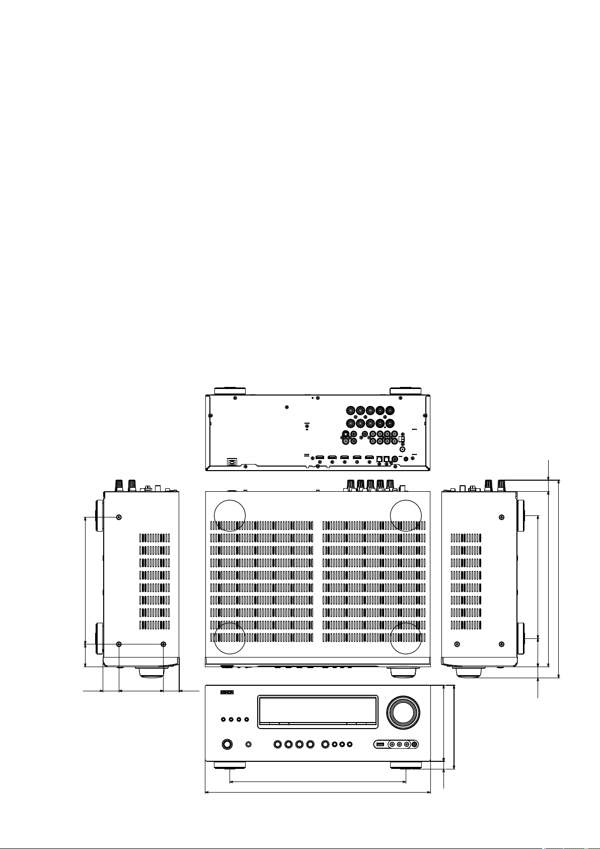
DIMENSION
Tuner section
n
[FM](Note: μV at 75 Ω, 0 dBf = 1 x 10
Receiving Range :
(E3 model)
87.5 MHz – 107.9 MHz [AM]520 kHz – 1710 kHz
[FM]
(E2,EA,E1C model)
87.5 MHz – 108.0 MHz [AM]522 kHz – 1611 kHz
[FM]
Usable Sensitivity :
[FM]1.2 μV (12.8 dBf) [AM]18 μV
50 dB Quieting Sensitivity :
[FM]MONO 2.8 μV (20.2 dBf)
S/N (IHF-A) :
[FM]MONO 70 dB
STEREO 67 dB
Total harmonic Distortion (at 1 kHz) :
[FM]MONO 0.7 %
STEREO 1.0 %
General
n
Power supply : AC 120 V, 60 Hz(E3 model)
AC 230 V, 50/60 Hz(E2 model)
AC 220 V, 50 Hz(E1C model)
Power consumption :
360 W
0.1 W (Standby)
3 W (CEC standby)
Maximum external dimensions :
435 (W) x 162 (H) x 382 (D) mm
Weight : 9.3 kg
Remote Control Unit (RC-1157)
n
Batteries : R6/AA Type (two batteries)
Maximum external dimensions : 53 (W) x 224 (H) x 28 (D) mm
Weight : 160 g (including batteries)
–15
W)
43.5 245.0
30.5
86.0
30.5
147.0
162.0
22.0
236.8
338.5
21.5 54.7
382.0
340.0
435.0
5
15.0
Page 6
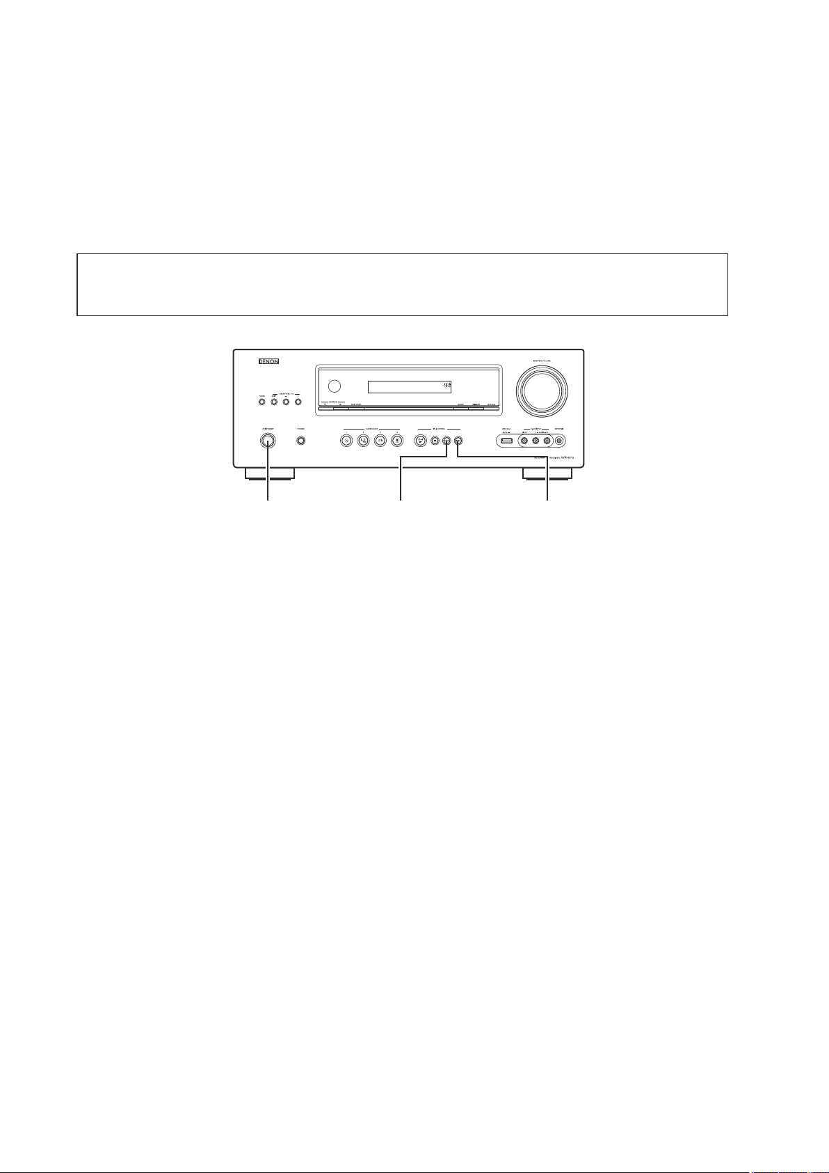
CAUTIONS IN SERVICING
Initializing AV SURROUND RECEIVER
AV SURROUND RECEIVER initialization should be performed when the μcom, peripheral parts of μcom, and Digital
P.W.B. were replaced.
1. Turn off the power pressing ON/STANDBY button.
2. Press ON/STANDBY button while simultaneously while pressing iPod system
3. Check that the entire display is ashing at intervals of about 1 second, and then release the 2 buttons.
The microprocessor will be initialized.
Note: • If step 3 fails, start over from step 1.
• All user settings will be lost and the factory setting will be recovered after the set is initialized.
So make sure to note down your setting beforehand for restoring after the initialization.
and iPod system 9 buttons.
8
ON/STANDBY iPod system 8 iPod system 9
Service Jig
When you repair the printing board, you can use the following JIG (Extension cable kit).
Please order it from Denon Ofcial Service Distributor in your region if necessary.
8U-110084S
(Refer to 35 page.)
When you update the rmware by DFW, you can use the following JIG (RS232C to internal connector conversion adapter
with 4P FFC cable kit ).
Please order to Denon Ofcial Service Distributor in your region if necessary.
8U-210100S :
(Refer to 37 page.)
EXTENSION UNIT KIT : 1 Set
:
WRITING KIT : 1 Set
6
Page 7
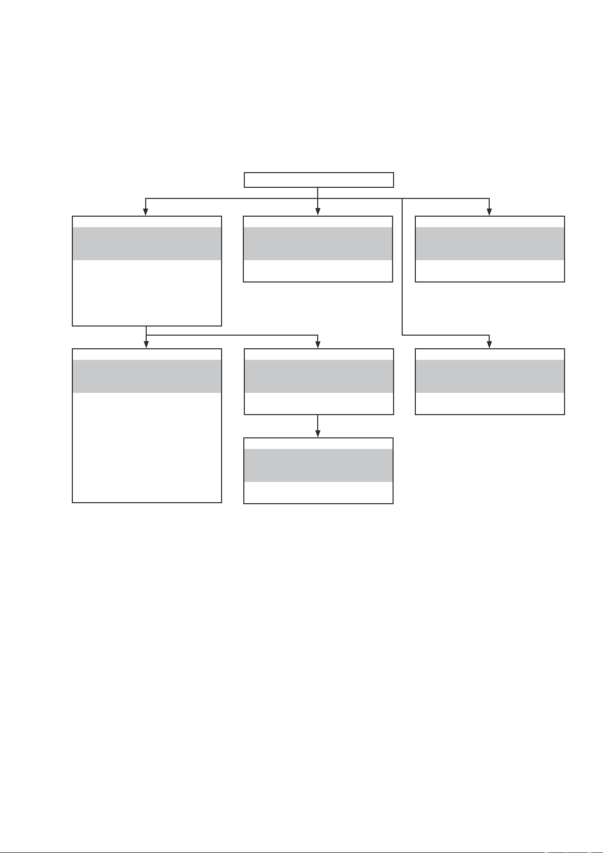
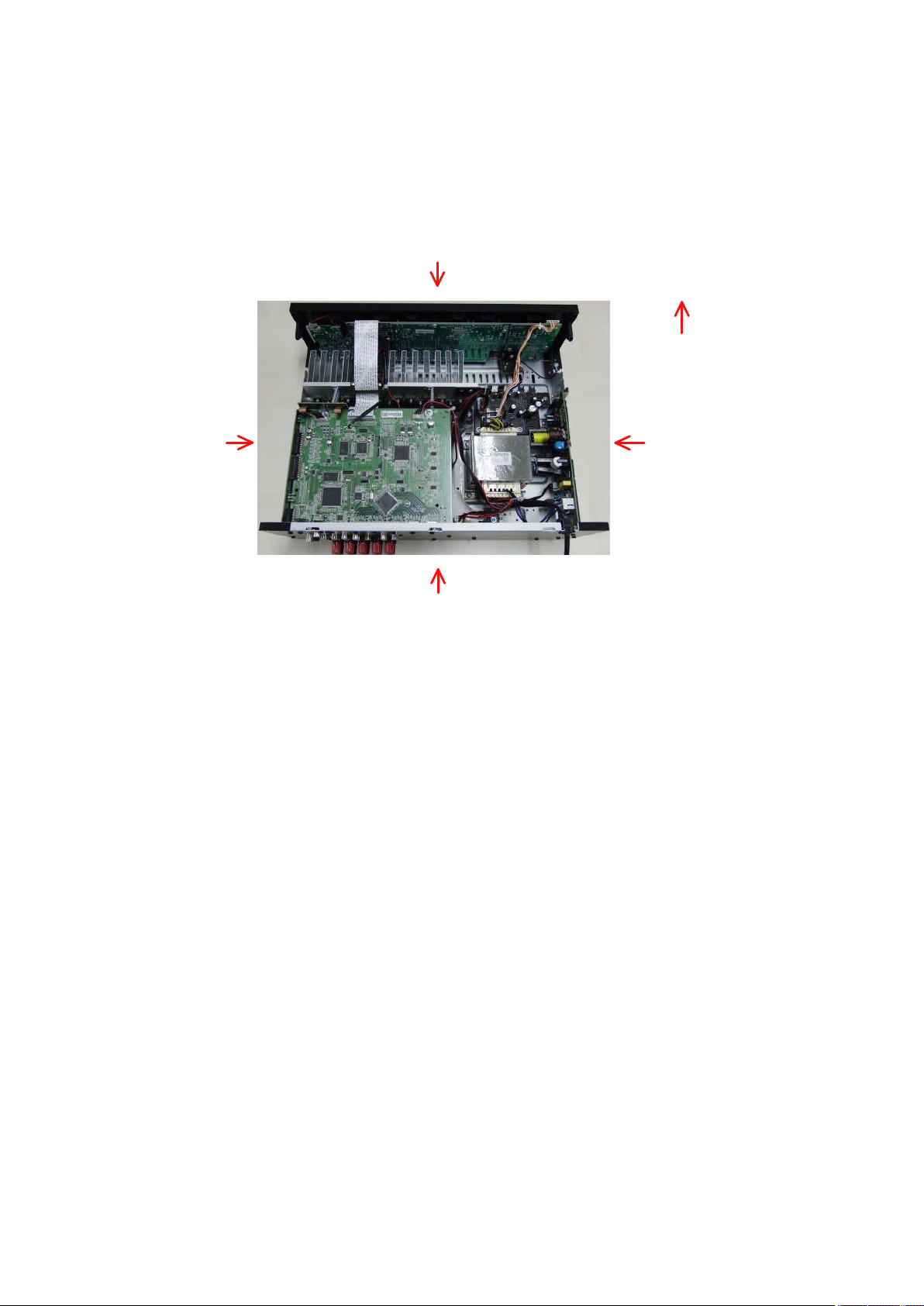
DISASSEMBLY
• Disassemble in order of the arrow in the following gure.
• In the case of the re-assembling, assemble it in order of the reverse of the following ow.
• In the case of the re-assembling, observe "attention of assembling".
• If wire bundles are untied or moved to perform adjustment or replace parts etc., be sure to rearrange them neatly as
they were originally bundled or placed afterward.
Otherwise, incorrect arrangement can be a cause of noise generation.
TOP CABINET
HDMI UNIT ASSY
Refer to "DISASSEMBLY
1. HDMI UNIT ASSY
and "EXPLODED VIEW"
CONNECTOR PCB
(Ref. No. of EXPLODED VIEW : C13)
GND CONNECT PCB
(Ref. No. of EXPLODED VIEW : C17)
DIGITAL PCB ASS'Y
(Ref. No. of EXPLODED VIEW : C12)
FRONT PANEL ASSY
Refer to "DISASSEMBLY
2. FRONT PANEL ASSY
and "EXPLODED VIEW"
HEADPHONE PCB
(Ref. No. of EXPLODED VIEW : C1)
USB PCB
(Ref. No. of EXPLODED VIEW : C2)
FRONT PCB
(Ref. No. of EXPLODED VIEW : C3)
VOLUME PCB
(Ref. No. of EXPLODED VIEW : C4)
WIRE SUPPORT PCB
(Ref. No. of EXPLODED VIEW : C7)
REGULATOR PCB
Refer to "DISASSEMBLY
5. REGULATOR PCB
and "EXPLODED VIEW"
REGULATOR PCB
(Ref. No. of EXPLODED VIEW : C6)
INPUT PCB ASSY
Refer to "DISASSEMBLY
3. INPUT PCB ASSY
and "EXPLODED VIEW"
INPUT PCB ASS'Y
(Ref. No. of EXPLODED VIEW : C11)
RADIATOR ASSY
Refer to "DISASSEMBLY
4. RADIATOR ASSY
and "EXPLODED VIEW"
MAIN PCB
(Ref. No. of EXPLODED VIEW : C10)
SMPS PCB
Refer to "DISASSEMBLY
6. PCB SMPS PCB
and "EXPLODED VIEW"
SMPS PCB
(Ref. No. of EXPLODED VIEW : C5)
TRANS POWER
Refer to "DISASSEMBLY
7. TRANS POWER
and "EXPLODED VIEW"
TRANS POWER
(Ref. No. of EXPLODED VIEW : C9)
7
Page 8
About the photos used for "descriptions of the DISASSEMBLY" section
• The shooting direction of each photograph used herein is indicated on the left side of the respective photograph as
"Shooting direction: ***".
• Refer to the diagram below about the shooting direction of each photograph.
• Photographs with no shooting direction indicated were taken from the top of the set.
• The photograph is AVR-1612E3 model.
The viewpoint of each photograph
(Shooting direction)
Shooting direction: B
View from the top
Front side
Shooting direction: DShooting direction: C
Shooting direction: A
8
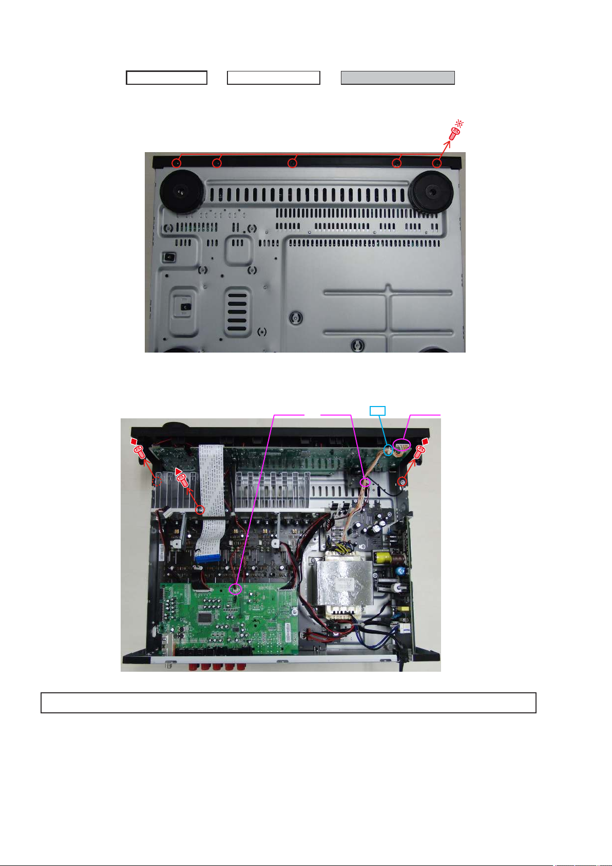
Page 9

1. HDMI UNIT ASSY
Proceeding :
(1) Disconnect the connector board.
(2) Remove the screws.
TOP CABINET
Shooting direction: C
HDMI UNIT ASSY
CONNECTOR PCB
Shooting of photograph: A
(3) Remove the screws and board.
Cut the wire clamp band, then disconnect the connector wire and the FFC cables.
FFC Cable CN151
CN252
CN341
DIGITAL PCB ASS'Y
cut
9
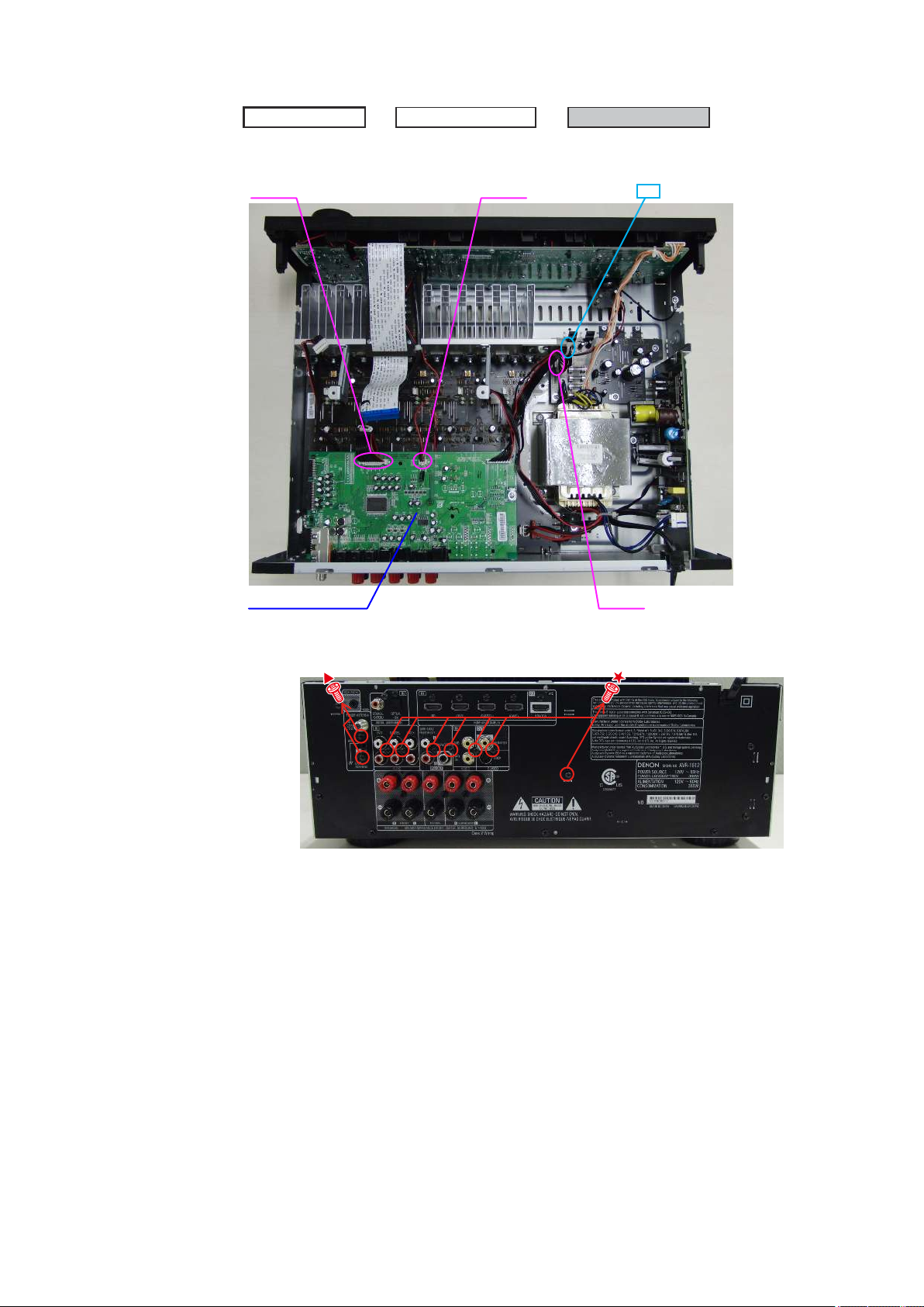
Page 10
2. FRONT PANEL ASSY
Proceeding :
(1) Remove the screws.
View from the bottom
TOP CABINET
HDMI UNIT ASSY
FRONT PANEL ASSY
(2) Cut the wire clamp band, then remove the screws.
Disconnect the connector wires.
cut
CN604CN407 CN603
Please refer to "EXPLODED VIEW" for the disassembly method of each P.W.B included in FRONT PANEL ASSY.
10
Page 11
3. INPUT PCB ASSY
Proceeding :
(1) Disconnect the connector wires and remove the INPUT PCB ASSY.
TOP CABINET
HDMI UNIT ASSY
CN407CN408
INPUT PCB ASSY
cut
INPUT PCB ASS'Y
(2) Remove the screws.
Shooting of photograph: A
CN931
11
Page 12
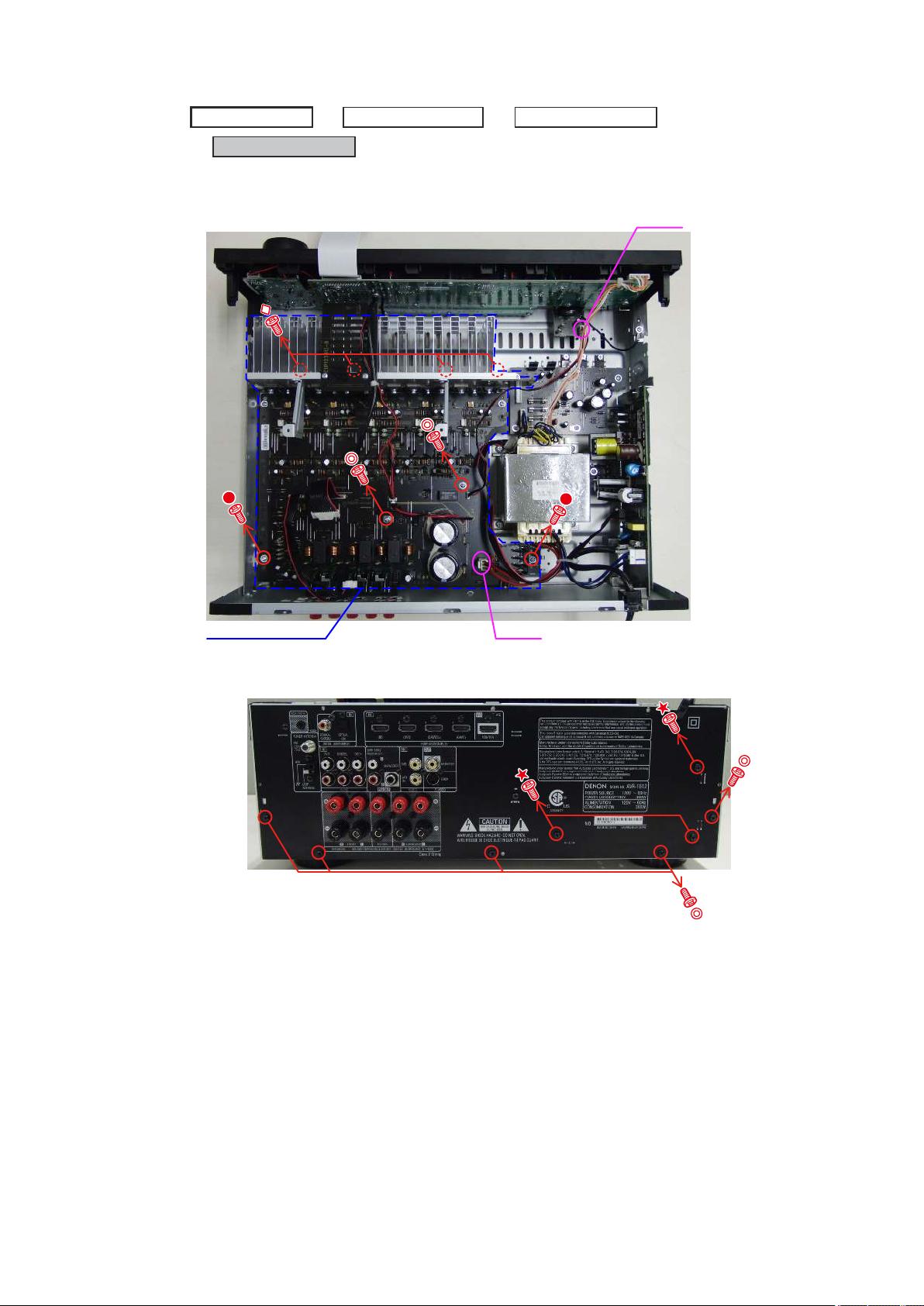
4. RADIATOR ASSY
Proceeding :
(1) Remove the screws, then disconnect the connector wires.
TOP CABINET
RADIATOR ASSY
HDMI UNIT ASSY
INPUT PCB ASSY
CN603
RADIATOR ASS'Y
(2) Remove the screws, then remove the REAR PANEL.
Shooting of photograph: A
CN703
12
Page 13
5. REGULATOR PCB
Proceeding :
Please refer to "EXPLODED VIEW" for the disassembly method of REGULATOR PCB.
TOP CABINET
REGULATOR PCB
6. SMPS PCB
Proceeding :
Please refer to "EXPLODED VIEW" for the disassembly method of SMPS PCB.
TOP CABINET
SMPS PCB
7. TRANS POWER
Proceeding :
Please refer to "EXPLODED VIEW" for the disassembly method of TRANS POWER.
TOP CABINET
TRANS POWER
13
Page 14
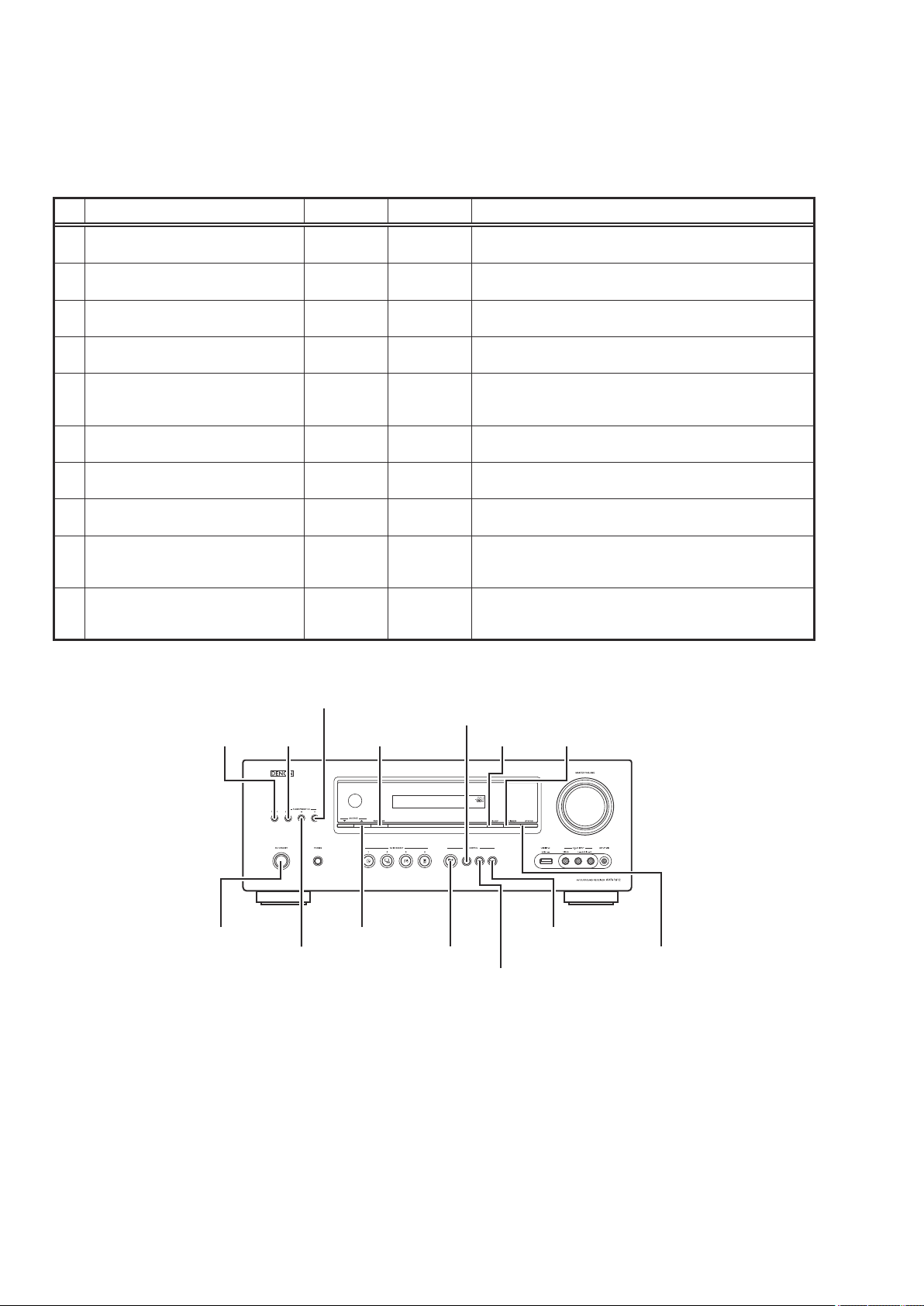
SPECIAL MODE
Special mode setting button
No.1 - 9 : Press the ON/STANDBY button to turn on the power while pressing both the button A and the button B at the same
b
No.10 : Turn on the power, then press and hold down A and B buttons for over 3 second.
b
No. Mode Button A Button B Contents
Version display
1
(μcom/DSP Error Display)
2 Displaying the protection history mode SLEEP STATUS
User Initialization mode
3
(Installer Setup settings are not initialized.)
Mode for switching tuner frequency step
4
(E2 model Only)
Mode for preventing remote control
5
acceptance
6 Panel lock mode TUNER RESTORER
Panel lock mode
7
(Master volume is not locked.)
8 Cancellation of panel lock mode
9 Diagnostic mode iPod system 2STATUS
10 Remote ID Setup mode iPod system 2STATUS
time.
DIMMER STATUS
iPod system 8iPod system 9Backup data initialization is carried out.
TUNER
PRESET CH +
iPod system
SHIFT RESTORER Operations using the main unit panel buttons are rejected.
TUNER
PRESET CH -
SOURCE dChange tuner frequency step to FM:200kHz/AM:10kHzSTEP
iPod
2
RESTORER Panel lock mode is cancelled.
Firmware versions such as Main or DSP are displayed in the FL
manager. Errors are displayed when they occur. (Refer to 15 page)
The protection history is displayed.
(Refer to 17 page)
(Installer Setup settings are not initialized.)
Operations using the remote control are rejected.
(Mode cancellation: Turn off the power and execute the same
1
button operations as when performing setup.)
Operations using the main unit panel buttons or the master volume
knob are rejected.
This mode is used for conrming the Video and Audio (signal)
paths. (Troubleshooting)
The signal paths of the set can be easily conrmed after repair.
When using multiple DENON AV receivers in the same room, make
this setting so that only the desired AV receiver operates.(Refer to 19
page)
TUNER SHIFT
ON/STANDBY
TUNER PRESET CH -
TUNER PRESET CH +
iPod system 2
RESTORER
SOURCE d
iPod 1
DIMMERSLEEP
iPod system 9
STATUS
iPod system 8
14
Page 15
1. µcom/DSP Version display mode
1.1. Operation specications
µcom/DSP version display mode:
When the set is started up in this mode, the version information is displayed.
Starting up:
Press the "ON/STANDBY" button to turn on the power while pressing the "STATUS" and "DIMMER" buttons.
Now, press the "STATUS" button to the display the 2nd item information on the FL Display.
When the version is displayed on the FL Display, the version list is also displayed on the OSD.
b
1.2. Display Order
Error information(Refer to 1.3. Error display) → q Model destination information → w Main µ-com Version
→ e Main FBL → r DSP Version → t Audio PLD Version → y OSD Version → u USB Version
→ i iPod Version (Connected only)
Model destination information :
q
FLD
A V R 1 6 1 2 E 3
FLD
A V R 1 6 1 2 E 2 / E A
FLD
A V R 1 6 1 2 E 1 C
FLD
A V R 1 6 2 2 E 1 C
Main µ-com Version :
w
FLD
(* : Main version, #: Sub version)
Main FBL :
e
FLD
DSP Version :
r
FLD
Audio PLD Version :
t
FLD
OSD Version :
y
FLD
(@: Model code, $: Brand code, x: Region code, *: version)
USB Version :
u
FLD
iPod Version :
i
FLD
M a i n : * * * * # # # #
M a i n F B L : * * . * *
D S P : * * . * *
A u d i o P L D : * * . * *
O S D : @ @ $ x * * * *
U S B : * * . * *
* i P o d D o c k : * * . * *
(ASD-1R/11R)
FLD
* D o c k : * * * * * * * * *
15
(ASD-3/51)
Page 16
1.3. Error display
See the following table for each "Error information" display and its explanation (status).
Display order is q,w,e,r,t.
Condition Status FL Display Trouble shooting
• Please check the
destination-resistors
R2031/R2032,
(
DIGITAL B'D).
• Please write the
rmware of correct
destination.
• Please check DIR
IC402, DIGITAL B'D)
(
and around circuits.
• Please check DSP
IC404, DIGITAL B'D)
(
and around circuits.
q
Firm Check
NG
w
DIR NG
e
DSP NG
r
EEPROM NG
t
Both DSP /
EEPROM OK
y
USB NG
Compared with the destination setting
on the board. This is displayed when the
model name or destination information
written into the rmware does not match.
(b)
No response from DIR
When DSP code boot is performed, the
DSP FLAG0 port does not change to "H"
even if DSP reset is executed.
Before DSP command is issued, the DSP
FLAG0 port does not change to "H".
When DSP data read is performed,
executing WRITE="L" does not result in
ACK="H".
When DSP data read is performed,
executing REQ="L" does not result in
ACK="L".
When DSP data writing is performed,
executing WRITE="H" does not result in
ACK="H".
When DSP data writing is performed,
executing REQ="L" does not result in
ACK="L".
Error occurs in EEPROM checksum.(*** is
a block address number.)
No response from USB-µcom.
F I R M E R R O R
D I R E R R O R 0 1
D S P E R R O R 0 1
D S P E R R O R 0 2
D S P E R R O R 0 3
D S P E R R O R 0 4
D S P E R R O R 0 5
D S P E R R O R 0 6
E 2 P R O M E R R * * *
(No error display, version display only)
U S B E R R O R 0 1
Status FL Display
b
When the rmware version is displayed,
▲ is displayed at the start of the rmware.
–
M a i n : * * * * * * * *
–
D S P : * * . * *
–
A u d i o P L D : * * . * *
–
O S D : * * * * * * * *
16
Page 17
2. Errors checking mode (Displaying the protection history)
2.1. Operation specications
Error mode (Displaying the protection history):
When the set is started up in this mode, the error information is displayed.
Starting up:
• Common in all the models
Press the "ON/STANDBY" button to turn on the power while pressing the "STATUS" and "SLEEP" buttons. The error
(protection history display) mode is set.
Now, press the "STATUS" button to turn on the FL display.
2.2. About the display on the FL display
When the "STATUS" button is pressed after setting the error (protection history display) mode is set, a history like the one
shown below is displayed, depending on the conditions.
(1) Normal (when there has been no protection incident)
FLD
N O P R O T E C T
(2) For ASO (when the last protection incident was ASO protection)
FLD
P R T : A S O
Cause: The line between speaker terminals is shorted, or speakers with impedance of less than the rated value.
Supplementary information: As the excess current is detected after operation of the speaker relay, a short on the
speaker terminal and the connected speaker can be identied.
If the power is turned on without correcting the abnormality, the protection function will work about 5 seconds later
and the power supply will be shut off.
(3) For DC (when the last protection incident was DC protection)
FLD
P R T : D C
Cause: DC output of the power amplier is abnormal.
If the power is turned on without correcting the abnormality, the protection function will work about 5 seconds later
and the power supply will be shut off.
(4) For THERMAL (when the last protection incident was THERMAL(A) or THERMAL(B) protection)
FLD
P R T : T H E R M A L A
FLD
P R T : T H E R M A L B
Cause: The temperature of the heat sink is excessive.
If the power is turned on without correcting the abnormality, the protection function will work about 5 seconds later
and the power supply will be shut off.
Additional causes of protection can be due to loose connections, associated components, Microprocessor, etc.
b
When the "STATUS" button is pressed again after the above protection history as shown above is displayed, the normal
display reappears.
17
Page 18

2.3. Clearing the protection history
There are two ways to clear the protection history, as described below.
(1) Start up the set in error (protection display) mode and display the error, then press and hold down the "iPod
button for 3 seconds.
FLD
P R T : D C
Press the "iPod
FLD
P R T : C L E A R
The above is displayed and the protection history is cleared.
FLD
N O P R O T E C T
(2) Initialize. (Refer to "Initializing AV SURROUND RECEIVER" 6 page.)
If you want to save a backup, perform the method in 2.3.(1) above.
b
" button for 3 seconds.
1
Warning indication by the POWER LED
If the power is turned off when a protection incident has been detected, the POWER LED (red) ashes as a warning
according to the conditions in which the protection incident occurred.
(1) ASO/DC PROTECTION : Flashes at intervals of 0.5 seconds (0.25 seconds lit, 0.25 seconds off)
(2) THERMAL (A/B) PROTECTION : Flashes at intervals of 2 seconds (1 second lit, 1 second off)
1
"
18
Page 19
3. Remote ID Setup mode
3.1. Specications
When using multiple DENON AV receivers in the same room, make this setting so that only the desired AV receiver
operates.
2.2. Setting the AV receivers
Starting up:
Press and hold both "STATUS" and "iPod system 2" buttons for over 3 second with the power turned on.
(1) When Remote ID Setup mode is started, the following is displayed.
FLD
(2) Press the "QUICK SELECT 1 - 4" button that corresponds to the number you want to set.
Button FL Display
R E M O T E I D ?
QUICK SELECT 1
QUICK SELECT 2
QUICK SELECT 3
QUICK SELECT 4
(3) Turn off the power using "ON/STANDBY" button.
(4) Turn on the power using "ON/STANDBY" button.
When Remote ID Setup mode is running, operations other than the "QUICK SELECT 1 - 4" buttons or "ON/
b
STANDBY" buttons on the main unit are not received.
R E M O T E I D 1
R E M O T E I D 2
R E M O T E I D 3
R E M O T E I D 4
2.2. Setting the Remote control unit
(1) Press the "AMP" button.
The zone mode indicator ashes twice.
(2) Press the "QUICK SELECT 1, 2, 3 or 4" button.
The zone mode indicator ashes twice.
NOTE:
If the IDs do not match, "AVAMPz" (z is the main unit's remote control ID) appears on the display when the remote
control unit is operated.
19
Page 20

Personal notes:
20
Page 21
4. DIAGNOSTIC MODE (Video/Audio (signal) path conrmation mode)
This mode is used for conrming the Video and Audio (signal) paths. (Troubleshooting)
Conrming the operation of unit can be easily done after repair.
Backup data will not be lost.
4.1. Starting diagnostic mode
Press the "iPod system 2" and "STATUS" button while simultaneously pressing those two buttons of this unit.
Q1, Q2 and Q3 are lit in FL display.
4.2. Canceling diagnostic mode
Turn off the power by pressing the ON/Standby button.
4.3. Operation
When you perform remote operation in accordance with the instructions in "Details of how to operate remote controller" *a) in the table below using the remote control unit (RC-1156 or RC-1157).
You will nd using another remote control unit with the macro functions very useful. To use the macro functions, program a macro function to output a remote control code in accordance with the steps in *b) in the table below.
4.4. Video system conrmation items
g.XX : Refer to the block diagram of the g.XXth.
Conrmation item Setting and display
Analog Video (signal) Path Display:
1
HDMI (signal) Path
2
g.1
Display:
V 0 1 D V D
V 0 1 D V D
Details of how to operate remote controller *a)
1.Press [ZONE SELECT], Select "MAIN"
2.Press [1/./]
3.Press [ZONE SELECT], Select "MAIN"
4.Press [DVD]
1.Press [ZONE SELECT], Select "MAIN"
2.Press [1/./]
3.Press [DVD]
Output sequence of remote control codes
It is useful to form a macro program. *b)
※
KEY 1/CODE1 (Main Zone)
q
Initialization
DVD (Main Zone)
w
KEY 1/CODE1 (Main Zone)
q
Initialization
DVD (Main Zone)
w
·Input : CVBS / Output : CVBS
·Input : S / Output : CVBS
·Input HDMI / Output : HDMI
(
Contents of conrmation Remarks
As the input source, you can switch from DVD to other ones.)
b
g.2
OSD FUNCTION Menu : ON
Display:
3
V 0 2 D V D
g.3
CEC FUNCTION
(Control Monitor : HDMI Monitor)
4
HDMI Audio (signal) Path
(Audio : AMP)
5
HDMI Audio (signal) Path
(Audio : TV)
6
HDMI Control : ON
Display:
g.4
g.5
g.6
V 0 3 D V D
Audio : AMP(When checking the audio output
from AMP)
Display:
V 0 5 D V D
Audio : TV(When checking the audio output
from TV)
Display:
V 0 6 D V D
1.Press [ZONE SELECT], Select "MAIN"
2.Press [2/ABC]
3.Press [ZONE SELECT], Select "MAIN"
4.Press [DVD]
5.Press [AMP]
6.Press [MENU]
1.Press [ZONE SELECT], Select "MAIN"
2.Press [3/DEF]
3.Press [DVD]
1.Press [ZONE SELECT], Select "MAIN"
2.Press [5/JKL]
3.Press [DVD]
1.Press [ZONE SELECT], Select "MAIN"
2.Press [6/MNO]
3.Press [DVD]
KEY 2/ABC (Main Zone)
q
Initialization
DVD (Main Zone)
w
GUI MENU (Main Zone)
e
KEY 3/DEF (Main Zone)
q
Initialization & CEC Control ON
DVD (Main Zone)
w
KEY 5/JKL (Main Zone)
q
Initialization & Select Audio AMP
DVD (Main Zone)
w
KEY 6/MNO (Main Zone)
q
Initialization & Audio Select TV
DVD (Main Zone)
w
·OSD Display / Output : HDMI
(b As the input source, you can switch from DVD to other ones.)
· When the power supply of a TV is put in the standby mode, make sure
that the power supply of this unit is also put in the standby mode.
(
As the input source, you can switch from DVD to other ones.)
b
·Input : HDMI (Signal of PCM, DolbyDigital or DTS) / Output : Speakers
·Input : HDMI (Signal of HD Audio) / Output : Speakers
(
As the input source, you can switch from DVD to other ones.)
b
· Input : HDMI (Signal of PCM or DolbyDigital or DTS) / Output : HDMI
(Audio output from connected TV)
(
As the input source, you can switch from DVD to other ones.)
b
21
Page 22
4.5. Audio system conrmation items
g.XX : Refer to the block diagram of the g.XXth.
Conrmation item Setting and display Details of how to operate remote controller
Analog (signal) Path Input Mode : Fixed ANALOG
SURROUND mode : DIRECT
1
g.7
Amp assign : NORMAL
Display:
A 0 1 D V D
1.Press [ZONE SELECT], Select "MAIN"
2.Press [7/PQRS]
3.Press [DVD]
Output sequence of remote control codes
It is useful to form a macro program.
b
KEY 7/PQRS (Main Zone)
q
Initialization & Amp assign NORMAL& Input Mode
Fixed ANALOG & SURROUND mode DIRECT
DVD (Main Zone)
w
Contents of conrmation Remarks
·Input : Analog / Output : Speakers (Front L/R)
(b As the input source, you can switch from DVD to other ones.)
DIGITAL (signal) Path
(MAIN)
2
g.8
HDMI (signal) Path Input Mode : Fixed HDMI
3
g.9
A/D (signal) Path
(Main Zone)
4
g.10
Input Mode : Fixed DIGITAL
Amp assign : NORMAL
Display:
A 0 2 D V D
Amp assign : NORMAL
Display:
A 0 5 D V D
Amp assign : NORMAL
SURROUND mode : Multi ch STEREO
Vol -20dB
Speaker Cong : SSSSY
(Front/Center/Surround/SourroundBack : Small, SW : Yes)
Display:
A 0 6 D V D
1.Press [ZONE SELECT], Select "MAIN"
2.Press [8/TUV]
3.Press [DVD]
1.Press [ZONE SELECT], Select "MAIN"
2.Press [MOVIE]
3.Press [DVD]
1.Press [ZONE SELECT], Select "MAIN"
2.Press [MUSIC]
3.Press [DVD]
KEY 8/TUV (Main Zone)
q
Initialization & Amp assign NORMAL& Input Mode
Fixed DIGITAL
DVD (Main Zone)
w
MOVIE Select
q
Initialization &Amp assign NORMAL & Input Mode
Fixed HDMI
DVD (Main Zone)
w
MUSIC
q
Initialization &Amp assign NORMAL &
SURROUND mode : Multi ch STEREO & Volume
-20dB
DVD (Main Zone)
w
·Input : Digital / Output : Speakers (Front L/R)
(b As the input source, you can switch from DVD to other ones.)
·Input : HDMI / Output : Speakers (Front L/R)
(b As the input source, you can switch from DVD to other ones.)
·Input : Analog / Output : Speakers (Front L/R)
·Input : Analog / Output : SW(20Hz)
(
As the input source, you can switch from DVD to other ones.)
b
22
Page 23
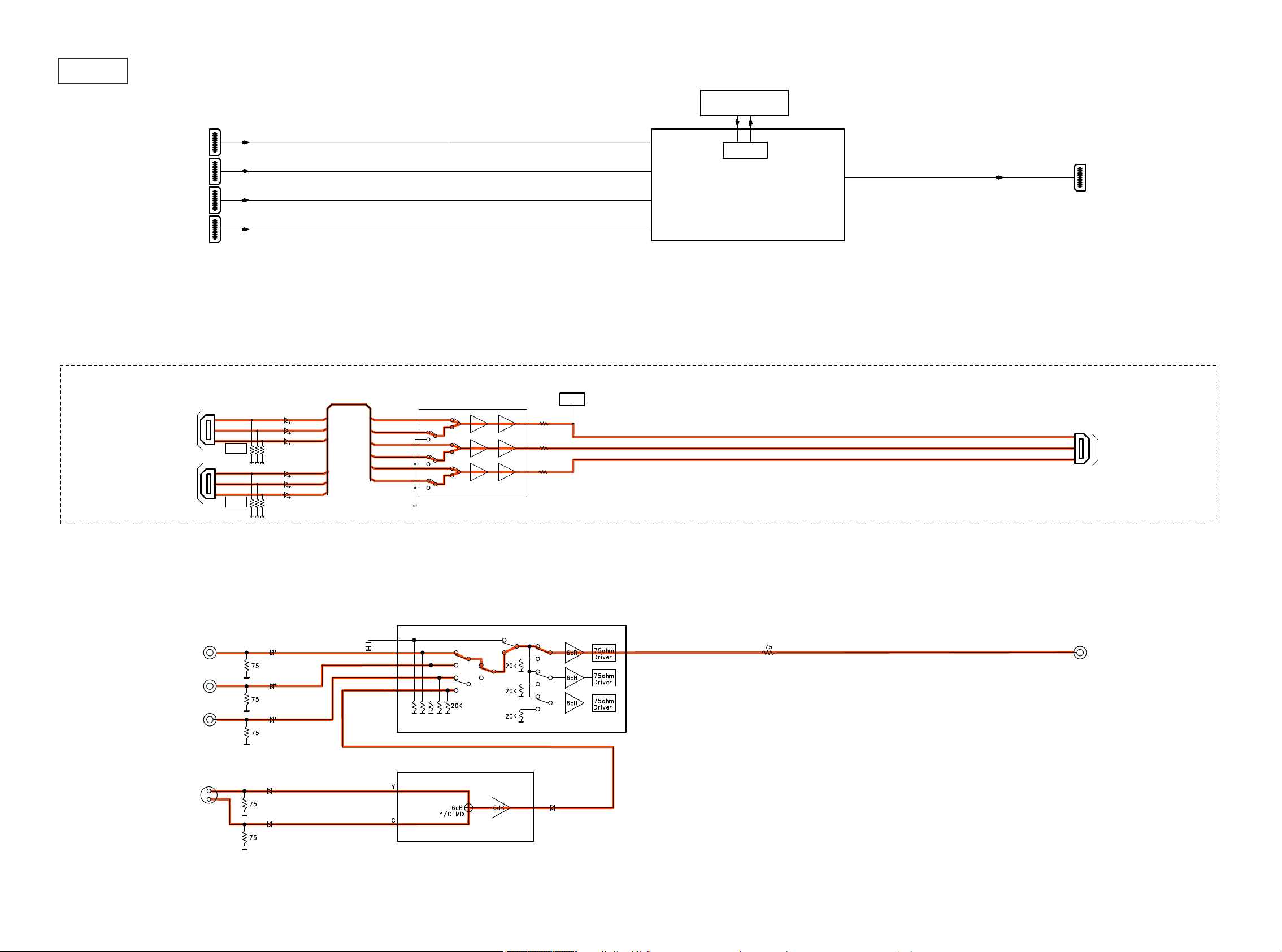
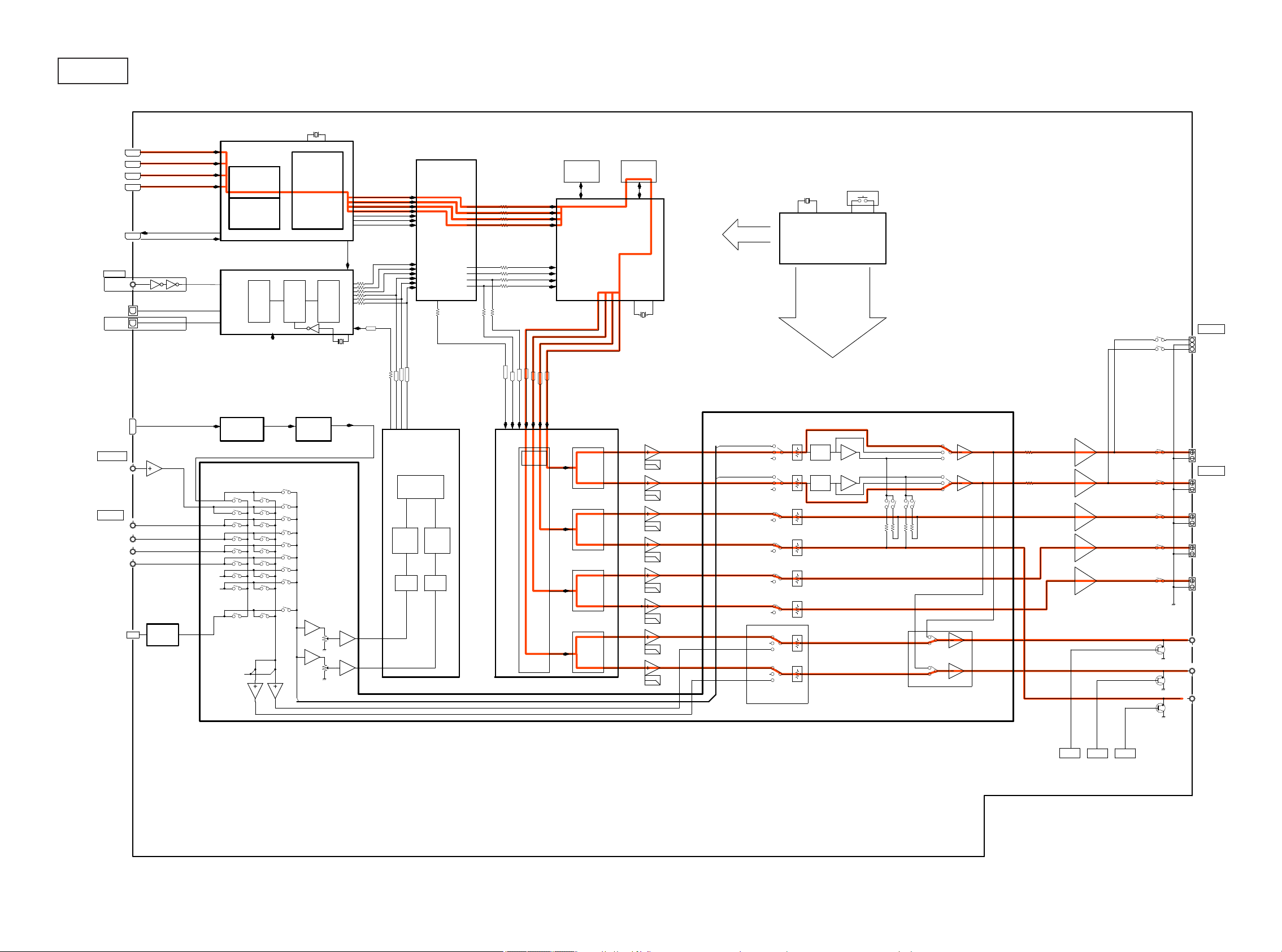
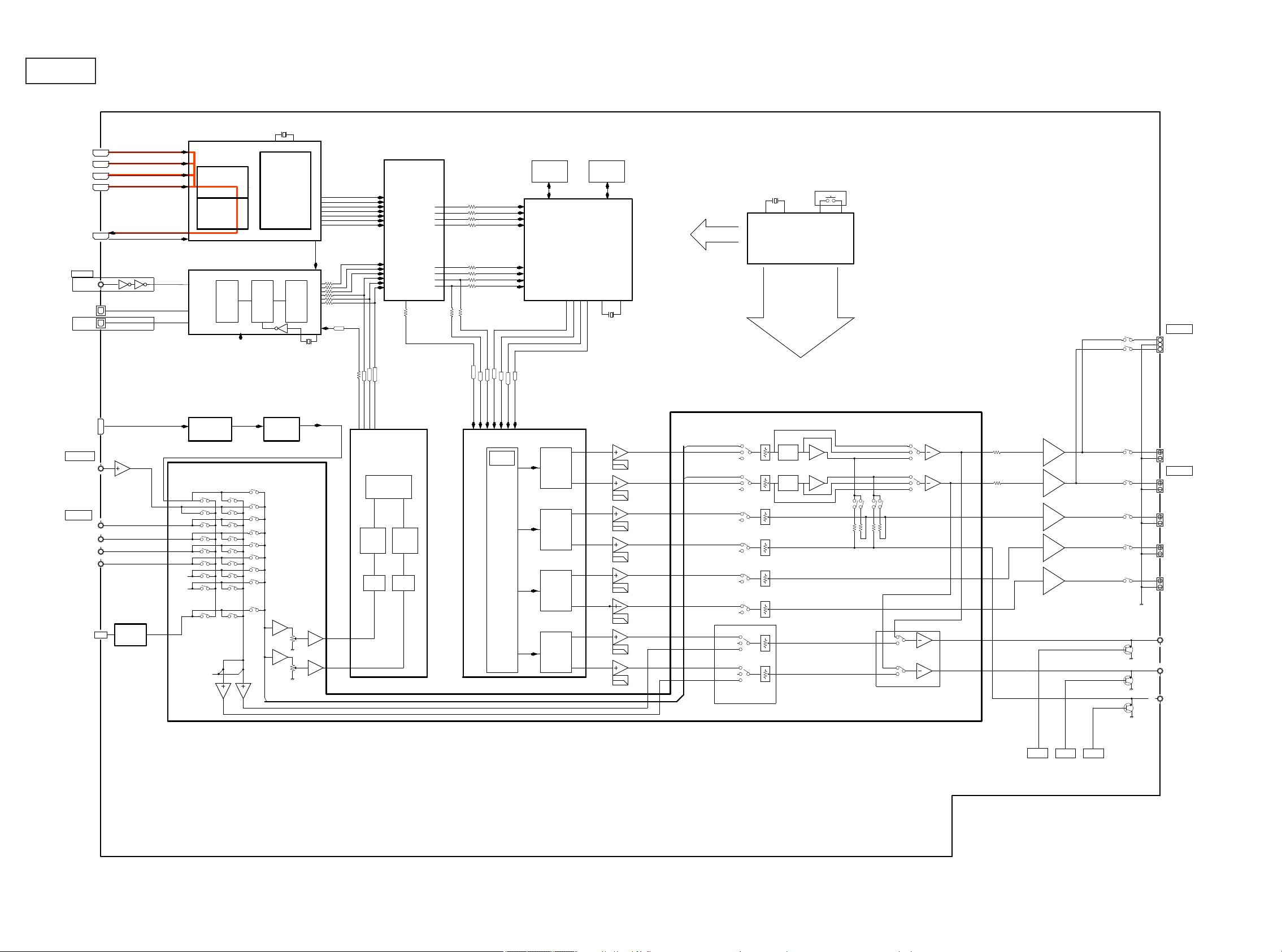
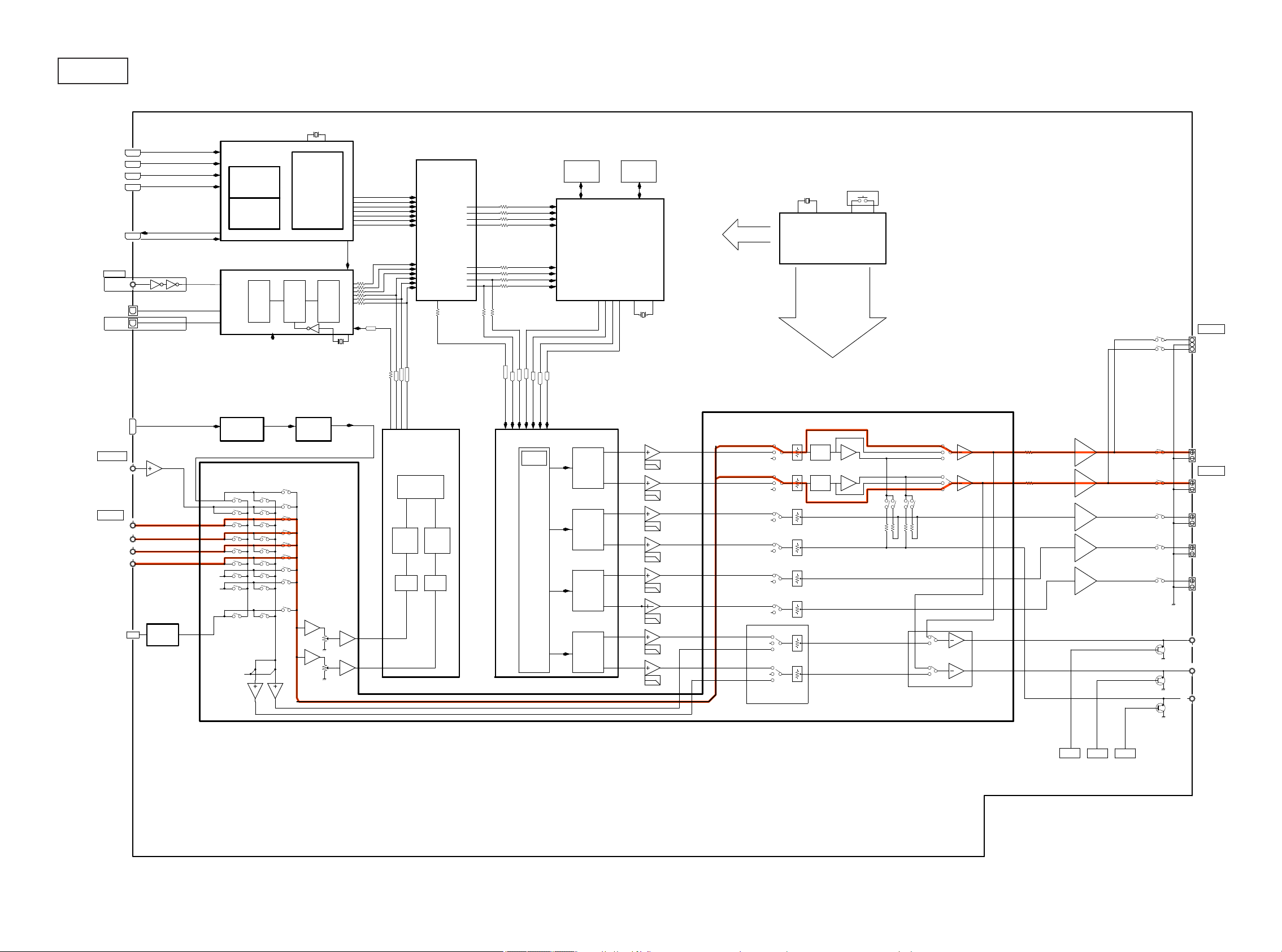
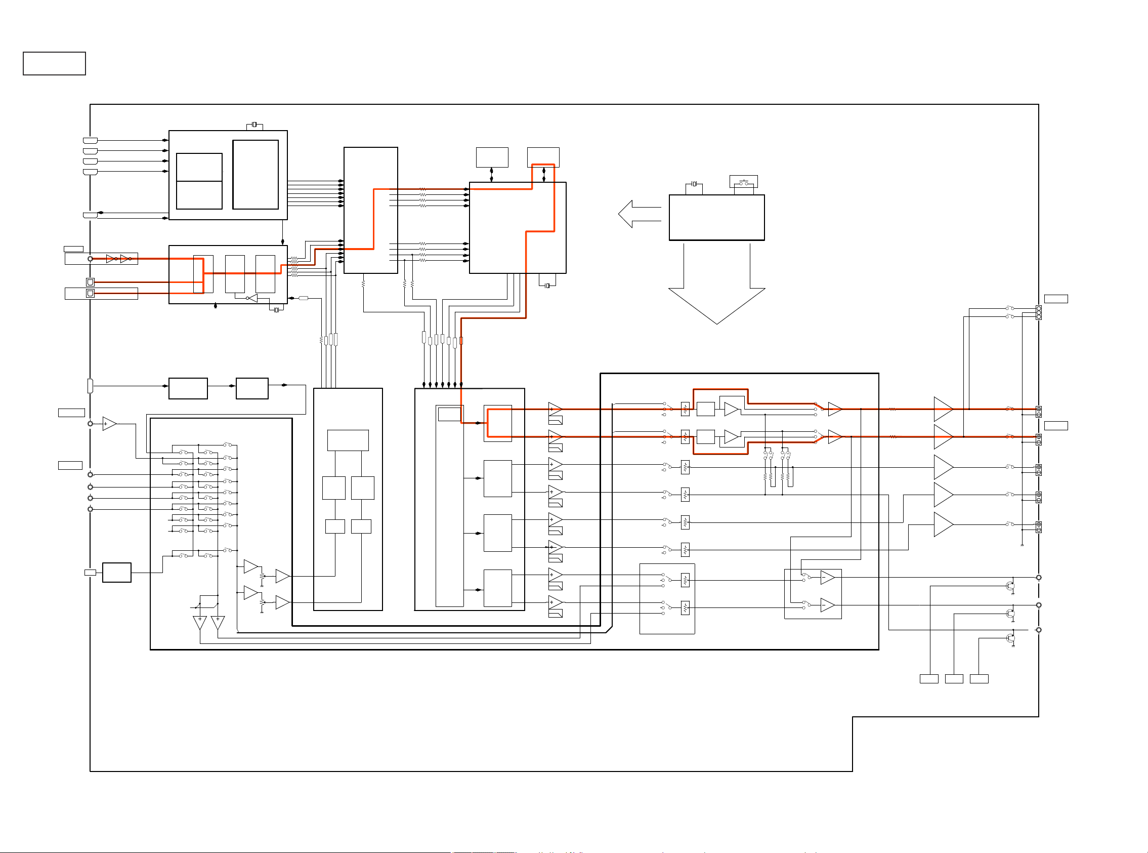
BLOCK DIAGRAM
g.1
HD M I IN
AVR1612K ONLY
COM PONENT
( D-JACK )
HD M I1
HD M I2
HD M I3
HD M I4
IN1
IN
IN2
-6dB
-6dB
COM P1-Y
COM P1-Cb
COM P1-Cr
COM P2-Y
COM P2-Cb
COM P2-Cr
COM P1-Y
COM P2-Y
COM P1-Cb
COM P2-Cb
COM P1-Cr
COM P2-Cr
IC403 (INPUT B’D)
NJM 2586M
75
6dB
75
6dB
6dB
75
VIDEO BLOCK DIAGRAM
SPI FLASH
OSD
IC9 (HDM I B’D)
ADV7623
HD M I TRANSCEIVER
DET.
75
2V
75
75
HD M I O UT
COM PONENT OUT
(D -JACK)
CVBS IN
S(Y/C) IN
DVD
SAT/CBL
V.AUX(FRON T)
DO CK
IC401 (INPUT B’D)
NJM 2595M TE1
CVBS OUT
IC401 (INPUT B’D)
M M 15111XNRE
23
Page 24
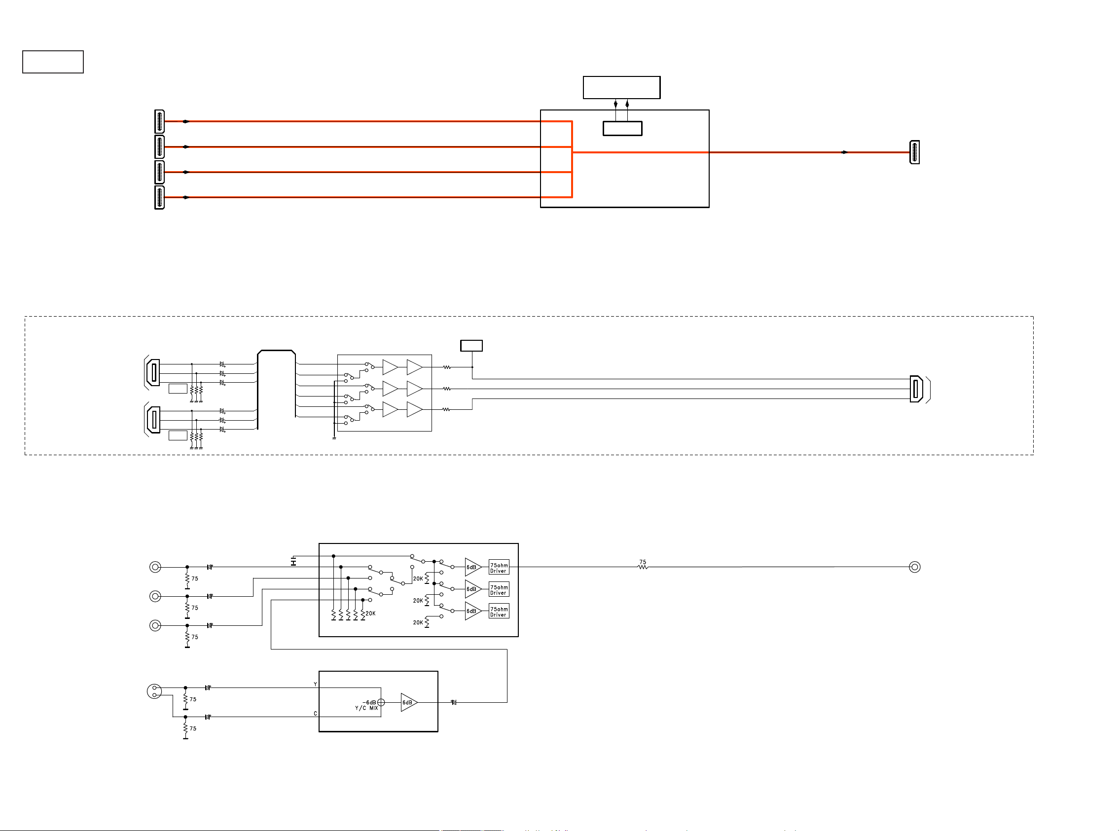
g.2
VIDEO BLOCK DIAGRAM
SPI FLASH
HDMI IN
AVR1612K ONLY
COMPONENT
( D-JACK )
HDMI1
HDMI2
HDMI3
HDMI4
IN1
IN
IN2
-6dB
-6dB
COMP1-Y
COMP1-Cb
COMP1-Cr
COMP2-Y
COMP2-Cb
COMP2-Cr
COMP1-Y
COMP2-Y
COMP1-Cb
COMP2-Cb
COMP1-Cr
COMP2-Cr
IC403 (INPUT B’D)
NJM2586M
75
6dB
75
6dB
6dB
75
2V
OSD
IC9 (HDMI B’D)
HDMI OUT
ADV7623
HDMI TRANSCEIVER
DET.
75
75
75
COMPONENT OUT
(D-JACK)
CVBS IN
V.AUX(FRONT)
S(Y/C) IN
DVD
SAT/CBL
DOCK
IC401 (INPUT B’D)
NJM2595MTE1
CVBS OUT
IC401 (INPUT B’D)
MM15111XNRE
24
Page 25
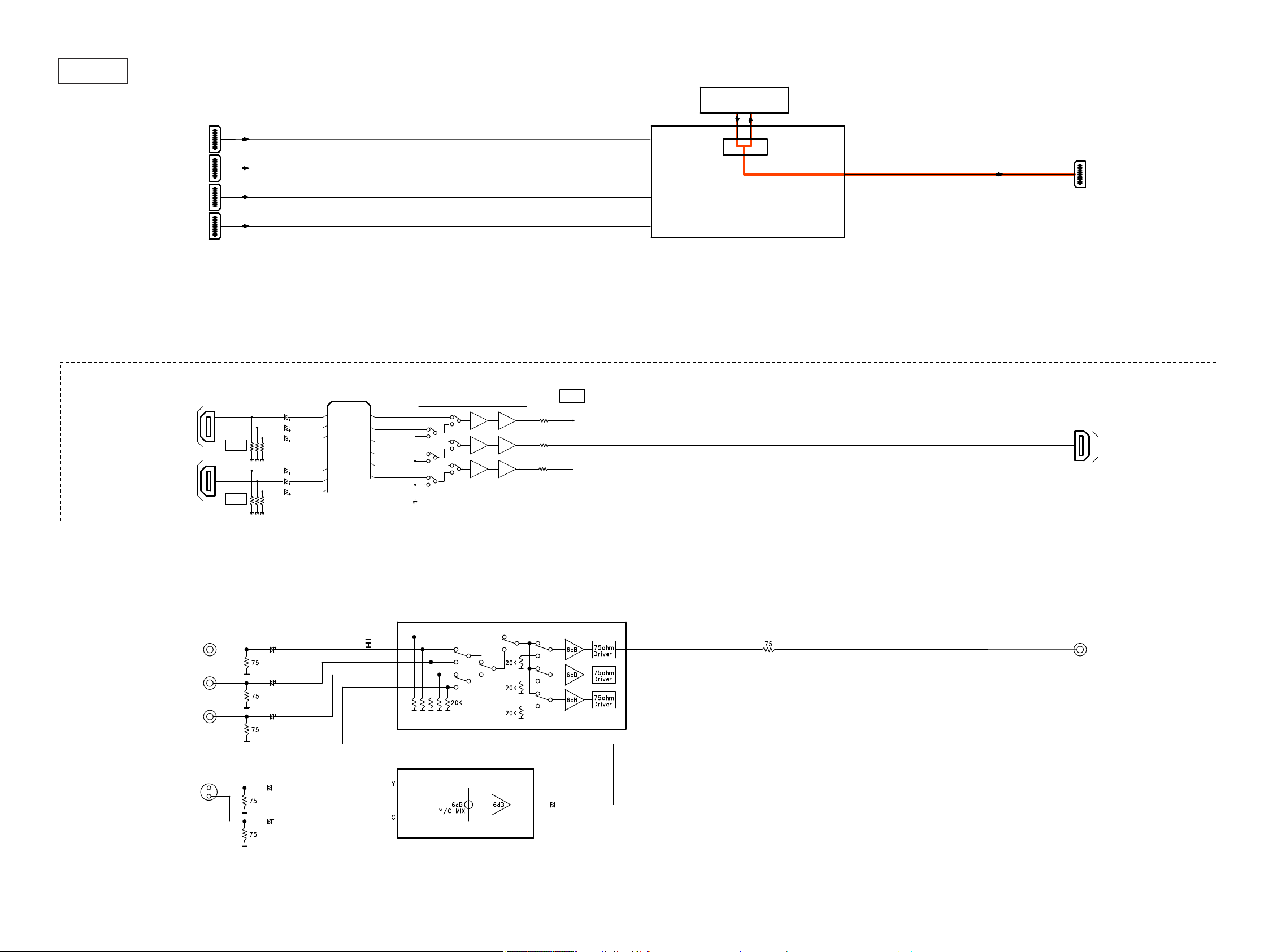
g.3
VIDEO BLOCK DIAGRAM
SPI FLASH
HDMI IN
AVR1612K ONLY
COMPONENT
( D-JACK )
HDMI1
HDMI2
HDMI3
HDMI4
IN1
IN
IN2
-6dB
-6dB
COMP1-Y
COMP1-Cb
COMP1-Cr
COMP2-Y
COMP2-Cb
COMP2-Cr
COMP1-Y
COMP2-Y
COMP1-Cb
COMP2-Cb
COMP1-Cr
COMP2-Cr
IC403 (INPUT B’D)
NJM2586M
75
6dB
75
6dB
6dB
75
2V
OSD
IC9 (HDMI B’D)
HDMI OUT
ADV7623
HDMI TRANSCEIVER
DET.
75
75
75
COMPONENT OUT
(D-JACK)
CVBS IN
V.AUX(FRONT)
S(Y/C) IN
DVD
SAT/CBL
DOCK
IC401 (INPUT B’D)
NJM2595MTE1
CVBS OUT
IC401 (INPUT B’D)
MM15111XNRE
25
Page 26
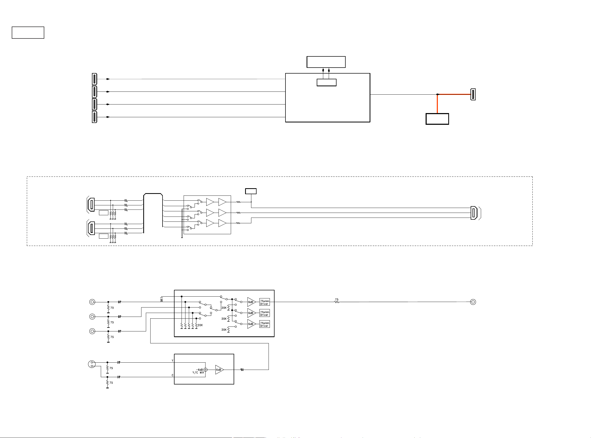
g.4
VIDEO BLOCK DIAGRAM
SPI FLASH
HDMI IN
AVR1612K ONLY
COMPONENT
( D-JACK )
HDMI1
HDMI2
HDMI3
HDMI4
IN1
IN
IN2
-6dB
-6dB
COMP1-Y
COMP1-Cb
COMP1-Cr
COMP2-Y
COMP2-Cb
COMP2-Cr
COMP1-Y
COMP2-Y
COMP1-Cb
COMP2-Cb
COMP1-Cr
COMP2-Cr
IC403 (INPUT B’D)
NJM2586M
75
6dB
75
6dB
6dB
75
OSD
IC9 (HDMI B’D)
HDMI OUT
ADV7623
HDMI TRANSCEIVER
uCOM
DET.
75
2V
75
75
COMPONENT OUT
(D-JACK)
CVBS IN
V.AUX(FRONT)
S(Y/C) IN
DVD
SAT/CBL
DOCK
IC401 (INPUT B’D)
NJM2595MTE1
CVBS OUT
IC401 (INPUT B’D)
MM15111XNRE
26
Page 27
g.5
AUDIO BLOCK DIAGRAM
HDMI IN1
HDMI IN2
HDMI IN3
HDMI IN4
HDMI OUT
DIGITAL IN
COAXIAL1
EXCULDE AVR1612JP
OPTICAL 1
OPTICAL 2
AVR1612JP ONLY
USB
AUTO SETUP
MIC
ANALOG IN
IN1
IN2
IN3
IN4
TC74VHCU04
DATA+/-
IC101(DIGITAL B’D)
ADV 7623
HDMI TRANCEIVER
HDMI RECEIVER
PROCESSOR
HDMI TRANSMITER
PROCESSOR
ARC
IC402(DIGITAL B’D)
INPUT
SELECTOR
IC301
(DIGITAL B’D)
TCC8600
USB CONTROLLER
IC404 (INPUT B’D)
R2A15218FP
INPUT SELECT & VOLUME
28.63636MHz
AUDIO
PROCESSOR
LC89058W-E DIR1
DEMO_
DULATION
&
LOCK
DETECT
IC314
(DIGITAL B’D)
AK4424ET
DAC
RXSPDIF
DATA
SELECTOR
24.576MHz
DATAAD
IC403(DIGITAL B’D)
EPM3032ATC4410
AUDIO PLD
RXI2S0
RXI2S1
RXI2S2
RXI2S3
RXMCLK
RX64FS
RXFS
SLRCK
SBCK
DATADIR1
FSDIR1
64FSDIR1
256FSDIR1
64FSDIR1
FSDIR1
256FSDIR1
IC451
(DIGITAL B’D)
AK5358BET
A/D CONVERTER
SERIAL I/O
Interface
Decimation
Decimation
FILTER
FILTER
Modulator
Modulator
DSPINDATA=>
DSP1INF
DSP1INCSW
DSP1INS
DSP1INSB
DSPIN/OUTCLK=>
DSP1IN64FS
DSP1INFS
DSP1OUT64FS
DSP1OUTFS
DAC256FS
DATASB
DATAS
DACFS
DAC64FS
AUDIO
I/F
PCM
IC406
(DIGITAL B’D)
FLASH
16MBIT
IC404 (DIGITAL B’D)
ADSP21487KSWZ3B
DIGITAL AUDIO DECODER
<= DSPOUTDATA
DATAF
DATACSW
IC441
(DIGITAL B’D)
AK4358VQ
D/A CONVERTER
DAC
DAC
DAC
IC405
(DIGITAL B’D)
SDRAM
64MBIT
21.875MHz
DATA
FUNCTION
ANA_FL
DA_FL
ANA_FR
DA_FR
DA_C
DA_SW
DA_SL
DA_SR
12MHz
KEY_MATRIX
IC2011(DIGITAL- B’D)
R5F56108VNFP
MAIN MICOM
DSP AUDIO CONT.
74LVC157.
DIR CONT.
PLD CONT
HDMI
CEC
HPD
OSD DATA
TUNER CONT
IPOD
POWER CONT
MUTE
RELAY
FL CONT
TONE
TONE
Bypass
Tone
Tone+Mix
Tone+Mix
Tone
Bypass
H/P OUT
H/P L
GND
H/P R
+
+
+ +
+
FL
SPK OUT
FR
C
SL
SR
TUNER
FM/AM
TUNER
DAC
27
DA_SBL
ZONE_L
DA_SBR
ZONE_R
ZONE2->SB ASSIGN
BI_AMP
SBL MUTE
SBR MUTE
TO MICOM
SBL
SBR
SW
SW MUTE
Page 28
g.6
AUDIO BLOCK DIAGRAM
HDMI IN1
HDMI IN2
HDMI IN3
HDMI IN4
HDMI OUT
DIGITAL IN
COAXIAL1
EXCULDE AVR1612JP
OPTICAL 1
OPTICAL 2
AVR1612JP ONLY
USB
AUTO SETUP
MIC
ANALOG IN
IN1
IN2
IN3
IN4
TC74VHCU04
DATA+/-
IC101(DIGITAL B’D)
ADV 7623
HDMI TRANCEIVER
HDMI RECEIVER
PROCESSOR
HDMI TRANSMITER
PROCESSOR
ARC
IC402(DIGITAL B’D)
INPUT
SELECTOR
IC301
(DIGITAL B’D)
TCC8600
USB CONTROLLER
IC404 (INPUT B’D)
R2A15218FP
INPUT SELECT & VOLUME
28.63636MHz
AUDIO
PROCESSOR
LC89058W-E DIR1
DEMO_
DULATION
&
LOCK
DETECT
IC314
(DIGITAL B’D)
AK4424ET
DAC
RXSPDIF
DATA
SELECTOR
24.576MHz
DATAAD
IC403(DIGITAL B’D)
EPM3032ATC4410
AUDIO PLD
RXI2S0
RXI2S1
RXI2S2
RXI2S3
RXMCLK
RX64FS
RXFS
SLRCK
SBCK
DATADIR1
FSDIR1
64FSDIR1
256FSDIR1
64FSDIR1
FSDIR1
256FSDIR1
IC451
(DIGITAL B’D)
AK5358BET
A/D CONVERTER
SERIAL I/O
Interface
Decimation
Decimation
FILTER
FILTER
Modulator
Modulator
DSPINDATA=>
DSP1INF
DSP1INCSW
DSP1INS
DSP1INSB
DSPIN/OUTCLK=>
DSP1IN64FS
DSP1INFS
DSP1OUT64FS
DSP1OUTFS
DAC256FS
DATASB
DATAS
DACFS
DAC64FS
AUDIO
I/F
PCM
IC406
(DIGITAL B’D)
FLASH
16MBIT
IC404 (DIGITAL B’D)
ADSP21487KSWZ3B
DIGITAL AUDIO DECODER
<= DSPOUTDATA
DATAF
DATACSW
IC441
(DIGITAL B’D)
AK4358VQ
D/A CONVERTER
DAC
DAC
DAC
IC405
(DIGITAL B’D)
SDRAM
64MBIT
21.875MHz
DATA
FUNCTION
ANA_FL
DA_FL
ANA_FR
DA_FR
DA_C
DA_SW
DA_SL
DA_SR
12MHz
KEY_MATRIX
IC2011(DIGITAL- B’D)
R5F56108VNFP
MAIN MICOM
DSP AUDIO CONT.
74LVC157.
DIR CONT.
PLD CONT
HDMI
CEC
HPD
OSD DATA
TUNER CONT
IPOD
POWER CONT
MUTE
RELAY
FL CONT
TONE
TONE
Bypass
Tone
Tone+Mix
Tone+Mix
Tone
Bypass
H/P OUT
H/P L
GND
H/P R
+
+
+ +
+
FL
SPK OUT
FR
C
SL
SR
TUNER
FM/AM
TUNER
DAC
28
DA_SBL
ZONE_L
DA_SBR
ZONE_R
ZONE2->SB ASSIGN
BI_AMP
SBL MUTE
SBR MUTE
TO MICOM
SBL
SBR
SW
SW MUTE
Page 29
g.7
AUDIO BLOCK DIAGRAM
HDMI IN1
HDMI IN2
HDMI IN3
HDMI IN4
HDMI OUT
DIGITAL IN
COAXIAL1
EXCULDE AVR1612JP
OPTICAL 1
OPTICAL 2
AVR1612JP ONLY
USB
AUTO SETUP
MIC
ANALOG IN
IN1
IN2
IN3
IN4
TC74VHCU04
DATA+/-
IC101(DIGITAL B’D)
ADV 7623
HDMI TRANCEIVER
HDMI RECEIVER
PROCESSOR
HDMI TRANSMITER
PROCESSOR
ARC
IC402(DIGITAL B’D)
INPUT
SELECTOR
IC301
(DIGITAL B’D)
TCC8600
USB CONTROLLER
IC404 (INPUT B’D)
R2A15218FP
INPUT SELECT & VOLUME
28.63636MHz
AUDIO
PROCESSOR
LC89058W-E DIR1
DEMO_
DULATION
&
LOCK
DETECT
IC314
(DIGITAL B’D)
AK4424ET
DAC
RXSPDIF
DATA
SELECTOR
24.576MHz
DATAAD
IC403(DIGITAL B’D)
EPM3032ATC4410
AUDIO PLD
RXI2S0
RXI2S1
RXI2S2
RXI2S3
RXMCLK
RX64FS
RXFS
SLRCK
SBCK
DATADIR1
FSDIR1
64FSDIR1
256FSDIR1
64FSDIR1
FSDIR1
256FSDIR1
IC451
(DIGITAL B’D)
AK5358BET
A/D CONVERTER
SERIAL I/O
Interface
Decimation
Decimation
FILTER
FILTER
Modulator
Modulator
DSPINDATA=>
DSP1INF
DSP1INCSW
DSP1INS
DSP1INSB
DSPIN/OUTCLK=>
DSP1IN64FS
DSP1INFS
DSP1OUT64FS
DSP1OUTFS
DAC256FS
DATASB
DATAS
DACFS
DAC64FS
AUDIO
I/F
PCM
IC406
(DIGITAL B’D)
FLASH
16MBIT
IC404 (DIGITAL B’D)
ADSP21487KSWZ3B
DIGITAL AUDIO DECODER
<= DSPOUTDATA
DATAF
DATACSW
IC441
(DIGITAL B’D)
AK4358VQ
D/A CONVERTER
DAC
DAC
DAC
IC405
(DIGITAL B’D)
SDRAM
64MBIT
21.875MHz
DATA
FUNCTION
ANA_FL
DA_FL
ANA_FR
DA_FR
DA_C
DA_SW
DA_SL
DA_SR
12MHz
KEY_MATRIX
IC2011(DIGITAL- B’D)
R5F56108VNFP
MAIN MICOM
DSP AUDIO CONT.
74LVC157.
DIR CONT.
PLD CONT
HDMI
CEC
HPD
OSD DATA
TUNER CONT
IPOD
POWER CONT
MUTE
RELAY
FL CONT
TONE
TONE
Bypass
Tone
Tone+Mix
Tone+Mix
Tone
Bypass
H/P OUT
H/P L
GND
H/P R
+
+
+ +
+
FL
SPK OUT
FR
C
SL
SR
TUNER
FM/AM
TUNER
DAC
29
DA_SBL
ZONE_L
DA_SBR
ZONE_R
ZONE2->SB ASSIGN
BI_AMP
SBL MUTE
SBR MUTE
TO MICOM
SBL
SBR
SW
SW MUTE
Page 30
g.830g.9
AUDIO BLOCK DIAGRAM
HDMI IN1
HDMI IN2
HDMI IN3
HDMI IN4
HDMI OUT
DIGITAL IN
COAXIAL1
EXCULDE AVR1612JP
OPTICAL 1
OPTICAL 2
AVR1612JP ONLY
USB
AUTO SETUP
MIC
ANALOG IN
IN1
IN2
IN3
IN4
TC74VHCU04
DATA+/-
IC101(DIGITAL B’D)
ADV 7623
HDMI TRANCEIVER
HDMI RECEIVER
PROCESSOR
HDMI TRANSMITER
PROCESSOR
ARC
IC402(DIGITAL B’D)
INPUT
SELECTOR
IC301
(DIGITAL B’D)
TCC8600
USB CONTROLLER
IC404 (INPUT B’D)
R2A15218FP
INPUT SELECT & VOLUME
28.63636MHz
AUDIO
PROCESSOR
LC89058W-E DIR1
DEMO_
DULATION
&
LOCK
DETECT
IC314
(DIGITAL B’D)
AK4424ET
DAC
RXSPDIF
DATA
SELECTOR
24.576MHz
DATAAD
IC403(DIGITAL B’D)
EPM3032ATC4410
AUDIO PLD
RXI2S0
RXI2S1
RXI2S2
RXI2S3
RXMCLK
RX64FS
RXFS
SLRCK
SBCK
DATADIR1
FSDIR1
64FSDIR1
256FSDIR1
64FSDIR1
FSDIR1
256FSDIR1
IC451
(DIGITAL B’D)
AK5358BET
A/D CONVERTER
SERIAL I/O
Interface
Decimation
Decimation
FILTER
FILTER
DSPINDATA=>
DSP1INF
DSP1INCSW
DSP1INS
DSP1INSB
DSPIN/OUTCLK=>
DSP1IN64FS
DSP1INFS
DSP1OUT64FS
DSP1OUTFS
DAC256FS
DATASB
DATAS
DACFS
DAC64FS
AUDIO
I/F
PCM
IC406
(DIGITAL B’D)
FLASH
16MBIT
IC404 (DIGITAL B’D)
ADSP21487KSWZ3B
DIGITAL AUDIO DECODER
<= DSPOUTDATA
DATAF
DATACSW
IC441
(DIGITAL B’D)
AK4358VQ
D/A CONVERTER
DAC
DAC
IC405
(DIGITAL B’D)
SDRAM
64MBIT
21.875MHz
DATA
FUNCTION
ANA_FL
DA_FL
ANA_FR
DA_FR
DA_C
DA_SW
12MHz
KEY_MATRIX
IC2011(DIGITAL- B’D)
R5F56108VNFP
MAIN MICOM
DSP AUDIO CONT.
74LVC157.
DIR CONT.
PLD CONT
HDMI
CEC
HPD
OSD DATA
TUNER CONT
IPOD
POWER CONT
MUTE
RELAY
FL CONT
TONE
TONE
Bypass
Tone
Tone+Mix
Tone+Mix
Tone
Bypass
H/P OUT
H/P L
GND
H/P R
+
+
+ +
FL
SPK OUT
FR
C
SL
DA_SL
Modulator
Modulator
DAC
+
SR
DA_SR
TUNER
FM/AM
TUNER
DAC
DA_SBL
ZONE_L
DA_SBR
ZONE_R
ZONE2->SB ASSIGN
BI_AMP
SBL MUTE
SBR MUTE
TO MICOM
SBL
SBR
SW
SW MUTE
Page 31

AUDIO BLOCK DIAGRAM
HDMI IN1
HDMI IN2
HDMI IN3
HDMI IN4
HDMI OUT
DIGITAL IN
COAXIAL1
EXCULDE AVR1612JP
OPTICAL 1
OPTICAL 2
AVR1612JP ONLY
USB
AUTO SETUP
MIC
ANALOG IN
IN1
IN2
IN3
IN4
TC74VHCU04
DATA+/-
IC101(DIGITAL B’D)
ADV 7623
HDMI TRANCEIVER
HDMI RECEIVER
PROCESSOR
HDMI TRANSMITER
PROCESSOR
ARC
IC402(DIGITAL B’D)
INPUT
SELECTOR
IC301
(DIGITAL B’D)
TCC8600
USB CONTROLLER
IC404 (INPUT B’D)
R2A15218FP
INPUT SELECT & VOLUME
28.63636MHz
AUDIO
PROCESSOR
LC89058W-E DIR1
DEMO_
DULATION
&
LOCK
DETECT
IC314
(DIGITAL B’D)
AK4424ET
DAC
RXSPDIF
DATA
SELECTOR
24.576MHz
DATAAD
IC403(DIGITAL B’D)
EPM3032ATC4410
AUDIO PLD
RXI2S0
RXI2S1
RXI2S2
RXI2S3
RXMCLK
RX64FS
RXFS
SLRCK
SBCK
DATADIR1
FSDIR1
64FSDIR1
256FSDIR1
64FSDIR1
FSDIR1
256FSDIR1
IC451
(DIGITAL B’D)
AK5358BET
A/D CONVERTER
SERIAL I/O
Interface
Decimation
Decimation
FILTER
FILTER
DSPINDATA=>
DSP1INF
DSP1INCSW
DSP1INS
DSP1INSB
DSPIN/OUTCLK=>
DSP1IN64FS
DSP1INFS
DSP1OUT64FS
DSP1OUTFS
DAC256FS
DATASB
DATAS
DACFS
DAC64FS
AUDIO
I/F
PCM
IC406
(DIGITAL B’D)
FLASH
16MBIT
IC404 (DIGITAL B’D)
ADSP21487KSWZ3B
DIGITAL AUDIO DECODER
<= DSPOUTDATA
DATAF
DATACSW
IC441
(DIGITAL B’D)
AK4358VQ
D/A CONVERTER
DAC
DAC
IC405
(DIGITAL B’D)
SDRAM
64MBIT
21.875MHz
DATA
FUNCTION
ANA_FL
DA_FL
ANA_FR
DA_FR
DA_C
DA_SW
12MHz
KEY_MATRIX
IC2011(DIGITAL- B’D)
R5F56108VNFP
MAIN MICOM
DSP AUDIO CONT.
74LVC157.
DIR CONT.
PLD CONT
HDMI
CEC
HPD
OSD DATA
TUNER CONT
IPOD
POWER CONT
MUTE
RELAY
FL CONT
TONE
TONE
Bypass
Tone
Tone+Mix
Tone+Mix
Tone
Bypass
H/P OUT
H/P L
GND
H/P R
+
+
+ +
FL
SPK OUT
FR
C
SL
DA_SL
Modulator
Modulator
DAC
+
SR
DA_SR
TUNER
FM/AM
TUNER
DAC
31
DA_SBL
ZONE_L
DA_SBR
ZONE_R
ZONE2->SB ASSIGN
BI_AMP
SBL MUTE
SBR MUTE
TO MICOM
SBL
SBR
SW
SW MUTE
Page 32

g.10
AUDIO BLOCK DIAGRAM
HDMI IN1
HDMI IN2
HDMI IN3
HDMI IN4
HDMI OUT
DIGITAL IN
COAXIAL1
EXCULDE AVR1612JP
OPTICAL 1
OPTICAL 2
AVR1612JP ONLY
USB
AUTO SETUP
MIC
ANALOG IN
IN1
IN2
IN3
IN4
TC74VHCU04
DATA+/-
IC101(DIGITAL B’D)
ADV 7623
HDMI TRANCEIVER
HDMI RECEIVER
PROCESSOR
HDMI TRANSMITER
PROCESSOR
ARC
IC402(DIGITAL B’D)
INPUT
SELECTOR
IC301
(DIGITAL B’D)
TCC8600
USB CONTROLLER
IC404 (INPUT B’D)
R2A15218FP
INPUT SELECT & VOLUME
28.63636MHz
AUDIO
PROCESSOR
LC89058W-E DIR1
DEMO_
DULATION
&
LOCK
DETECT
IC314
(DIGITAL B’D)
AK4424ET
DAC
RXSPDIF
DATA
SELECTOR
24.576MHz
DATAAD
IC403(DIGITAL B’D)
EPM3032ATC4410
AUDIO PLD
RXI2S0
RXI2S1
RXI2S2
RXI2S3
RXMCLK
RX64FS
RXFS
SLRCK
SBCK
DATADIR1
FSDIR1
64FSDIR1
256FSDIR1
64FSDIR1
FSDIR1
256FSDIR1
IC451
(DIGITAL B’D)
AK5358BET
A/D CONVERTER
SERIAL I/O
Interface
Decimation
Decimation
FILTER
FILTER
Modulator
Modulator
DSPINDATA=>
DSP1INF
DSP1INCSW
DSP1INS
DSP1INSB
DSPIN/OUTCLK=>
DSP1IN64FS
DSP1INFS
DSP1OUT64FS
DSP1OUTFS
DAC256FS
DATASB
DATAS
DACFS
DAC64FS
AUDIO
I/F
PCM
IC406
(DIGITAL B’D)
FLASH
16MBIT
IC404 (DIGITAL B’D)
ADSP21487KSWZ3B
DIGITAL AUDIO DECODER
<= DSPOUTDATA
DATAF
DATACSW
IC441
(DIGITAL B’D)
AK4358VQ
D/A CONVERTER
DAC
DAC
DAC
IC405
(DIGITAL B’D)
SDRAM
64MBIT
21.875MHz
DATA
FUNCTION
ANA_FL
DA_FL
ANA_FR
DA_FR
DA_C
DA_SW
DA_SL
DA_SR
12MHz
KEY_MATRIX
IC2011(DIGITAL- B’D)
R5F56108VNFP
MAIN MICOM
DSP AUDIO CONT.
74LVC157.
DIR CONT.
PLD CONT
HDMI
CEC
HPD
OSD DATA
TUNER CONT
IPOD
POWER CONT
MUTE
RELAY
FL CONT
TONE
TONE
Bypass
Tone
Tone+Mix
Tone+Mix
Tone
Bypass
H/P OUT
H/P L
GND
H/P R
+
+
+ +
+
FL
SPK OUT
FR
C
SL
SR
TUNER
FM/AM
TUNER
DAC
32
DA_SBL
ZONE_L
DA_SBR
ZONE_R
ZONE2->SB ASSIGN
BI_AMP
SBL MUTE
SBR MUTE
TO MICOM
SBL
SBR
SW
SW MUTE
Page 33

VCC BLOCK DIAGRAM
!
MAIN+B
!
AC CORD
RELAY
!
S1(AMP+B,-B)
S2(+12 V,-1 2V)
MAIN TRANS
S3(VID EO)
S4(FL+ Vdis p)
2
4
1
3
MAIN B’D
MAIN-B
60mA
VOLUM E IC
NJM78 12FA
NJM79 12FA
REGULATOR B’D
MTZ7.5B
KIA7805 BPI
MTZ7.5B
KIA7805 BPI
210mA
112mA
50mA
57mA
(R2A152 18FP )
60mA
A+12V
(AZ4580,SPK RELAY)
120mA
90mA
DA+5V
(AK4358V Q,AK5358 ,AK4424 )
85mA 27mA
40mA
TUNER +5V
A-12V
VOLUM E IC
(R2A152 18FP )
V+5V
(NJM258 6,NJM25 95)
35mA 22mA
INPUT B’D
KIA7905 PI
68mA
V-5V
Vdisp(+ 37V)
!
SMPS B’D
FRONT B’D
163mA
FILAMEN T AC
S5(FILAMENT)
FILAMEN T AC
SWM5V/ LEVEL_C HG
1.5mA
+5.2V
EX3AV(+3.3V )
D
G
S
12
3 4
MAIN PWR ON
EX3AV(+1.8V )
EX3AV(+1.8V )
EX3AV(+1.1V )
OPEN
DIGITAL B’D
PQ018ENA1ZPH
715.202 mA
1304.62 mA
(SN74LV C244APWR ,TC74VH CT08)
1000mA
339mA
214mA
3mA
982mA
1.5mA
/VBU S
D5V
+5VH /HD MI
DA3.3V /DIR ,DSP
(ADSP2148 7,W9864 G6JH,EPM 3032,L C8905 8,TC74V HCU04 ,MX29L V160)
0.2mA 400mA 225 mA 60 mA 0.002m A
+3V3 H/HD MI
(ADV7623 ,MX25L 3206E)
314mA 25mA
NET3.3V /USB
(TCC8600 ,IS42S16 400F,M X29LV 160D)
4mA 180mA
NET1.8V /USB
(TCC8600 )
3mA
+1V8 H/HD MI
(ADV7623 )
982mA
DA1.1V /DSP
(ADSP2148 7)
1304.62 mA
30mA
30mA
33
PQ033DNA1 ZPH
1.5mA
55mA
SWM3.3V /LEV EL_CHG
(TC74VHC 08)
1.5mA
MCU_3 V3/M ICOM
(R5F561 08VNF P,M24C 32)
50mA 5mA
Page 34

Personal notes: Personal notes:
34
Page 35

JIG FOR SERVICING
When you repair the printing board, you can use the following JIG (Extension cable kit).
Please order it from DENON Ofcial Service. Distributor in your region if necessary.
NOTE
: The incorrect connection with in the JIG (EXTENSION UNIT KIT) may cause damage.
8U-110084S : EXTENSION UNIT KIT : 1 Set
• Connection of PCB HDMI JIG
-Preparation-
8U-110084S : EXTENSION UNIT KIT : 1 Set
Insulation sheet (Do not supply it) : 1 sheet
Ground lead (Do not supply it) : 1 pc
-Procedures-
(1) Remove the screws.
(2) Disconnect the connector board.
Board to board
CN150
CN151FFC cable
PCB DIGITAL
35
Page 36

(3) Detach PCB DIGITAL is detached from the chassis, and turn it over.
Please put an insulation sheet that is larger than PCB DIGITAL under PCB.
Connect the ground point of PCB to the chassis with a ground lead or the like.
b
PCB DIGITAL
(4) Connect the six extension jig cables.
Ground lead
Insulation sheet
1
2
3
Connection table of Board to Board
No. Pin Ref. No. PCB Ref. No. PCB
q
w
e
21 pin CN254 CONNECTOR
23 pin CN256 CONNECTOR
13 pin CN258 CONNECTOR
CN254 DIGITAL
CN403 DIGITAL
CN253 DIGITAL
PCB DIGITAL
36
Page 37

WHEN THE MICROPROCESSOR IS REPLACED WITH A NEW ONE
When the U-PRO (Microprocessor) or the Flash ROM is replaced, conrm the following.
PWB Name Ref. No. Description
DIGITAL IC201 R5F56108VNFP B SOFTWARE: Main
DIGITAL IC406 MX29LV160DBTI-70G B SOFTWARE: DSP ROM
DIGITAL IC403 EPM3032A-TC44 B SOFTWARE: AUDIO PLD
DIGITAL IC102 MX25L3206EM2I-12G B SOFTWARE: OSD ROM; E3,JP model
DIGITAL IC102 MX25L6406EM2I-12G B SOFTWARE: OSD ROM;
After
replaced
Remark
E2,E1C model
After replacing
A
: Mask ROM (With software). No need for write-in of software to the microprocessor.
B : Flash ROM (With software). Usually, no need for write-in of software. But, when the software was updated, you should
write the new software on the microprocessor or ash ROM. Please check the software version.
C
: Empty Flash ROM (Without software). You should write the software on the microprocessor or ash ROM.
Refer to "Update procedure" or "writing procedure", when you write the software.
PROCEDURE FOR UPGRADING THE VERSION OF THE FIRMWARE
1. How to update by DFW
1.1. Preparations before starting the operation
(1) Personal Computer (Installed "DFW_0048_AVR1612(Rev.1.1.1).exe".
(2) RS-232 cable (9P (Male ), Straight).
(3) 8U-210100 Writing Kit.
1.2. Connection of AV receiver
(1) Conrm the power on/off switch of the AV receiver is turning off.
(2) Connect the update terminal of AV receiver with the "Writing Kit".
(3) Connect the RS-232C cable from PC with the "Writing Kit".
4P FFC Cable
This side is contacts of
flexible card cable.
Writing Kit
S706-709 : No Preference
S709
S708
S707
RS-232C Cable
S706
S702 : 3.3V
S702
PC
37
Page 38

1.3. Turn on the AV receiver
Operate the following. Turn on the AV receiver.
(1) Connect the power cable to the AC outlet while simultaneously pushing the "NET/USB" button and the "INTERNET
RADIO" button of the front panel.
(2) Conrm the power indicator is green and "WRITTING" is displayed in the front panel.
1.4. Run the DFW
Run the "DFW_0048_AVR1612(Rev.1.1.1).exe" on desktop of PC.
1.5. Communication check
(1) Select the serial port number of RS-232C in PC.
(2) Click the "Check Comm." button.
2
1
(3) When connection is good, then you can see the "Communication check OK." message.
(4) If connection is not good, then you can see the "Communication check NG" message.
Please conrm the following
(a) Check the connection of the AV receiver and PC. (refer to "1.2. Connection of the AV receiver" )
(b) Check the operation mode of the AV receiver. (refer to "1.3.Turn on the AV receiver")
(c) Check the selection of the RS-232C port number of PC.
38
Page 39

1.6. Download the rmware
(1) Click the "Load" button.
(2) Download the rmware from the specied download source to PC.
XXX-XXXX
XXX-XXXX_WWWXXXXYYYY-ZZZZ.bin
XXX-XXXX_WWWXXXXYYYY-ZZZZ.bin
1.7. Complete the rmware updating
(1) Click the "Update" button.
XXXXXXX
(2) When writing of the rmware is completed, the power of AV receiver turns on automatically and you can see the
"Update completed" message.
XXXXXXXX
39
Page 40

(3) If you can’t complete the rmware update, please retry the rmware update from "1.3. Turn on the AV receiver".
1.8. Notice:
Please keep the following notice for rmware update.
(a) Keep the PC environment
(b) Avoid the communication cable from the electrical noise source.
(e.g. telephone cable, AC line, a uorescent light)
(c) Don’t remove cable during update.
(d) Don’t turn off the power during update.
(e) Don’t run other PC application during update.
(f) Stop the resident program on PC (Virus checker and System check utility, etc)
(g) Stop the screen saver on PC.
(h) Stop the power save ability on PC.
(i) In case of laptop PC, Use the AC adaptor.
Conrming the rmware’s number after upgraded
After updating the rmware, check the version. Refer to "1. μcom/DSP Version display mode" (15 page ).
40
Page 41

ADJUSTMENT
Audio Section
Adjusting Idling Current
Required measurement equipment: DC Voltmeter
1. Preparation
(1) Avoid direct blow from an air conditioner or an electric fan and humidity should be moderate, and place the set at
normal usage environment.
Temperature should be at 15 °C ~ 30 °C (59 °F ~ 86 °F).
(2) Presetting
• POWER (Power source switch) OFF
• SPEAKER (Speaker terminal) No load
(Do not connect speaker, dummy resistor, etc.)
2. Adjustment
(1) Remove the top cover and set VR710(FL), VR750(FR), VR730(C), VR720(SL), VR740(SR), on MAIN AMP UNIT at
fully counterclockwise (c) position.
(2) Connect DC Voltmeter to test points (FRONT-Lch: CN710, FRONT-Rch: CN750, CENTER ch: CN730, SURROUND-
Lch: CN720, SURROUND-Rch: CN740).
(3) Connect the power cord to AC Line, and set the power switch to "ON".
(4) Presetting.
MASTER VOLUME : "---" counterclockwise (
SPEAKER (Speaker terminal) : No load
(Do not connect speaker, dummy resistor, etc.)
MODE : MCH STEREO
FUNCTION : DVD
(5) Within 2 minutes after the power on, turn VR710 clockwise (
1.5mV ± 0.5mV DC.
(6) After 10 minutes from the preset above, turn VR710 to set the voltage to 2.0mV ± 0.5mV DC.
(7) Adjust the Variable Resistors of each channel(VR720-VR750) in the same way.
min.)
c
) to adjust the TEST POINT voltage at
x
DC Voltmeter
S Lch
F Lch
CN710
CN720
VR710 VR720 VR730 VR740 VR750
C ch
CN730
S Rch
CN740
F Rch
CN750
MAIN UNIT ASS'Y
41
Page 42

SURROUND MODES AND PARAMETERS
Delay Time Effect Level Room Size
LFE
z10
z9
D. Comp
S S
S S
S S
S S
S S
S S
z8
DRC
Mode Cinema EQ.
Front Height L/R Subwoofer
L/R
Surround Back
Channel output Surr.Parameter
L/R
Surround
S S
S S
S S
S S S
z4
z3
D S S
D S S S
z2
z1
D
z1
S S
z5
z6
z5
S S
z7
z7
z7
z7
z7
z7
z7
D S
D S
D S
D S
D S
D S
D S
z2
z2
z2
z2
z2
z2
z2
Center
S D S S S
S D D D D D S S S S
S D D D D D S S S S S
S D D D D D S S S S S
S D D D D D S S S S S
S D D D D D S S S S S
S D D D D D S S S
S D D D D
S D D D D
S D D D D
S D D D D
S D D D D
S D S S S
S D D D D
S D D D
S D
L/R
Front
Surround mode
Surround
This unit is equipped with a digital signal processing circuit that lets you play program sources in the surround mode to achieve the same sense of presence as in a movie theater.
Surround modes and surround parameters
Symbols in the table
This table shows the speakers that can be used in each surround mode and the surround parameters adjustable in each surround mode.
S This indicates the audio output channels or surround parameters that can be set.
D This indicates the audio output channels. The output channels depend on the settings of “Speaker Config.”.
STEREO
MULTI CH IN
DIRECT (Multi-channel)
DIRECT (2channel)
DOLBY PRO LOGIC gz S D D D D S
DOLBY PRO LOGIC gx S D D D D S S
DOLBY PRO LOGIC g S D D D S S
S D D D D S S
S D D D D
DTS NEO:6
DOLBY DIGITAL
S D D D D
DTS 96/24
DOLBY TrueHD
DTS SURROUND
DOLBY DIGITAL Plus
DTS Express
DTS-HD
MONO MOVIE
JAZZ CLUB
ROCK ARENA
MULTI CH STEREO
VIRTUAL
MATRIX
VIDEO GAME
z1 A signal for each channel contained in an input signal is output as audio.
z2 If “Surr.Parameter” – “PLgz Height” is set to “ON”, sound is output from the front height speakers.
z3 Only when “Subwoofer Mode” is set to “LFE+Main”, sound is output from the subwoofer.
z4 If this surround mode is selected, only the “Height” mode setting is available for “Surr.Parameter” – “Mode”.
z5 This item can be selected when “Surr.Parameter” – “Mode” is set to “Cinema”.
z6 This item can be selected when “Surr.Parameter” – “Mode” is set to “Cinema” or “Pro Logic”.
z7 This item cannot be set when “Surr.Parameter” – “S.Back” is set to “PLgx Music”.
z8 This item can be selected when a Dolby TrueHD signal is played.
z9 This item can be selected when a Dolby Digital or DTS signal is played.
z10 This item can be selected when a Dolby Digital or DTS signal or DVD-Audio is played.
42
Page 43

Surround
z19
z18
RESTORER
®
z17
Dynamic
Volume
®
z16
Dynamic EQ
Audyssey Settings
®
S S S S
Tone
mode only
NEO:6 Music
PRO LOGIC g/gx Music mode only
Surr.Parameter
z15
S S S S S
S S S S S
z14
Panorama Dimension C.Width C.Image MultEQ
S S S S S
z3
S
S S S S S S S
S S S S S
S
S S S S S
S S S S S
S S S S S
” is set to “ON”.
” is set to “OFF”.
®
®
” is set to “OFF” or “Manual”.
®
z13 S.Back Subwoofer
AFDM
z12
PLgz Height
Height Gain
Surround mode
S S S S S S
z11
S
DIRECT (2 channel)
MULTI CH IN
DIRECT (Multi-channel)
STEREO
S S S S S S
S S S S S S S
S S S S S S S
S S S S S S S
S S S S S S S
S S S S S S S
S S S S S S S
z11
z11
z11
z11
z11
z11
z11
S
DOLBY DIGITAL
DTS NEO:6
DOLBY PRO LOGIC g S S S S S S S S S
DOLBY PRO LOGIC gx S S S S S S S S S
DOLBY PRO LOGIC gz S S S S S S S
S
S
S
DTS SURROUND
DOLBY TrueHD
DOLBY DIGITAL Plus
S
S
DTS-HD
DTS 96/24
S
ROCK ARENA
MULTI CH STEREO
DTS Express
MONO MOVIE
JAZZ CLUB
VIRTUAL
MATRIX
VIDEO GAME
z12 If “Speaker Config.” – “F.Height” is set to “None”, this item cannot be selected.
z13 This item can be selected when a Dolby Digital or DTS signal is played.
z14 This item cannot be set when “Dynamic EQ
z3 Only when “Subwoofer Mode” is set to “LFE+Main”, sound is output from the subwoofer.
z11 This item can be selected when “Surr.Parameter” – “PLgz Height” is set to “ON”.
z17 This item cannot be set when “Dynamic EQ
z15 In this surround mode, bass is +6 dB, and treble is +4 dB. (Default)
z16 This item cannot be set when “MultEQ
z18 This item can be set when the input signal is analog, PCM 48 kHz or 44.1 kHz.
z19 For HD Audio whose sampling frequency of an input signal is more than 96 kHz, this sound parameter cannot be set.
43
Page 44

Surround
(2ch)
DOLBY DIGITAL
(5.1/5/4ch/3ch)
DOLBY DIGITAL
Flag)
EX (With no
DOLBY DIGITAL
EX (With Flag)
DOLBY DIGITAL
S F F
DOLBY
DIGITAL Plus
DOLBY
TrueHD
DTS 96/24
DTS
(5.1ch)
MTRX
DTS ES
Input signal types and formats
(With Flag)
DSCRT
DTS ES
(With Flag)
DTS
EXPRESS
Audio
Resolution
DTS-HD High
Audio
Master
DTS-HD
F
F
F
F
S S F
F
(2ch)
LINEAR PCM
PCM DTS-HD DTS DOLBY DOLBY DIGITAL
(multi ch)
LINEAR PCM
DOLBY PRO LOGIC g CINEMA S S S
S S S
z1 If “Speaker Config.” – “S.Back” is set to “None”, this surround mode cannot be selected.
z2 If “Speaker Config.” – “S.Back” is set to “1spkr” or “None”, this surround mode cannot be selected.
z3 This surround mode can be selected when “Pre Assign” is set to “NORMAL”.
z4 If “Speaker Config.” – “F.Height” is set to “None”, this surround mode cannot be selected.
DOLBY PRO LOGIC
DOLBY PRO LOGIC g GAME S S S
DOLBY PRO LOGIC g MUSIC S S S
S S S
DTS EXPRESS
DTS (–HD) + PLgz z4 S S S S S S S
S S S
z1z3 S S S S S S
DOLBY TrueHD
DTS NEO:6 MUSIC
DTS (–HD) + NEO:6
DTS NEO:6 CINEMA
DOLBY SURROUND
z1z3 S S
z1z3 S S S
DOLBY (D+) (HD) +EX
DOLBY DIGITAL+
DOLBY DIGITAL EX
DOLBY DIGITAL
DOLBY PRO LOGIC gz z4 S S S
DOLBY PRO LOGIC gx GAME z1z3 S S S
DOLBY PRO LOGIC gx MUSIC z1z3 S S S
DOLBY PRO LOGIC gx CINEMA z1z3 S S S
DOLBY (D) (D+) (HD) +PLgz z4 S S S S S
DOLBY (D) (D+) (HD) +PLgx CINEMA z2z3 S S F D S S
DOLBY (D) (D+) (HD) +PLgx MUSIC z1z3 S S S S S
ANALOG
z1z3 F D
z1z3 F
Surround mode NOTE
DTS ES MTRX6.1
DTS-HD MSTR
DTS-HD HI RES
This table shows the input signal that can be played in each surround mode. Check the audio signal of the input source then select the surround mode.
n Types of input signals, and corresponding surround modes
Symbols in the table
F This indicates the default surround mode.
D This indicates the surround mode that is fixed when “AFDM” is set to “ON”.
S This indicates the selectable surround mode.
DTS ES DSCRT6.1
DTS SURROUND
DTS (–HD) + PLgx MUSIC z1z3 S S S S S S
DTS SURROUND
DTS 96/24FDTS (–HD) + PLgx CINEMA z2z3 S S S S S S
44
Page 45

Surround
(2ch)
DOLBY DIGITAL
(5.1/5/4ch/3ch)
DOLBY DIGITAL
Flag)
EX (With no
DOLBY DIGITAL
EX (With Flag)
DOLBY DIGITAL
DOLBY
DIGITAL Plus
DOLBY
TrueHD
DTS 96/24
DTS
(5.1ch)
MTRX
DTS ES
Input signal types and formats
(With Flag)
DSCRT
DTS ES
(With Flag)
DTS
EXPRESS
Audio
Resolution
DTS-HD High
Audio
Master
DTS-HD
(2ch)
LINEAR PCM
PCM DTS-HD DTS DOLBY DOLBY DIGITAL
(multi ch)
LINEAR PCM
ANALOG
F
S S S S S S S S S S S S S S S S
S S S S S S S S S S S S S S S S
S S S S S S S S S S S S S S S S
S S S S S S S S S S S S S S S S
S S S S S S S S S S S S S S S S
S S S S S S S S S S S S S S S S
S S S S S S S S S S S S S S S S
S S S S S S S S S S S S S S S S
F S F S S S S S S S S S S S S S
z3 F D (7.1)
z1z3 S
z1 If “Speaker Config.” – “S.Back” is set to “None”, this surround mode cannot be selected.
z2 If “Speaker Config.” – “S.Back” is set to “1spkr” or “None”, this surround mode cannot be selected.
z3 This surround mode can be selected when “Pre Assign” is set to “NORMAL”.
z4 If “Speaker Config.” – “F.Height” is set to “None”, this surround mode cannot be selected.
Surround mode NOTE
MULTI CH IN
MULTI CH IN + PLgx CINEMA z2z3 S
MULTI CH IN
MULTI CH IN 7.1
MULTI CH IN + Dolby EX
MULTI CH IN + PLgz z4 S
MULTI CH IN + PLgx MUSIC z1z3 S
DIRECT
DIRECT
MULTI CH STEREO
ROCK ARENA
JAZZ CLUB
DSP SIMULATION
MONO MOVIE
VIDEO GAME
MATRIX
45
VIRTUAL
STEREO
STEREO
Page 46

TROUBLE SHOOTING
1. POWER
1.1. Power not turn on
Power not turn on.
When the power turned on,
does the ON/STANDBY
indicator on the front panel
ashing green?
YES
About 10 seconds later,
does the ON/STANDBY
indicator on the front panel
turn lighting green ?
NO
When the power turned on,
NO
does the ON/STANDBY
indicator on the front panel
ashing red?
Is the fuse blown?
Is a DC 5V voltage being
supplied from the SMPS
B'D (BN903) to the DIGITAL
B'D?
Check µ-com periphery
circuitry of DIGITAL B'D and
replace any defective parts.
YES
YES
NO
YES
Refer to 1.2.Fuse is blown.
NO
Is a DC 5V voltage output
NO NO
when the cord supplying the
power from the SMPS B'D
to the DIGITAL B'D (CN151)
is unplugged?
YES YES
Check circuitry and parts from
CN151 on the DIGITAL B'D
to the µ-com power supply for
damage and shortcircuits, and
replace any defective parts.
Are there any incomplete
connections in the connectors
connecting between the
various circuit boards?
YES
To troubleshooting
6. SMPS.
(Refer to 60 page.)
NO
Check "2. Errors
checking mode".
(Refer to 17 page.)
Is the fuse blown?
NO
Check voltage of CN151 (12PIN) of DIGITAL B'D while
the ON/STANDBY indicator
is ashing green.
0.6V or -0.6V
Pull out connector (CN703) of
MAIN BD, and check "2. Errors
checking mode".
(Refer to 17 page.)
1.2. Fuse is blown
Check for leaks or short
circuits in the primary side
parts, and replace any
defective parts.
YES
Refer to 1.2. Fuse is blown.
Check circuitry and parts from CN151
0V
on the DIGITAL B'D to the µ-com for
damage and shortcircuits, and replace
any defective parts.
Fuse is blown
Check for short circuits in the
rectier diodes and circuitry of
the secondary side rectifying
circuits, and replace any
defective parts.
Connect the connectors properly.
Check for short circuits in
the power stabilizer unit's
regulator output terminal and
the ground, and replace any
defective parts.
After repairing, also replace the fuse.
46
Page 47

2. Analog video
MONITOR OUT (CVBS) output NG
Input CVBS
Function : SAT
To A
Input S
Function : DOCK
To B
47
Page 48

A
Input
CVBS
Is the power supply voltage
correctly output?
V+5V : C4096 : + side
V-5V : C4099 : - side
YES
Check on set value of each IC.
Is they the following voltage
values?
SIDE CONNECTOR B'D
CN254-8pin : H(3.3V)
CN254-7pin : L(0V)
CN254-6pin : L(0V)
CN254-5pin : L(0V)
CN254-4pin : H(3.3V)
YES
Extend DIGITAL B'D using a jig.
Is the signal output from the
video amplier?
V : IC401-1pin
NO
REGULATOR B'D aw.
NO
DIGITAL B'D aw.
Is the signal input to the video
NO NO
amplier?
V : IC401-9pin
YES
Check the pattern from JK405 to
IC401 and check cable between
main unit and player or check player.
YES
Check cable between main
unit and monitor or check
monitor.
Check power supply voltage of
IC401, and surrounding circuitry
soldering.
48
Unless specied, INPUT B'D part.
b
Page 49

B
Input
S
Is the power supply voltage
correctly output?
V+5V : C4096 : + side
V-5V : C4099 : - side
YES
Check on set value of each IC.
Is they the following voltage
values?
SIDE CONNECTOR B'D
CN254-8pin : H(3.3V)
CN254-7pin : H(3.3V)
CN254-6pin : L(0V)
CN254-5pin : H(3.3V)
CN254-4pin : H(3.3V)
YES
Extend DIGITAL B'D using a jig.
Is the signal output from the
video amplier?
V : IC401-1pin
YES
NO
REGULATOR B'D aw.
NO
DIGITAL B'D aw.
Is the signal input to the video
NO NO
amplier?
V : IC401-5pin
YES
Check power supply voltage of
IC401, and surrounding circuitry
soldering.
Check the pattern from JK402 to
IC406 and check cable between
main unit and player or check player.
Is the signal input to video amplier?
S(Y) : IC406-6pin
S(C) : IC406-4pin
YES
Check power supply voltage of
IC406, and surrounding circuitry
soldering.
NO
Check cable between main
unit and monitor or check
monitor.
Unless specied, INPUT B'D part.
b
49
Page 50

SIDE CNNECTOR test point
A
Detail A
(COMPONENT SIDE)
CN254 5pin
CN254 4pin
CN254 6pin
INPUT test point
CN254 7pin
CN254 8pin
B
(COMPONENT SIDE)
Detail B
C4096+ C4099-
IC406 6pin IC406 4pin IC401 9pin
IC401 1pin
IC401 5pin
50
Page 51

3. HDMI/DVI
3.1. No picture or sound is output
No picture or sound is output.
Check HDMI/DVI cable connection.
(1) Is the HDMI/DVI cable properly connected?
YES
(2) Are you using an HDMI/DVI selector, repeater or a device for
improving picture quality?
NO
(3) Are you using a certied HDMI cable (with the HDMI stamp)?
YES
(4) Are you using an HDMI/DVI cable less than 5 meters in length?
YES
(5) Are the picture and sound output when another HDMI/DVI cable
is used?
NO
NO
There may be the a problem with the HDMI/
DVI cable. Check connection.
YES
Disconnect everything and connect only the
HDMI/DVI cable to check
NO
Use a certied HDMI cable (with the HDMI
stamp).
Replace the HDMI/DVI cable with one that
NO
is less than 5 meters in length (2 meters
recommended) to check.
YES
The HDMI/DVI cable is defective.
Check BD/DVD player.
(6) Is the BD/DVD player's HDMI output setting correct?
YES
(7) When you use a DENON BD/DVD player's, is the uorescent
display tube's "HDMI" indicator lit? If you use a non-DENON BD/
DVD player's, proceed to
NO
(9) Is sound output from the set's speaker terminals when the TV's
power is turned off or the connection cable between the TV and
the set is disconnected?
"YES".
YES
(8)
Are the picture and sound output
when the BD/DVD player's
resolution is changed?
NO
NO
(10) Are the picture and sound
output when a different BD/
DVD player is used?
NO
NO
Check the HDMI output setting, referring to
the BD/DVD player's operating instructions.
YES
Set the BD/DVD player output resolution to
a resolution with which the TV is compatible.
YES
The BD/DVD player may not be compatible
with HDCP repeaters. Ask the BD/DVD
player's manufacturer.
YES
The BD/DVD player is defective.
51
Page 52

Check TV
(11) Is the TV HDCP-compatible?
YES
(12) Is the TV compatible with resolutions of 1080P?
YES
(13) Is the TV's input set to HDMI?
YES
(14) Are the picture and sound output when a different TV is used?
Check set (AVR-1612)
(15) Is the set's input set to HDMI?
YES
NO
Use an HDCP-compatible TV. PC TVs
cannot be used.
If the TV is not compatible with resolutions
NO
of 1080P, no picture will be output, even
if the BD/DVD player's resolution is set to
1080P.
NO
Check the TV's input setting, referring to the
TV's operating instructions.
NO
The TV is defective.
NO
Check the set's input setting, referring to the
set's operating instructions.
The set does not recognize the TV.
(16) Is the "H"(3V-5V) signal outputted of TP[HP_TX]?
With the TV connected,check the voltage of the IC on the side on
which the TV is connected.
Is communication waveform conrmed in TP[DDCTX_SCL/
DDCTX_SDA]?
Is D1041/D1042/D1043/D1044/D1045/D1046/D1047/D1048
terminated by the TMDS signal of 3.3V and is the signal output?
YES
The BD/DVD player does not recognize the
connection with the set.
(18)
Is the "H"(3V-5V) signal outputted of HDMI
connector (JK101/JK102/JK103/JK104 :
(17)
When using a DENON
BD/DVD player, is the FL
display's "HDMI" indicator lit?
If using a non-DENON BD/
DVD player, proceed to "NO".
TP[HPD])?
With the BD/DVD player connected, Check
NO NO
voltage of the HDMI connector (JK101/JK102/
JK103/JK104 : TP[+5V]) for the input on the side
on which the BD/DVD player is connected.
Is communication waveform conrmed in
TP[DDC_CLK/DDC_DATA] around each HDMI
connector ?
Is TMDS line of HDMI connector (JK101/JK102/
JK103/JK104) terminated by the TMDS signal of
3.3V and is the signal output?
The pattern and circuit from the HDMI
NO
connector (JK105) to the IC(IC101) is
defective, or HDMI output circuitry is
defective (IC101 and surrounding circuitry).
The pattern and circuit
from the HDMI connector
(JK101/JK102/JK103/
JK104) to the IC101 is
defective.
YES
The HDMI input circuitry is defective.
(IC101 and surrounding circuitry)
YES
52
Page 53

Check operation of each device.
(AMP source : BD / Video input of player : 480P / Connect the TV.)
Check operation of IC101(ADV7623)
(19) Check power supply.
Are 1.8V or 3.3V supplied to IC101(each power supply pin)?
Refer to [Detail C] of the substrate for test point.
YES
(20) Check Xtal oscillator.
Is oscillation of X1001(28.6363MHz) transmitted?
YES
(21) Check RESET.
Is RESET waveform conrmed in TP[RESET B], when power is
turned on? (If not reference waveform, proceed to "NO".)
YES
(22) Check control signal(I2C).
Is waveform conrmed in TP[HSCL/HSDA], when power is turned
on? (If not reference waveform, proceed to "NO".)
YES
The pattern and circuit from the HDMI connector (JK105) to the
IC(IC101) is defective, or HDMI output circuitry is defective (IC101
and surrounding circuitry).
NO
The power supply circuitry is defective.
NO
The X1001 or IC101 is defective.
NO
The RESET circuitry or IC101 is defective.
NO
The HSCL/HSDA line pattern is defective.
53
Page 54

3.2. HDMI test point and waveforms
Detail A
A
B
C
D
(COMPONENT SIDE)
Detail B
TMDS D2-
TMDS D2+
TMDS D1+
TMDS D1-
Detail C
TMDS D0+
TMDS CK+TMDS D0-
DDC CLK
TMDS CK-
HPD
+5V
DDC DATA
TMDS D2-
TMDS D2+
TMDS D1+
Detail D
TMDS D1-
TMDS D0+ TMDS CK+
TMDS D0-
HPD
+5V
DDC CLK
DDC DATA
TMDS CK-
HSCLHSDA
RESET B
54
Page 55

DDC_CLK/DDC_DATA/TMDS : Check items (16)/(18)
0.9V
DDC_CLK
TMDS Waveform
2.48V
DDC_DATA
Timing waveform illustration from the start of +3V3H to when reset is released
Check items (21)
+3V3H
330ms
RESET
:
Controlled waveform(I2C), when power is turned on : Check items (22)
HSCL
HSDA
POWER ON
55
Page 56

4. AUDIO
4.1. AUDIO CHECK
Audio output NG.
CHECK1 INPUT SURROND MODE SOURCE
Audio output OK? ANALOG 2CH DIRECT ANALOG
YES
CHECK2 INPUT SURROND MODE SOURCE
Audio output OK? COAX or OPT Don't care
YES
CHECK3 INPUT SURROND MODE SOURCE
Audio output OK? ANALOG 2CH MULTICH STEREO ANALOG
YES
CHECK4 INPUT SURROND MODE SOURCE
Audio output OK? HDMI Don't care
YES
CHECK5 INPUT SURROND MODE SOURCE
Audio output OK? HDMI Don't care
Refer to "Audio Check PASS" (63 page).
Legacy
(PCM or DolbyDigital or dts…)
Legacy
(PCM2ch or DolbyDigital or dts…)
HBR audio
(DolbyTrueHD or dtsHD MA)
NO
Check ANALOG audio BLOCK.
NO
Check Digital audio BLOCK.
NO
Check ADC BLOCK
NO
Check HDMI BLOCK.
YES (Digital audio Block is OK)
Check other factors.
AVR's (connected in HDMI) audio
output OK?
Check Digital audio BLOCK
NO
CHECK6 INPUT Connect
HDMI This unit's HDMI OUT → Other AVR's HDMI IN
Setting SURROND MODE SOURCE
CEC STANDBY Don't care HBR audio(DolbyTrueHD or dtsHD MA)
YES
Check HDMI BLOCK.
NO
56
Page 57

4.2. Power AMP (MAIN UNIT)
No sound is output.
The protector operates.
YES
Is the power transistor open or shortcircuited?
2SB1560/2SD2390
NO
Is the emitter resistance of the power
transistor open?
0.47Ω
NO
Is the base resistance of the power
transistor open?
4.7Ω
NO
Is the trimmer potentiometer between the
base of the power transistor open?
1kΩ
NO
Are the zener diode and diode which
are connected with the base of a power
transistor short-circuited?
ZJ3.3B
1SS133
NO
YES
Replace the power transistor.
YES
Replace the emitter resistance.
YES
Replace the base resistance.
YES
Replace the trimmer potentiometers.
YES
Replace the zener diode and the diode.
YES
Is other transistor trouble?
NO
Is other resistance trouble?
Turn on the power, check that voltage of the section is normal and that idling electric current is
owing.
Replace the transistor.
YES
Replace the resistance.
57
Page 58

4.3. Analog audio
No sound is output
Is the voltage of ±12V supplied to
INPUT B'D CN406?
YES
Is the audio signal transmitted to
INPUT B'D CN408?
NO
Is the serial data for electronic volume
transmitted to INPUT B'D CN401?
YES
Once more, check the connection of the connector.
When you can specify the troubled the channel and function, check the corresponding
signal route where it corresponds.
NO
The power supply of ±12V is repaired.
YES
The power amplier is repaired.
NO
Is the connector correctly connected
with the DIGITAL B'D?
NO
Connect the connectors properly.
YES
The DIGITAL B'D is repaired.
58
Page 59

5. USB
5.1. USB device is not recognized
Checking the USB device
Are you using a USB hub?
NO
Is the USB device compatible with the set?
YES
Checking the set (AVR-1612)
Is the wire properly connected between CN341 on the DIGITAL board
and BN610 on the USB board.
YES
Is a voltage (5V) supplied between the pins 1 and 4 of JK601 on the
USB board (USB connector)?
YES
The circuitry from IC301 on the DIGITAL board to JK601 on the USB
board is defective.
YES
You do not use the USB hub.
Only mass storage devices in FAT16 or
NO
FAT32 format or MTPcompatible devices
and iPod (Remove some models) are
supported.
NO
Connect the wire properly.
NO
The Q3401 and surrounding circuitry on the
HDMI board is defective.
59
Page 60

6. SMPS
DC 5V is not output.
Is there damage in IC901
(TOP258MG)?
NO
YES
Replace the IC901(TOP258MG) and
D9001/D9002/D9003/D9004.
Is the fuse (F9001) blown?
NO
Does the jumper wire(D9012)
connected to the PWB have
disconnection?
NO
Is there solder short circuit in the PWB
board?
NO
Is there a damaged part?
YES
Is there the damage in D9001/D9002/
D9003/D9004?
YES
Repair the jumper wire.
YES
Repair the solder short part of the PWB
board.
YES
Check the damage of each part.
YES
Replace the damaged parts.
YES
Replace the parts of damage.
60
Page 61

Operation waveform for each part
After primary side rectification
(Caution: High voltage, electric shock)
C9002
J9002
JUMPER
2.2M
OPEN
R9033
2.2M
2.2M
2.2M
R9032
R9034
LF901
LF902
J9003
LF-4ZB-E273H
JUMPER
Q9003
KTC3199Y
R9026
10K(1608)
R9027
4.7K(1608)
0.01uF 250V
D9001 1N4007
1N4007
D9002
OPEN
CX902
470K(0.2W)
R9004
1N4007
D9003
R9002
1M(0.2W)
C9003
0.01uF 250V
ZD901
39V
ZD902
39V
ZD903
22V
ZD904
JUMPER
OPTION
ZD905
JUMPER
ZD906
JUMPER
ZD907
JUMPER
0.1uF(1608)
0.1uF(1608)
0.1uF(1608)
0.1uF(1608)
C9010
C9008
C9007
C9006
C9004
400V/100uF
1N4007
D9004
1N4007
D9005
1N4007
D9006
R9003
1M(0.2W)
R9007
270K(1608)
R9005
Q9002
47(1608)
KTC3199Y
Q9001
KTC3199Y
R9006
1M(1608)
SMPS unit
(Unloaded)
A B C
(Caution: High voltage, electric shock)
Primary drain
After secondary rectifications
8
22V
ZD911
39V
M(0.2W)
ZD90
R9008
22V
2.2
ZD912
39V
ZD909
22V
ZD913
C9012
1000P/1KV
39V
R9009
ZD910
22V
2.2M(0.2W)
E2:100UF/400V
E3:100UF/200V
6 7 8 109
OPTION
TOP258MG
OPTION
R9014
IC901
ZD914
22V
ZD915
22V
ZD916
R9010
1M(0.2W)
22V
ZD917
R9013
10(1608)
AP01C
D9013
D9008
ZD918
1N4007
22V
270K(1608)
1235
R9017
R9015
6.8(0.2W)
15K(1608)
C9017
R9016
C9016
1K(1608)
47/25V(NXA)
0.1uF(1608)
T9001
ST-4430A
1
11
10
2
8
3
7
4
5
D9009
1N4007
6
C9009
50V/10UF(NXA)
IC902
43
39V
ZD920
2 1
C9028
2200P 250V
SHORT
SHORT
J9004
J9005
PC123Y22FZ0F
BK903
CMD1A629
D9012
1
SRL3060P
2
3
SHORT
SHORT
SHORT
SHORT
J9006
J9007
J9008
J9009 SHORT
J9010
R9018
56(0.2W)
5600uF/6.3V(NXA)
C9019 4.7uF(1608)
C9018 0.1uF(1608)
0.1uF(1608)
C9029
OPEN(1608)
R9030
C9030 OPEN(1608)
5600uF/6.3V(NXA)
C9020
3.3K(0.2W)
C9023 OPEN
C9022
C9021 5600uF/6.3V(NXA)
R9019
R9020
5.6K(0.2W)
D9011
KIA2431AP
CATHODE
ANODE
REF
0.1uF(1608)
OPEN
IC903
123
R9021
22K-F(1608)
C9024
OPEN
R9025
R9024
SMPS B'D
R9023
R9022
OPEN(1608)
OPEN(0.2W)
5.6V
ZD919
OPEN
C9011
6.8K-F
BN903
WIRE/5P/2.5mm
D5.2V
D5.2V
DGND
DGND
1 2 3 4 5
MAINPOWER
PAGE 2 (8A)
TO DIGITAL SUPPLY_POWER
Set
A B C
61
Page 62

Personal notes:
62
Page 63

Audio Check PASS
Refer to troubleshooting "4.1. AUDIO CHECK"(56 page).
CHECK6
CHECK5
CHECK4
CHECK1
CHECK2
CHECK3
63
Page 64

WIRING DIAGRAM
CN254
CN403
CN253
CN404
CN401
CN405
AC CORD
SMPS B’D
POWER
TRANSFORMER
IN
IC101
HDMI
D-TERMINAL B’D
CN406
9P
INPUT B’D
CN71
3P
CHECK6
OUT
DIGITAL B’D
CHECK4
CHECK5
27P
IC404
CN251
AUDIO
CN341
5P
CHECK1
IC403
APLD
IC402
DIR
CHECK2
DSP
IC404
IC441
DAC
CN341
7P
ADC
IC451
CHECK3
CN253
CN403
CN254
CN401
CN404
CN405
CONNECTOR B’D
BN701
CN341
11P
11P
BN702
7P
MAIN B’D
REGULATOR B’D
POWER LED
B’D
H/P B’D
FRONT B’D
USB B’D
VOLUME B’D
64
Page 65

CLOCK FLOW & WAVE FORM IN DIGITAL BLOCK
WAVE FORM
DIR input
1
CH1:C1(RX0)
DIR output
2
CH1:DATADIR1
q w
COAXIAL1
COAXIAL2
OPTICAL1
OPTICAL2
860SPDIF
ANALOG Lch
ANALOG Rch
IC101
ADV7623
HDMI
Tranceiver
RX0
2
RX4
8
RX2
4
LC89058W-E
RX3
5
RX5
9
RX6
10
AINL
1
AINR
2
MSLK_OUT
SCLK_OUT
IC402
DIR
IC451
AK5358BET
ADC
AP5_OUT
AP1_OUT
AP2_OUT
AP3_OUT
AP4_OUT
AP0_OUT
RXSPDIF
SDIN
SLRCK
SBCK
RDATA
RLRCK
RBCK
RMCK
SCLK
MCLK
LRCK
SDTO
96
95
94
88
89
90
91
87
24
23
22
21
20
0
17
16
12
11
10
9
RXMCK
5
RX64FS
6
RXFS
8
RXI2S0
14
RXI2S1
13
RXI2S2
12
RXI2S3
10
SLRCK
42
SBCK
43
DATADIR1
44
FSDIR1
2
64FSDIR1
3
256FSDIR1
37
IC403
EPM3032ATC44-10N
Audio PLD
DSP1OUT64FS/DAC64F
DSP1OUTFS/DACFS
DSP1INCSW/SW
DAC256FS
DSP1IN64FS
DSP1INFS
DSP1INF/FR
DSP1INS/C
DSP1INSB/SL
e
MCLK
27
25
23
DSP1IN64FS
21
22
34
33
31
28
75
DSP1INFS
97
DSP1INLR
103
DSP1INF/FR
100
DSP1CSW/SW
95
DSP1INS/C
74
DSP1INSB/SL
101
IC404
ADSP21487KSWZ3B
DSP
DSP1OUT64fs
DSP1OUTfs
DATAF
DATACSW
DATAS
DATASB
98
99
86
94
73
88
10
9
17
14
15
16
4
BICK
LRCK
AK4358VQ
SDTI1
SDTI2
SDTI3
SDTI4
IC441
DAC
CH2:FSDIR1
CH3:64FSDIR1
DAC input
3
CH1:DATAF
CH2:LRCK
CH3:BICK
Test point
Detail A
A
CR(RX0)
FSDIR1
DATADIR164FSDIR1
B
Detail B
CH4:MCLK
LRCK
DATAF
HDMI (COMPONENT SIDE)
BCK MCK
65
Page 66

LEVEL DIAGRAM
LINE IN
MIC IN
R2A15218FP
ZONE2 SEL.
NOT USE
LEVEL DIAGRAM
FRONT ch
ANALOG
ATT
GAIN
AK5358B
A/D
PLD
DSP
AK4358VQ
D/A
ADJ.
H/POUT
SPEAKER
OUT
+20dB
+10dB
LINE IN
200mV
0dB
-10dB
-20dB
MIC IN
11.48mVrms
REC INH.
NOT USE
R2A15218 ATT:0dB at AUTOSETUP
LINE IN
28.31dB
ACM2 (DM-A409)Sensitivity:
-38.8dBV/Pa = 11.48mV/Pa at 94dBSPL @Operation Voltage 5.0V (94dBSPL is expected to -11.0dBFS)
-12dB
AK5358B
SINGLE INPUT
0dBFS=3Vpp
=1.06Vrms
0dBFS
-10dBFS
-20dBFS
-26.5dBFS
-30dBFS
-40dBFS
DIFF.OUT
0dBFS=5Vpp
=1.77Vrms
-20dBFS(DIG.IN)
-26.5dBFS(A/D IN)
SW:NO
-32dBFS(DIG.IN)
-38.5dBFS(A/D IN)
0dBFS
-10dBFS
-20dBFS
-30dBFS
-40dBFS
AK4358VQ
AZ4580 MAX.OUTPUT 7.78Vrms
FULL SCALE LEVEL=2.0Vrms
+1.07dB
R2A15218 MAX.OUTPUT 3.8Vrms
-2.5dB
+4dB
+9.5dB
+16dB
POWERAMP GAIN
+29dB
GAIN setting of MASTER VOL 00dB
SW:YES (DIGITAL) -2.5dB =-2.5dB
SW:YES (ANALOG) -2.5dB +6.5dB =+4.0dB
SW:NONE (DIGITAL) -2.5dB +12dB =+9.5dB
SW:NONE (ANALOG) -2.5dB +12dB +6.5dB =+16.0dB
:Basic OFFSET of VOL=0dB (indication value)
(PREAMPGAIN:+15.5dB of VOLMAX)
:Revision OFFSET of SW NON
:Revision OFFSET of AD input
+30dB
SPK OUT
4.27Vrms/8Ω
+20dB
+10dB
H/POUT
277mVrms/33Ω
200mVrms
PRE OUT
150mVrms
-10dB
-20dB
-30dB
-40dB
-30dB
-40dB
66
Page 67

LEVEL DIAGRAM
CENTER ch
R2A15218FP
+20dB
+10dB
PLD
DSP
AK4358VQ
DIFF.OUT
0dBFS=5Vpp
=1.77Vrms
0dBFS
-10dBFS
D/A
AK4358VQ
GAIN
AZ4580 MAX.OUTPUT 7.78Vrms
FULL SCALE LEVEL=2.0Vrms
R2A15218 MAX.OUTPUT 3.8Vrms
ADJ.
POWERAMP GAIN
+29dB
SPEAKER
+30dB
SPK OUT
4.27Vrms/8Ω
+20dB
+10dB
OUT
200mV
0dB
-10dB
-20dB
-30dB
-40dB
DD INPUT:-20dBFS CNT 1kHz
DSP OUTOPUT:-20dBFS
ANA INPUT:200mVrms L+R 1kHz
(MODE:MULTI CH STEREO)
DSP OUTOPUT:-26.5dBFS
-20dBFS
-30dBFS
-40dBFS
+1.07dB
67
-2.5dB
+4dB
GAIN setting of MASTER VOL 00dB
DIGITAL -2.5dB =-2.5dB
ANALOG -2.5dB +6.5dB =+4.0dB
:Basic OFFSET of VOL=0dB(indication value)
(PREAMPGAIN:+15.5dB of VOLMAX)
:Revision OFFSET of AD input
200mVrms
PRE OUT
150mVrms
-10dB
-20dB
-30dB
-40dB
Page 68

LEVEL DIAGRAM
SUBWOOFER ch
R2A15218FP
200mV
+20dB
+10dB
0dB
PLD
DSP
0dBFS=1.77Vrms
AK4358VQ
D/A
AK4358VQ
-30dBFS
+30dB
PRE OUT
+20dB
+10dB
PRE OUT
PRE OUT
300mVrms
0dB
PRE OUT
150mVrms
PRE OUT
MUTE
GAIN
AZ4580 MAX.OUTPUT 7.78Vrms
FULL SCALE LEVEL=4.0Vrms
R2A15218 MAX.OUTPUT 3.8Vrms
+11.5dB
ADJ.
200mVrms
-10dB
-20dB
-30dB
-40dB
PCM INPUT:-20dBFS L+R 30Hz
(MODE:MULTI CH STEREO)
DSP OUTOPUT:-34dBFS
(-20-20+6=-34dB)
DD INPUT:-30dBFS LFE 30Hz
ANA INPUT:200mVrms L+R 20Hz
(MODE:MULTI CH STEREO)
DSP OUTOPUT:-40.5dBFS
(-20-6.5-20+6=-40.5dB)
-30dBFS
-40dBFS
+7.07dB
68
+18dB
GAIN setting of MASTER VOL 00dB
DIGITAL IN -2.5dB +14dB =+11.5dB
ANALOG IN -2.5dB +14dB +6.5dB =+18dB
:Basic OFFSET of VOL=0dB (indication value)
:Revision SW ch
:OFFSET of AD input-
+11.5dB
-10dB
-20dB
-30dB
-40dB
Page 69

LEVEL DIAGRAM
SURROUND ch
R2A15218FP
+20dB
+10dB
PLD
DSP
AK4358VQ
DIFF.OUT
0dBFS=5Vpp
=1.77Vrms
0dBFS
-10dBFS
D/A
AK4358VQ
GAIN
AZ4580 MAX.OUTPUT 7.78Vrms
R2A15218 MAX.OUTPUT 3.8Vrms
FULL SCALE LEVEL=2.0Vrms
ADJ.
POWERAMP GAIN
+29dB
SPEAKER
+30dB
SPK OUT
4.27Vrms/8Ω
+20dB
+10dB
OUT
200mV
0dB
-10dB
-20dB
-30dB
-40dB
DD INPUT:-20dBFS SURR 1kHz
DSP OUTOPUT:-23dBFS
ANA INPUT:200mVrms L+R 1kHz
(MODE:MULTI CH STEREO)
DSP OUTOPUT:-29.5dBFS
-20dBFS
-30dBFS
-40dBFS
+4.07dB
69
-2.5dB
+4dB
GAIN setting of MASTER VOL 00dB
DIGITAL -2.5dB =-2.5dB
ANALOG -2.5dB +6.5dB =+4.0dB
:Basic OFFSET of VOL=0dB(indication value)
(PREAMPGAIN:+15.5dB of VOLMAX)
:Revision OFFSET of AD input
200mVrms
PRE OUT
150mVrms
-10dB
-20dB
-30dB
-40dB
Page 70

LEVEL DIAGRAM
SURROUND BACK ch
R2A15218FP
+20dB
+10dB
PLD
DSP
AK4358VQ
DIFF.OUT
0dBFS=5Vpp
=1.77Vrms
0dBFS
-10dBFS
D/A
AK4358VQ
MUTE
GAIN
AZ4580 MAX.OUTPUT 7.78Vrms
FULL SCALE LEVEL=2.0Vrms
R2A15218 MAX.OUTPUT 3.8Vrms
ADJ.
PRE OUT
+30dB
+20dB
+10dB
200mV
0dB
-10dB
-20dB
-30dB
-40dB
DD INPUT:-20dBFS SL+SR 1kHz
(SB:MTRX ON, DD EX MODE)
DSP OUTOPUT:-23dBFS
ANA INPUT:200mVrms L+R 1kHz
(MODE:MULTI CH STEREO)
DSP OUTOPUT:-29.5dBFS
-20dBFS
-30dBFS
-40dBFS
+1.07dB
70
0.5dB
+7dB
GAIN setting of MASTER VOL 00dB
DIGITAL -2.5dB +3.0dB =+0.5dB
ANALOG -2.5dB +6.5dB +3.0dB =+7.0dB
:Basic OFFSET of VOL=0dB (indication value)
(PREAMPGAIN:+15.5dB of VOLMAX)
:Revision OFFSET of AD input
:Revision SURR.BACK VOL
200mVrms
PRE OUT
150mVrms
-10dB
-20dB
-30dB
-40dB
Page 71

HDMI PART
1k
R1001
JK101
JK102
JK103
R1002
22K
19
0.1uF
C1001
18
17
15
16
14
13
12
11
9
10
8
7
6
52
3
4
1
19
18
17
15
16
14
13
12
11
9
10
8
7
6
52
3
4
1
19
18
17
15
16
14
13
12
11
9
10
8
7
6
52
3
4
1
D1001
C1002
1k
C1003
R1083
A A
A A
A A
D1002
D1003
D1004
1k
R1011
R1009
K
22
0.1uF
A A
A A
A A
D1011
D1012
D1013
D1014
R1020
R1018
22K
0.1uF
A A
A A
A A
D1021
D1022
D1023
D1024
INPUT-1
19.HP DET
18.+5V
17.GND
16.DDC DATA
15.DDC CLK
14.NC
13.CEC
12.CK-
11.D1 SHIELD
10.CK+
9.D0-
8.D1 SHIELD
7.D0+
6.D1-
5.D2 SHIELD
4.D1+
3.D2-
2.D2 SHIELD
1.D2+
INPUT-2
19.HP DET
18.+5V
17.GND
16.DDC DATA
15.DDC CLK
14.NC
13.CEC
12.CK-
11.D1 SHIELD
10.CK+
9.D0-
8.D1 SHIELD
7.D0+
6.D1-
5.D2 SHIELD
4.D1+
3.D2-
2.D2 SHIELD
1.D2+
INPUT-3
19.HP DET
18.+5V
17.GND
16.DDC DATA
15.DDC CLK
14.NC
13.CEC
12.CK-
11.D1 SHIELD
.CK+
10
9.D0-
8.D1 SHIELD
7.D0+
6.D1-
5.D2 SHIELD
4.D1+
3.D2-
2.D2 SHIELD
1.D2+
CJJ9H014Z
OPEN
CHASSIS
CJJ9H014Z
OPEN
CJJ9H014Z
OPEN
Q1001
CVTRT1P141C
A A
A A
D1005
Q1003
CVTRT1P141C
R1013
A A
A A
D1015
Q1005
CVTRT1P141C
R1021
A A
A A
D1025
87654321
0.01uF OPEN(ADI RECOMMENDATION)
DVDD DVDDIO PVDD TVDD TXPLVDD TXAVDD TXPVDDCVDD
OPEN
OPEN
OPEN
OPEN
OPEN
OPEN
OPEN
OPEN
OPEN
OPEN
OPEN
OPEN
OPEN
OPEN
OPEN
OPEN
OPEN
C1068
C1069
C1070
C1071
C1072
C1073
C1074
C1075
C1076
C1077
C1078
C1079
C1080
C1081
C1082
Q1002
CVTRT1N241C
47K
A A
A A
D1006
D1007
D1008
A A
D1009
RXA_C-
RXA_C+
RXA_0RXA_0+
RXA_1RXA_1+
RXA_2RXA_2+
A A
ESD suppressor
A A
ASQS12U020R2
D1010
R1005
R1006
0
CEC5V
47K
OPEN
4k7
R1007
R1008
CLZ9R005Z
OPEN
C1083
OPEN
C1084
L1001
CLZ9R005Z
L1002
C1005
OPEN
OPEN
OPEN
C1087
C1088
C1089
C1085
C1086
+1V8H2
<PVDD_1V8>
36.7mA
OPEN
C1099
10uF/6.3V
<DVDD_1V8>
332.4mA
0.1uF
C1007
10uF/6.3V
C1006
OPEN
C1090
0.1uF
C1008
C1009
0.1uF
C1010
0.1uF
500 ohm
R1036
R1037
1K(1%)
1K(1%)
DDCA_SCL
CVDD
CGND
OPEN
C1091
CEC5VCEC5VCEC5V
Q1004
1C
CVTRT1N24
47K
A A
A A
A A
D1019
D1017
D1018
D1016
Q1006
CVTRT1N241C
47K
A A
A A
A A
D1028
D1029
D1026
D1027
RXB_C-
RXB_C+
RXB_0RXB_0+
RXB_1RXB_1+
RXB_2RXB_2+
A A
A A
ESD suppressor
D1020
ASQS12U020R2
RXC_C-
RX
C_C+
RXC_0
RXC_0+
RXC_1-
RXC_1+
RXC_2-
RXC_2+
ESD suppressor
A A
A A
ASQS12U020R2
D1030
R1014
R1023
-
OPEN
R1015
0
OPEN
R1024
0
4k7
47K
R1017
R1016
4k7
47K
R1025
R1026
C1012
0.1uF
C1013
0.1uF
C1011
C1014
C1015
0.1uF
0.1uF
0.1uF
OPEN
OPEN
C1093
C1092
CEC5V
10K
R1076
47P
C1053
OPEN
R1075
X1001
47P
C1054
28.6363M
0
R1078
R1077
390K
109
110
RTERM
111
5V_DETA
DDCA_SDA
HP_CTRLA
RXA_C-
112
RXA_C+
113
TVDD
114
RXA_0-
115
RXA_0+
116
CGND
117
RXA_1-
118
RXA_1+
119
TVDD
120
RXA_2-
121
RXA_2+
122
HP_CTRLB
123
5V_DETB
124
DGND
125
DVDD
126
DDCB_SDA
127
DDCB_SCL
128
CVDD
129
CGND
130
RXB_C-
131
RXB_C+
132
TVDD
133
RXB_0-
134
RXB_0+
135
CGND
136
RXB_1-
137
RXB_1+
138
TVDD
139
RXB_2-
140
RXB_2+
141
HP_CTRLC
142
5V_DETC
143
DDCC_SDA
144
1 2 3 4 5 6 7 8 9 10 11 12 13 14 15 16 17 18 19 20 21 22 23 24 25 26 27 28 29 30 31 32 33 34 35 36
CVDD
CGND
RXC_C-
DDCC_SCL
0.1uF
C1016
1000P
0
R1074
C1051
C1050
C1052
0.1uF
0.1uF
XTAL
PGND
PVDD
XTAL1
PVDD
PGND
PWRDNB
HDMI TRANSCEIVER
RXC_1+
CGND
RXC_1-
RXC_C+
TVDD
RXC_0-
RXC_0+
0.1uF
C1018
C1017
5 6 7 8
1 2 3 4
RESETB
MCLK_OUT
TVDD
RXC_2-
0.1uF
0.1uF
DVDD
AP5_OUT
SCLK_OUT
ADV7623
RXC_2+
HP_CTRLD
5V_DETD
33X4
RN102
C1049
DGND
AP4_OUT
IC101
DGND
DVDD
C1019
5 6 7 8
1 2 3 4
AP3_OUT
AP2_OUT
DDCD_SDA
DDCD_SCL
0.1uF
33X4
C1045
0
0
OPEN
RN101
C1046
OPEN
R1070
R10710R1072
C1047
C1048
0.1uF
0.1uF
INT
SCL
INT2
DVDD
DGND
INT_TX
DVDDIO
AP1_OUT
DGNDDIO
AP0_OUT
RXD_C+
CGND
RXD_C-
CVDD
0.1uF
C1020
SDATA
TVDD
RXD_1-
RXD_1+
RXD_0+
CGND
TVDD
RXD_0-
0.1uF
C1021
C1022
R1073
Q1009
CVTRT1N441C
R1068
R1069
10K
10K
10K
R1066
R1064
R1065
AP2_IN
DGNDIO
AP4_IN
AP1_IN
AP0_IN
AP5_IN
SCLK_IN
MCLK_IN
EP_MISO
EP_MOSI
EP_CS
EP_SCK
DGND
TXGND
TXAVDD
TXGND
TXGND
TXGND
TXAVDD
TXDDC_SCL
TXDDC_SDA
HP_ARC-
EXT_SWING
RXD_2-
RXD_2+
0.1uF
4k7
100
10K
R1067
AP3_IN
CSB
ALSB
DVDD
CEC
TX2+
TX2-
TX1+
TX1-
TX0+
TX0-
TXC+
TXC-
ARC+
CGND
CVDD
<TXPVDD_1V8>
0.1uF
C1023
100
0.1uF
C1044
VDDIO
D
737475767778798081828384858687888990919293949596979899100101102103104105106107108
72
R1057
71
R1056
70
R1055
69
R1054
68
67
66
65
64
63
62
C1039
61
0.1uF
60
59
58
57
56
C1038
55
0.1uF
54
53
52
51
50
49
48
47
46
C1037
45
0.1uF
44
43
42
41
40
TXPLGND
39
TXPGND
38
24.8mA
37
TXPVDD
0.1uF
C1030
5.2mA
C1028
<TVDD_3V3>
<CVDD_1V8>
503.6mA
OPEN
C1097
4k7
4k7
4k7
R1103
R1061
R1060
10K
10K
10K
10K
33
R1052
33
R1051
33
R1050
R1048
47K
R1045
<TXPLVDD_1V8>
CLZ9R005Z
1uF
C1029
C1098
0.1uF
L1006
C1031
10uF/6.3V
292.2mA
0.1uF
C1024
C1025
10uF/6.3V
HDMI_MCLK
HDMI_SCLK
HDMI_LRCLK
HDMI_SDATA3
HDMI_SDATA2
HDMI_SDATA1
HD
DMI_SPDIF
H
4k7
4k7
R1062
R1063
<TXAVDD_1V8>
OPEN
R1084
OPEN
R1047
47K
OPEN
R1046
L1005
OPEN
CLZ9R005Z
0.1uF
C1026
C1027
MI_SDATA0
<DVDDIO_3V3>
1.5mA
15mA
0.1uF
C1041
C1040
10uF/6.3V
R1038
R1039
1K6(1%)
about 888.8 ohm
Recommended
: 887 ohm(1%)
place R1038 & R1039 & C1032
as close as possible
L1007
CLZ9R005Z
L1008
CLZ9R005Z
10uF/6.3V
+1V8H1
R1094
L1003
CLZ9R005Z
L1004
CLZ9R005Z
0.1uF
C1043
C1042
10uF/6.3V
R1053
D1051
R1049
1
OPEN
3
2
OPEN
OPEN
OPEN
C1032
2K(1%)
to pin40 on the bot of PCB
+3V3H
0
0
OPEN
L1013
C1064
R1095
+1V8H2
+3V3H
MIMOCS
33
IC102
E3/K(JP) : MX25L3206EM2I-12G
E2/E1C : MX25L6406EM2I-12G
1uF
C1033
51
R1040
+1V8H2
+3V3H
0
L1014
R10960R1097
OPEN
R1042
OPEN
C1034
5R1
ARC
C1065
HDMI_MCLK
HDMI_SCLK
HDMI_LRCLK
HDMI_SDATA3
HDMI_SDATA2
HDMI_SDATA1
HDMI_SDATA0
HDMI_SPDIF
ADV7623_INT2
ADV7623_RST
ADV7623TX_INT
ADV7623_INT2
ADV7623_INT1
HSCL
INT_TX
INT2
INT1
HDMI_SCL
HDMI_SDA
10K
R1086
10K
R1087
8 7 6 5
10K
0.1uF
VCC
HOLD
CS
CLK
R1058
SO
C1063
OSD FLASH PART
TX2+
TX2-
TX1+
TX1-
TX0+
TX0-
TXC+
TXC-
1uF
1K8
1K8
51
R1043
R1044
R1041
DV5V
C1066
OPEN
OPEN
R1098
OPEN
R1089
SCK
WP
GND SI
4321
R1088
OPEN
C1055
OPEN
C1057
OPEN
C1059
OPEN
C1061
OPEN
R1099
R1100
123
1A 1Y
GND
VCC
2A 2Y
R1101
IC103
OPEN
DUAL INVERTER
OPEN
IC102
OPEN
D1041
D1042
A A
A A
C1056
OPEN
C1058
OPEN
C1060
OPEN
C1062
OPEN
OPEN
OPEN
6
0.1uF
C1067
R1102
4 5
OPEN
OPEN
D1043
OPEN
D1044
A A
A A
R1082
DV5V
L1009
CLZ9R005Z
R1090
R1091
R1092
R1093
D1045
D1046
D1047
D1049
D1048
A A
A A
A A
A A
OPEN
47K
R1079
1uF
0.1uF
C1036
C1035
DV5V
OPEN
HSDA
H
DMIOSD_MO
HDMIOSD_MI
HDMIOSD_CS
HDMIOSD_CLK
HDMIOSD_HOLD
CEC_COM
+3V3H
100
1
SCK
2
CN101
0
R1085
D1052
A A
GND
3
MISO
4
VCC
5
/CS
6
MOSI
7
GND
CJP07GA193ZY
ESD suppressor
ASQS12U020R2
D1053
A A
1
2
3
5
7
8
9
11
13
14
15
17
19
JK105
CJJ9H014Z
ARCSPDIF
1.D2+
2.D2 SHIELD
3.D2-
4
4.D1+
5.D2 SHIELD
6
6.D1-
7.D0+
10
8.D1 SHIELD
9.D0-
12
10.CK+
11.D1 SHIELD
16
12.CK-
13.CEC
18
14.UTIL/HEAC+
15.DDC CLK
16.DDC DATA
17.GND
18.+5V
19.HP DET
100
100
100
D1050
A A
A A
TO DIR
DGND
+3V3H
DV5V
D1V8H
CEC5V
A
TO DIR PART
FROM/TO MCU
B
1.00mm FFC
FOR OSD UPDATE
C
D
FROM DIGITAL SUPPLY
INPUT-4
19.HP DET
18.+5V
17.GND
16.DDC DATA
15.DDC CLK
14.NC
13.CEC
12.CK-
11.D1 SHIELD
10.CK+
9.D0-
8.D1 SHIELD
7.D0+
6.D1-
5.D2 SHIELD
4.D1+
3.D2-
2.D2 SHIELD
1.D2+
JK104
CJJ9H014Z
18
16
12
10
6
4
OPEN
Q1007
CVTRT1P141C
1k
R1029
R1027
22K
19
0.1uF
C1004
17
15
14
13
11
9
8
7
52
3
1
A A
A A
D1031
D1032
D1033
Q1008
R1030
47K
CVTRT1N241C
R1032
OPEN
R1033
0
k7
4
47K
R1035
R1034
E
RXD_C-
RXD_C+
RXD_0-
RXD_0+
RXD_1-
RXD_1+
RXD_2-
RXD_2+
A A
A A
A A
A A
A A
D1036
D1034
D1035
A A
A A
A A
ESD suppressor
ASQS12U020R2
D1040
D1039
D1037
D1038
STBY POWERGND POWER + POWER -
SCHEMATIC DIAGRAMS (1/16)
SCHEMATIC DIAGRAMS (1/16)
DIGITAL UNIT (1/8)
DIGITAL UNIT (1/8)
HDMI PART
HDMI/TMDS SIGNAL LINE
F
71
Page 72

DIGITAL SUPPLY PART
C1509
D5V_POWER
USB_POWER
R1540
R1541
D5V
33
33
L1501
CLZ9R005Z
L1502
OPEN
4k7
R1501
D5V
L1505
CLZ9R005Z
L1506
OPEN
4k7
R1507
C1510
10uF/6.3V
20
PVIN
21
PVIN
22
NC
23
0.1uF
NC
24
NC
C1501
0.1uF
C1511
25
10uF/6.3V
NC
C1502
R1502
OPEN
C1504
R1503
OPEN
C1505
PGND
PGND
PGND
PGND
PGND
PGND
PVINNC
19 18 17 16 15 14 13 12 11 10 9 8 7
DC/DC CONVERTER
CVIEX3AV
IC151
SS
XFB
POK
AGND
EAOUT
ENABLE
10N
C1503
OPEN
OPEN
OPEN
C1522
10uF/6.3V
20
PVIN
21
PVIN
22
NC
23
0.1uF
NC
24
NC
C1523
0.1uF
C1514
25
10uF/6.3V
NC
C1524
R1508
OPEN
C1515
OPEN
C1516
PGND
PGND
PGND
PGND
PGND
PGND
PVINNC
19 18 17 16 15 14 13 12 11 10 9 8 7
DC/DC CONVERTER
CVIEX3AV
IC152
SS
XFB
POK
AGND
EAOUT
ENABLE
10N
C1517
R1509
OPEN
OPEN
AVIN NC(SW)
R1504
47K(1%)
R1505
AVIN NC(SW)
120K(1%)
22uF/10V
VOUT
VOUT
VOUT
VOUT
VOUT
6
VOUT
5
VOUT
4
NC
3
NC
2
NC(SW)
1
NC(SW)
38373635343332313029282726
NC(SW)
NC(SW)
NC(SW)
NC(SW)
NC(SW)
C1506
15P
R1506
150K(1%)
680K
C1521
22uF/10V
VOUT
VOUT
VOUT
VOUT
VOUT
6
5
4
3
2
1
38373635343332313029282726
NC(SW)
NC(SW)
NC(SW)
NC(SW)
NC(SW)
R1510
R1511
1M
VOUT
VOUT
NC
NC
NC(SW)
NC(SW)
C1518
15P
R1512
150K(1%)
L1507
L1508
L1503
L1504
OPEN
OPEN
87654321
C1577 0.1uF
C1579 0.1uF
C1580 0.1uF
CN151
CJP05GI237ZW
ET15
ET16
54321
5.D5.2V
4.D5.2V
3.D_GND
2.D_GND
1.MAIN_POWER
D5V_POWER
USB_POWER
CPU_POWER
MAIN_POWER
DV_POWER1
SWM3.3V
MCU_3V3
DV_POWER2
DA_POWER
DGND
MCU+5V
M_RESET
BDOWN
CEC_POWER
CEC5V
SWM5V
SWM3.3V
PAGE 16 (7C)
TO LEVEL CHG B'D
A
2.5mm 5PIN WIRE
FROM SMPS B'D
TO MCU PART
B
C
C1578
0.1uF
L1515
CLZ9R005Z
L1516
OPEN
C1554
D3.3V
0
OPEN
OPEN
C1508
C1507
0
USB_POWER
Q1501
CVTRT1N441C
10K
R1549
R1519
10K
0.1uF
C1537
3 2 1
654
C1538
Q1502
0.1uF
TPC6111
D5V
NET3.3V
DGND
D1V8
TO USB PART
IC157
PQ018ENA1ZPH
321
Specific IC
4
5
1uF
OPEN
C1573
C1539
OPEN
C1540
C1574
10uF/6.3V
D5V_POWER
USB_POWER
CPU_POWER
DV_POWER1
DA_POWER
CEC_POWER
C
C1556
C1555
470/16V
1557
OPEN
M3.3V
4
VOUT
VDD
2 1
IC155
CVIBU4248F-TR
R1529
3K3
R1531
3K3
3
GND CT
SWM5V
SWM3.3VM3.3V
C1519
D1.8V
D1V8H
DGND
+3V3H
DV5V
CEC5V
0.1uF
C1549
TO HDMI PART
Q1519
CVT2SA1954
OPEN
OPEN
C1520
CEC_POWER
DV_POWER1
Q1508
CVTRT1N441C
Q1512
CVTRT1N441C
10K
R1522
R1520
10K
10K
R1524
R1521
10K
3 2 1
0.1uF
C1543
3 2 1
654
Q1510
C1544
0.1uF
TPC6111
IC154
PQ033DNA1ZPH
1
3
Specific IC
4
2
654
Q1514
C1546
0.1uF
TPC6111
C1575
5
1uF
OPEN
C1547
OPEN
C1576
C1548
CPU_POWER
10uF/6.3V
R1528
10K
Q1520
CVTRT1N141C
Q1521
CVT2SA1954
R1530
10K
Q1522
CVTRT1N141C
CLZ9R005Z
0.1uF
OPEN
C1558
L1517
CLZ9R005Z
DV_POWER2
10K
R1532
C1551
1uF
C1550
15N
D1501
KDS160
R1533
0.1uF
OPEN
R1534
C1560
CVT2SC3052
47K
OPEN
C1561
100K
R1535
R1536
Q1523
100
OPEN
C1553
L1514
CLZ9R005Z
L1513
CLZ9R005Z
C1559
TP15
4k7
0.1uF
C1552
DA_POWER
CEC_POWER
R1542
R1543
C1535
22uF/10V
C1536
10uF/6.3V
D5V
L1509
CLZ9R005Z
L1510
OPEN
C1525
33
4k7
0.1uF
R1513
C1527
20
PVIN
21
PVIN
22
NC
23
NC
0.1uF
24
NC
25
NC
10uF/6.3V
C1526
R1514
OPEN
C1528
OPEN
C1529
C1563
10uF/6.3V
D5V
L1518
CLZ9R005Z
519
L1
OPEN
C1564
10K
OPEN
0.1uF
R1554
C1566
20
PVIN
21
PVIN
22
NC
23
0.1uF
NC
24
NC
25
10uF/6.3V
NC
C1565
R1544
OPEN
C1567
OPEN
C1568
PGND
PGND
PGND
PGND
PGND
PGND
PVINNC
19 18 17 16 15 14 13 12 11 10 9 8 7
DC/DC CONVERTER
POK
ENABLE
C1530
R1515
OPEN
OPEN
PGND
PGND
PVINNC
19 18 17 16 15 14 13 12 11 10 9 8 7
DC/DC CONVERTER
CVIEX3AV
IC153
SS
EAOUT
10N
PGND
PGND
CVIEX3AV
VOUT
VOUT
XFB
AVIN NC(SW)
AGND
NC(SW)
NC(SW)
R1516
470K(1%)
R1517
1M
PGND
PGND
VOUT
VOUT
IC156
SS
XFB
POK
AVIN NC(SW)
AGND
EAOUT
NC(SW)
NC(SW)
R1546
120K(1%)
10N
R1547
1M
R1545
OPEN
OPEN
ENABLE
C1569
VOUT
VOUT
VOUT
6
VOUT
5
VOUT
4
NC
3
NC
2
NC(SW)
1
NC(SW)
38373635343332313029282726
NC(SW)
NC(SW)
NC(SW)
C1531
15P
R1518
150K(1%)
C1562
22uF/10V
VOUT
VOUT
VOUT
6
VOUT
5
VOUT
4
NC
3
NC
2
NC(SW)
1
NC(SW)
38373635343332313029282726
NC(SW)
NC(SW)
NC(SW)
C1570
15P
R1548
150K(1%)
L1511
L1512
L1520
L1521
D1.1V
0
0
OPEN
OPEN
C1534
C1533
DA_POWER
Q1515
CVT2SA1954
R1551
10K
POWER
CEC_
D1.8V
0
0
OPEN
OPEN
C1571
C1572
Q1517
CVTRT1N141C
Q1516
CVTRT1N441C
R1552
3K3
10K
R1526
R1550
10K
0.1uF
C1545
3 2 1
0.1uF
C1512
DA1.1V
DA3.3V
654
Q1518
C1513
0.1uF
TPC6111
DGND
D
TO DSP PART
E
SCHEMATIC DIAGRAMS (2/16)
SCHEMATIC DIAGRAMS (2/16)
DIGITAL UNIT (2/8)
DIGITAL UNIT (2/8)
STBY POWERGND POWER + POWER -
DIGITAL UNIT (2/8)
HDMI PART
DIGITAL SUPPLY PART
F
72
Page 73

TO MCU LEVEL CHG.
87654321
COMP_SW2
VINE
VINB
VINC
VIND
P_SAVE
VINA
H/P_RLY
FRONT_RLY
C/S_RLY
PRESB_MUTE
PRESW_MUTE
VINA
VINB
VIND
PRESW_MUTE
PRESB_MUTE
FRONT_RLY
C/S_RLY
H/P_RLY
VINC
COMP_SW1
IPOD_MO5
IPOD_MI5
PLD_WRITE
JTAG_TDO
JTAG_TMS/APLD_CS
JTAG_TDI/APLD_DATA
JTAG_TCK/APLD_CLK
P_SAVE
VINE
JTAG_TDI/APLD_DATA
JTAG_TCK/APLD_CLK
JTAG_TDO
PLD_WRITE
JTAG_TMS/APLD_CS
IPOD_MO3
IPOD_MO3
IPOD_MI3
IPOD_MI3
DC_PROT
ASO_PROT
TXD
RXD
DC_PROT
TXD
RXD
THER_PROTB
THER_PROTA
ASO_PROT
THER_PROTA
THER_PROTB
R
DGND
MCU+5V
MCU_3V3
CPU_POWE
CPU_POWER
TU_SDIO
VOL_CLK
TU_SCLK
TUNER_SEN
TUNER_RST
TU_INT
TU_MUTE
TU_INT
TU_MUTE
MIC_DET
H/P_DET
TU_SDIO
TU_SCLK
VOL_CLK
TUNER_RST
TUNER_SEN
H/P_DET
MIC_DET
FL_CLK
VOL_DATA
RED_LED
FL_DATA
GRN_LED
RED_LED
GRN_LED
FL_DATA
FL_CLK
VOL_DATA
FL_RST
PROTECT PARTS
DC/ASO/THERMAL B
THER_PROTB
THER_PROTA
R2054
R2055
10K
1k
R2064
10K
R2065
1k
IPOD_DET
10K
R2056
10K
R2066
R2029
R2030
OPEN
4K7
R2031
R2032
OPTION
OPTION
VERSION OPTION
KEY_3
KEY_2
KEY_1
CEC_IN
DAC_CLK
DAC_DATA
PLD_WRITE
JTAG_TDO
JTAG_TMS/APLD_CS
JTAG_TDI/APLD_DATA
JTAG_TCK/APLD_CLK
ADC_RST
USB_RDY
USB_PDN
DAC_MS
DAC_RST
FL_CLK
FL_DATA
DA_POWER
CEC_POWER
DV_POWER1
DV_POWER2
MAIN_POWER
CPU_POWER
THERMAL B/DC DET/ASO DET
H/P DET/MIC DET/THERMAL A DET
R2026
R2027
33
33
R2130 33
R2131 33
R2132 33
R2028
R2099
OPEN
R2100
R2101
OPEN
C2020
0.1uF
R2103
OPEN
R2104
OPEN
0.1uF
0.1uF
C2021
C2022
R2052
27K
R2051
R2053
3K9
2K7
DC_PROT
DETECTLINE
OPEN
OPEN
R2084
R2058
MIC/ H/P / THERMAL A
R2083
4k7
R2059
3K9
R2060
DETECT PARTS
5
4
2
3
7
8
1
CVTRT1N141C
100P
C2029
C2027
Q2010
R2069
R2070 100
R2071 100
0.1uF
D2001
H/P_DET
100
OPEN
OPEN
D2002
CVTRT1N141C
MIC_DET
JK201
IPOD
Q2009
ASO_PROT
R2062
4k7
R2061
0
Q2011
OPEN
100P
C2028
27K
R2063
2K7
Q2012
CVTRT1N141C
0.1uF
OPEN
OPEN
470K
R2136
C2032
D2005
D2004
VOL_CLK
23TX_INT
VOL_DATA
ADV76
R2098
R2097
R2121
OPEN
OPEN
OPEN
33
33
P04/TDI
R2023
R2024
108 107 106 105 104 103 102 101 100 99 98 97 96 95 94 93 92 91 90 89 88 87 86 85 84 83 82 81 80 79 78 77 76 75 74 73
PE0
109
PE3
PE2
PE4
110
PD7
111
PD6
112
PD5
PE5/IRQ5-A/NC
113
PD4
114
P64
115
P63
116
P62
33
117
P61
118
P60
119
PD3
120
PD2
33
121
PD1
R2102
33
122
PD0
123
P97
124
P96
125
P95
126
P94
127
P93
128
P92
129
P91
130
VSS
131
P90
132
VCC
133
AN7
134
AN6
135
IRQ13-B/AN5
13
6
IRQ12-B/AN4
137
IRQ11-B/AN3
138
AN2
139
AN1
140
AVSS
141
IRQ8-B
VREF
142
AVCC
143
P05/TCK
144
P03/TMS
P67/NC
P66/NC
AVSS
P04/TDI
33
R2001
* AVR 1612 VERSION OPTION
R2031(PU)
VER.
E3
E2/EA
1612E1C
1622E1C
JP
OPEN
0
10K
10K
R2032(PD)
0
OPEN
10K
18K3K3
22K
R2034
R2035
R2037
1k
1k
R2036
10K
Q2001
OPEN
Q2002
OPEN
Q2003
Q2005
OPEN
OPEN
Q2004
OPEN
1k
VSEL_B
VSEL_A
PRESB_MUTE
PRESW_MUTE
ADV7623_INT2
R2096
R2095
R2094
OPEN
OPEN
OPEN
PA6
PA5
PA1
PA0
PA4/NC
PA3/NC
PA2/NC
PE7/IRQ7-A
PE6/IRQ6-A
CVIR5F56108VNFP
MICROPROCESSOR
P02/TRST#
R200233R2003
MDE
P01/RxD6
P00/TxD6
P65/IRQ15-A
EMLE
TDO
VSS
VCL
C2001
33
33
4k7
R2004
R2005
R2033
OPEN
DIR_CE
DIR_CLK
DIR_RST1
HDMIOSD_HOLD
0.1uF
C2017
C/S_RLY
DIR_DIN
DIR_DOUT
TUNER_SEN
D5V_POWER
R2129 33
R2128 33
R2127 33
OPEN
R2092
DSP_ICS
H/P_RLY
RED_LED
GRN_LED
TU_MUTE
FRONT_RLY
DSP_FLAG0
33
PC3
PC1
P25/RxD1
VSS
IRQ14-A
P77/NC
P50
P51/
P52/NC
P53/NC
P80/NC
P83/NC
P54/NC
P56/NC
P57/NC
P11/SCK2
P12/RxD2
P13/TxD2
P14/SDA1
P15/SCL1
PLLVSS
PLLVCC
P24
C2015
VCC
0.1uF
PC4
72
PC2
71
SCK5
70
RxD5
69
TxD5
68
P75
67
66
R2091
65
/NC
4k7
64
NC
63
62
61
C2012
60
P81
59
VCC
R2018
58
P82
57
VSS
56
R2090 OPEN
55
R2089 OPEN
54
P55
53
R2088
52
51
P84
50
P35
R2017
49
P36
48
P37
R2016
47
P10
46
45
44
15
R20
43
42
R2014
41
R2013
40
P16
39
R2012
P17
38
R2011
37
P23
P22
P20/TxDO
363534333231302928272625242322212019181716151413121110987654321
0.1uF
33
33
33
33
33
33
OPEN
33
R2126 33
R2125 33
R2021
4k7
4k7
R1105
CEC_OUT
24 33
R21
R2123 33
R2122 33
33
C2009
0.1uF
R2020
OPEN
R2019
OPEN
0
R2068
P21/RxD0
33
R2010
CN202
CJP07GA193ZY
1
R2119 4k7
1.RESET
2
2.VCC
3
3.TXD
4
4.RXD
5
5.DGND
6
6.CNVSS
7
7.DSP BOOT
CN201
CJP11GA193ZY
1
1.RESET
2
2.MCU_3V3
3
3.TDI
4
4.TCK
5
5.DGND
6
6.MD0
7
7.MD1
8
8.EMLE
9
9.TRST#
10
10.TDO
11
11.TMS
R2105
OPEN
R2106
OPEN
OPEN
OPEN
OPEN
OPEN
R2107
R2108
R2109
R2110
R2111
OPEN
4k7
10K
R2113
R2112
R2118 4k7
R2115 OPEN
R2116 4k7
R2117 4k7
R2114 4k7
OPEN
R2093
P71
P70
PB0
VSS
VCC
PA7/NC
R2022
PB7
PB6
PB5
PB4
PB3
P74
P73
P72
PB1/NC
PC0
PB2/NC
IC201
MD1
MD0
P86
P85
RESET
XOUT
VSS
XIN
NMI
P34/IRQ4-A
VCC
P33/IRQ3-A
P32/IRQ2-A/TIOCCO
P31/IRQ1-A
P30/IRQ1-A
P27/NC
P26/TIOCA5/TxD1
0.1uF
OPEN
R2085
OPEN
R2086
0
R2006
10P
C2003
R1104
10K
R2007
0.1uF
0.1uF
C2002
C2005
R2067
OPEN
X2001
12MHz
FCX-03
10P
C2004
100
33
OPEN
R2087
R200833R2009
OPEN
R2120
0.1uF
C2031
POWER_KEY
FL_RST
VSEL_A
VSEL_B
FL_CE
DSP_RST
DSP_CLK
DSP_MISO
DSP_MOSI
DSPROM_RST
TU_INT
VINE
VIND
VINC
P_SAVE
FL_RST
FL_CE
CEC_IN
ADV7623_RST
VINB
VINA
EEPROM SCL
EEPROM SDA
HDMIOSD_CS
HDMIOSD_CLK
HDMIOSD_MI
HDMIOSD_MO
HSDA
HSCL
TU_SDIO
TU_SCLK
USB_RXDMO
RC_IN
POWER_KEY
KEY_2
KEY_1
KEY_3
D5V_POWER
USB_POWER
CPU_POWER
MAIN_POWER
DV_POWER1
DV_POWER2
DA_POWER
M_RESET
BDOWN
C2024
HDMI CEC_PART
OPEN
R2049
10K
2M2
4k7
R2040
IPOD_DET
TXD
RXD
R2041
Q2006
CVT2SC3052
SDA
IC202
GND
4 3 2 1
R1EX24256ASAS0A
SCL
A2
Q2008
INC2001AC1
100K
R2050
47K
R2042
Q2007
CVT2SC3052
R2038
4k7
EEPROM PART
R2039
4k7
8765
VCC
WP
C2023
A1
A0
D2006
KDS160
27K
R2046
R2045
220K
100K
C2030
R2043
220PF
0.1uF
CEC_POWER
ADV7623_RST
ADV7623TX_INT
ADV7623_INT2
ADV7623_INT1
1K2
R2048
HSCL
HSDA
HDMIOSD_MO
HDMIOSD_MI
HDMIOSD_CS
3K3
0.1uF
C2026
R2047
HDMIOSD_CLK
HDMIOSD_HOLD
DSPROM_RST
DSP_MOSI
DSP_MISO
DSP_CLK
DSP_RST
DSP_FLAG0
DSP_ICS
ADC_RST
DAC_RST
DAC_CLK
DAC_DATA
DAC_MS
D5V_POWER
USB_POWER
CPU_POWER
MAIN_POWER
DV_POWER1
SWM3.3V
MCU_3V3
DV_POWER2
DA_POWER
DGND
MCU+5V
M_RESET
BDOWN
CEC_POWER
CEC5V
ADV7623TX_INT
ADV7623_INT2
ADV7623_INT1
HSCL
HSDA
HDMIOSD_MO
HDMIOSD_MI
HDMIOSD_CS
HDMIOSD_CLK
HDMIOSD_HOLD
CEC_COM
+3V3H
DSPROM_RST
DSP_MOSI
DSP_MISO
DSP_CLK
DSP_RST
DSP_FLAG0
DSP_ICS
ADC_RST
DAC_RST
DAC_CLK
DAC_DATA
DAC_MS
ADV7623_RST
KEY_1
KEY_2
KEY_3
VSEL_B
VSEL_A
FL_CE
A
B
TO DIGITAL SUPPLY
C
TO HDMI
D
TO DSP PART
TO MAIN DAC
DIR_CE
DIR_CLK
USB_RDY
1.00mm FFC
RS232C Update
1.00mm FFC
MP : OPEN
E20/EMULATOR
TO USB PART
USB_PDN
USB_RESET
USB_TXDMI
USB_RXDMO
USB_RDY
USB_PDN
USB_RXDMO
USB_RESET
DIR_DIN
DIR_RST1
DIR_DOUT
DIR_RST1
DIR_DOUT
USB_TXDMI
TO DIR PART
PLDA_ERR
DIR_CE
DIR_CLK
DIR_DIN
PLDA_ERR
E
MCU PART
POWER_KEY
M_RESET
BDOWN
PLDA_ERR
ADV7623_INT1
USB_TXDMI
IPOD_MO3
IPOD_MI3
TUNER_RST
USB_RESET
USB_POWER
STBY POWERGND POWER + POWER -
SCHEMATIC DIAGRAMS (3/16)
SCHEMATIC DIAGRAMS (3/16)
DIGITAL UNIT (3/8)
DIGITAL UNIT (3/8)
MCU PART
F
73
Page 74

87654321
TO CONNECT B'D
PAGE 15 (3B)
TO CONNECT B'D
PAGE 15 (5B)
2.0mm 7PIN FAFER
TO MAIN B'D
PAGE 12 (6E)
NT
N_VOL_DATA
26.DGND
27.DGND
0.01uF
C2516
0.01uF
C2517
25.MCU_3V3
26 20
27
25 19
L2501 0
L2502 0
L2503 0
9.DGND
11.SW_MUTE
12.SB_MUTE
10.MUTE_3V3
6.TUNER_MUTE
5.TUNER_SCLK
4.TUNER_SDIO
2.TUNER_RST
8.MAI
13.NC
7.MAIN_VOL_CLK
3.TUNER_CE
2
4 6
8 10
5 7
9 111213
L2531 0
L2532 0
L2530 0
TUNER_SEN
TUNER_RST
OE2
R2527
L2546 0
L2533 0
L2534 0
L2543 0
L2544 0
L2545 0
L2547 0
L2548 0
TU_SCLK
TU_SDIO
TU_MUTE
VOL_CLK
PRESB_MUTE
VOL_DATA
PRESW_MUTE
131420 19 18 17 16 15 12 11
10987654321
100
100
100
R2528
100
R2529
R2530
R2532
D2501
1SS355T
OPEN
R2526
CN252
4K7
Q2013
CVTRT1N141C
1.FRONT_RLY
2.C/S_RLY
L2554 0
L2555 0
L2556 0
H/P_RLY
C/S_RLY
FRONT_RLY
7.THEMALDET_B
6.THEMALDET_A
3.H/P_RLY
5.DC_PROT
4.ASO_DET
7654321
L2557 0
L2558 0
L2559 0
L2560 0
ASODET
THERMALDETA
THERMALDETB
C2509
CN253
OPEN
1.TUNER_I
1 3
L2529 0
TU_INT
IC253
OE1
SN74LVC244APWR
5.VIN_D
1.COMP_SW1
2.COMP_SW2
3.P.SAVE
4.VIN_E
6.VIN_C
7.VIN_B
8.VIN_A
20.MIC_SIGNAL
21.MIC_GND
19.AGND
17.AGND
18.V.AUXR
L2535 0
L2536 0
L2539 0
L2540 0
-12V
+12V
DA+5V
AGND
D
RET_GND
TO DAC PART
JTAG_TCK
JTAG_TDI
JTAG_TMS
JTAG_TDOO
APLD_CLK
APLD_DATA
TO DIR PART
APLD_CS
R2522
R2523
R2524
33
33
33
10.RET_GND
12.RET_GND
9.-12V
11.+12V
13.DA+5V
15.AGND
14.AGND
16.V.AUXL
1214
911
1315161718192021
L2549 0
L2550 0
L2551 0
L2552 0
L2553 0
C2512 OPEN
2134657810
CN254
L2568 0
L2567 0
L2566 0
L2565 0
L2564 0
L2563 0
L2562 0
L2561 0
0.1uF
C2508
24.MCU+5V
23.CPU_POWER
22.FL_DATA
2224
L2504 0
L2505 0
L2506 0
FL_DATA
1.25mm 27PIN FFC
TO FRONT B'D
PAGE 11 (5A)
21.FL_CLK
20.FL_CE
19.FL_RST
18.RC_IN
17.GRN_LED
16.RED_LED
13.KEY_3
14.KEY_2
15.KEY_1
12.VSEL_B
18 16
2123
17 151413121110987654321
L2507 0
L2508 0
L2509 0
L2510 0
L2511 0
L2512 0
L2513 0
L2514 0
L2515 0
L2516 0
L2517 0
FL_CE
FL_CLK
KEY_3
KEY_2
KEY_1
FL_RST
R2504
VSEL_B
RED_LED
GRN_LED
33
10.H/P_DET
11.VSEL_A
8.AGND
9.V.AUX_R
6.-12V
7.V.AUX_L
4.POWER_KEY
5.+12V
3.MIC_DET
2.MIC_GND
1.MIC_SIGNAL
CN251
0.01uF
L2518 0
L2519 0
L2520 0
L2521 0
VSEL_A
H/P_DET
C2514
L2524 0
L2525 0
L2527 0
0.01uF
C2515
L2522 0
L2523 0
POWER_KEY
MIC_DET
MCU_LEVEL_CHG
A
B
TO
DIGITAL
SUPPLY
SWM5V
SWM3.3V
CN203
CJP04GB113ZY
1
1.3.3V
2.TX
3
3.RX
4 2
4.DGND
UPDATE
C
1.00mm 4PIN FFC
3V3 -> 5V
0.1uF
C2051
1 2 3 4 5 6 7
33
R2505
R2531
470K
891011121314
IC251
TC74VHCT08FT
33
R2501
R2502
33
14 13 12 11 10 9 8
0.1uF
C2502
IC252
TC74VHC08FT
7654321
THERMALDETB
100
R2508
R2512
CVTRT1N141C
470
R2511
Q2505
CVTRT1N141C
120K
R2509
5V -> 3V3
Q2504
CVT2SC3052
10
0.01UF
C2505
OPEN
R25
ASO_PROT
THER_PROTB
THER_PROTA
C/S_RLY
H/P_RLY
FRONT_RLY
PRESB_MUTE
PRESW_MUTE
TU_INT
TU_MUTE
H/P_DET
TU_SCLK
VOL_CLK
MIC_DET
TU_SDIO
TUNER_RST
GRN_LED
VOL_DATA
TUNER_SEN
FL_CE
FL_CLK
FL_RST
VSEL_A
RED_LED
FL_DATA
KEY_1
KEY_2
KEY_3
VSEL_B
POWER_KEY
THERMALDETA
THER_PROTB
Q2506
100
R2513
R2517
CVTRT1N141C
470
R2516
OPEN
R2506
Q2508
CVTRT1N141C
120K
R2514
Q2507
OPEN
0.01UF
R2515
C2506
4k7
ASODET
ASO_PROT
THER_PROTA
Q2509
100
R2518
OPEN
R2521
OPEN
R2507
OPEN
R2519
2513
Q
CVT2SC3052
OPEN
0.01UF
R2520
C2507
D
4k7
SC3052
CVT2
E
VINB
VINE
VINC
VIND
C/S_RLY
FRONT_RLY
PRESB_MUTE
PRESW_MUTE
VINA
H/P_RLY
P_SAVE
COMP_SW2
COMP_SW1
TA
PLD_WRITE
JTAG_TMS/APLD_CS
JTAG_TCK/APLD_CLK
JTAG_TDI/APLD_DA
JTAG_TDO
IPOD_MI5
IPOD_MO5
IPOD_MO3
IPOD_MI3
TXD
RXD
DC_PROT
ASO_PROT
DGND
THER_PROTB
THER_PROTA
TU_INT
MCU+5V
MCU_3V3
TU_MUTE
CPU_POWER
H/P_DET
TU_SCLK
VOL_CLK
MIC_DET
TU_SDIO
TUNER_RST
GRN_LED
VOL_DATA
TUNER_SEN
FL_CE
KEY_3
RC_IN
KEY_1
FL_CLK
FL_RST
RED_LED
FL_DATA
KEY_2
VSEL_B
VSEL_A
POWER_KEY
SCHEMATIC DIAGRAMS (4/16)
FROM MCU PART
STBY POWERGND POWER + POWER -
SCHEMATIC DIAGRAMS (4/16)
DIGITAL UNIT (4/8)
DIGITAL UNIT (4/8)
MCU_LEVEL_CHG PART
F
74
Page 75

USB TCC8600
CN340
CJP09GA193ZY
1
1.TCK
2
2.DGND
3
3.TDO
4
4.VCC
5
5.TMS
6
6.TDI
7
7.DGND
8
8.TRST
9
9.NC
1.00mm 9PIN FFC
DEBUG
MP : OPEN
XA15/SD_CAS
XA14/SD_BA1
XA13/SD_BA0
XA12
XA11
XA10
XA9
XA8
XA19
XA20/UDQM
WE_USB
XA21/LDQM
MOOD0/NOR_RB
XA18
XA17
XA7
XA6
XA5
XA4
XA3
XA2
XA1
XA4
XA5
XA6
XA7
XA8
XA9
XA11
XA12
SD_CKE
SD_CLK
XA20/UDQM
C3400
XD8
OPEN
64M SDRAM 16M FLASH
XD9
XD
10
XD11
XD12
XD13
XD14
XD15 XD0
C3402
C3403
TCKUSB
TDOUSB
TMSUSB
TDIUSB
TRSTUSB
33
R3401
IC340
CVIMX29LV160DTTI-70G
A15
484746454443424140393837363534333231302928272625
A16
A14
BYTE
A13
VSS
A12
DQ15
A11
DQ7
A10
DQ14
A9
DQ6
A8
DQ13
A19
DQ5
NC
DQ12
WE
C3401
1000P
R3400
OPEN
0.1uF
0.1uF
DQ4
RST
VCC
DQ11
NC
NC
DQ3
RY/BY
DQ10
A18
DQ2
A17
DQ9
A7
DQ1
A6
DQ8
A5
DQ0
A4
OE
A3
VSS
A2
CE
A1
24 23 22 21 20 19 18 17 16 15 14 13 12 11 10 9 8 7 6 5 4 3 2 1
A0
GND
VDD
A4
A3
A5
A2
A6
A1
A7
A0
A8
A10
A9
BA1
A11
BA0
NC
CS
CKE
RAS
CLK
CAS
UDQM
WE
NC
LDQM
GND
VDD
DQ8
DQ7
VDDQ
GNDQ
DQ9
DQ6
DQ10
DQ5
GNDQ
VDDQ
DQ11
DQ4
DQ12
DQ3
VDDQ
GNDQ
DQ13
DQ2
DQ14
DQ1
GND
Q
VDDQ
DQ15
DQ0
GND
54 53 52 51 50 49 48 47 46 45 44 43 42 41 40 39 38 37 36 35 34 33 32 31 30 29 28
VDD
IC341
CVIIS42S16400F-6TL
C3404
0.1uF
C3405
0.1uF
C3406
272625242322212019181716151413121110987654321
0.1uF
C3410
0.1uF
C3407
0.1uF
C3408
0.1uF
C3409
0.1uF
XA16/SD_RAS
NOR_OE
NOR_CS
XA14/SD_BA1
XA13/SD_BA0
XA16/SD_RAS
XA15/SD_CAS
WE_USB
XA21
87654321
FROM MCU PART
USB_RDY
USB_PDN
AOUT
MCLKUSB
BCKOUSB
LRCKOUSB
DACMUTEUSB
0
100
100
100
100
R3460
R3463
R3462
R3461
R3464
R3410
R3411
C3427
C3428
100
R3447
4k7
4k7
100P
100P
0.1uF
0.1uF
XD15
XD7
XD14
XD6
XD13
XD5
XD12
XD4
XD11
XD3
XD10
XD2
XD9
XD1
XD8
XD0
XA0
XA3
XA2
XA1
XA0
XA10
SD_CS
/LDQM
XD7
XD6
XD5
XD4
XD3
XD2
XD1
1000P
C3411
C3412
IC342
CVI23671007659S-DM
201918
NC
MODE1
NC
nREST
VCC VSS
5 4 3 2 1
6
OPEN
C3413
0.1uF
17
16
987
10
4k7
R3404
1514131211
MODE0
SDA
SCL
XD0
XD1
XD2
XD3
TDIUSB
TMSUSB
TCKUSB
TDOUSB
TRSTUSB
4k7
R3405
R3407
1234
5678
33X4
R3406
5678
1234
R3408
C3420
C3422
0.1uF
R3409
0.1uF
4k7
4k7
C3421
0.1uF
33X4
4.7uF 6.3V
OPEN
OPEN
OPEN
OPEN
OPEN
OPEN
OPEN
OPEN
OPEN
C3415
C3416
C3417
C3418
C3425
C3424
C3423
C3419
C3414
C3426
C3429
97
98
99
100
101
102
103
104
105
106
107
108
109
110
111
112
113
114
115
116
117
118
119
120
121
122
123
124
125
126
127
128
1 2 3 4 5 6 7 8 9 10 11 12 13 14 15 16 17 18 19 20 21 22 23 24 25 26 27 28 29 30 31 32
5 6 7 8
1 2 3 4
XD6
XD7
XD4
XD5
33X4
R3412
C3432
IC301
TCC8600
USB PROCESSOR
0.1uF
0.1uF
C3431
C3430
5 6 7 8
5 6 7 8
1 2 3 4
1 2 3 4
XD13
XD12
XD10
XD11
XD9
XD8
33X4
R3414
USB_RESET
33
R3418
390P
C3435
C3439
C3434
1000P
0.1uF
0.1uF
4k7
0.1uF
C3433
R3417
C3437
C3436
0.1uF
C3438
5 6 7 8
5 6 7 8
1 2 3 4
1 2 3 4
XA7
XA6
XA2
XA3
XA4
XA5
XA1
XA0
XD15
XD14
33X4
33X4
R3415
33X4
R3419
R3416
USB_TXDMI
USB_RXDMO
IC344
CVIAK4424ET
C3455
12345678
1uF
MCLKUSB
L3400
1200P
CLZ9R006Z
L3401
CLZ9R006Z
0.1uF
C3441
0.1uF
C3440
XA8
5 6 7 8
1 2 3 4
XA10
XA9
R3420
33
0.1uF
C3442
R3421
R3422
6566676869707172737475767778798081828384858687888990919293949596
64
63
62
61
60
59
58
57
56
55
XIN
54
XOUT
53
52
51
50
49
48
47
46
45
44
43
42
41
40
39
38
37
36
35
34
33
C3443
4.7uF 6.3V
XA11
4k7
2M2
X3401
R3423
0
R3475
C3448
0.1uF
C3449
0.1uF
C3445 OPEN
C3446 OPEN
C3450 OPEN
C3451 OPEN
C3444 OPEN
R3425
33
C3447
0.1uF
C3453
9P
12MHz
FCX-03
C3454
9P
1234
5678
1234
5678
5678
1234
1234
56
78
C3452 OPEN
33X4
MOOD0/NOR_RB
NOR_CS
NOR_OE
WE_USB
XA21/LDQM
XA20/UDQM
XA16/SD_RAS
XA15/SD_CAS
XA14/SD_BA1
XA13/SD_BA0
BCKOUSB
AOUT
LRCKOUSB
DACMUTEUSB
TCC
OPEN
R3439
R3426
33X4
SD_CS
SD_CKE
R3427
SD_CLK
33X4
XA19
R3428
XA18
33X4
XA17
R3429
33X4
XA12
K
4k7
4k7
4k7
4k7
10
R3472
R3441
R3473
R3474
CVTRT1N141C
OPEN
Q3401
R3435
C3456
0.1uF
C3457
0.1uF
Q3404
CVTRT1P141C
47K
R3470
R3471
CN
CP
DEM
MCLK
BICK
SDTI
LRCK
SMUTE
R3432
4k7
VEE
VSS2
CVDD
DZF
VSS1
VDD
AOUTL
AOUTR
C3462
9 10 11 12 13 14 15 16
IC345
CBA5H1600PSUYT
4.7uF 6.3V
Q3402
CVTRT1N141C
C3458
1uF
4k7
R3440
C3459
C3460
4 5 6
100K
R3446
4.7uF 6.3V
4.7uF 6.3V
Q3403
TPC6111
R3431
10
C3461
4.7uF 6.3V
15K
R3444
0.1uF
C3465
123
L3402
CLZ9R006Z
R3433
1K5
100K
2200P
R3436
C3463
100K
R3437
2200P
C3464
R3434
1K5
L3403
L3406
0
OPEN
15K
OPEN
OPEN
R3445
C3467
C3466
L3404
L3405
R3448
R3449
0
0
10
10
100P
C3468
100P
C3469
CN341
CJP05GA208ZY
D1V8
NET3.3V
DGND
D5V
DA+5V
DAGND
USBL
USBR
12345
1.VBUS
2.USBD+
3.USBD-
4.DGND
5.DNGD
A
FROM DIGITAL SUPPLY PART
TO MAIN DAC PART
B
PAGE 11 (4E)
FROM FRONT B'D
2.0mm 5PIN WAFER
C
D
E
SCHEMATIC DIAGRAMS (5/16)
SCHEMATIC DIAGRAMS (5/16)
DIGITAL UNIT (5/8)
STBY POWERGND POWER + POWER -
DIGITAL UNIT (5/8)
USB TCC8600 PART
75
F
Page 76

COAX1
OPT1
JP version only
OPT2
FROM HDMI PART
FROM HDMI PART
JP version Except
JK401
JK402
TORX147L
VCC
RX
RX
JK403
TORX147L
C4005
0.1uF
GND
1 2 3
OUT
R4013
VCC
C4006
0.1uF
GND
1 2 3
OUT
C4001
R4014
ARCSPDIF
OPEN
87654321
FROM MCU PART
HDMI_MCLK
HDMI_SCLK
HDMI_LRCLK
H
DMI_SDATA3
HDMI_SDATA2
HDMI_SDATA1
HDMI_SDATA0
ADV7623_INT2
HDMI_SPDIF
C4002
R4003
0.01UF
150
R4001
33
33
470
150
R4002
OPEN
D4001
HDMI_MCLK
HDMI_SCLK
HDMI_I2S
HDMI_LRCLK
HDMI_SDATA3
HDMI_SDATA2
HDMI_SDATA1
HDMI_SDATA0
ADV7623_INT2
10P
C4018
C4019
X4001
FCX-04
5 6 7 8
10KX4
RN404
AUDIO1
DIR1PERR
DIR_DOUT
DIR_DIN
DIR_CE
DIR_CLK
DIR_RST1
DIR_DAC
R4021
R4020 3K3
33
R4019
1k
0.1uF
C4021
C4020
0.1uF
JP version only
R4011
33
R4004
OPEN
R4005
0.1uF
OPEN
C4003
0.1uF
C4004
R2072
100K
IC401
R4006
330K
R4007
47K
1 2 3 4 5 6 7
TC74VHCU04
R2073
47K
R2074
330K
R4012
33
891011121314
OPEN
R2075
1 2 3 4
36 35 34 33 32 31 30 29 28 27 26 25
DO
37
DI
38
RERR
CE
39
CL
40
XMODE
41
DGND
42
DVDD
43
TMCK
44
TBCK
45
TLRCK
46
TDATA
47
TXO
RXOUT
48
R4076
0
R4009
OPEN
24.576MHz
1
0.1uF
2 3
R4017
C4017
1M
XIN
_INT
_CKST
EMPHA/UO
_AUDIO/VO
LC89058WE
IC402
XOUT
DVDD
DGND
DIR
RX5/VT
RX2
RX3
RX4
RX0
DVDD
DGND
RX1
0.1uF
C4007
R4010
0
JP version Except
4
820
R4018
XMCK
DVDD
RX6/UP
DVDD
DGND
121110987654321
0.1uF
C4008
DIR PART
10P
10uF/6.3V
OPEN
1000P
0.1uF
C4014
C4013
C4015
C4016
SDIN
24
SLRCK
23
DGND
SBCK
22
RDATA
21
RLRCK
20
DVDD
19
DGND
18
RBCK
17
RMCK
16
AGND
15
AVDD
14
LPF
13
R4016
33
RN403
12
33X2
RN402
33X2
RN401
33X2
220
R4015
0.1uF
C4009
34
12
34
0.1uF
C4012
12
34
C4011
0.1uF
C4010
0.022u
DATADIR1
64FSDIR1
256FSDIR1
DATAAD
DIR_RST1
PLDA_ERR
DIR_DAC
MCLK1
SLRCK1
SBCK1
FSDIR1
256FSDIR1
DIR1PERR
AUDIO1
MCLK1
SLRCK1
SBCK1
DATADIR1
FSDIR1
64FSDIR1
HDMI_SDATA2
HDMI_SDATA1
HDMI_SDATA0
ADV7623_INT2
HDMI_MCLK
HDMI_SCLK
HDMI_LRCLK
HDMI_SDATA3
R2057
1k
10K
10K
R4025
R4024
R4023
C4025
0.1uF
33
R2082
DSPINF
DACMUTE
GNDINT
MCLK
VCCINT
256FSDIR1
DIREEROR
AUDIO
SLRCK
SBCK
DATADIR
44 43 42 41 40 39 38 37 36 35 34
1
TDI_A
2
FSDIR
3
64FSDIR
4
GNDI/O
5
HMCK
IC403
6
H64FS
EPM3032ATC4410
7
TMS
8
HFS
C4022
0.1uF
33
PLD
9
VCCI/O
10
HSD3
11
GNDI/O
HSD0
HSD1
HSD2
GNDINT
CPU_MUTE
VCCINT
DAC256FS
DSPOUT64FS
DSPOUTFS
LDSEL1
CPUCONT
AP
0.1uF
C4023
RN405
TDO_A
DSPINS
GNDI/O
VCCI/O
DSPINSB
GNDI/O
HAMUTE
R4008
33X4
DSPINC
DSPIN64FS
OPEN
N64FS
DSP1I
33
32
33
R4022
31
30
C4024
29
0.1uF
28
27
R2076
26
TCK
2221201918171615141312
DSPINFS
DSP1INFS
DSP1OUTFS
0
25
24
23
1234
5678
DSP1OUT64FS
R2079
R2078
R2080
R2077
RN407
33X4
1234
5678
OPEN
33
33
33
PLDA_ERR
DSP1INF/FR
DSP1INCSW/SW
DSP1INS/C
DSP1INSB/SL
DSP1INMCK
RR
PLDA_E
DIR_CLK
DIR_DIN
DIR_CE
DIR_DOUT
DIR_RST1
PLDA_ERR
DIR_DOUT
DIR_DIN
DIR_CE
DIR_CLK
JTAG_TCK
JTAG_TDI
JTAG_TMS
JTAG_TDOO
APLD_CLK
APLD_DATA
TP13
TP12
TP14
TP9
TP10
TP11
APLD_CS
1
2
3
4
5
6
7
CN401
CJP07GA193ZY
MP:OPEN
1.JTAG_TCK
2.DGND
3.JTAG_TDOO
4.VCC
5.JTAG_TMS
6.JTAG_TDI
7.DGND
JTAG
FROM MCU LEVEL CHG PART
1.0mm 7PIN FFC
A
B
C
R2135 10K
R2134 10K
R2133 10K
D
FSDIR1
6FSDIR1
DATAAD
64FSDIR1
25
DATAF
DATACSW
DGND
256FSDIR1
DACFS
DATAF
FSDIR1
DATAAD
DAC64FS
64FSDIR1
DAC256FS
TO DAC PART
DSPOUT_DATA
DATAF
DATAS
DATASB
R2081
OPEN
DATAS
DATASB
DATACSW
MUTEFLAG
DSP1OUTMCK
DATAS
DATASB
DATACSW
DGND
DATAF
DATAS
DA3.3V
DATASB
DATACSW
PLDA_ERR
DSP1OUTFS
DSP1OUT64FS
DSP1OUTFS
DSP1OUT64FS
DSP1INFS
DSP1INS/C
DSP1INMCK
DSP1INF/FR
DSP1IN64FS
DSP1INSB/SL
DSP1INCSW/SW
PLDA_ERR
DSP1INFS
DSP1INS/C
DSP1INMCK
DSP1INF/FR
DSP1IN64FS
DSP1INSB/SL
DSP1INCSW/SW
DIGITAL AUDIO SIGINAL LINE
E
SCHEMATIC DIAGRAMS (6/16)
TO DSP PART
STBY POWERGND POWER + POWER -
SCHEMATIC DIAGRAMS (6/16)
DIGITAL UNIT (6/8)
DIGITAL UNIT (6/8)
DIR PART
76
F
Page 77

DSP PART
FROM DIGITAL SUPPLY PART
87654321
FROM DIR PART
DGND
DA1.1V
DA3.3V
DGND
DA3.3V
DATASB
DATACSW
DSP1OUTMCK
SP1OUT64FS
DATAF
DATAS
PLDA_ERR
DSP1INS/C
DSP1INFS
D
DSP1OUTFS
DSP1IN64FS
DSP1INF/FR
DSP1INMCK
DSP1INCSW/SW
DSP1INSB/SL
A
DSPROM_RST
DSP_CONT
RD
WR
DSPA14
DSPA15
DSPA16
DSPA19
R4068
10K
5 6 7 8
33
RN416
100 X 4
1 2 3 4
R4067
R4069
OPEN
TP1TP2TP3TP4
10K
CVTRT1P141C
R4070
33
C4108 1000P
C4057
RN417 4.7K X 4
1234
C4109 1000P
C4058
C4059
C4110 1000P
C4111
C4060
C4112
C4061
C4113 1000P
C4062
C4114
C4063
C4065 0.1uF
C4115 1000P
Q4002
10K
R4039
0.1uF
0.1uF
1000P
1000P
0.1uF
0.1uF
1000P
0.1uF
0.1uF
0.1uF
AMI_WR
AMI_RD
133
VDD_INT
134
FLAG0
R4078
R4029
135
FLAG1
136
FLAG2
0
137
MLBCLK
138
FLAG3
0
R4036
139
MLBDAT
140
MLBDO
0
141
VDD_EXT
142
MLBSIG
0
143
VDD_INT
144
TRST
R4080
145
MLBSO
0
146
EMU
147
DATA0
148
DATA1
149
DATA2
150
DATA3
151
TDO
152
DATA4
153
VDD_EXT
154
DATA5
155
A6
DAT
156
VDD_INT
157
DATA7
158
TDI
R4038
159
SDCLK
100
160
VDD_EXT
161
DATA8
162
DATA9
163
DATA10
164
TCK
165
DATA11
166
DATA12
167
DATA14
168
DATA13
169
VDD_INT
170
DATA15
171
SDWE
172
SDRAS
173
RESET
174
TMS
175
SDCAS
176
VDD_INT
1 2 3 4 5 6 7 8 9 10 11 12 13 14 15 16 17 18 19 20 21 22 23 24 25 26 27 28 29 30 31 32 33 34 35 36 37 38 39 40 41 42 43 44
MS0
SDDQM
4k7
4k7
4k7
5 6 7 8
100
R4026
1 2 3 4
DQM
CE0
SDCKE
5678
R4079
R4037
R4027
R4028
0.1uF
C4064
DSP_FLAG0
R4071
RN418
100 X 4
DSPD0
1234
1234
RN419 100 X 4
1234
1234
1234
Q4001
5678
5678
5678
5678
5678
DSPD1
DSPD2
DSPD3
DSPD4
RN420
100 X 4
RN421
100 X 4
RN422
100 X 4
DSPD5
DSPD6
DSPD7
SDCLK
DSPD8
DSPD9
DSPD10
DSPD11
DSPD12
DSPD14
DSPD13
DSPD15
WE
RAS
CAS
1.0mm 10PIN FFC
CJP11GA193ZY
1.TCK
2.GN
3.TDO
4.VCC
5.TMS
6.TRST
7.EMV
8.NC
9.TDI
MP:OPEN
10.GND
EMULATOR
11.NC
D
CN402
R4072
OPEN
R4041
1
2
3
R4040
4
OPEN
5
6
7
8
9
10
11
OPEN
RN430
0X4
1 2 3 4
5 6 7 8
4k7
R4081
DSP_RST
CVTRT1N141C
DSPROM_RST
DSP_MOSI
DSP_MISO
DSP_CLK
DSP_RST
DSP_FLAG0
DSP_ICS
FROM MCU PART
TP5TP6TP7TP8
DSPROM_RST
DSP_MOSI
DSP_MISO
DSP_CLK
DSP_RST
DSP_FLAG0
DSP_ICS
DSPA20
5 6 7 8
RN415
1 2 3 4
C4055
ADDR15
CLK_CFG1
C4077 1000P
100 X 4
C4054
0.1uF
1000P
0.1uF
C4106
ADDR19
ADDR16
ADDR20
ADDR21
VDD_INT
VDD_EXT
ADDR0
BOOT_CFG0
VDD_EXT
ADDR1
ADDR2
ADDR3
0.1uF
C4027
C4078 1000P
5 6 7 8
RN408
RN409
100 X 4
100 X 4
1 2 3 4
DSPA2
DSPA3
1000P
C4107
0.1uF
C4056
VDD_INT
ADDR14
SDCKE
VDD_INT
0.1uF
C4026
DSPA0
DSPA1
STBY POWERGND POWER + POWER -
CE1
100
R4034
R4035 10K
C4102 1000P
C4052 0.1uF
C4104 1000P
C4053 0.1uF
1000P
C4105
ADDR22
ADDR23
VDD_EXT
C4050 0.1uF
C4101 1000P
C4051 0.1uF
C4103 1000P
MS1
VDD_INT
VDD_INT
VDD_INT
WDT_CLKO
WDT_CLKIN
IC404
CVIADSP21487KSWZ-3B
AUDIO DSP
NCNCADDR8
ADDR5
BOOT_CFG1
ADDR6
ADDR7
ADDR4
GND
5 6 7 8
RN410
1 2 3 4
DSPA4
DSPA5
DSPA6
DSPA7
DSPA8
DSPA9
C4031
B
10K
0
R4064
C4099 1000P
C4046 0.1uF
C4098 1000P
C4048 0.1uF
C4047 0.1uF
R4033 4k7
C4100 1000P
C4049 0.1uF
THD_P
THD_M
VDD_EXT
C4097 1000P
GND
AMI_ACK
VDD_INT
VDD_INT
VDD_EXT
BOOT_CFG2
R40650R4066
C4094 1000P
C4096 1000P
C4045 0.1uF
0101102103104105106107108109110111112113114115116117118119120121122123124125126127128129130131132
DAI_P12
DAI_P15
DAI_P11
VDD_INT
C4095 1000P
C4044 0.1uF
DAI_P20
VDD_EXT
DAI_P09
DAI_P05
DAI_P06
DAI_P08
DAI_P14
DAI_P04
DAI_P18
DAI_P17
DAI_P16
VDD_INT
VDD_INT
VDD_EXT
VDD_INT
DAI_P02
DAI_P01
DAI_P19
DAI_P13
DAI_P07
VDD_EXT
WDTRSTO
VDD_INT
VDD_INT
VDD_INT
VDD_EXT
DAI_P03
DPI_P14
DPI_P13
DPI_P12
DPI_P11
DPI_P10
DPI_P09
VDD_INT
DPI_P07
ADDR9
CLK_CFG0
C4079 1000P
100 X 4
10P
VDD_EXT
ADDR10
SDA10
VDD_INT
C4028
RN411
CLKIN
XTAL
0.1uF
100 X 4
R4031
1
2 3
21.875MHz
C4080 1000P
5 6 7 8
1 2 3 4
DSPA10
SDA10
1M
X4002
FCX-04
VDD_INT
0.1uF
0.1uF
C4029
C4030
DSPA11
DSPA12
4
ADDR18
ADDR12
ADDR17
ADDR13
ADDR11
VDD_INT
C4033
0.1uF
C4082 1000P
C4081 1000P
5 6 7 8
1 2 3 4
DSPA17
DSPA13
DSPA18
47
R4032
C4032
10P
DPI_P08
DPI_P01
RESETOUT/RUNRSTIN
DPI_P02
DPI_P03
VDD_INT
VDD_EXT
DPI_P05
VDD_INT
uF
0.1
0.1uF
35
C4034
C4083 1000P
C40
RN412
100 X 4
4K7
R4077
C4066 0.1uF
C4067 0.1uF
C4093 1000P
0.1uF
0.1uF
0.1uF
0.1uF
R4046
R4047
0.1uF
10K
0
0.1uF
IC405
W9864G6JH-6
VSS
VDD
DQ15
DQ0
VDDQ
VSSQ
DQ14
DQ1
DQ13
DQ2
VSSQ
VDDQ
DQ12
DQ3
DQ11
DQ4
VDDQ
VSSQ
DQ10
DQ5
DQ9
DQ6
VSSQ
VDDQ
DQ8
DQ7
VSS
VDD
NC
LDQM
UDQM
WE
CLK
CAS
CKE
RAS
A12
CS
A11
BA0
BA1
A9
A10/AP
A8
A7
A0
A6
A1
A5
A2
A4
A3
VDD VSS
27 26 25 24 23 22 21 20 19 18 17 16 15 14 13 12 11 10 9 8 7 6 5 4 3 2 1
IC406
MX29LV160DBTI-70G
A15
A16
A14
BYTE
A13
GND
A12
Q15/A-1
A11
Q7
A10
Q14
A9
Q6
A8
Q13
A19
Q5
NC
Q12
WE
Q4
RESET
VCC
NC
Q11
WP/ACC
Q3
RY/BY
Q10
A18
Q2
A17
Q9
A7
Q1
A6
Q8
A5
Q0
A4
OE
A3
GND
A2
CE
24 23 22 21 20 19 18 17 16 15 14 13 12 11 10 9 8 7 6 5 4 3 2 1
A1 A0
545352515049484746454443424140393837363534333231302928
C4074
0.1uF
C4073
0.1uF
R4045
R4073 OPEN
484746454443424140393837363534333231302928272625
R4056
10K
R4055
10K
R4054
10K
R4053
10K
C4076
0.1uF
R4052
10K
R4051
10K
R4050
10K
R4049
10K
R4048
10K
DSPD15
DSPD14
DSPD13
DSPD12
DSPD11
DSPD10
DSPD9
DSPD8
DQM
100
SDCLK
SDCKE
DSPA12
DSPA11
DSPA9
DSPA8
DSPA7
A6
DSP
DSPA5
DSPA4
DSPA17
C
D
DSPA0
DSPD7
DSPD6
DSPD5
DSPD4
DSPD3
DSPD2
DSPD1
DSPD0
RD
CE1
DSPA1
DSP
E
10K
VDD_INT
DAI_P10
R4063
R4075
899091929394959697989910
NC
NC
NC
NC
NC
NC
NC
NC
NC
NC
NC
NC
NC
NC
NC
NC
DPI_P04
DPI_P06
C4084 1000P
88
87
86
85
84
83
82
81
80
79
78
77
76
75
74
73
72
71
70
69
68
67
66
65
64
63
62
61
60
59
58
57
56
55
54
53
52
51
50
49
48
47
46
45
R4059
R4058
33
33
R4074
OPEN
R4062
C4092
1000P
C4043
0.1uF
10K
R4061
R4060
33
C4042 0.1uF
C4091 1000P
C4041 0.1uF
C4090 1000P
C4040 0.1uF
C4089 1000P
C4039 0.1uF
C4088 1000P
C4038
0.1uF
RN414 10KX4
C4087
1000P
C4086
1000P
C4037
0.1uF
C4085
10K
1000P
10K
R4030
4k7
R4057
OPEN
5 6 7 8
1 2 3 4
RN429
10KX4
C4036
0.1uF
1234
1234
RN413 10KX4
5678
5678
DSPD0
DSPD1
DSPD2
DSPD3
DSPD4
DSPD5
DSPD6
DSPD7
DQM
WE
CAS
RAS
CE0
DSPA17
DSPA18
SDA10
DSPA0
DSPA1
DSPA2
DSPA3
DSPA16
DSPA15
DSPA14
DSPA13
DSPA12
DSPA11
DSPA10
DSPA9
DSPA20
WR
DSPA19
DSPA18
DSPA8
DSPA7
DSPA6
DSPA5
DSPA4
DSPA3
DSPA2
DSP
R4042
R4043
R4044
C4068
0.1uF
C4069
C4070
OPEN
C4071
100
C4072
10K
C4075
C4116
DIGITAL AUDIO SIGINAL LINE
SCHEMATIC DIAGRAMS (7/16)
DSP_MOSI
DSP_MISO
DSP_ICS
DSP_CLK
SCHEMATIC DIAGRAMS (7/16)
DIGITAL UNIT (7/8)
DIGITAL UNIT (7/8)
DSP PART
F
77
Page 78

FROM DIR PART
87654321
DGND
DATAAD
256FSDIR1
64FSDIR1
FSDIR1
DAC64FS
DAC256FS
DACFS
DATAF
DATAS
DATACSW
DATASB
MUTEFLAG
MAIN DAC PART
A
CN403
CJP23HJ282Z
13
57
911
1315
17
19
21
23
-12V
+12V
DA+5V
DAGND
RET_GND
DA+5V
DAGND
USBL
USBR
1.USBL
2.DAC_GND
3.USBR
46
4.DAC_GND
5.ADINL
6.DAC_GND
7.ADINR
810
8.DAC_GND
9.DAC_SBR
10.DAC_GND
11.DAC_SBL
1214
12.DAC_GND
13.DAC_SR
14.DAC_GND
15.DAC_SL
16
16.DAC_GND
17.DAC_
18
18.DAC_GND
19.DAC_C
20
20.DAC_GND
21.DAC_FR
22 2
22.DAC_GND
23.DAC_FL
B
FROM MCU_LEVEL_CHG PART
FROM USB PART
C
SW
PAGE 15 (4B)
TO CONNECT B'D
D
E
F
D_AUDIO
DATAAD
256FSDIR1
64FSDIR1
FSDIR1
0.1uF
C4609
0.1uF
C4610
0.1uF
C4611
0.1uF
12
C46
0.1uF
C4613
C4491 0.1uF
C4492 0.1uF
C4493 1000P
C4494 1000P
C4495 1000P
C4496 1000P
C4497 1000P
C4498 1000P
C4499 1000P
C4581 1000P
C4582 1000P
C4583 1000P
C4584 1000P
C4585 1000P
C4586 1000P
C4587 1000P
C4588 1000P
C4589 1000P
C4590 1000P
C4591 1000P
C4592 1000P
C4593 1000P
1uF
1uF
4.7/10
OPEN
C4513
C4512
VD
VA
AGND
LRCK
ADC
MCLK
SCLK
ADC_RST
DAC_RST
DAC_CLK
DAC_DATA
DAC_MS
MUTEFLAG
DAC64FS
DAC256FS
DATASB
DATAF
DATACSW
DATAS
DACFS
C4514
DGND
IC451
SDTO
AK5358BET
9 10 11 12 13 14 15 16
R4515
33
DATAAD
FSDIR1
256FSDIR1
64FSDIR1
ADC
R4516
1k
FROM MCU PART
ADINL
C4511
AINL
CKS1
VCOM
PDN
DIF
CKS2
C4516
1000P
R4402
C4404
OPEN
C4405
4.7/10
DVSS
12 11 10 9 8 7 6 5 4 3 2 1
13
14
15
16
17
18
19
20
21
22
23
24
DSDL1
ADINR
12345678
AINR
CKS0
1k
DVDD
SDTI4
SDTI1
SDTI2
SDTI3
LRCK
I2C
CCLK/SCL
CDTI/SDA
CSN/CAD1
DCLK
DSDL4
DSDR4
DSDR1
BICK
MCLK
DSDL2
DSDR2
C4507
10/16V
C4508
10/16V
C4402
0.1uF
PDN
CAD0
ACKSN
IC441
AK4358VQ
DAC
DSDL3
DSDR3
DIF0
100K
OPEN
4700P
C4505
R4505
OPEN
100K
4700P
R4506
C4506
LOUT1-
LOUT1+
48
ROUT1+
DZF3
DZF2
DZF1
47
ROUT1-
46
LOUT2+
45
LOUT2-
44
ROUT2+
43
ROUT2-
42
LOUT3+
41
LOUT3-
40
ROUT3+
39
ROUT3-
38
LOUT4+
37
LOUT4-
ROUT4-
ROUT4+
VREFH
363534333231302928272625
AVSS
AVDD
C4406 OPEN
C4407 4.7/10
C4408 100/16V
R4503
R4501
R4507
R4508
OPEN
R4502
R4504
OPEN
ADINR
ADINL
0
0
STBY POWERGND POWER + POWER -
SW
SL
SR
SBL
SBR
FL
FR
C
R4401
0
R4403
0
R4413 3K9
R4411 3K9
R4412 3K9
R4414 3K9
R4433 3K9
R4431 3K9
R4432
R4434
R4453 3K9
R4451 3K9
R4452 3K9
R4454 3K9
R4473 3K9
R4471 3K9
R4472 3K9
R4474 3K9
270K
R4417
4K7
R4421
C4411
3900P
270K
R4415
270K
R4416
C4412
3900P
C4431
3900P
270K
R4435
R4436
150K
3K9
C4432
3900P
3K9
C4451
3900P
150K
R4455
150K
R4456
C4452
3900P
C4471
3900P
R4475
OPEN
R4476
OPEN
C4472
3900P
R4425
R4423
220
4K7
680P
R4419
C4423
4K7
680P
C4424
R4420
R4424
220
R4426
R4422
R4418 270K
R4437
270K
R4441
R4445
R4443
220
4K7
680P
R4439
C4443
10K
680P
R4440
C4444
R4444
R4446 180
180
R4442
R4438
R4457
R4461 6.8K
R4465
R4463
220
R4459
6.8K
470P
C4463
R4460
6.8K
470P
C4464
R4464
220
R4466
R4462 6.8K
R4458
150K
R4477 OPEN
R4481
R4485
R4483
220
4K7
680P
R4479
C4483
4K7
680P
R4480
C4484
R4484
220
R4486
R4482
R4478 OPEN
C4425
220
V-
A-INPUT
A+INPUT
+ -
+-
B
B+INPUT
B-INPUT
5 6 7 8
C4426
220
680P
4K7
4K7
C4445
220
V-
A-INPUT
A+INPUT
+ -
+-
B
B+INPUT
B-INPUT
5 6 7 8
C4446
680P
10K
150K
150K
C4465
220
V-
A-INPUT
A+INPUT
+ -
+-
B
B+INPUT
B-INPUT
5 6 7 8
C4466
220
470P
4K7
C4485
220
V-
A-INPUT
A+INPUT
+ -
+-
B
B+INPUT
B-INPUT
5 6 7 8
C4486
220
680P
4K7
R4427
680P
100
C4429
FL
100/16V
R4428
R4447
R4448
R4467
R4468
R4487
C4601
OPEN
C4602
CVIAZ4580MTR-E1
IC442
OPEN
C4430
100/16V
FR
100
C
100
OPEN
C4603
OPEN
CVIAZ4580MTR-E1
C4604
IC443
100
SW
SL
100
OPEN
C4605
CVIAZ4580MTR-E1
OPEN
C4606
IC445
SR
100
SBL
100
OPEN
C4607
OPEN
CVIAZ4580MTR-E1
C4608
IC447
ANALOG AUDIO SIGNAL LINE
1234
A
A OUTPUT
B OUTPUT
V+
680P
1234
A
A OUTPUT
B OUTPUT
V+
470P
1234
A
A OUTPUT
B OUTPUT
V+
680P
1234
A
A OUTPUT
B OUTPUT
V+
DIGITAL AUDIO SIGINAL LINE
R4488
100
SBR
SCHEMATIC DIAGRAMS (8/16)
SCHEMATIC DIAGRAMS (8/16)
DIGITAL UNIT (8/8)
DIGITAL UNIT (8/8)
MAIN DAC PART
DATASB
MUTEFLAG
DATAS
DATAF
DATACSW
DACFS
DAC64FS
DAC256FS
78
Page 79

AUDIO PART
TU401
INT
/RST
/CE
SDIO
SCLK
DVD
INPUT
SAT/CBL
INPUT
DOCK
INPUT
VCC
R-OUT
1 2 3 4 5 6 7 8
L-OUT
TUNER MODULE
CHGND
C4040 OPEN
JK404
R4006 OPEN
CJJ4R019T
R4067 0
L CH
R CH
L CH
R CH
L CH
R CH
R4024 0
C4049 OPEN
CHGND
R4053
R4068
R4163
270
OPEN
C4030
C4045
L4001
75J-207CX
270
OPEN
C4003
C4002
OPEN
R4065
R4066
R4020
R4021
R4110
R4102
R4028
R4100
75J-207CX
8200pF/50V
8200pF/50V
OPEN
100
100
100
100
100
100
C4014
L4002
* TUNER MODULE OPTION TABLE
CNVMW004MV1S63SN
CNVMW104MV1S63N
C4015
C4012
C4011
100P
OPEN
100P
3900P
C4029
R4164
OPEN
3900P
C4039
OPEN
C4050
C4008
C4009
C4031
C4032
C4069
C4016
C4010
0.1uF
100P
100P
R4132
560
4 5 6
27K
R4048
0.1uF
C4005
C4106
470/10V
R4133
560
27K
R4019
OPEN
C4051
220P
820K
R4023
820K
220P
R4026
220P
820K
R4001
820K
220P
R4052
220P
820K
R4027
820K
220P
R4034
BKE3 BKE2 E2(AP) BKEA SPE1C K(JP)
100
R4056
100
R4031
100
R4030
100
R4054
100
R4055
R4022 OPEN
CLZ9R005Z
BD401
0
R4158
C4054 OPEN
R4047
123
R4042
OPEN
C4053
OPEN
R4157
OPEN
0
Q4006
OPEN
OPEN
OPEN
R4041 OPEN
R4004 OPEN
R4162
C4113
Q4014
OPEN
Q4002
OPEN
OPEN
C4021
C4070
R4050
R4049
R4091
R4089
R4095
R4094
R4057
R4039
R4058
R4059
R4003
Q4001
OPEN
OPEN
R4093 0
87654321
DAC_C
DAC_FL
DAC_SL
DAC_FR
DAC_SR
DAC_SW
DAC_SBL
DAC_SBR
IC407
INOUT
OPEN
OPEN
C4001 OPEN
C4042
OPEN
C4043
OPEN
100K
100K
C4018 0.1uF
515253
ADINL
ADINR
USBR
USBL
100K
100K
MIC_SIGNAL
100K
100K
V.AUXR
V.AUXL
100K
100K
100K
100K
100K
100K
545556575859606162636465666768697071727374757677787980
N.C
R4038
R4037
4243444546
474849
50
MUTE
AVEE
SUB L
SUB R
N.C
ADC L
ADC R
AGND
N.C
USBR
USBL
INR2
INL2
MIC_IN
MIC_IN
INR4
INL4
V.AUXR
V.AUXL
INR6
INL6
TUNER_R
TUNER_L
INR8
INL8
N.C
DVD_R
DVD_L
N.C
INR9
INL9
81828384858687888990919293949596979899
DAC FL
SBLCIN
DAC FR
DAC SR
SBRCIN
DATA
DGND
CLOCK
IC404
R2A15218FP
FUNC / VOL
INR10
SAT_R
SAT_L
INL10
N.C
N.C
N.C
DOCK_R
DOCK_L
RECR3
DAC SL
RECL3
R4070
0
R4101
0
0.1uF
C4017
3132333435363738394041
AVCC
N.C
N.C
TREL
DAC C
DAC SW
BASSL2
DAC SBL
DAC SBR
BASSL1
N.C
N.C
FRC
TRER
BASSR1
BASSR2
FR OUT
AGND
FL OUT
FLC
AGND
CC
C OUT
AGND
SW OUT
SWC
N.C
SRC
SR OUT
AGND
SL OUT
SLC
AGND
SBRC
SLIN1
SRIN1
SBLIN1
SBRIN1
SBR OUT
AGND
SBL OUT
SBLC
N.C
N.C
FLIN1
FRIN1
CIN1
SWIN1
1 2 3 4 5 6 7 8 9 10 11 12 13 14 15 16 17 18 19 20 21 22 23 24 25 26 27 28 29 30
100
C4067
C4068
C4087
C4052
C4059
C4057
C4020
C4084
47uF/10V
47uF/10V
47uF/10V
47uF/10V
47uF/10V
47uF/10V
47uF/10V
47uF/10V
0.1uF
0.1uF
0.1uF
C4116
C4117
OPEN
C4072
C4115
R4074
C4028
OPEN
R4073
0
R4051
0
C4019
FR
FL
CEN
SW
SR
SL
SBR
SBL
123
GND
OPEN
C4023
OPEN
C4083
D4006
100/16V
OPEN
C4026
D4004
100/16V
C4075
MTZJ7.5BT
MTZJ7.5BT
1W/68ohm
OPEN
R4079
1W/68ohm
C4081
C4080
R4078
0.1uF
0.1uF
OPEN
C4082
0
R4130
0.1uF
C4118
C4119
V.AUXL
V.AUXR
0.1uF
MIC_SIGNAL
L401
10uH
USBL
USBR
ADINL
ADINR
DAC_SBR
DAC_SBL
DAC_SR
DAC_SL
DAC_SW
DAC_C
DAC_FR
DAC_FL
10K
10K
10K
10K
10K
10K
10K
10K
R4098
R4099
R4092
R4090
R4088
R4087
R4086
R4085
C4060
R4025
C4061
R4032
C4058
C4056
C4092
C4090
C4091
C4066
C4063
C4062
10/50V
100K
10/50V
100K
10/50V
10/50V
10/50V
10/50V
10/50V
10/50V
10/50V
10/50V
CN401
13
57
911
1315
17
19
CJP19HJ282Z
CN404
13
57
911
1315
17
19
21
23
CJP23HJ282Z
-5VV
VGND
+5VV
-12V
RET_GND
+12V
RET_GND(DA)
DA+5V
TUNER_INT
2
TUNER_RST
TUNER_CE
46
TUNER_SDIO
TUNER_SCLK
TUNER_MUTE
AGND
810
V.AUXL
AGND
V.AUXR
AGND
1214
MIC_SIGNAL
MIC_GND
MAIN_VOL_CLK
MAIN_VOL_DATA
16
DGND
MUTE_3V3
18
SW_MUTE
SB_MUTE
USBL
DAC_GND
USBR
46
DAC_GND
ADINL
DAC_GND
ADINR
810
DAC_GND
DAC_SBR
DAC_GND
DAC_SBL
1214
DAC_GND
DAC_SR
DAC_GND
DAC_SL
16
DAC_GND
DAC_SW
18
DAC_GND
DAC_C
20
DAC_GND
DAC_FR
22 2
DAC_GND
DAC_FL
VIDEO PART
A
PAGE 15 (5D)PAGE 15 (4D)
B
FROM CONNECT B'D
C
FROM CONNECT B'D
PRE OUT
SBR
SBL
SW
JK401
CJJ4N034U
JK403
CJJ4M046U
C4013 0.1uF
D4001 OPEN
D4009 OPEN
C4044 0.1uF
D4010 OPEN
D4008 OPEN
C4134
CJP13GI236ZW
0.1uF
CN408
13 12 11 10 9 8 7 6 5 4 3 2 1
CN406
9 8 7 6 5 4 3 2 1
FL
AGND
SL
AGND
CEN
AGND
SR
AGND
FR
+12V
RLY_GND
MUTE_+B
DGND
DA+5V
RET_GND(DA)
+12V
RET_GND
-12V
RLY_GND
+5VV
VGND
-5VV
D
PAGE 12 (1E)
TO MAIN B'D
WAFER/13P/2mm
E
PAGE 13 (6C)
WIRE/09P/2.5mm
FROM REGULATOR B'D
F
100K
100K
100K
100K
100K
100K
100K
Q4015
RT1P441C
Q4010
RT1P441C
100K
R4076
R4075
R4043
10K
R4045
C4026, 4083
100uF/16V
100uF/50V
FL
R4097
R4096
R4033
R4128
R4127
R4077
1SS355T
D4007
1SS355T
D4005
R4060
820
D4002
MTZ3.6BT
10K
R4108
C4062, 4063
10uF/50V
10uF/100V
10K
R4165
R4166
R4125
100
100
100
SBL
SBR
SW
C4067, 4068
47uF/10V
47uF/63V
0
R4061
D4003
1SS355T
10/50V
C4086
C4128
0.1uF
C4129
0.1uF
C4130
0.1uF
C4131
0.1uF
SL
CEN
SR
FR
0.1uF
0.1uF
0.1uF
C4121
C4120
C4122
SCHEMATIC DIAGRAMS (9/16)
SCHEMATIC DIAGRAMS (9/16)
INPUT UNIT (1/2)
INPUT UNIT (1/2)
AUDIO PART
470
R4084
470
R4083
470
R4082
470
R4081
470
R4080
0.1uF
0.1uF
0.1uF
0.1uF
0.1uF
C4123
C4125
C4133
C4132
C4124
ANALOG AUDIO SIGNAL LINE
100K
Q4005
100K
R4035
SUB_MUTE
Q4012
RT1P441C
Q4009
RT1N441C
R4036
0.1uF
0.1uF
C4127
C4126
R4002
220
R4129
220
R4046
220
22/50V
C4055
C4006 330PC4004
C4007
R4011 100K
R4115 100K
330P
100K
100K
R4122
R4010
C4085
22/50V
C4071
22/50V
100K
330P
100K
R4044
R4009
4014
R
Q4016
INC2001AC1
Q4004
INC2001AC1
R4013
470
R4008
470
Q4013
INC2001AC1
470
R4016 470
Q4011
OPEN
Q4008
OPEN
R4015 470
R4029 470
Q4003
OPEN
R4012
R4005
OPEN
R4007
OPEN
R4017
R4018
R4040
OPEN
C4022
22/50V
10K
PRE_SB_MUTE
R4121
1K
470K
C4027
0.1/50V
R4126
10K
C4064
22/50V
C4079
22/50V
10K
R4109
R4114
1K
470K
C4065
0.1/50V
Q4007
RT1P441C
RT1N441C
OPTION
E3
E2/EA
E1C
STBY POWERGND POWER + POWER -
JP
79
Page 80

VIDEO PART
87654321
SAT/CBL
VIDEO IN
COMPOSITE
S-VIDEO IN
MONITOR OUT
COMPONENT VIDEO
ALL DELETE
C4093
JK405
CJJ4N092U
DVD
JK402
CJJ9N004U
JK406
CJJ4L007U
Y
Pb
Pr
Y
Pb
Pr
Y
Pb
MONITOR OUT SAT/CBL IN DVD IN
Pr
OPEN
C4110
OPEN
C4108
22P
C4046
R4105
75(1%)
R4120
75(1%)
R4145 75(1%)
R4137 75(1%)
R4135 75(1%)
R4140 75(1%)
R4131 75(1%)
R4144 75(1%)
C4036 68P
C4034 68P
C4033 68P
R4143
75(1%)
R4138
75(1%)
R4103
1.8K
R4118
82(1%)
C4073
Cin
0.1uF
GND
C4098
Yin
10/50V
C4104 1/50V
C4100 1/50V
C4095 1/50V
C4102 1/50V
C4101 1/50V
C4025 1/50V
10/50V
C4103
10/50V
IC406
MM1511XNRE
VCC
321
VOUT
NC
6 5 4
R4111 2.7K
R4116 2.7K
R4104 2.7K
ONLY K(JP)
R4136
0
C4047
4124 82(1%)
R
R4117 82(1%)
R4123 82(1%)
R4161
OPEN
+5VV
VGND
-5VV
-12V
RET_GND
CJP03GI236ZW
0
CN407
CN405
13
9 11
5 7
1 3
CJP13HJ282Z
CN402
10
8
6
4
2
CJP11GI281Z
CN409
10
8
6
4
2
CJP11GI281Z
CN403
10
8
6
4
2
CJP11GI281Z
+12V
RET_GND(DA)
DA+5V
321
VGND
AUX_CV
VGND
13.DA+5V
12
12.RET_GND(DA)
11.+12V
10.RET_GND
9.-12V
8 10
8.VIN_A
7.VIN_B
6.VIN_C
5.VIN_D
4 6
4.VIN_E
3.P.SAVE
2
2.COMP_SW2
1.COMP_SW1
11
VGND
DIN_DVD_Y
9
VGND
DIN_DVD_PB
7
VGND
DIN_DVD_PR
5
VGND
IN1_LINE3
3
IN1_LINE2
IN1_LINE1
1
VGND
11
VGND
DIN_SAT_Y
9
VGND
DIN_SAT_PB
7
VGND
DIN_SAT_PR
5
VGND
IN2_LINE3
3
IN2_LINE2
IN2_LINE1
1
VGND
11
VGND
MONI_Y
9
VGND
MONI_PB
7
VGND
MONI_PR
5
VGND
OUT_LINE3
3
OUT_LINE2
OUT_LINE1
1
VGND
AUDIO PART
FROM FRONT B'D
WAFER/03P/2mm
PAGE 15 (3D)PAGE 14 (4B)PAGE 14 (5B)PAGE 14 (6B)
FROM CONNECT B'D
910111213141516
IC401
NJM2595MTE1
C4105
47/50V
0.1uF
C4094
10/50V
R4142
OPEN
R4064
OPEN
CH1OUTPSCH2OUT
PS
CH1OUT
IC403
SW1
CH1IN1
NJM2586AMTE1
1 2 3 4 5 6 7 8 9 10 11 12
CH1IN1
SW1
CH1IN2
VIDEO SW
1 2 3 4 5 6 7 8
VIN4 GND
V01 VCC
C4109
V+2
V+2
CH2OUT
SW2
CH1IN2
SW2
VIN5 SW1
SW5 VO2
0.1uF
CH3OUT
GND
GND
CH3OUT
VIDEO AMP
GND
CH1IN3
CH1IN3
GND
SW3 VIN1
C4077 0.1uF
C4048 0.1uF
V-2
CH3IN1
V-1
V+1
V+2
CH3IN1
V+1
CH2IN1
GND
V+1
CH2IN1
GND
C4078 0.1uF
VIN3 SW2
SW4 VO3
CH3IN2
GND
CH3IN3
131415161718192021222324
GND
CH3IN3
CH3IN2
GND
CH2IN3
CH2IN2
CH2IN2
GND
CH2IN3
0.1uF
VSS VIN2
C4097
10/50V
ET41 C4114
OPEN
C4112
R4160
C4024 10/50V C4088 10/50V
C4041 0.1uF C4037 0.1uF
OPEN
R4134
16 15 14 13 12 11 10 9
10/50V
C4099
OPEN
10/50V
C4111
10/50V
C4096
OPEN
C4074
0.1uF
C4038
C4089
0.1uF
C4107
X1
X2
VCCY0
Y0
Y2
Y
16 15 14 13 12 11 10 9
X1
X2
VCC
Y2
Y
R4062
R4063
10K
10K
X
Y3
X
Y3
A
X3
X0
INH
Y1
X3
X0
Y1
INH
IC402
VEE
VSS B
BU4052BCF
87654321
A
IC405
VEE
VSS B
BU4052BCF
87654321
ONLY K(JP)
A
B
C
D
FROM D-TERMINAL B'D
E
VIDEO SIGINAL LINE
* VIDEO OPTION TABLE
BKE3 BKE2 E2(AP) BKEA SPE1C K(JP)
COMPONENT
D-TERMINAL
STBY POWERGND POWER + POWER -
SCHEMATIC DIAGRAMS (10/16)
SCHEMATIC DIAGRAMS (10/16)
INPUT UNIT (2/2)
INPUT UNIT (2/2)
VIDEO PART
80
S(Y) VIDEO SIGINAL LINE
COMPONENT (Y) SIGNAL LINE
F
Page 81

FRONT PART
5. VDISP
4. GND
3. GND
2. FL_AC
1.. FL_AC
AVR1312 ONLY
FROM TRANS
7. FL_AC
6. NC
5. FL_AC
4. NC
3. GND
2. NC
1. VDISP
AVR1612 ONLY
CJP05GB03ZY
54321
CN610
7654321
CN604
CJP07GB03ZY
7. S3_AC
6. DGND
5. S3_AC
4. N.C
3. S2_AC
2. S2_GND
1.. S2_AC
1 2 3 4 5 6 7
CN201
3. S1_AC
2. GND
FROM TRANS
1.. S1_AC
1 2 3
CN203
AVR1312 ONLY
GRN_LED
CVD1N4007ST
C6105
OPEN
C6104
OPEN
RED_LED
R275
R283
C246
C247
D6001
0.1u/250V
0.1u/250V
CVD1N4007ST
C6001
PRESET CH+
0.22
0.22
C244
0.1u/250V
F6001
T 100mA L 250V
D6002
R6008
R6001
R6002
R6003
R6004
TUNER
SW601
SHIFT
SW607
SW613
1W 4.7
J6001
OPEN
220/63V
OPEN
OPEN
C6005
R6030
R6031
2.2
OPEN
OPEN
C6002
0.1uF/100V
OPEN
2.2
PRESET CH-
SOURCE DOWN
RESTORER
R6006
R6005
SW602
R6099
OPTION
SW608
R6042
OPTION
SW614
R6048
OPTION
Q6001
KTC1027YT
10K
OPEN
R6007
R6096
D6005
1/50V
C6006
D6004
100
C6003
D6003
100
SOURCE UP
SW603
DIMMER
SW609
R6043
OPTION
STATUS
SW615
R6049
OPTION
MODEL DISTINCTION OPTION
AVR1312 AVR1612
R6101
R6100
OPTION_F
OPTION_G
J6004
OPTION_I
0.22
0.22
0.22
0.22
C256
C257
D213
4
0.047uF
0.047uF
HVDGBJ606
3
2
F,H
G,I
0.047uF
C248
C249
0.047uF
D216
CVD1N4007ST
D217
CVD1N4007ST
D218
CVD1N4007ST
D219
CVD1N4007ST
1
CWE7202040TT
1P WIRE
NON INSERTION
C250
BN71
J6003
OPTION_H
R268
R285
R286
R269
R284
0.22
R276
0.22
CWE7202040TT
CWE7202040TT
CWE7202040TT
1P WIRE
1P WIRE
1P WIRE
C255
0.047uF
BN73
BN74
BN72
REGULATOR
R6032
13V
1/50V
C6004
24V
OPEN
10/50V
C6457
6.8V
SLEEP
SW604
R6037
R6038
OPTION
OPTION
DOCK CONT_B
SW610
R6044
OPTION
DOCK CONT_F
SW616
R6050
OPTION
AVR1312 AVR1612
NON INSERTION
INSERTION
1.. 8VAC
0.047uF
2. 8VAC
3. DGND
4. DGND
5. 8VAC
6. 8VAC
7. N.C
1/50V
C6040
CHASSIS
METAL PLATE
3. S2_IN+
2. S2_GND
1.. S2_IN-
1.. +VCC
2. GND
3. -VEE
J600
2
OPTION
ON/STANDBY
SW619
Q6009
CVTRT1P141C
FL601
NX
Q6003
R6018
CVT2SC3052
39K
R6016
R6026
AVR1312 ONLY
R6058 560
R6059 560
CVTRT1P141C
2.2K
R6060
R6061
OPEN
C6061
C6062
D6015
D6016
C6038
100
OPEN
D6006
100K
LINE
NAME
ohm
LINE
NAME
ohm
D6014
CVDBLBJEGJ204LQ6011
0.1uF
C6059
OPEN
OPEN
OPEN
OPEN
OPEN
F2
NP
VFL
GND
57 53 52 51 50 49 48 47 46 45 44 43 8 7 6 5 1
OPEN
0.047uF
C6007
OPEN
OPEN
OPEN
C6460
C6459
C6458
INSERTION
BN46
1234567
10
C6008
OPEN
C6461
C6009
C6010
10/50V
C6011
0.1uF
Q6002
CVTRT1N141C
DOCK CONTROL
SW605
R6039
OPTION
Q/S_4
SW611
R6045
OPTION
ipod
SW617
R6051
OPTION
10
0.1uF/50V
R6009
DACPCS
TSB
TSA
VDD
OSC
VDDH
RESET
OPEN
C6012
100P
C6013
100P
C6014
100P
C6015
1000P
C6016
0
100
100
100
10
R6013
R6014
R6015
R6012
39K
R6011 10K
R6010
+3V3
Q/S_3
SW606
R6041
R6040
0
OPTION
Q/S_1
SW612
R6046
OPTION
Q/S_2
SW618
R6052
OPTION
4.RED_LED
2. MCU+5
5. POWER_KEY
1.. D_GND
3. GRN_LED
J6006
J6008
J6009
J6007
J6005
JUMPER
JUMPER
JUMPER
JUMPER
JUMPER
5. POWER_KEY
2. MCU+5
4. RED_LED
3. GRN_LED
1.. D_GND
TO MAIN TO MAIN
321
TO MAIN
BN45
123
CN41
Q6010
CVTRT1N141C
Q6012
CVTRT1N141C
LUG62
OPEN
CHASSIS
POWER
STBY POWERGND POWER + POWER -
23p -AVR1312
1.25mm 23PIN FFC
FROM INPUT B'D
22.FL_DATA
21.FL_CLK
CFL18ST15GINK
18G
17G
Q17G
CVT2SC3052
39K
R6027
Q18G
Q6004
24.MCU_5V
27.D_GND
25.MCU_3V3
26.D_GND
27
25 23
CN602
KTA1271Y
Q6005
LUG61
C6022
C6023
C6026
C6028
C6030
C6032
C6034
C6047
CJP27GB116ZY
OPEN
OPEN
OPEN
OPEN
OPEN
OPEN
OPEN
OPEN
L6001
1 2
BEAD
+3V3
F1
NP
OPEN
0.047uF
C6018
C6017
100
R6019
OPEN
D6007
100K
R6017
KEY_1
KEY_2
KEY_3
C6021
C6024
C6025
C6027
C6029
C6031
C6033
C6046
C6048
1K
3.3K
OPEN
OPEN
OPEN
OPEN
OPEN
OPEN
OPEN
OPEN
OPEN
R6021
C6019
R6020
Q6006
CVTRT1N141C
26 24
10/50V
0.01uF
C6020
23.CPU_POWER
22 20
21 19
18.RC_IN
20.FL_CE
19.FL_RST
18316
17.GRN_LED
17 15141312111098765
AVR1312 RESISTOR VALUE
KEY_1 KEY_2 KEY_3
R6099 R6038 R6043R6040R6039R6037 R6042 R6045 R6048R6046R6044 R6049
8.2K 5.6K 3.3K 2.7K 1.5K 1K 5.6K 3.3K 2.7K 1.5K 1K 5.6K 3.3K 2.7K 1.5K 1K
R6041 R6050 R6051 R6052
AVR1612 RESISTOR VALUE
KEY_1 KEY_2 KEY_3
R6099 R6038 R6043R6040R6039R6037 R6042 R6045 R6048R6046R6044 R6049
330 220 180 150 0 330 220 180 150 100 330 220 180 150 100
R6041 R6050 R6051 R6052
100
CONNECTION ONLY
AT AVR1312
CONNECTION ONLY
AT AVR1612
TO DIGITAL BOARD
PAGE 5 (8C)
CWB050200-S
5.DGND
4.DGND
3.USBD-
C6102
D6028
C6056
C6055
C6057
2.2K
0.1uF
OPEN
220/10V
JK601
2.DATA-
1.VBUS
4321
3.DATA+
D6027
1SS355T
CJJ9X006Z
4.DGND
C6058
OPEN
0.1uF
1SS355T
CHASSIS
METAL PLATE
D6008
CVDCDS3C05HDMI1
L6005
BEAD
L6010
OPEN
L6004
BEAD
L6011
OPEN
L6003
CLZ9Z014Z
BN610
D6011
C6053
100P
CVDCDS3C05HDMI1
USB BOARD
1 2 3 4 5
1.VBUS
2.USBD+
D6012
D6013
R6056
C6054
100P
CVDCDS3C05HDMI1
CVDCDS3C05HDMI1
2.0 STRAIGHT
R6054
GR
SB-LED
0.1uF
C6060
R6055
27
27
PAGE 12 (8B)
CN603
iPOD/USB AVR1612 ONLY
13.KEY_3
14.KEY_2
16.RED_LED
15.KEY_1
12.VSEL_B
11.VSEL_A
2.0 STRAIGHT
TO MAIN
3 2 1
CJP03GI236ZW
3.HP_LCH
1.HP_RCH
2.AGND
R6091
R6090
2W 470
2W 470
JK605
9.V.AUX_R
10.H/P_DET
L6002
CWB030200-S
R6089
2. HP_LCH
3. HP_RCH
4.POWER_KEY
3.MIC_DET
5.+12V
6.-12V
7.V.AUX_L
8.A_GND
4 2
BEAD
3 2 1
3.H/P_DET
3 2 1
BN64B
3.H/P_DET
0.1uF
C6093
0.1uF
C6094
470
L6008
220P
C6095
220P
C6096
87321
CJJ2E020Z
HEADPHONE
7. DET
8. MCUGND
1.. AGND
27p -AVR1612
1.25mm 27PIN FFC
FROM DIGITAL B'D
1.MIC_SIGNAL
2.A_GND
1
1612 ONLY
Q6007
CVTRT1P141C
R6022
1K
AVR1312 ONLY
1/50V
C6432
100K
R6072
BN64A
2.D_GND
1.D_GND
2.0 STRAIGHT
CWB030200-S
2.D_GND
1.D_GND
BEAD
C60900.1uF
C6092
C6091
0.1uF
1/50V
1/50V
LUG65
CHASSIS
WIRE
PAGE 4 (5A)
R6080
C6035
C6036
47K
R6023
5.1V
47K
1/50V
OPEN
D6430
5.1V
R6424
C6429
C6431
D6429
C6074
C6075
100K
R6073
C6089
JACK IN : SW OPEN
RC601
(37.9kHz)
R6024
10/50V
10/50V
VccGNDVOUT
10
47/16V
100P
2.D_GND
3.VOL-
4.VOL+
5.D_GND
10K OPTION
1. A_GND
2. MIC_SIGNAL
3. -12V
4. +12V
5. MIC_DET
AVR1612 ONLY
5. -12V
4. +12V
3. V.AUX_R
2. AGND
1. V.AUX_L
321
1. +3V3
87654321
R6095 10K
R6094 10K
R6093
1K
1K
HVIBA4560RF
8 7 6 5
V+
-
CM2
+
+
CM1
-
+-O
4.7K
820
R6419
R6028
100/16V
C6419
R6062
75(1%)
HVIBA4560RF
C6063
0.1uF
CWB050200-S
CJP05GA19ZY
0.1uF
C6081
R6084
47
R6085
47
R6092
0.01uF
C6100
OPEN
OPEN
D6023
C6097 OPEN
D6022
2.2K
OPEN
+-O
V-
R6427
R6426
4321
100
R6418
C6412
OPEN
100pF
100K
C6417
0.047uF
R6405
C6404
C6405
JACK IN : SW OPEN
R6025
0
C6064
0.1uF
+
4321
V-
+
-
+
CM2
-
O
-
+
CM1
8 7 6 5
O
V+
IC602
R6063
5 4 3 2 1
C6076
10/50V
100K
R6076
L6007
BEAD
100K
R6077
C6041
10/50V
HVIBA4560RF
+
-
-
+
CM2
O
-
+
CM1
V+
8 7 6 5
IC603
BN63B
1. +3V3
12345
2.D_GND
3.VOL-
4.VOL+
2.0 ANGLE
5 4 3 2 1
2.0 ANGLE
5.D_GND
CWB050200-S
CN62B
1
. A_GND
2. MIC_SIGNAL
3. -12V
4. +12V
5. MIC_DET
CJP05GJ247ZW
0.1uF
IC601
C6456
R6423
R6420
100
18K
C6420
82P
CRVKSM603TH5B
BN63A
12345
2.0 STRAIGHT
CWB050200-S
BN62A
12345
AVR1612 ONLY
CWB050200-S
2.0 STRAIGHT
CWB050200-S
1 2 3 4 5
BN61A
2.0 STRAIGHT
BN606
1.VGND
321
2.AUX_CV
3.VGND
TO INPUT
VIDEO BOARD
CWB030200-S
2.0 STRAIGHT
2.0 STRAIGHT
CJP05GI236ZW
5. -12V
4. +12V
3. V.AUX_R
2. AGND
1.V.AUX_L
1 2 3 4 5
CN61A
220P
220P
C6042
C6043
2.0 STRAIGHT
AVR1312 ONLY
SCHEMATIC DIAGRAMS (11/16)
SCHEMATIC DIAGRAMS (11/16)
FRONT UNIT
FRONT UNIT
VOLUME UNIT
VOLUME UNIT
POWER UNIT
POWER UNIT
HEADPHONE UNIT
HEADPHONE UNIT
iPod/USB UNIT (AVR-1612 ONLY)
iPod/USB UNIT (AVR-1612 INLY)
PORTABLE UNIT (AVR-1312 ONLY)
PORTABLE UNIT (AVR-1312 ONLY)
REGULATOR UNIT (AVR-1312 ONLY)
0.01uF
C6101
C6098 OPEN
C6402
5.1V
10/50V
D6412
C6403
1/50V
METAL PLATE
R6029
47
R6068
R6078
R6079
4321
OPEN
C6099
0.1uF
R6402
2.2K
R6412
100K
R6403
CHASSIS
0
47
BN61B
12345
R
100K
C6077
100K
C6078
L
V-
+
-
O
VOLUME PCB
VR601
ENCODER
LUG66
OPEN
CHASSIS
R6083
OPEN
BD641
R6401
BEAD
100
100K
MIC
MICDET
BD651
BEAD
C6451
OPEN
D6451
1SS355
D6452
1SS355
OPEN
C6452
0.1uF
C6453
1000pF
C6454
OPEN
C6455
C6071
C6066
D6017
D6018
C6065
0.1uF
1/50V
OPEN
1SS355T
1SS355T
100K
R6064
C6069
C6072
10/50V
100K
R6069
12
L6006
BEAD
C6073
10/50V
100K
100K
R6065
C6070
R6070
4.+12V
5.-12V
1.AUX_L
2.AGND
3.AUX_R
4.+12V
5.-12V
1.AUX_L
2.AGND
3.AUX_R
CN61B
R6074
470
330P
330P
R6075
470
C6082
0.1uF
A
JK604
3
2
1
CHASSIS
C6067
C6068
D6019
0.1uF
OPEN
1SS355T
AUX_CV
330P
R6066
470
AUX_L
AUX_R
R6071
470
330P
LUG67
CHASSIS
WIRE
R6098
D6024
D6025
C6049
C6050
C6051
1
8
7
R
3
2
L
4
5
MIC
B
CJJ1D001Z
C6039
D6020
1/50V
1SS355T
JK602
CJJ4S041Z
C
V.AUX
R6067
OPEN
D
OPEN
OPEN
OPEN
1/50V
0.1uF
OPEN
PORTABLE
JK603
CJJ2E028Z
E
F
81
Page 82

MAIN PART
LEFT FRONT-CH
C7101
R7102
10UF/100V
FL
100K
R7101
LEFT SURROUND-CH
C7201
R7202
10/50V
SL
100K
R7201
CENTER-CH
C7301
R7302
10/50V
CEN
100K
R7301
RIGHT SURROUND-CH
C7401
R7402
10/50V
100K
SR
R7401
RIGHT FRONT-CH
R7502
C7501
10UF/100V
100K
FR
R7501
DGND DGND DGND
13121110987654321
11.RLY_GND
13.DGND
10.+12V
12.MUTE_+B
C7723
FL_IN
10/50V
BN701
CWB130200-S
1.FL
2.AGND
SL_IN
CEN_IN
SR_IN
FR_IN
8.AGND
7.SR
4.AGND
3.SL
5.CEN
9.FR
6.AGND
PAGE 9 (8D)
TO INPUT B'D
2.0mm 13PIN WIRE
680
680
680
680
680
+12V
RET_GND
87654321
OPTION
E3
E2/EA
E1C
D7101
R7103
10K
Q7101
KTA1268BL
18K
R7104
R7203
R7303
R7403
R7105 1.2K
10K
R7204
R7205 1.2K
10K
R7304
R7305 1.2K
10K
R7404
R7405 1.2K
R7503
R7504
R7505 1.2K
10K
1.2K(1W)
R7106
18K
1.2K(1W)
R7206
18K
1.2K(1W)
R7306
18K
1.2K(1W)
R7406
18K
1.2K(1W)
R7506
R7107
220
Q7201
KTA1268BL
R7207
220
Q7301
KTA1268BL
R7307
220
Q7401
KTA1268BL
R7407
220
Q7501
KTA1268BL
R7507
220
VERSION INFORMATION
C7102 470P
C7202 470P
C7302 470P
C7402 470P
C7502 470P
OPEN
C7103
82P
Q7102
KTA1268BL
C7104
2200P(M)
J7101
OPEN
D7201
OPEN
C7203
82P
Q7202
KTA1268BL
C7204
2200P(M)
J7201
OPEN
D7301
OPEN
C7303
82P
Q7302
KTA1268BL
C7304
2200P(M)
J7301
OPEN
D7401
OPEN
C7403
82P
Q7402
KTA1268BL
C7404
2200P(M)
J7401
OPEN
D7501
OPEN
C7503
82P
Q7502
KTA1268BL
C7504
2200P(M)
J7501
OPEN
NAME Region
MODEL
BKE3
AVR1612
BKE3(DHT1612)
AVR1612
BKE2
AVR1612
BKE2(AP)
AVR1612
BKEA
AVR1612
AVR1612
SPE1C
AVR1612 -K
C7105
C7205
C7305
C7405
C7505
R7108 470K
C7106 33P
R7109 33K
100/50V
R7208 470K
C7206 33P
R7209 33K
100/50V
R7308 470K
C7306 33P
R7309 33K
100/50V
R7408 470K
C7406 33P
R7409 33K
100/50V
R7508 470K
C7506 33P
R7509 33K
100/50V
Q7103
KTC3200GR
R7110
47(1W)
Q7203
KTC3200GR
R7210
47(1W)
Q7303
KTC3200GR
R7310
47(1W)
Q7403
KTC3200GR
R7410
47(1W)
Q7503
KTC3200GR
R7510
47(1W)
North America
North America
Europe
Asia Pacific
Australia
China
Japan
Q7104
KTC3114A
2.7K
R7113
560
R7111 220K
R7112 220KR7212 220KR7312 220KR7412 220KR7512 220K
R7114
PRE_-B
Q7204
KTC3114A
2.7K
R7213
560
R7211 220K
R7214
Q7304
KTC3114A
2.7K
R7313
560
R7311 220K
R7314
Q7404
KTC3114A
2.7K
R7413
560
R7411 220K
R7414
PRE_-B PRE_-BPRE_-B
Q7504
KTC3114A
2.7K
R7513
560
R7511 220K
R7514
+12V
RET_GND
AGND AGND
PRE_-B
MUTE_+B
VR710
VR720
VR730
VR740
VR750
1K
1K
1K
1K
1K
R7115
5.6K(1W)
C7107
R7215
5.6K(1W)
C7207
R7315
5.6K(1W)
C7307
R7415
5.6K(1W)
C7407
R7515
5.6K(1W)
C7507
D7704 1SS133
R7116
5.6K(1W)
R7117
4R7(1W)
D7102
3.3V
C7108
D7103
47/50V
10UF/100V
1SS133
D7104
3.3V
D7105
1SS133
R7118
4R7(1W) R7132 10(1W)
R7216
5.6K(1W)
R7217
4R7(1W)
D7202
3.3V
C7208
D7203
47/50V
10/50V
1SS133
D7204
3.3V
D7205
1SS133
R7218
4R7(1W)
R7316
5.6K(1W)
R7317
4R7(1W)
D7302
3.3V
C7308
D7303
47/50V
10/50V
1SS133
D7304
3.3V
D7305
1SS133
R7318
4R7(1W)
R7416
5.6K(1W)
R7417
4R7(1W)
D7402
3.3V
C7408
D7403
47/50V
10/50V
1SS133
D7404
3.3V
D7405
1SS133
R7418
4R7(1W)
R7516
5.6K(1W)
R7517
4R7(1W)
D7502
3.3V
C7508
D7503
47/50V
10UF/100V
1SS133
D7504
3.3V
D7505
1SS133
R7518
4R7(1W)
C7717
10/50V
D7703 6.8V
R7714 OPEN
R7715
2.2K(1W)
R7718
2.2K(1W)
0.47(2W)
R7119
R7120
0.47(2W)
0.47(2W)
R7219
0.47(2W)
R7220
0.47(2W)
R7319
0.47(2W)
R7320
0.47(2W)
R7419
0.47(2W)
R7420
0.47(2W)
R7519
0.47(2W)
R7520
2.2K(1W)
2.2K(1W)
R7716
R7719
Q7105
2SD2390
CN710
CJP02GA01ZY
0.47(2W)
R7121
)
2 1
0.47(2W
R7122
Q7106
2SB1560
Q7205
2SD2390
CN720
CJP02GA01ZY
0.47(2W)
R7221
2 1
0.47(2W)
R7222
Q7206
2SB1560
Q7305
2SD2390
CN730
CJP02GA01ZY
0.47(2W)
R7321
2 1
0.47(2W)
R7322
Q7306
2SB1560
Q7405
2SD2390
CN740
CJP02GA01ZY
0.47(2W)
R7421
2 1
0.47(2W)
R7422
Q7406
2SB1560
Q7505
2SD2390
CN750
CJP02GA01ZY
0.47(2W)
R7521
2 1
0.47(2W)
R7522
Q7506
2SB1560
R7717
2.2K(1W)
R7720
2.2K(1W)
PTC Thermistors
R7126
PRF18BD471QB5RB
R7123
470K
D7106
R7124
1SS133
270K
R7125 10K
PTC Thermistors
R7226
PRF18BD471QB5RB
R7223
470K
R7224
D7206
270K
1SS133
R7225 10K
PTC Thermistors
R7326
PRF18BD471QB5RB
R7323
470K
D7306
R7324
1SS133
270K
R
7325 10K
PTC Thermistors
R7426
PRF18BD471QB5RB
R7423
470K
D7406
R7424
1SS133
270K
R7425 10K
PTC Thermistors
R7526
PRF18BD471QB5RB
R7523
470K
D7506
R7524
1SS133
270K
R7525 10K
AGND
-B
+12V
RET_GND
AGNDAGND
PRE_-B
+B +B
DC_FRONT
Q7703
KTC3200GR
R7127
5.6K
R7227
5.6K
R7327
5.6K
R7427
5.6K
R7527
5.6K
Q7108
MMBT5551
Q7208
MMBT5551
Q7308
MMBT5551
Q7408
MMBT5551
Q7508
MMBT5551
Q7704
KTA1268BL
C7109
0.1uF
Q7107
MMBT5401
R7129 15K
R7130 22K
R7131 22K
L7101 0.5UH
R7128
OPEN
C7209
0.1uF
Q7207
MMBT5401
R7229 15K
R7230 22K
R7231 22K
L7201 0.5UH
R7228
OPEN
R7232 10(1W)
C7309
0.1uF
Q7307
MMBT5401
R7329 15K
R7330 22K
R7331 22K
L7301 0.5UH
R7328
OPEN
R7332 10(1W)
C7409
0.1uF
Q7407
MMBT5401
R7429 15K
R7430 22K
R7431 22K
L7401 0.5UH
R7428
OPEN
R7432 10(
C7509
0.1uF
Q7507
MMBT5401
R7529 15K
R7530 22K
R7531 22K
L7501 0.5UH
R7528
OPEN
R7532 10(1W)
Q7705
100K
0.1uF
R7705
C7710
KTC3200GR
DC PROTECTION
C7701
0.01uF
R7701 10K
Q7701
MMBT5401
22K
R7702
FL_OUT
AGNDAGNDAGND
THEMALDET_A
THEMALDET_ATHEMALDET_A
ASOASOA SO ASO
DC_SURROUND
DC_FRONT DC_FRONT DC_FRONT
1W)
-B -B -B -B
THEMALDET_B
DC_SURROUND DC_SURROUND
DC_FRONT
THEMALDET_A
FR_OUT
-B
+12V
RET_GND
AGND
PRE_-B
DC_SURROUND
Q7706
10K
KTC3200GR
R7706
C7711
470/6V3
CEN_OUT
ASO_DET
CEN_OUT
+B +B+B+B
AGND
ASO_DET ASO_DET ASO_DET
C7716 47/16V
R77111.2K
R7707
Q7707
KTA1268BL
JP
FR_OUT
SR_OUT
SL_OUT
SL_OUT
SR_OUT
FR_OUT
FR_OUT
SR_OUT
FR_OUT
THERMALDET_A
THERMALDET_B
ASO_DET
DC_PROT
R7713 2.2K
R7712 2.2K
Q7708
100K
0.1uF
C7712
KTC3200GR
C7713
470/6V3
10uF/50V
10uF/100V
FL_OUT
CEN_OUT
FR_OUT
SL_OUT
SR_OUT
H/P_RLY
MCU_CTL
FRONT_RLY
C/S_RLY
C/S_RLY
+B
AGND
-B
15K
R7708
+12V
RET_GND
PRE_-B
+12V
RET_GND
Q7702
KTA1268BL
Q7601
KRC105M
FL_OUT
Q7602
KRC105M
FR_OUT
SL_OUT
Q7603
KRC105M
SR_OUT
CEN_OUT
Q7604
KRC105M
C7708
100/100V
C7718 0.047u R7721 10(1W)
C7719 0.047u R7722 10(1W)
C7720 0.047u R7723 10(1W)
C7721 0.047u R7724 10(1W)
C7722 0.047u R7725 10(1W)
RY763
RY764
R7704
100(1W)
PRE_-B
PTC Thermistors
THERMALDET_A
THERMALDET_B
HL3-2A12SRY762
HL3-2A12S
HL3-2A12S
STBY POWERGND POWER + POWER -
C7101, 7107, 7501, 7507
EMC
817
OPEN
C7601
D7601
1SS133
RY760
BC3-12H
OPEN
C7602
D7602
1SS133
615 4
RY763
OPEN
C7603
D7603
1SS133
615 4
OPEN
C7604
D7604
1SS133
615 4
Wire #18
BN706
R7703
4R7(1W)
C/S_RLY
FRONT_RLY
BN702
CWB070200-S
2.C/S_RLY
1.FRONT_RLY
Wire #18
BN707
FL-CH, SL-CH, CEN_CH
FR-CH, SR-CH
H/P_RLY
ASO_DET
DC_PROT
3.H/P_RLY
5.DC_PROT
4.ASO_DET
THERMALDET_A
6.THERMALDET_A
PAGE 4 (4A)
FROM DIGITAL B'D
2.0mm 7PIN WIRE
CUP12379Z_1 CUP12379Z_2
C7730 0.1uF
C7731 0.1uF
C7732 0.1uF
TP2 TP3
C7733 0.1uF
C7734 0.1uF
C7735 0.1uF
C7736 0.1uF
TP1
C7737 0.1uF
BK703
56
43
2
FL_OUT
2 3
2 3
2 3
BN706_
BN707_
C7704
6800uF/63V
R7709
R7710
RY762
RY764
47K
47K
C7707
0.1/50V
C7706
6800uF/63V
FR_OUT
SL_OUT
SR_OUT
CEN_OUT
C7740 OPEN
C7741 OPEN
C7742 OPEN
TP5 TP6
C7743 OPEN
C7744 OPEN
C7745 OPEN
C7746 OPEN
TP4
C7747 OPEN
BK706
H/P_FR
H/P_FL
C7724
OPEN
C7725
OPEN
C7607
0.047u
C7726
OPEN
C7727
OPEN
C7728
OPEN
0.047u
0.047u
C7612
C7613
OPEN
J7601
OPEN
C7615
J7701
JUMPER
J7702
JUMPER
BN7702_2
BN7705_2
D7701
J7705 JUMPERJ7707 JUMPER
J7706 JUMPER
HVDGBJ806
3
1
4
2
J7708 JUMPER
J7704 JUMPER
J7703 JUMPER
BK708BK704 BK707BK705
C7605
0.015u
C7606
0.015u
C7608
C7609
0.015u
C7610
0.015u
C7611
0.015u
C7614
BN7707_2
BN7703_2
3 2 1
BN705
CWB030200-S
1
2
3
4
0.047u
JK701
CJJ5P011U
1
2
3
4
5
6
0.047u
JK702
CJJ5R008U
1.AC
C7714 OPEN
C7702 0.1u/250VC7703 0.1u/250V
2.AC_GND
3 2 1
3.AC
CN703
CJP03GA148ZW
C7715 OPEN
TEST
ET701
CHASSIS
THERMALDET_B
7654321
7.THERMALDET_B
** IMPORTANT SAFETY NOTICE.
COMPONENTS IDENTIFIED BY z MARK SPECIAL CHARACTERISTICS.
IMPORTANT FOR SAFETY. WHEN REPLACING ANY OF THESE COMPONENTS
USE ONLY MANUFACTURER'S SPECIFIED PARTS.
** THE UNIT OF RESISTANCE IS OHM.
K=1000 OHM , M=1000 KOHM
** THE UNIT OF CAPACITANCE IS MICROFARAD. (uF)
-6
pF=10 uF
** THIS SCHEMATIC DIAGRAM MAY MODIFIED AT ANY TIME WITH THE
IMPROVEMENT OF PERFORMANCE.
BN7703_1
BN7705_1
BN7702_1
BN7707_1
3
1
4
2
D7701_1
HVDGBJ806
ANALOG AUDIO SIGNAL LINE
SCHEMATIC DIAGRAMS (12/16)
SCHEMATIC DIAGRAMS (12/16)
MAIN UNIT
MAIN UNIT
1.HP_RCH
2.AGND
3.HP_LCH
A
PAGE 11 (5D)
TO FRONT B'D
2.0mm 3PIN FFC
B
FR-CH FL-CH
FRONT(6 OHM)
SL-CHC-CH SR-CH
SURROUND(6 OHM)
C
FROM MAIN TRANS
3.96mm 3PIN WAFER
D
E
F
82
Page 83

REGULATOR PART
87654321
A
B
D9310
OPEN
CVIKIA7805BPI
IC935
C9301
100/16V
OUTIN
321
GND
C9302
0.1uF(OPEN)
C9311
C9312
D9318
1SS133MT(OPEN)
100/16V
0.1uF(OPEN)
J301
OPEN
2.RET_GND
FROM TRANS
1.AC_S2
3.AC_S2
4.NC
5.AC_S3
6.V_GND
7.AC_S3
CN932
OPEN
F9302
T 1.25A L 250V
OPEN
C9304
OPEN
F9303
F9304
C9303
C9328
1U/50V
ET31
OPEN
C9306
OPEN
C9307
F9301
T 1.25A L 250V
7 6 5 4 3 2 1
T 0.315A L 250V
T 0.315A L 250V
D9315
1N4007
D9302
1N4007
D9303
OPEN
D9319
OPEN
D9320
D9304
D9305
D9321
D9306
D9307
D9308
D9309
1N4007
1N4007
OPEN
1N4007
1N4007
1N4007
1N4007
C9305
0.1uF/100V
C9308
0.1uF/50V
C9309
C9310
C9314
4700uF/25V
C9315
2200uF/25V
C9320
C9321
HVINJM7812FA
IC931
0.1uF(OPEN)
uF(OPEN)
0.1
IC932
HVINJM7912FA
D9311
C9322
0.1uF(OPEN)
1000/16V
C9323
470/16V
0.1uF(OPEN)
IN
OUT
321
COMMON
1
COM
IN
2
OUT
3
OPEN
CVIKIA7805BPI
OUTIN
321
GND
GND
OUTIN
312
CVIKIA7905PI
D9314
OPEN
IC933
IC934
D9312
C
C9316
1SS133MT
470/16V
C9318
0.1uF(OPEN)
CN931
1.DA+5V
13
C9317
C9319
D93
100/16V
1SS133MT
0.1uF(OPEN)
C9324
C9326
D9316
100/16V
0.1uF(OPEN)
1SS133MT
C9327
C9325
D9317
100/16V
0.1uF(OPEN)
1SS133MT
2.RET_GND(DA)
3.+12V
4.RET_GND
5.-12V
6.RLY_GND
7.+5VV
8.VGND
9 8 7 6 5 4 3 2 1
9.-5VV
PAGE 9 (8E)
TO INPUT B'D
2.0mm 9PIN WIRE
D
E
SCHEMATIC DIAGRAMS (13/16)
SCHEMATIC DIAGRAMS (13/16)
REGULATOR UNIT
STBY POWERGND POWER + POWER -
REGULATOR UNIT
83
F
Page 84

87654321
A
D-TERMINAL PART
ONLY JAPAN
Y
1
Y-G
JK559
2
CB
3
CB-G
4
CR
5
CR-G
6
DVD
SAT
LINE1
8 7
LINE2
9
10
LINE3
11
12
13
14
1
JK560
2
3
CB-G
4
5
CR-G
6
LINE1
8 7
LINE2
9
10
LINE3
11
12
13
14
100P
100P
C5219
C5218
C5217
Y
Y-G
CB
CR
100P
C5220
C5221
100P
R5248
R5249
R5250
100P
C5222
TO INPUT B'D
INPUT_CN402
PAGE 10 (8C) PAGE 10 (8D) PAGE 10 (8E)
4.LINE1_C
3.LINE1_B
2.LINE1_A
5.VGND
7.VGND
9.VGND
8.DIN_DVD_PB
10.DIN_DVD_Y
11.VGND
CN571
911
1.VGND
6.DIN_DVD_PR
2134657810
INPUT_CN409 INPUT_CN403
4.LINE3_C
9.VGND
CN573
3.LINE3_B
5.VGND
7.VGND
8.MONI_PB
6.MONI_PR
11.VGND
10.DIN_SAT_Y
9.VGND
CN572
911
4.LINE2_C
3.LINE2_B
2.LINE2_A
1.VGND
5.VGND
7.VGND
6.DIN_SAT_PR
8.DIN_SAT_PB
2134657810
11.VGND
10.MONI_Y
911
1.VGND
2.LINE3_A
2134657810
B
100
100
100
C
100
R5251
100
R5252
100
R5253
100P
D
Y
1
Y-G
JK561
2
CB
3
CB-G
4
CR
5
CR-G
MONITOR
OUT
6
LINE1
8 7
LINE2
9
10
LINE3
11
12
13
14
100P
100P
100P
C5223
C5224
C5225
R5254
R5255
R5256
100
100
100
E
COMPONENT (Y) SIGNAL LINE
SCHEMATIC DIAGRAMS (14/16)
SCHEMATIC DIAGRAMS (14/16)
D-TERMINAL UNIT(JP ONLY)
STBY POWERGND POWER + POWER -
D-TERMINAL UNIT (JP ONLY)
F
84
Page 85

87654321
CONNECTOR PART
FROM DIGITAL B'D
PAGE 4 (2A)
19.AGND
15.AGND
17.AGND
14.AGND
16.V.AUXL
20.MIC_SIGNAL
21.MIC_GND
CN254
10.RET_GND
9.-12V
11.+12V
5.VIN_D
3.P.SAVE
2.COMP_SW2
8.VIN_A
7.VIN_B
6.VIN_C
4.VIN_E
1.COMP_SW1
18.V.AUXR
12.RET_GND
13.DA+5V
CN256
212019181716151413121110987654321
FROM DIGITAL B'D FROM DIGITAL B'D
PAGE 8 (8C) PAGE 4 (5A)
8.DAC_GND
6.DAC_GND
4.DAC_GND
7ADINR
5.ADINL
3.USBR
1.USBL
2.DAC_GND
9.DAC_SBR
16.DAC_GND
15.DAC_SL
14.DAC_GND
13.DAC_SR
12.DAC_GND
11.DAC_SBL
10.DAC_GND
23.DAC_FL
22.DAC_GND
21.DAC_FR
20.DAC_GND
19.DAC_C
18.DAC_GND
17.DAC_SW
CN258
2322212019181716151413121110987654321
4.TUNER_SDIO
1.TUNER_INT
2.TUNER_RST
3.TUNER_CE
11.SW_MUTE
12.SB_MUTE
9.DGND
10.MUTE_3V3
8.MAIN_VOL_DATA
7.MAIN_VOL_CLK
6.TUNER_MUTE
5.TUNER_SCLK
13121110987654321
A
13.NC
B
C
D
CN255
13121110987654321
.VIN_A
10.RET_GND
13.DA+5V
9.-12V
11.+12V
5.VIN_D
1.COMP_SW1
2.COMP_SW2
3.P.SAVE
4.VIN_E
12.RET_GND
6.VIN_C
7.VIN_B
8
CN257
D
8.DAC_GND
6.DAC_GND
4.DAC_GND
2.DAC_GN
1.USBL
9.DAC_SBR
5.ADINL
7ADINR
3.USBR
16.DAC_GND
15.DAC_SL
14.DAC_GND
13.DAC_SR
12.DAC_GND
11.DAC_SBL
10.DAC_GND
2322212019181716151413121110987654321
23.DAC_FL
22.DAC_GND
21.DAC_FR
20.DAC_GND
19.DAC_C
18.DAC_GND
17.DAC_SW
CN259
3.TUNER_CE
10.V.AUXR
9.AGND
8.V.AUXL
11.AGND
7.AGND
6.TUNER_MUTE
5.TUNER_SCLK
4.TUNER_SDIO
2.TUNER_RST
1.TUNER_INT
PAGE 10 (8C) PAGE 9 (8C) PAGE 9 (8B)
TO INPUT B'DTO INPUT B'D
STBY POWERGND POWER + POWER -
TO INPUT B'D
19181716151413121110987654321
_GND
16.MCU
18.SW_MUTE
19.SB_MUTE
13.MIC_GND
12.MIC_SIGNAL
17.MUTE_3V3
15.MAIN_VOL_DATA
14.MAIN_VOL_CLK
E
ANALOG AUDIO SIGNAL LINE
SCHEMATIC DIAGRAMS (15/16)
SCHEMATIC DIAGRAMS (15/16)
CONNECTOR UNIT
CONNECTER UNIT
F
85
Page 86

87654321
A
AC IN
INLET
AVR1612(E2/EA/K ONLY)
AC-015-2P-PA66
JK901
ONLY
AVR1612E3/E1C
TO POWER TRANS
SMPS B'D
BK902
CMD1A188(E3/E1C ONLY)
2
1
BK901
CMD1A188
CN901
YAW396-NNV
12
CN902
YW396-NNB
2 1
R9001
470P 250V
470P 250V
CY901
CY902
C9001
0.01uF 250V
F9002
E3,JP T 5A L 250V
E2,E1C T 3.15A L 250V
OPEN
3
HL31-1A
E3,JP T 2A L 250V
E2,E1C T 1.6A L 250V
F9001
142
D9010
1SS133M
RY901
C9002
OPEN
39V
39V
22V
JUMPER
JUMPER
JUMPER
JUMPER
0.1uF(1608)
C9006
R9002
1M(0.2W)
0.1uF(1608)
C9007
C9003
0.01uF 250V
0.1uF(1608)
C9010
C9008
OPTION
0.1uF(1608)
0.01uF 250V
D9001
D9002
D9003
D9004
D9005
D9006
R9005
47(1608)
Q9001
KTC3199Y
1N4007
1N4007
1N4007
1N4007
1N4007
1N4007
R9003
1M(0.2W)
R9006
R9007
270K(1608)
Q9002
KTC3199Y
1M(1608)
C9004
400V/100uF
E3:100UF/200V
OPTION
E2:100UF/400V
R9014
OPTION
IC901
TOP258MG
6 7 8 109
22V
ZD911
39V
ZD908
R9008
39V
ZD909
39V
R9009
ZD910
R9010
270K(1608)
1235
2.2M(0.2W)
2.2M(0.2W)
1M(0.2W)
D9008
1N4007
22V
ZD912
22V
ZD913
C9012
1000P/1KV
22V
ZD914
22V
ZD915
22V
ZD916
22V
ZD917
R9013
10(1608)
AP01C
D9013
ZD918
22V
R9017
R9015
15K(1608)
C9017
R9016
1K(1608)
C9009
50V/10UF(NXA)
6.8(0.2W)
C9016
47/25V(NXA)
0.1uF(1608)
T9001
ST-4430A
1
2
3
4
5
D9009
1N4007
6
43
39V
ZD920
2200P 250V
C9028
11
10
8
7
IC902
PC123Y22FZ0F
2 1
SHORT
J9004
BK903
CMD1A629
D9012
1
SRL3060P
2
3
SHORT
SHORT
J9005
SHORT
SHORT
SHORT
07
J9006
J9010
J9009 SHORT
J9008
J90
R9018
56(0.2W)
OPEN
C9023
R9019
3.3K(0.2W)
R9020
5.6K(0.2W)
D9011
KIA2431AP
R9021
C9024
0.1uF(1608)
OPEN
IC903
123
REF
CATHODE
ANODE
R9023
R9022
OPEN(1608)
OPEN(0.2W)
22K-F(1608)
5.6V
ZD919
BN903
WIRE/5P/2.5mm
D5.2V
D5.2V
DGND
DGND
1 2 3 4 5
MAINPOWER
PAGE 2 (8A)
OPEN
C9011
OPEN
R9025
6.8K-F
R9024
C9029
R9030
C9030
0.1uF(1608)
C9018
4.7uF(1608)
5600uF/6.3V(NXA)
C9020
C9019
0.1uF(1608)
OPEN(1608)
OPEN(1608)
5600uF/6.3V(NXA)
C9022
C9021 5600uF/6.3V(NXA)
TO DIGITAL SUPPLY_POWER
B
C
J9002
JUMPER
2.2M
OPEN
R9033
2.2M
CX901
R9031
2.2M
2.2M
R9032
R9034
Q9003
KTC3199Y
R9026
LF901
J9003
JUMP
ER
10K(1608)
R9027
4.7K(1608)
0.1uF,250V
C9026
0.1uF(1608)
C9027
0.1uF(1608)
LF902
LF-4ZB-E273H
CX902
ZD901
ZD902
ZD903
ZD904
ZD905
ZD906
ZD907
470K(0.2W)
R9004
OPTION
ZD901 ZD902 ZD903 ZD904 ZD905 ZD906 ZD907 ZD908 ZD909 ZD910 R9008 R9009 R9010 R9014
E3
ZJ39B
E2 , E1C 1M(0.2W)
JPN
ZJ39B
ZJ39B
1M(0.2W)
ZJ39B
ZJ22B
ZJ39B
JUMPER
JUMPER
ZJ39B
JUMPER
JUMPER
ZJ39B
JUMPER
JUMPER
ZJ39B
JUMPER ZJ39B
ZJ39B
JUMPER JUMPER
OPEN
ZJ39B
ZJ39B
OPEN
ZJ39B
ZJ39B
OPEN
ZJ39B
2M2(0.2W) 1M(0.2W)
2M2(0.2W)
OPEN OPEN OPEN
2M2(0.2W) 2M2(0.2W)
1M(0.2W)
270K
56K
270K
D
E
SCHEMATIC DIAGRAMS (16/16)
SCHEMATIC DIAGRAMS (16/16)
SMPS UNIT
STBY POWERGND POWER + POWER -
SMPS UNIT
86
F
Page 87

EXPLODED VIEW
S11
x3
P17
E2,EA,E1C model
P18
x4
S9
M6
x3
z
P16
C12
S2
M10
C14
E3,E1C model
S10
x2
M11
C17
C13
S10
S9
S10
x5
S9
x6
S9
x2
S10
S10
x2
S9
x3
S9
S9
x3
S10
S11
x2
S9
M11
E2,EA model
S12
x4
z
C5
C9
E2,EA model
S10
S9
S10
x5
S9
x6
S9
x2
S10
S10
x2
S9
x3
S9
S9
x3
M9
S2
S2
C11
S9
S2
M10
S2
S7
C8
S8
S15
x3
S11
x3
S2
M5
C5
S14
S4
C6
E3,E1C model
P14
S4
P13
x2
P13
x2
C3
P7
S2
P4
M1
P1
P6
P5
S13
C1
P9
P9
P8
P10
C2
S2
S3
x14
C4
S3
x5
M3
S3
x2
M2
P15
P12
P11
S2
x4
S6
P15
P13
P13
x4
x4
x4
S7
x2
C7
M4
S7
M8
x2
M7
S6
S5
x15
S6
C10
S2
S7
M8
S2
P2
P3
S1
x5
WARNING:
Parts marked with this symbol have critical
characteristics.
Use ONLY replacement parts recommended by
the manufacturer.
87
Page 88

Personal notes: Personal notes:
88
Page 89

PARTS LIST OF EXPLODED VIEW
Parts indicated by "nsp" on this table cannot be supplied.
z
P.W.B. ASS'Y indicated by "nsp" on this table cannot be supplied. When repairing the P.W.B. ASS'Y, check the board parts list and order replacement parts.
z
Parts indicated by the "★" mark are not illustrated in the exploded view.
z
The parts listed below are only for maintenance. Therefore they might differ from the parts used in the unit in appearances or dimensions.
z
Note:
The symbols in the column "Remarks" indicate the following destinations.
E3 : U.S.A. & Canada model E2 : Europe model
E1C : China model(AVR-1612) EA : Australia model 1622E1C : China model(AVR-1622)
BK : Black model SP : Premium Silver model
Ref. No. Part No. Part Name Remarks Q'ty New
1 nsp FRONT PCB ASS'Y E3
1 nsp FRONT PCB ASS'Y E2,EA
1 nsp FRONT PCB ASS'Y E1C,1622E1C
C1 - HEADPHONE PCB
C2 - USB PCB
C3 - FRONT PCB
C4 - VOLUME PCB
C7 - WIRE SUPPORT PCB
COP12381B
COP12381C
COP12381E
-
-
-
-
-
1 *
1 *
1 *
2 nsp POWER PCB ASS'Y E3
2 nsp POWER PCB ASS'Y E2,EA
2 nsp POWER PCB ASS'Y E1C,1622E1C
C5 - SMPS PCB
C6 - REGULATOR PCB
C13 - CONNECTOR PCB
z
z
z
C9 943101012320D
C9 943101012330D
C9 943101012340D
3 nsp MAIN PCB ASS'Y E3
3 nsp MAIN PCB ASS'Y E2,EA
3 nsp MAIN PCB ASS'Y E1C,1622E1C
C8 - WIRE SUPPORT PCB
C10 - MAIN PCB
C17 - GND CONNECT PCB
C11 nsp INPUT PCB ASS'Y E3
C11 nsp INPUT PCB ASS'Y E2,EA
C11 nsp INPUT PCB ASS'Y E1C,1622E1C
TRANS , POWER AVR1612/E3 , (85.8X63)
TRANS , POWER AVR1612/E2 , (85.8X63)
TRANS , POWER AVR1612/E1C , (85.8X63)
E3
E2,EA
E1C,1622E1C
COP12380B
COP12380C
COP12380E
-
-
-
CLT5U048ZU
CLT5U048ZE
CLT5U048ZH
COP12379B
COP12379C
COP12379E
-
-
-
COP12378B
COP12378C
COP12378E
1 *
1 *
1 *
1 *
1 *
1 *
1 *
1 *
1 *
1 *
1 *
1 *
C12 8U6331007200D DIGITAL PCB ASS'Y E3
C12 8U6331007300D DIGITAL PCB ASS'Y E2,EA
C12 8U6331007400D DIGITAL PCB ASS'Y E1C
C12 8U6331011000S DIGITAL PCB ASS'Y 1622E1C
z
z
C14 90M-YC000780R CORD , POWER E3
C14 90M-YC000850R CORD , POWER E1C,1622E1C
M1 00D9630362109 DENON BADGE(BLACK049) BK
M1 00D9630362202 DENON BADGE(SILVER 052) SP
M2 nsp EARTH , USB
M3 nsp EARTH AUX
M4 nsp BOTTOM CHASSIS
COP12377B
COP12377C
COP12377E
COP12377F
CJA523FBYA
CJA2N047ZA
CGB1A140U
CGB1A140T
CMC1A420
CMC1A421
CUA1A328
1 *
1 *
1 *
1 *
1
1
1
1
1 *
1 *
1
89
Page 90

Ref. No. Part No. Part Name Remarks Q'ty New
M5 nsp SMPS BRACKET
M6 943401100020D TOP CABINET(EMC) BK
M6 943401100030D TOP CABINET(EMC) SP
M7 nsp HEAT SINK
M8 nsp PCB BRACKET
M9 nsp BRACKET , MULTI AV8003
M10 nsp BRACKET , PCB
M11 nsp PANEL , REAR E2,EA
M11 nsp PANEL , REAR E3
M11 nsp PANEL , REAR E1C
M11 nsp PANEL , REAR 1622E1C
CMD1A790
CKC2A155ZK117
CKC2A155ZD11
CMY1A371
CMD1A417
CMD1A665
CMD1A789
CKF3A447Z
CKF1A447Z
CKF2A447Z
CKF2A447Y
1 *
1 *
1 *
1 *
2
1
2 *
1 *
1 *
1 *
1 *
P1 943416012530D WINDOW FL
P2 943412009840D VOLUME KNOB BK
P2 943412009850D VOLUME KNOB SP
P3 943419100020D RCA COVER BK
P3 943419100030D RCA COVER SP
P4 943402012360D PANEL , FRONT E2,EA
P4 943402012370D PANEL , FRONT E3
P4 943402012380D PANEL , FRONT SPE1C
P4 943402012390D PANEL, FRONT 1622E1C
943402100190D PANEL, FRONT BKE1C
P4
P5 00D9630137807 STANDBY LENS
P6 943411009860D BUTTON STANDBY ASS'Y BK
P6 943411009870D BUTTON STANDBY ASS'Y SP
P7 943411012490D BUTTON , 4KEY BK
P7 943411012500D BUTTON , 4KEY SP
P8 943411012570D BUTTON , 5KEY BK
P8 943411012580D BUTTON , 5KEY SP
P9 00D9630365002 WIN 3KEY BUTTON BK
P9 00D9630365301 WIN 3KEY BUTTON SP
P10 943411012510D BUTTON , 3KEY BK
P10 943411012520D BUTTON , 3KEY SP
P11 943407100020D FOOT
P12 00D9430202902 FOOT CUSHION
P13 nsp RUBBER
P14 nsp INSULATOR , SILICON
P15 nsp HOLDER,PCB
P16 nsp BUSHING , AC CORD
P17 943419100250D CGX1A492Z SHEET TOP AVR1612BK BK
P17 943419100260D CGX1A492Y SHEET TOP AVR1612SP SP
P18 45451000500AM STOPPER TOP BL PM6004 BK
P18 45451000501AM STOPPER TOP SG PM6004 SP
E3,E1C,1622E1C
CGU1A459Z
CBN1A249
CBN1A249C73
CGR1A510B28
CGR1A510G45
CGW1A509RHYB28
CGW1A509RHZB28
CGW1A509RGXG45
CGW1A509RGVG45
CGW1A509RHUB28
CGL1A289
CBT1A1141ZA
CBT1A1141YA
CBT1A1154B28
CBT1A1154G45
CBT1A1153XB28
CBT1A1153WG45
CBT1A1140B28
CBT1A1140G45
CBT1A1155ZB28
CBT1A1155YG45
CKL1A190
CHG2A289
CHG1A113
CMX1A298
CHE2A030
CHR1A028
CGX1A492Z
CGX1A492Y
CMH1A306Z
CMH1A306Y
1
1
1
1
1
1 *
1 *
1 *
1 *
1 *
1
1
1
1
1
1 *
1 *
2
2
1
1
4
4
6
1
6
1
1 *
1 *
4
4
SCREWS
S1 nsp SCREW BK
S1 nsp SCREW SP
S2 nsp SCREW
S2 nsp SCREW
S3 nsp SCREW
S4 nsp SCREW
S5 nsp SCREW , SPECIAL
90
CTB3+8JFZR
CTB3+8JFN
CTW3+8JR
CTW3+8JR
CTB3+10JR
CTB3+6JR
CHD1A012ZR
5
5
2
12
22
2
15
Page 91

Ref. No. Part No. Part Name Remarks Q'ty New
WIRES
S6 nsp SCREW
S7 nsp SCREW
S8 nsp SCREW
S9 nsp SCREW
S9 nsp SCREW BK
S9 nsp SCREW SP
S10 nsp SCREW
S11 nsp SCREW BK
S11 nsp SCREW SP
S11 nsp SCREW E2,EA
S12 nsp SCREW,TRANS
S13 nsp SCREW
S14 nsp SCREW
S15 nsp SCREW , SPECIAL
W1 943606500090S
★
CABLE , CARD
(27P,1.25MM,220MM,B,10MM)
CTW3+18JR
CTB3+8JR
CTB3+6FR
CTBD3+8JFZR
CTBD3+8JFZR
CTBD3+8JFN
CTBD3+6FFZR
CTBD4+8JFZR
CTBD4+8JFN
CTBD4+8JFZR
CHD2A023R
CTWS3+10GR
CTW3+12JR
CHD4A012R
CWC4C4A27B220B10
6
6
4
17
3
3
10
6
6
2
4
1
1
3
1 *
91
Page 92

PACKING VIEW
5-1 5-2 5-5
1
2
5-6 5-7 5-8 5-9
3
5-10 5-11
5-3
5
6
10
z
4
9
8
9
7
8
PARTS LIST OF PACKING & ACCESSORIES
Parts indicated by "nsp" on this table cannot be supplied.
z
Parts indicated by the "★" mark are not illustrated in the exploded view.
z
The parts listed below are only for maintenance. Therefore they might differ from the parts used in the unit in appearances or dimensions.
z
Note:
The symbols in the column "Remarks" indicate the following destinations.
E3 : U.S.A. & Canada model E2 : Europe model
E1C : China model(AVR-1612) EA : Australia model 1622E1C : China model(AVR-1622)
BK : Black model SP : Premium Silver model
Ref. No. Part No. Part Name Remarks Q'ty New
1 nsp POLY BAG CPP1A081X 1
z
z
z
z
2 90M-YC000780R POWER CORD E3 CJA523FBYA 1
2 90M-ZC000320R POWER CORD E2 CJA2B054Z 1
2 90M-ZC000430R POWER CORD EA HJA2S084Z 1
2 90M-YC000850R POWER CORD E1C,1622E1C CJA2N047ZA 1
3 943533012540D SNOW PAD(L) CPS1A909 1
4 943533100040D SNOW PAD(R) CPS1A910 1
92
Page 93

Ref. No. Part No. Part Name Remarks Q'ty New
5 - INSTRUCTION MANUAL ASS'Y - 1
5-1 nsp BATTERY(AA ) CABR6PPB 2
5-2 352010017003D INST. MANUAL(E3 CD-ROM) E3 CFT1A032Z 1 *
5-2 352010018006D INST. MANUAL(E2 CD-ROM) E2,EA CFT1A033Z 1 *
5-2 352010030006D INST. MANUAL(1612E1C CD-ROM) E1C CFT1A035Z 1 *
5-2 352010031009D INST. MANUAL(1622E1C CD-ROM) 1622E1C CFT1A036Z 1 *
5-3 nsp POLY BAG(MANUAL) CPB1A197Z 1
5-4 nsp BARCODE LABEL(MANUAL) CQB1A971 1
★
5-5 nsp S.S LIST CQE1A226P 1
5-6 nsp
5-7 nsp
5-8 nsp
5-9 542110053009D QUICK MANUAL(E3) E3 CQX1A1615Z 1 *
5-9 542110054002D QUICK MANUAL(E2) E2,EA CQX1A1616Z 1 *
5-9 542110058004D QUICK MANUAL(E1C) E1C CQX1A1618Z 1 *
5-9 542110059007D QUICK MANUAL(1622E1C) 1622E1C CQX1A1619Z 1 *
5-10 90M-ZA000230R FM 1 POLANT(UL) E3 CSA1A019Z 1
5-10 00D9430113403 FM 1 POLE ANT.
5-11 943116009500S AM LOOP ANT CSA1A032Z 1
6 307010088005D REMOCON ASS'Y(RC-1157) CARTAVR1612 1 *
7 943531012590D OUTCARTON BOX E3,BKE1C CPG1A942W
7 943531012600D OUTCARTON BOX E2,EA CPG1A942V 1 *
7 943531100060D OUTCARTON BOX SPE1C CPG1A942U 1 *
7 943531012610D OUTCARTON BOX 1622E1C CPG1A942S 1 *
8 nsp CONTROL LABEL CQB1A993Z 1
9 nsp COLOR LABEL(WHITE) SP CQB1A676 2
10 324010001003D DM-A409EM CJXAVR1612A 1
WARRANTY CARD
CARD FOR CHINA INDENTIFICATION
WARRANTYCARD CHINA
E3 CQE1A224R 1
E1C,1622E1C CQE1A450Z 1
E1C,1622E1C CQE1A473Z 1
E2,EA,E1C,1622E1C
CSA1A018Z 1
1 *
93
Page 94

PARTS LIST OF P.C.B. UNIT
Parts indicated by "nsp" on this table cannot be supplied.
z
The parts listed below are only for maintenance. Therefore they might differ from the parts used in the unit in appearances or dimensions.
z
Note:
The symbols in the column "Remarks" indicate the following destinations.
E3 : U.S.A. & Canada model E2 : Europe model
E1C : China model(AVR-1612) EA : Australia model 1622E1C : China model(AVR-1622)
BK : Black model SP : Premium Silver model
FRONT PCB UNIT ASS'Y
Ref. No. Part No. Part Name Remarks Q'ty New
SEMICONDUCTORS GROUP
IC601,602 943239005300M
IC BA4560RF
HVIBA4560RF
Q6001 943219006820S
Q6002 943216500020S
Q6003,6004 943214500020S
Q6005 00MHT600141B1
Q6006 943216500020S
Q6007 943215500020S
Q6009 943215500020S
Q6010 943216500020S
Q6011 943215500020S
Q6012 943216500020S
D6001,6002 943203003150S
D6003 90M-HD302360R
D6004 00D9430087209
D6005 90M-HD302450R
D6008 963209003510S
D6011-6013 963209003510S
D6014 943176010090S
D6017-6020 943209001080S
D6027,6028 943209001080S
D6412 943202010080S
D6429,6430 943202010080S
D6451,6452 943209001080S
RESISTORS GROUP
R6008 943124500040S
z
R6090,6091 nsp
TR KTC1027Y
TR RT1N141C
TR 2SC3052
TR KTA1271Y
TR RT1N141C
TR RT1P141C
TR RT1P141C
TR RT1N141C
TR RT1P141C
TR RT1N141C
DIODE 1N4007T
DIODE ZJ6.8BT
ZENER DIODE ZJ24B 1/2W
ZENER DIODE ZJ13B 1/2W
DIODE , RELIABLE ESD PROTECTION
DIODE , RELIABLE ESD PROTECTION
LED BLBJEGJ204L
DIODE 1SS355T
DIODE 1SS355T
DIODE ZJ5.1B
DIODE ZJ5.1B
DIODE 1SS355T
RES,M-OXIDEFILM(1W/4.7ohm)
RES,M-OXIDEFILM(2W/470ohm)
CVTKTC1027YT
CVTRT1N141C
CVT2SC3052
HVTKTA1271YT
CVTRT1N141C
CVTRT1P141C
CVTRT1P141C
CVTRT1N141C
CVTRT1P141C
CVTRT1N141C
HVD1N4007T
CVDZJ6.8BT
CVDZJ24BT
CVDZJ13BT
CVDCDS3C05HDMI1
CVDCDS3C05HDMI1
CVDBLBJEGJ204L
CVD1SS355T
CVD1SS355T
CVDZJ5.1BT
CVDZJ5.1BT
CVD1SS355T
CRG1SANJ4R7RT
CRG2SANJ471RT
CAPACITORS GROUP
C6002 nsp
C6003 00D9430175108
C6004 943134010530S
C6005 00MOA22706320
C6006 943134010530S
C6007 nsp
C6009 nsp
C6010 00D9430175108
C6011 nsp
C6013-6015 nsp
C6016 nsp
C6017 nsp
C6019 00D9430175108
C6020 nsp
C6035 943134010670S
C6036 nsp
C6039 943134010530S
C6053,6054 nsp
C6055 nsp
C6057 00D9430173003
C6058-6060 nsp
MYLAR CAP 0.1UF 50V J
ELECT CAP 10UF 50V
ELECT CAP 1UF 50V C
ELECT CAP 220UF 63V
ELECT CAP 1UF 50V C
METALLIZEDFILM CAP 0.047UF 100V
CHIP CAP 0.1UF/50V/2012
ELECT CAP 10UF 50V
CHIP CAP 0.1UF 50V K
CHIP CAP 100PF 50V J
CHIP CAP 1000PF 50VK
METALLIZEDFILM CAP 0.047UF 100V
ELECT CAP 10UF 50V
CHIP CAP 0.01UF 50V K
ELECT CAP 47UF 16V
CHIP CAP 100PF 50V J
ELECT CAP 1UF 50V C
CHIP CAP 100PF 50V J
CHIP CAP 0.1UF 50V K
CAP , ELECT(10V/220uF)-S
CHIP CAP 0.1UF 50V K
94
HCQI1H104JZT
CCEA1HH100T
CCEA1HH1R0T
CCEA1JH221E
CCEA1HH1R0T
CCME2A473JXT
CCUC1H104KC
CCEA1HH100T
CCUS1H104KC
CCUS1H101JA
CCUS1H102KC
CCME2A473JXT
CCEA1HH100T
CCUS1H103KC
CCEA1CKS470T
CCUS1H101JA
CCEA1HH1R0T
CCUS1H101JA
CCUS1H104KC
CCEA1AKS221T
CCUS1H104KC
Page 95

Ref. No. Part No. Part Name Remarks Q'ty New
C6063-6065 nsp
C6067 nsp
C6069,6070 nsp
C6071 943134010530S
C6072-6075 00D9430175108
C6089 943134010530S
C6090 nsp
C6091 943134010530S
C6092-6094 nsp
C6095,6096 nsp
C6100,6101 nsp
C6402 nsp
C6403 943134010530S
C6404 nsp
C6412 00D9430175108
C6417 nsp
C6419 00D9430062101
C6420 nsp
C6431,6432 943134010530S
C6453 nsp
C6454 nsp
C6456 nsp
OTHERS PARTS GROUP
BD641 nsp
BD651 nsp
CHIP CAP 0.1UF 50V K
CHIP CAP 0.1UF 50V K
CHIP CAP 330PF 50V J
ELECT CAP 1UF 50V C
ELECT CAP 10UF 50V
ELECT CAP 1UF 50V C
CHIP CAP 0.1UF 50V K
ELECT CAP 1UF 50V C
CHIP CAP 0.1UF 50V K
CHIP CAP 220PF 50V
CHIP CAP 0.01UF 50V K
CHIP CAP 0.1UF 50V K
ELECT CAP 1UF 50V C
CHIP CAP 100PF 50V J
ELECT CAP 10UF 50V
CAP, CHIP(1608, 50V/0.047uF)
ELECT CAP 100UF 16V
CAP, CHIP(1608, 50V/82pF)
ELECT CAP 1UF 50V C
CHIP CAP 0.1UF 50V K
CHIP CAP 1000PF 50VK
CHIP CAP 0.1UF 50V K
CHIP FERRITE BEAD(60ohm 1608)
CHIP FERRITE BEAD(60ohm 1608)
CCUS1H104KC
CCUS1H104KC
CCUS1H331JA
CCEA1HH1R0T
CCEA1HH100T
CCEA1HH1R0T
CCUS1H104KC
CCEA1HH1R0T
CCUS1H104KC
CCUS1H221JA
CCUS1H103KC
CCUS1H104KC
CCEA1HH1R0T
CCUS1H101JA
CCEA1HH100T
CCUS1H473KC
CCEA1CH101T
CCUS1H820JA
CCEA1HH1R0T
CCUS1H104KC
CCUS1H102KC
CCUS1H104KC
CLZ9R005Z
CLZ9R005Z
BK601,602 nsp
BN61 nsp
BN62 nsp
BN63 nsp
BN64 nsp
BN606 nsp
BN610 nsp
CN602 nsp
CN603 nsp
CN604 nsp
CN62B nsp
F6001 943652000620S
z
FL601 943172012630S
JK601 943643100150S
JK602 90M-YT004310R
JK604 943643100160S
JK605 943643010130S
FIP BRACKET
WIRE ASS'Y B'D to B'D (CKM)
(5P,2MM,100MM,26#)
WIRE ASS'Y Locking (YH)
(5P,2MM,100MM,26#)
WIRE ASS'Y B'D(ANG) to B'D(STR)
(5P,2MM,100MM,#26)
WIRE ASS'Y B'D to B'D(CKM)
(3P,2MM,80MM,26#)
WIRE ASS'Y Locking (YH)
(3P,2MM,350MM,#26,105)
WIRE ASS'Y (5P,2.0MM,300MM,Shield)_USB
WAFER,FPC 27P 1.25mm,angle
LOCKINGTYPE STRAIGHTWAFER 3P 2MM
WAFER, 7P YMAW025(2.5mm,ANGLE)
LOCK-WAFER 5P /ANGLE/2mm
FUSE(0.1A 372SERIES/TR5)
V.F.D 18-ST-15GINK
JACK , USB STRAIGHT(BLACK)
JACK BOARD(3P)
JACK, MONO, 3.5mm
JACK PHONES(6.35mm)
CMD1A572
CWB1B005100CC
CWB1B005100HC
CWB1B005100IC
CWB1B003080CC
CWB4B003350HC
CWB1C205300LC001
CJP27GB286ZN
CJP03GI236ZW
CJP07GB03ZY
CJP05GJ247ZW
CBA2D0100A3EYT
CFL18ST15GINK
CJJ9X006Z
CJJ4S041Z
CJJ1D001Z
CJJ2E020Z
*
*
L6001,6002 nsp
L6003 nsp
L6004-6006 nsp
L6008 nsp
LUG65 nsp
RC601 943262010290S
SW601-619 90M-SP001400R
VR601
943671010330S
CHIP FERRITE BEAD(60ohm 1608)
CHIP FERRITE BEAD(60ohm 4516)
CHIP FERRITE BEAD(60ohm 1608)
CHIP FERRITE BEAD(60ohm 1608)
WIRE ASS'Y Ring to CKM-T
(1P, 100MM,BLK,#18)
REMOCON SENSOR
TACT SW EVQ22505R
ENCODER VR
95
CLZ9R005Z
CLZ9Z014Z
CLZ9R005Z
CLZ9R005Z
CWE8102100RT
CRVKSM603TH5B
CST1A023ZT
CSR2A055Z
Page 96

DIGITAL PCB UNIT ASS'Y
Ref. No. Part No. Part Name Remarks Q'ty New
SEMICONDUCTORS GROUP
IC101 943236012460S
IC102 943248100080S
IC102 943248100060S
IC102 943248100090S
IC151 nsp
IC153 nsp
IC154 231310009508S
IC155 234810015507S
IC156 nsp
IC157 231810090509S
IC201 943243100040S
IC201 943243012660S
IC201 943243100050S
IC201 943243100060S
IC202 246810026500S
IC251 00D2623410907
IC252 00D2623444902
IC253 963239002150S
IC301 963239008830S
IC340 943248012670S
IC341 963239010380S
IC342 nsp
IC344 236810070500S
IC345 943652500030S
IC401 00D2623077900
IC402 236810062608S
IC403 943236100020S
IC404
nsp
IC405 943246012690S
IC406 943248012680S
IC441 236810073509S
IC442,443 00D2631289900
IC445 00D2631289900
IC447 00D2631289900
IC451 236810086505S
Q1001 943215500020S
Q1002 943216500040S
Q1003 943215500020S
Q1004 943216500040S
Q1005 943215500020S
Q1006 943216500040S
Q1007 943215500020S
Q1008 943216500040S
Q1009 943216500050S
Q1501 943216500050S
Q1502 943229500020S
Q1508 943216500050S
Q1510 943229500020S
Q1512 943216500050S
Q1514 943229500020S
Q1515 00D2710326904
Q1516 943216500050S
Q1517 943216500020S
Q1518 943229500020S
Q1519 00D2710326904
Q1520 943216500020S
Q1521 00D2710326904
Q1522 943216500020S
Q1523 943214500020S
Q2006,2007 943214500020S
Q2008 943214500030S
Q2009,2010 943216500020S
IC HDMITransceiver(LQFP-144P)
I.C, FLASH MEMORY(AVR1612_E2_OSD)
I.C, FLASH MEMORY(AVR1612_E3_OSD)
I.C, FLASH MEMORY(AVR1612_E1C_OSD)
IC EX3AV
IC EX3AV
I.C , REGULATOR (3.3V)
I.C, VOLTAGE DETECTOR(4.8V)
IC EX3AV
I.C , REGULATOR (1.8V)
I,C , U-COM(AVR1612_E2)
I,C , U-COM(AVR1612_E3)
I,C , U-COM(AVR1612_E1C)
I,C , U-COM(AVR1622_E1C)
I.C EEPROM(256K, 32-kword x 8 bit)
IC TC74VHCT08AFT
IC TC74VHC08FT
I.C , OCTAL BUFFER/DRIVER
32BIT RISC CPU
I.C, FLASH MEMORY(AVR1612_USB)
I.C, 64M SDRAM
I.C , IPOD AUTHENTICATION CHIP FROM
MARANTZ
I.C, STEREO DAC (TSSOP16)
POLY SWITCH (1.6A, 8V)
I.C , HEX INVERTER
I.C , DIR
I.C, FLASH MEMORY(AVR1612_PLD)
I.C , DSP(LQFP-176P/350M)
I.C , 64M SDRAM
I.C, FLASH MEMORY(AVR1612_DSP)
I.C , DAC(8CH 192kHz 24-Bit)
IC AZ4580MTR-E1
IC AZ4580MTR-E1
IC AZ4580MTR-E1
I.C , ADC(96kHz 24-Bit)
TR RT1P141C
TR RT1N241C
NOTE :
When update Firmware,
please conrm a last
version in SDI.
Use the service board
after updating it.
TR RT1P141C
TR RT1N241C
TR RT1P141C
TR RT1N241C
TR RT1P141C
TR RT1N241C
T.R,RT1N441C(47K-47K)
T.R,RT1N441C(47K-47K)
MOSFET,TPC6111(P-CH,U-MOSV)
T.R,RT1N441C(47K-47K)
MOSFET,TPC6111(P-CH,U-MOSV)
T.R,RT1N441C(47K-47K)
MOSFET,TPC6111(P-CH,U-MOSV)
T.R,2SA1954
T.R,RT1N441C(47K-47K)
TR RT1N141C
MOSFET,TPC6111(P-CH,U-MOSV)
T.R,2SA1954
TR RT1N141C
T.R,2SA1954
TR RT1N141C
TR 2SC3052
TR 2SC3052
T.R , MUTE
TR RT1N141C
E2,EA
E3
E1C
E2,EA
E3
E1C
1622E1C
CVIADV7623BSTZ
CVIANAM1568AV
CVIANAM1569AV
CVIANAM1605AV
CVIEX3AV
CVIEX3AV
CVIPQ033DNA1ZPH
CVIBU4248F-TR
CVIEX3AV
CVIPQ018ENA1ZPH
CVIANAM1608AV
CVIANAM1560AV
CVIANAM1609AV
CVIANAM1610AV
CVIR1EX24256ASAS0A
HVITC74VHCT08FT
CVITC74VHC08FT
CVISN74LVC244APWR
CVITCC860000XEARUG
CVIANAM1561AV
CVIIS42S16400F-6TL
CVI236710076509S-DM
CVIAK4424ET
CBA5H1600PSUYT
HVITC74VHCU04FT
CVILC89058W-E
CVIANAM1570AV
CVIADSP21487KSWZ-3B
CVIW9864G6JH-6
CVIANAM1562AV
CVIAK4358VQ
CVIAZ4580MTR-E1
CVIAZ4580MTR-E1
CVIAZ4580MTR-E1
CVIAK5358BET
CVTRT1P141C
CVTRT1N241C
CVTRT1P141C
CVTRT1N241C
CVTRT1P141C
CVTRT1N241C
CVTRT1P141C
CVTRT1N241C
CVTRT1N441C
CVTRT1N441C
CVTTPC6111
CVTRT1N441C
CVTTPC6111
CVTRT1N441C
CVTTPC6111
CVT2SA1954
CVTRT1N441C
CVTRT1N141C
CVTTPC6111
CVT2SA1954
CVTRT1N141C
CVT2SA1954
CVTRT1N141C
CVT2SC3052
CVT2SC3052
CVTINC2001AC1
CVTRT1N141C
*
*
*
*
*
*
*
*
*
*
*
*
*
*
*
*
*
*
*
*
96
Page 97

Ref. No. Part No. Part Name Remarks Q'ty New
Q2012 943216500020S
Q2013 943216500020S
Q2504 943214500020S
Q2505,2506 943216500020S
Q2507 943214500020S
Q2508,2509 943216500020S
Q2513 943214500020S
Q3401,3402 943216500020S
Q3403 943229500020S
Q3404 943215500020S
Q4001 943216500020S
Q4002 943215500020S
TR RT1N141C
TR RT1N141C
TR 2SC3052
TR RT1N141C
TR 2SC3052
TR RT1N141C
TR 2SC3052
TR RT1N141C
MOSFET,TPC6111(P-CH,U-MOSV)
TR RT1P141C
TR RT1N141C
TR RT1P141C
CVTRT1N141C
CVTRT1N141C
CVT2SC3052
CVTRT1N141C
CVT2SC3052
CVTRT1N141C
CVT2SC3052
CVTRT1N141C
CVTTPC6111
CVTRT1P141C
CVTRT1N141C
CVTRT1P141C
*
D1501 201310001503S
D2006 201310001503S
D2501 943209001080S
RESISTORS GROUP
R1038 nsp
R1039 nsp
R1504 nsp
R1506 nsp
R1516 nsp
R1518 nsp
R1546 nsp
R1548 nsp
R2031 nsp
R2031 nsp
R2031 nsp
R2032 nsp
R2032 nsp
R2032 nsp
CAPACITORS GROUP
C1001-1004 nsp
C1005 nsp
C1006 nsp
C1007 nsp
C1008-1024 nsp
C1025 nsp
C1026 nsp
C1027 nsp
C1028 nsp
C1029 nsp
C1030 nsp
C1031 nsp
C1033-1035 nsp
C1036 nsp
C1037-1040 nsp
C1041 nsp
C1042 nsp
C1043 nsp
C1044 nsp
C1047-1050 nsp
C1051 nsp
C1052 nsp
C1053,1054 nsp
C1063 nsp
C1067 nsp
C1501 nsp
C1502 nsp
C1503 nsp
C1506 nsp
C1509 nsp
DIODE, ULTRA-HIGH SPEED
DIODE, ULTRA-HIGH SPEED
DIODE 1SS355T
RES,CHIP(1608/1%/1.6Kohm)
RES,CHIP(1608/1%/2Kohm)
RES, CHIP(1608/1%/47Kohm)
RES, CHIP(1608/1%/150Kohm)
RES, CHIP(1608/1%/470Kohm)
RES, CHIP(1608/1%/150Kohm)
RES, CHIP(1608/1%/120Kohm)
RES, CHIP(1608/1%/150Kohm)
RES,CHIP(0OHM,5%,1608)
CHIP RES,10K OHM 1/10W J
RES , CHIP(3.3K OHM , 5% , 1608)
RES,CHIP(0OHM,5%,1608)
CHIP RES,10K OHM 1/10W J
RES , CHIP(18K OHM , 5% , 1608)
CHIP CAP 0.1UF 16V
CHIP CAP 10UF 6.3V
CHIP CAP 0.1UF 16V
CHIP CAP 10UF 6.3V
CHIP CAP 0.1UF 16V
CHIP CAP 10UF 6.3V
CHIP CAP 0.1UF 16V
CHIP CAP 10UF 6.3V
CHIP CAP 0.1UF 16V
CHIP CAP 1UF 10V
CHIP CAP 0.1UF 16V
CHIP CAP 10UF 6.3V
CHIP CAP 1UF 10V
CHIP CAP 0.1UF 16V
CHIP CAP 0.1UF 16V
CHIP CAP 10UF 6.3V
CHIP CAP 0.1UF 16V
CHIP CAP 10UF 6.3V
CHIP CAP 0.1UF 16V
CHIP CAP 0.1UF 16V
CAP, CHIP(1005, 50V/1000pF)
CHIP CAP 0.1UF 16V
CHIP CAP 47PF 50V
CHIP CAP 0.1UF 16V
CHIP CAP 0.1UF 16V
CHIP CAP 10UF 6.3V
CHIP CAP 0.1UF 16V
CAP, CHIP(1005, 25V/0.01uF)
CAP, CHIP(1005, 50V/15pF)
CAP,CHIP(2012,10V/22uF)
E2,EA
E1C
1622E1C
E3
E1C
1622E1C
CVDKDS160RTKP
CVDKDS160RTKP
CVD1SS355T
CRJ10DF1601T
CRJ10DF2001T
CRJ10DF4702T
CRJ10DF1503T
CRJ10DF4703T
CRJ10DF1503T
CRJ10DF1203T
CRJ10DF1503T
CRJ10DJ0R0T
CRJ10DJ103T
CRJ10DJ332T
CRJ10DJ0R0T
CRJ10DJ103T
CRJ10DJ183T
CCUI1C104KC
CCUC0J106KC
CCUI1C104KC
CCUC0J106KC
CCUI1C104KC
CCUC0J106KC
CCUI1C104KC
CCUC0J106KC
CCUI1C104KC
CCUS1A105KC
CCUI1C104KC
CCUC0J106KC
CCUS1A105KC
CCUI1C104KC
CCUI1C104KC
CCUC0J106KC
CCUI1C104KC
CCUC0J106KC
CCUI1C104KC
CCUI1C104KC
CCUI1H102KC
CCUI1C104KC
CCUS1H470JA
CCUI1C104KC
CCUI1C104KC
CCUC0J106KC
CCUI1C104KC
CCUI1E103KC
CCUI1H150JA
CCUC1A226KC
97
Page 98

Ref. No. Part No. Part Name Remarks Q'ty New
C1510 nsp
C1511 nsp
C1512,1513 nsp
C1525 nsp
C1526 nsp
C1527 nsp
C1530 nsp
C1531 nsp
C1535 nsp
C1536 nsp
C1537,1538 nsp
C1539 nsp
C1540 nsp
C1543-1546 nsp
C1547 nsp
C1548 nsp
C1549 nsp
C1550 nsp
C1551 nsp
C1552 nsp
C1556 943134500030S
C1557 nsp
C1559 nsp
C1562 nsp
C1563,1564 nsp
C1565 nsp
C1566 nsp
C1569 nsp
C1570 nsp
C1577-1580 nsp
C2001 nsp
C2002 nsp
C2003,2004 nsp
C2005 nsp
C2009 nsp
C2012 nsp
C2015 nsp
C2017 nsp
C2020 nsp
C2021-2023 nsp
C2026 nsp
C2027 nsp
C2028 nsp
C2029 nsp
C2030 nsp
C2031 nsp
C2031 nsp
C2051 nsp
C2502 nsp
C2505 nsp
C2505-2507 nsp
C2508 nsp
C2514-2517 nsp
C3401 nsp
C3402,3403 nsp
C3404,3405 nsp
C3406-3410 nsp
C3411 nsp
C3412 nsp
C3414 nsp
C3420 nsp
C3421 nsp
C3422 nsp
C3427,3428 nsp
C3429 nsp
CHIP CAP 10UF 6.3V
CHIP CAP 0.1UF 16V
CHIP CAP 0.1UF 16V
CHIP CAP 10UF 6.3V
CHIP CAP 0.1UF 16V
CHIP CAP 0.1UF 16V
CAP, CHIP(1005, 25V/0.01uF)
CAP, CHIP(1005, 50V/15pF)
CAP,CHIP(2012,10V/22uF)
CHIP CAP 10UF 6.3V
CHIP CAP 0.1UF 16V
CHIP CAP 1UF 10V
CHIP CAP 10UF 6.3V
CHIP CAP 0.1UF 16V
CHIP CAP 1UF 10V
CHIP CAP 10UF 6.3V
CHIP CAP 0.1UF 16V
CHIP CAP 0.015UF 25V
CHIP CAP 1UF 10V
CHIP CAP 0.1UF 16V
CAP, SMD ELECT(16V/470uF/MANLEX RV,
10X10)
CHIP CAP 0.1UF 16V
CHIP CAP 0.1UF 16V
CAP,CHIP(2012,10V/22uF)
CHIP CAP 10UF 6.3V
CHIP CAP 0.1UF 16V
CHIP CAP 0.1UF 16V
CAP, CHIP(1005, 25V/0.01uF)
CAP, CHIP(1005, 50V/15pF)
CHIP CAP 0.1UF 50V K
CHIP CAP 0.1UF 16V
CHIP CAP 0.1UF 16V
CAP, CHIP(1608, 50V/10pF)
CHIP CAP 0.1UF 16V
CHIP CAP 0.1UF 16V
CHIP CAP 0.1UF 16V
CHIP CAP 0.1UF 16V
CHIP CAP 0.1UF 16V
CHIP CAP 0.1UF 16V
CHIP CAP 0.1UF 16V
CHIP CAP 0.1UF 16V
CHIP CAP 0.1UF 16V
CHIP CAP 100PF 50V J
CHIP CAP 100PF 50V J
CAP, CHIP(1005, 50V/220pF)
CHIP CAP 0.1UF 50V K
CHIP CAP 0.1UF 50V K
CHIP CAP 0.1UF 16V
CHIP CAP 0.1UF 16V
CAP, CHIP(1005, 25V/0.01uF)
CAP , CHIP (1005, 25V/0.01uF)
CHIP CAP 0.1UF 16V
CHIP CAP 0.01UF 50V K
CAP, CHIP(1005, 50V/1000pF)
CHIP CAP 0.1UF 16V
CHIP CAP 0.1UF 16V
CHIP CAP 0.1UF 16V
CAP, CHIP(1005, 50V/1000pF)
CHIP CAP 0.1UF 16V
CAP, CHIP(1608,6.3V/4.7uF) (MURATA
GRM18)
CHIP CAP 0.1UF 16V
CHIP CAP 0.1UF 16V
CHIP CAP 0.1UF 16V
CAP, CHIP(1005, 50V/100pF)
CHIP CAP 0.1UF 16V
E3
E2,EA
E2,E3,EA
E1C
CCUC0J106KC
CCUI1C104KC
CCUI1C104KC
CCUC0J106KC
CCUI1C104KC
CCUI1C104KC
CCUI1E103KC
CCUI1H150JA
CCUC1A226KC
CCUC0J106KC
CCUI1C104KC
CCUS1A105KC
CCUC0J106KC
CCUI1C104KC
CCUS1A105KC
CCUC0J106KC
CCUI1C104KC
CCUI1E153KC
CCUS1A105KC
CCUI1C104KC
CCEC1CRV471T
CCUI1C104KC
CCUI1C104KC
CCUC1A226KC
CCUC0J106KC
CCUI1C104KC
CCUI1C104KC
CCUI1E103KC
CCUI1H150JA
CCUS1H104KC
CCUI1C104KC
CCUI1C104KC
CCUS1H100JA
CCUI1C104KC
CCUI1C104KC
CCUI1C104KC
CCUI1C104KC
CCUI1C104KC
CCUI1C104KC
CCUI1C104KC
CCUI1C104KC
CCUI1C104KC
CCUS1H101JA
CCUS1H101JA
CCUI1H221JA
CCUS1H104KC
CCUS1H104KC
CCUI1C104KC
CCUI1C104KC
CCUI1E103KC
CCUI1E103KC
CCUI1C104KC
CCUS1H103KC
CCUI1H102KC
CCUI1C104KC
CCUI1C104KC
CCUI1C104KC
CCUI1H102KC
CCUI1C104KC
CCUS0J475KC
CCUI1C104KC
CCUI1C104KC
CCUI1C104KC
CCUI1H101JA
CCUI1C104KC
*
98
Page 99

Ref. No. Part No. Part Name Remarks Q'ty New
C3430,3431 nsp
C3432,3433 nsp
C3434 nsp
C3435 nsp
C3436 nsp
C3437 nsp
C3438 nsp
C3439 nsp
C3440 nsp
C3441,3442 nsp
C3443 nsp
C3447-3449 nsp
C3453,3454 nsp
C3455 nsp
C3456,3457 nsp
C3458 nsp
C3459-3462 nsp
C3463,3464 nsp
C3465 nsp
C3468,3469 nsp
C4002 nsp
C4003 nsp
C4004 nsp
C4005-4009 nsp
C4010 nsp
C4011,4012 nsp
C4013 nsp
C4015 nsp
C4016,4017 nsp
C4018,4019 nsp
C4020 nsp
C4021 nsp
C4022-4030 nsp
C4031,4032 nsp
C4033-4035 nsp
C4036 nsp
C4037 nsp
C4038-4043 nsp
C4044-4046 nsp
C4047,4048 nsp
C4049-4056 nsp
C4057 nsp
C4058-4065 nsp
C4066 nsp
C4067 nsp
C4068 nsp
C4069-4074 nsp
C4075,4076 nsp
C4077-4084 nsp
C4085 nsp
C4086 nsp
C4087 nsp
C4088,4089 nsp
C4090-4092 nsp
C4093,4094 nsp
C4095-4104 nsp
C4105,4106 nsp
C4107 nsp
C4108 nsp
C4109 nsp
C4110-4115 nsp
C4116 nsp
C4402 nsp
C4405 nsp
C4407 nsp
CHIP CAP 0.1UF 16V
CHIP CAP 0.1UF 16V
CAP, CHIP(1005, 50V/1000pF)
CAP, CHIP(1005, 50V/390pF)
CHIP CAP 0.1UF 16V
CHIP CAP 0.1UF 16V
CHIP CAP 0.1UF 16V
CAP, CHIP(1005, 50V/1200pF)
CHIP CAP 0.1UF 16V
CHIP CAP 0.1UF 16V
CAP, CHIP(1608,6.3V/4.7uF) (MURATA
GRM18)
CHIP CAP 0.1UF 16V
CAP, CHIP(1608, 50V/9pF)
CHIP CAP 1UF 10V
CHIP CAP 0.1UF 16V
CHIP CAP 1UF 10V
CAP, CHIP(1608,6.3V/4.7uF) (MURATA
GRM18)
CAP, CHIP(1608, 50V/2200pF)
CHIP CAP 0.1UF 16V
CAP, CHIP(1005, 50V/100pF)
CAP, CHIP(1005, 25V/0.01uF)
CHIP CAP 0.1UF 16V
CHIP CAP 0.1UF 16V
CHIP CAP 0.1UF 16V
CHIP CAP 0.022UF 50VK
CHIP CAP 0.1UF 16V
CAP, CHIP(1005, 50V/1000pF)
CHIP CAP 10UF 6.3V
CHIP CAP 0.1UF 16V
CAP, CHIP(1005, 50V/10pF)
CHIP CAP 0.1UF 16V
CHIP CAP 0.1UF 16V
CHIP CAP 0.1UF 16V
CAP, CHIP(1608, 50V/10pF)
CHIP CAP 0.1UF 16V
CHIP CAP 0.1UF 16V
CHIP CAP 0.1UF 16V
CHIP CAP 0.1UF 16V
CHIP CAP 0.1UF 16V
CHIP CAP 0.1UF 16V
CHIP CAP 0.1UF 16V
CHIP CAP 0.1UF 16V
CHIP CAP 0.1UF 16V
CHIP CAP 0.1UF 16V
CHIP CAP 0.1UF 16V
CHIP CAP 0.1UF 16V
CHIP CAP 0.1UF 16V
CHIP CAP 0.1UF 16V
CAP, CHIP(1005, 50V/1000pF)
CAP, CHIP(1005, 50V/1000pF)
CAP, CHIP(1005, 50V/1000pF)
CAP, CHIP(1005, 50V/1000pF)
CAP, CHIP(1005, 50V/1000pF)
CAP, CHIP(1005, 50V/1000pF)
CAP, CHIP(1005, 50V/1000pF)
CAP, CHIP(1005, 50V/1000pF)
CAP, CHIP(1005, 50V/1000pF)
CAP, CHIP(1005, 50V/1000pF)
CAP, CHIP(1005, 50V/1000pF)
CAP, CHIP(1005, 50V/1000pF)
CAP, CHIP(1005, 50V/1000pF)
CHIP CAP 0.1UF 16V
CHIP CAP 0.1UF 16V
CAP, CHIP(2012, 10V/4.7uF)
CAP, CHIP(2012, 10V/4.7uF)
CCUI1C104KC
CCUI1C104KC
CCUI1H102KC
CCUI1H391JA
CCUI1C104KC
CCUI1C104KC
CCUI1C104KC
CCUI1H122KC
CCUI1C104KC
CCUI1C104KC
CCUS0J475KC
CCUI1C104KC
CCUS1H090DA
CCUS1A105KC
CCUI1C104KC
CCUS1A105KC
CCUS0J475KC
CCUS1H222KC
CCUI1C104KC
CCUI1H101JA
CCUI1E103KC
CCUI1C104KC
CCUI1C104KC
CCUI1C104KC
CCUS1H223KC
CCUI1C104KC
CCUI1H102KC
CCUC0J106KC
CCUI1C104KC
CCUI1H100JA
CCUI1C104KC
CCUI1C104KC
CCUI1C104KC
CCUS1H100JA
CCUI1C104KC
CCUI1C104KC
CCUI1C104KC
CCUI1C104KC
CCUI1C104KC
CCUI1C104KC
CCUI1C104KC
CCUI1C104KC
CCUI1C104KC
CCUI1C104KC
CCUI1C104KC
CCUI1C104KC
CCUI1C104KC
CCUI1C104KC
CCUI1H102KC
CCUI1H102KC
CCUI1H102KC
CCUI1H102KC
CCUI1H102KC
CCUI1H102KC
CCUI1H102KC
CCUI1H102KC
CCUI1H102KC
CCUI1H102KC
CCUI1H102KC
CCUI1H102KC
CCUI1H102KC
CCUI1C104KC
CCUI1C104KC
CCUC1A475ZF
CCUC1A475ZF
99
Page 100

Ref. No. Part No. Part Name Remarks Q'ty New
C4408 943134500040S
C4411,4412 nsp
C4423,4424 nsp
C4425,4426 nsp
C4429,4430 943134500040S
C4431,4432 nsp
C4443,4444 nsp
C4445,4446 nsp
C4451,4452 nsp
C4463,4464 nsp
C4465,4466 nsp
C4471,4472 nsp
C4483,4484 nsp
C4485,4486 nsp
C4491 nsp
C4492 nsp
C4493,4494 nsp
C4495 nsp
C4496-4498 nsp
C4499 nsp
C4505,4506 nsp
C4507,4508 943134500050S
C4511,4512 nsp
C4514 nsp
C4516 nsp
C4581-4584 nsp
C4585-4587 nsp
C4588,4589 nsp
C4590 nsp
C4591 nsp
C4592 nsp
C4593 nsp
C4609-4611 nsp
C4612,4613 nsp
CAP, CHIP ELECT(16V/100uF)
CHIP CAP 3900PF 50V K
CAP, CHIP(1608, 50V/680pF)
CAP, CHIP(1608, 50V/680pF)
CAP, CHIP ELECT(16V/100uF)
CHIP CAP 3900PF 50V K
CAP, CHIP(1608, 50V/680pF)
CAP, CHIP(1608, 50V/680pF)
CHIP CAP 3900PF 50V K
CAP, CHIP(1608, 50V/470pF)
CAP, CHIP(1608, 50V/470pF)
CHIP CAP 3900PF 50V K
CAP, CHIP(1608, 50V/680pF)
CAP, CHIP(1608, 50V/680pF)
CHIP CAP 0.1UF 16V
CHIP CAP 0.1UF 16V
CAP, CHIP(1005, 50V/1000pF)
CAP, CHIP(1005, 50V/1000pF)
CAP, CHIP(1005, 50V/1000pF)
CAP, CHIP(1005, 50V/1000pF)
CHIP CAP 4700PF 50V
CAP, CHIP ELECT(16V/10uF)
CHIP CAP 1UF 10V
CAP, CHIP(2012, 10V/4.7uF)
CHIP CAP 1000PF 50VK
CAP, CHIP(1005, 50V/1000pF)
CAP, CHIP(1005, 50V/1000pF)
CAP, CHIP(1005, 50V/1000pF)
CAP, CHIP(1005, 50V/1000pF)
CAP, CHIP(1005, 50V/1000pF)
CAP, CHIP(1005, 50V/1000pF)
CAP, CHIP(1005, 50V/1000pF)
CHIP CAP 0.1UF 50V K
CHIP CAP 0.1UF 50V K
HCEC1CRV2101T
CCUS1H392KC
CCUS1H681JA
CCUS1H681JA
HCEC1CRV2101T
CCUS1H392KC
CCUS1H681JA
CCUS1H681JA
CCUS1H392KC
CCUS1H471JA
CCUS1H471JA
CCUS1H392KC
CCUS1H681JA
CCUS1H681JA
CCUI1C104KC
CCUI1C104KC
CCUI1H102KC
CCUI1H102KC
CCUI1H102KC
CCUI1H102KC
CCUS1H472KC
HCEC1CRV2100T
CCUS1A105KC
CCUC1A475ZF
CCUS1H102KC
CCUI1H102KC
CCUI1H102KC
CCUI1H102KC
CCUI1H102KC
CCUI1H102KC
CCUI1H102KC
CCUI1H102KC
CCUS1H104KC
CCUS1H104KC
*
*
*
OTHERS PARTS GROUP
BK102-104 nsp
CN101 nsp
CN151 nsp
CN202 nsp
CN203 nsp
CN251 nsp
CN252 nsp
CN253 nsp
CN254 nsp
CN341 nsp
CN403 nsp
ET15,16 nsp
JK101-105 943643100040S
JK201 943643010220S
JK401 943643100170S
JK402 262010004005S
L1001-1008 nsp
L1009 nsp
L1501 nsp
L1503,1504 nsp
L1509 nsp
L1511,1512 nsp
L1513 nsp
L1514-1518 nsp
L1520,1521 nsp
L2501-2525 nsp
BRACKET , PCB
WAFER , CARD CABLE (SMD)
LOCK-WAFER/STRAIGHT/2.5mm
WAFER , CARD CABLE (SMD)
WAFER , 4PIN ANGLE CARD CABLE 1MM
WAFER,FPC 1.25mm,stright
LOCK-WAFER/STRAIGHT/2mm
PIN SOCKET (13P,1.25mm,ANGLE, B-TO-B)
PIN SOCKET (21P,1.25mm,ANGLE, B-TO-B)
WAFER , SMD (2MM PITCH)
PIN SOCKET (23P,1.25mm,ANGLE, B-TO-B)
PALTE , EARTH
JACK, HDMI(KSI-TWI, W/ FLANGE)
JACK, 3.5PI HORIZONTAL W/O RING
JACK , BOARD
MODULE , OPTICAL (RX,3.3V)
FERRITE , CHIP BEAD(60ohm, 1608)
FERRITE , CHIP BEAD(60ohm, 1608)
FERRITE , CHIP BEAD(60ohm, 1608)
RES, CHIP(1608/5%/0ohm)
FERRITE , CHIP BEAD(60ohm, 1608)
RES, CHIP(1608/5%/0ohm)
FERRITE , CHIP BEAD(60ohm, 1608)
FERRITE , CHIP BEAD(60ohm, 1608)
RES, CHIP(1608/5%/0ohm)
RES, CHIP(1608/5%/0ohm)
CMD1A569
CJP07GA193ZY
CJP05GI237ZW
CJP07GA193ZY
CJP04GB113ZY
CJP27GA285ZN
CJP07GI236ZW
CJP13HJ282Z
CJP21HJ282Z
CJP05GA208ZY
CJP23HJ282Z
HJT1A025
CJJ9H014Z
CJJ2E033Z
CJJ4M043Y
HJSTORX147L
CLZ9R005Z
CLZ9R005Z
CLZ9R005Z
CRJ10DJ0R0T
CLZ9R005Z
CRJ10DJ0R0T
CLZ9R005Z
CLZ9R005Z
CRJ10DJ0R0T
CRJ10DJ0R0T
100
 Loading...