

Page 1
For U.S.A., Canada, Europe, U.K.,
Australia, Asia, China, Hong Kong,
Taiwan R.O.C. & Korea model
SERVICE MANUAL
Hi-Fi Component
MODEL
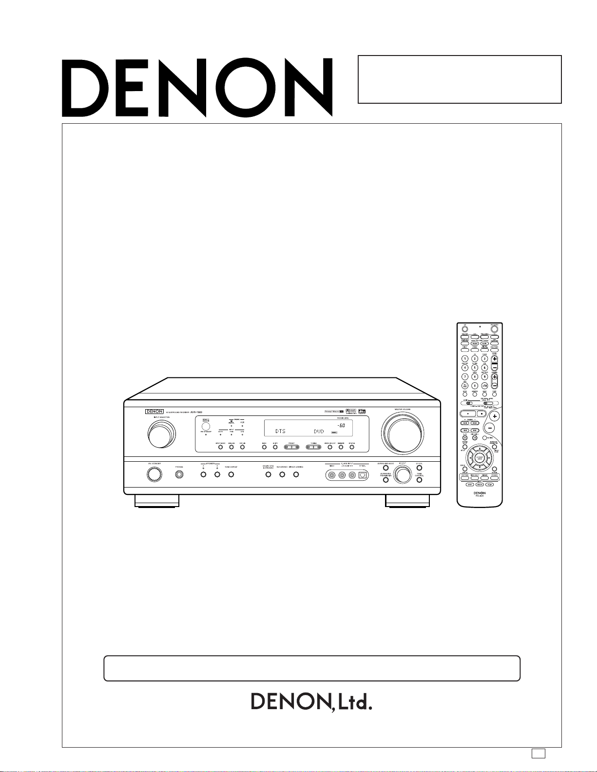
AVR-1603/683
AV SURROUND RECEIVER
Some illustrations using in this service manual are slightly different from the actual set.
16-11, YUSHIMA 3-CHOME, BUNKYOU-KU, TOKYO 113-0034 JAPAN
Telephone: 03 (3837) 5321
X0152 NC 0209
Page 2

AVR-1603/683
SAFETY PRECAUTIONS
The following check should be performed for the continued protection of the customer and service technician.
LEAKAGE CURRENT CHECK
Before returning the unit to the customer, mak e sure you make either (1) a leakage current check or (2) a line to chassis
resistance check. If the leakage current exceeds 0.5 milliamps, or if the resistance from chassis to either side of the
power cord is less than 460 kohms, the unit is defective.
SPECIFICATIONS
Audio Section
Power Amplifier
Rated output: Front: 80W+80W (8Ω/ohms, 20Hz~20kHz with 0.08% T.H.D )
Center: 80W (8Ω/ohms, 20Hz~20kHz with 0.08% T.H.D )
Surround: 80W+80W (8Ω/ohms, 20Hz~20kHz with 0.08% T.H.D )
Output terminals: Front: A or B 6 to 16Ω/ohms
LINE input - SPEAKER OUT
Input sensitivity/input impedance:
Frequency response: 10Hz~100kHz: +1, −3dB (TONE DEFEAT ON)
S/N ratio: 98dB (IHF-A weighted) (TONE DEFEAT ON)
Center/Surround: 6 to 16Ω/ohms
200mV/47kΩ/kohms
70W+70W
110W+110W (6Ω/ohms, 1kHz with 0.7% T.H.D )
100W+100W (6Ω/ohms, 1kHz with 0.7% T.H.D ) (Europe, U.K. & Australia Models)
110W+110W (6Ω/ohms, EIAJ ) (Asia Model)
70W
110W (6Ω/ohms, 1kHz with 0.7% T.H.D )
100W (6Ω/ohms, 1kHz with 0.7% T.H.D ) (Europe, U.K. & Australia Models)
110W (6Ω/ohms, EIAJ ) (Asia Model)
70W+70W
110W+110W (6Ω/ohms, 1kHz with 0.7% T.H.D )
100W+100W (6Ω/ohms, 1kHz with 0.7% T.H.D ) (Europe, U.K. & Australia Models)
110W+110W (6Ω/ohms, EIAJ ) (Asia Model)
A+B 12 to 16Ω/ohms
(8Ω/ohms, 20Hz~20kHz with 0.08% T.H.D ) (Europe, U.K., Australia & Asia)
(U.S.A., & Canada Models)
(8Ω/ohms, 20Hz~20kHz with 0.08% T.H.D ) (Europe, U.K. & Australia & Asia)
(U.S.A., & Canada Models)
(8Ω/ohms, 20Hz~20kHz with 0.08% T.H.D ) (Europe, U.K. & Australia & Asia)
(U.S.A., & Canada Models)
(U.S.A., & Canada Models)
(U.S.A., & Canada Models)
(U.S.A., & Canada Models)
Video Section
Standard video jacks
Input/output level and impedance:
Frequency response: 5Hz~10MHz +1, −3dB
1Vp-p,75Ω/ohms
S-video jacks
Input/output level and impedance:
Frequency response: 5Hz~10MHz: +1, −3dB
Y(brightness)signal 1Vp-p, 75Ω/ohms
C(color)signal 0.286Vp-p, 75Ω/ohms
Color component video jacks (U.S.A. & Canada Models)
Input/output level and impedance:
Frequency response: 5Hz~27MHz: +0, −3dB
Tuner section
Receiving range: [FM] (note: µV at 75Ω/ohms, 0dBf =1×10
U.S.A., & Canada Models:
Europe U.K. & Australia Models:
Asia Model:
Usable sensitivity: 1.0µV (11.2dBf) 18µV
50 dB quieting sensitivity: MONO 1.6µV (15.3dBf)
S/N ratio: MONO 80dB (IHF-A weighted)
T otal harmonic distortion: MONO 0.15% (1kHz)
Y(brightness)signal 1Vp-p, 75Ω/ohms
P
B/CB(blue)signal 0.7Vp-p, 75Ω/ohms
PR/CR(red)signal 0.7Vp-p, 75Ω/ohms
87.50MHz~107.90MHz 520kHz~1710kHz
87.50MHz~108.00MHz 522kHz~1611kHz
87.50MHz~107.90MHz (0.2MHz steps) 520kHz~1710kHz (10kHz steps)
87.50MHz~108.00MHz (0.05MHz steps) 522kHz~1611kHz (9kHz steps)
STEREO 23µV (38.5dBf)
STEREO 75dB (IHF-A weighted)
STEREO 0.3% (1kHz)
-15
W) [AM]
2
Page 3

General
Power supply: AC120V, 60Hz (U.S.A. & Canada Models)
AC230V, 50Hz (Europe, U.K. & Australia Models)
AC115/230V, 50/60Hz (Asia Model)
Power consumption: 4.0A (USA & Canada model)
Maximum external dimensions: 434 (W) × 147 (H) × 417 (D) mm (17-3/32″ × 5-25/32″ × 1-23/64″)
Mass: 10.4kg (22 lbs 14.9 oz)
Remote control unit (RC-920)
Batteries: R6P/AA T ype (two batteries)
External dimensions: 55 (W) × 225 (H) × 34.5 (D) mm (2-11/64″ × 8-55/64″ × 1-9/64″)
Mass: 165g (Approx. 5.8 oz) (including batteries)
* For purposes of improvement, specifications and design are subject to change without notice.
210W (Europe, U.K., Australia & Asia models)
AVR-1603/683
3
Page 4
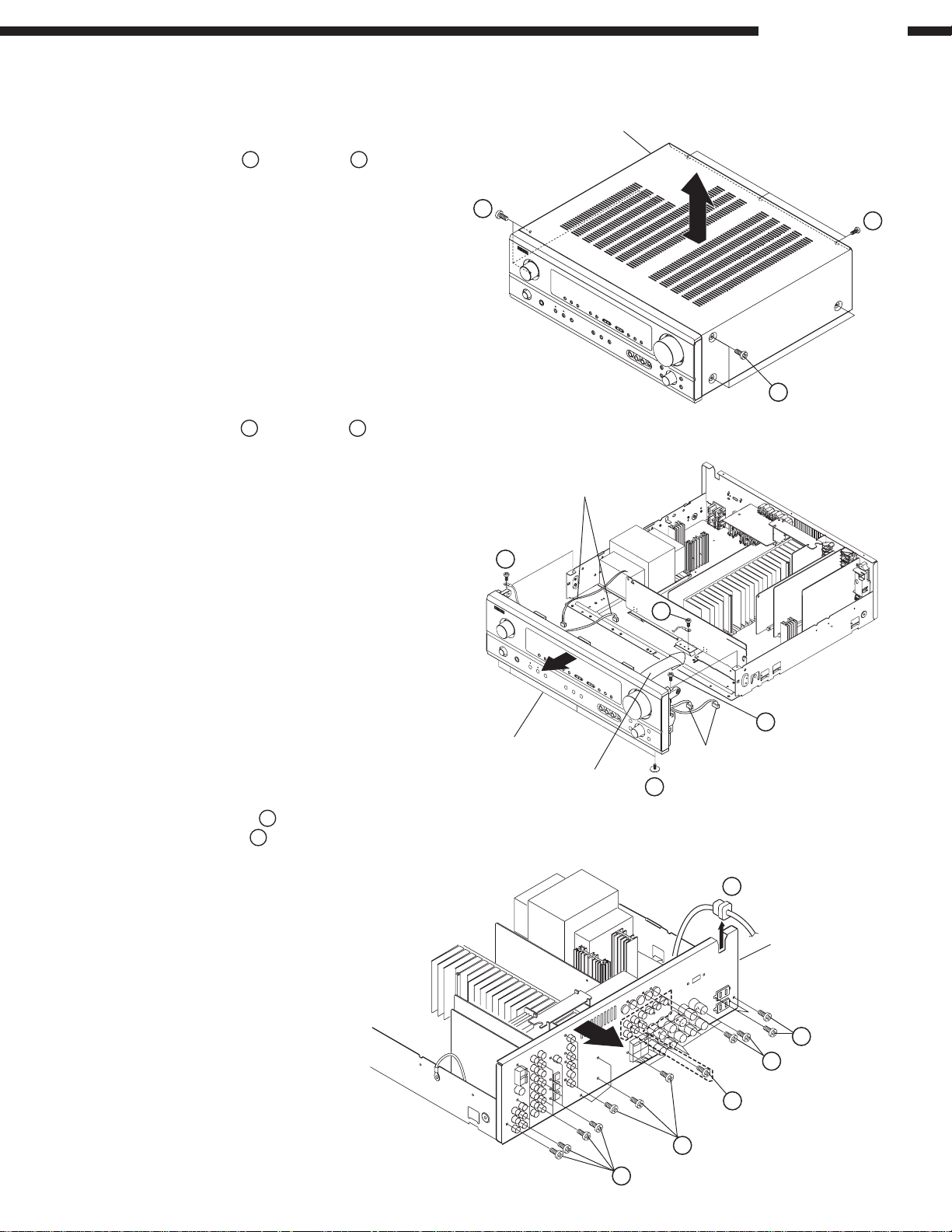
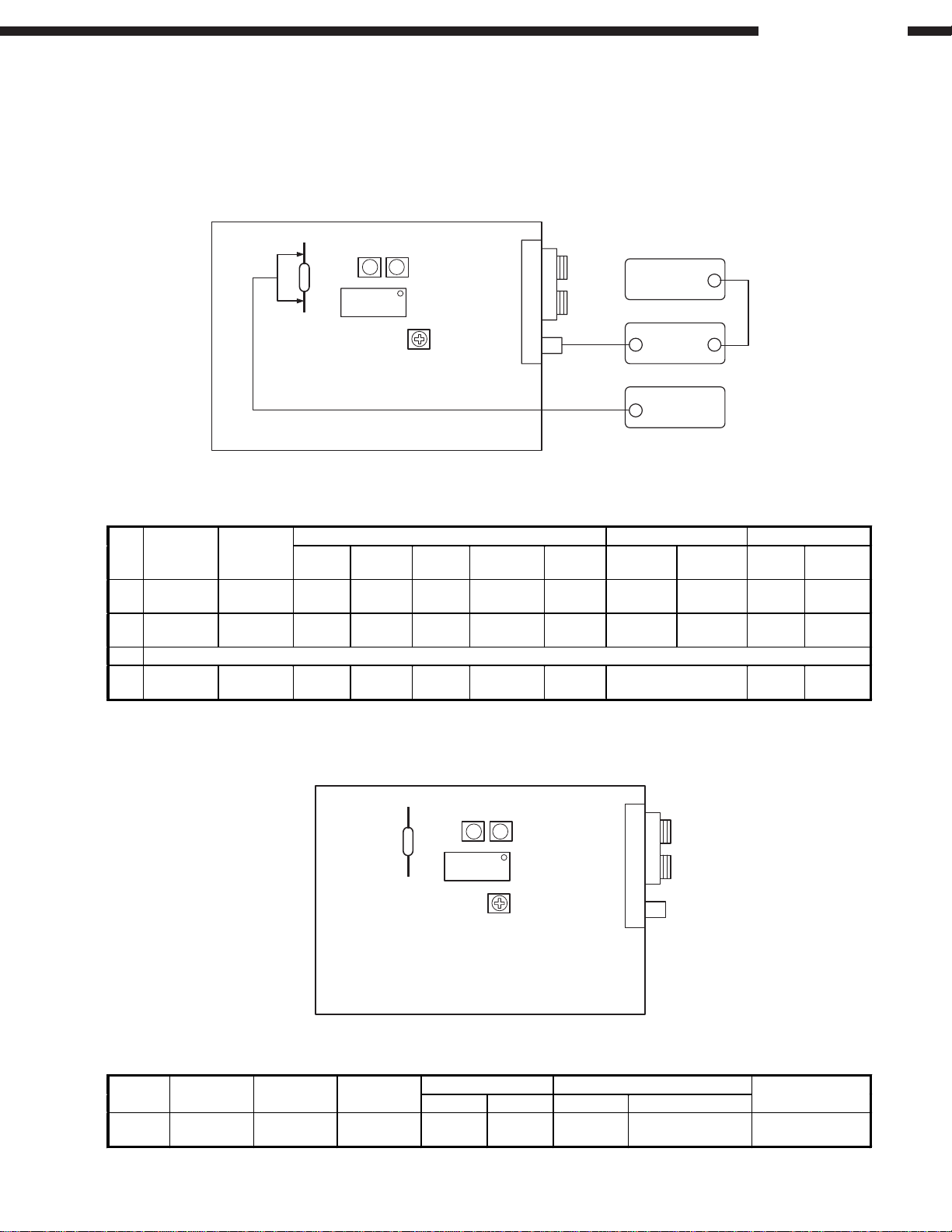
DISASSEMBLY
(Follow the procedure below in the reverse order when reassembling)
1. Top Cover
Remove 6 screws 1 and 3 screws 2, then detach the
Top Cover to the arrow direction.
AVR-1603/683
Top Cover
2. Front Panel
(1) Remove 4 screws 3 and 3 screws 4.
(2) Disconnect 3 connectors and FFC coming from the
Front Panel side.
(3) Disconnect the connector coming from the Trans., and
detach the Front Panel to the arrow direction.
1
1
Connector
4
4
2
Front Panel
3. Rear Panel
(1) Take off the AC cord 5 .
(2) Remove 32 screws 6 (36 pieces for U.S.A. & Canada models).
(3) Detach the Rear Panel to the arrow direction.
FFC
4
Connector
3
5
Rear Panel
6
6
6
(U.S.A. & Canada models)
6
6
4
Page 5
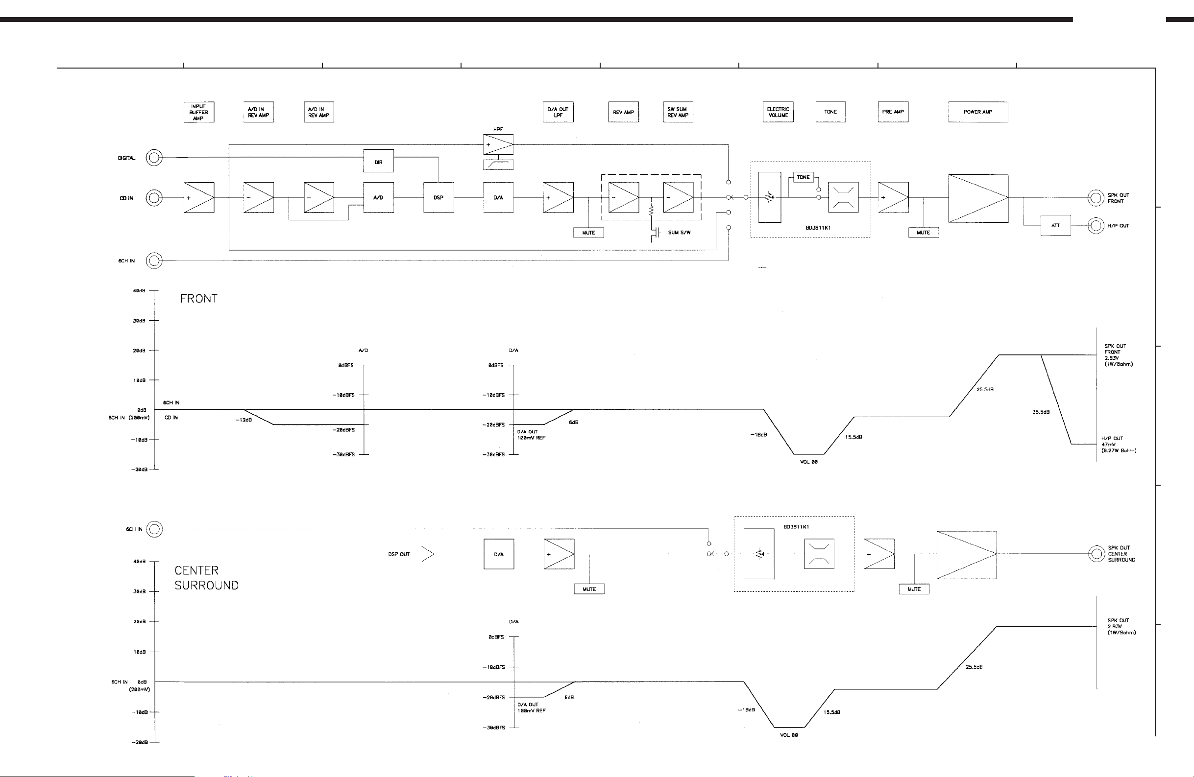
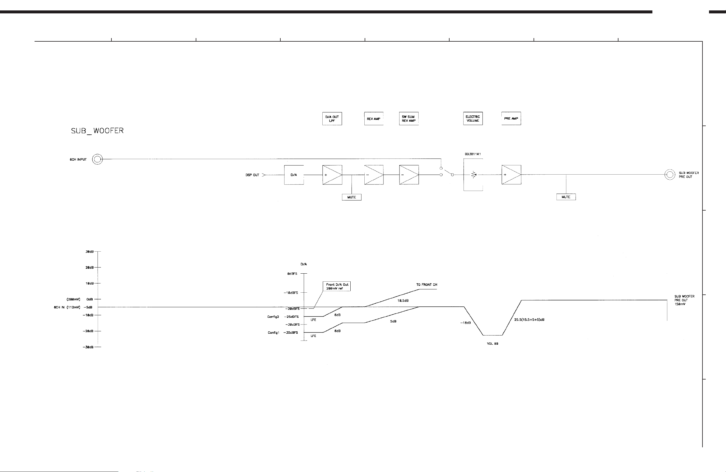
LEVEL DIAGRAMS
AVR-1603/683
1
FRONT/CENTER/SURROUND
2
3
4
5
76
8
A
B
C
D
E
5
Page 6
AVR-1603/683
1
SUB WOOFER
2
3
4
5
76
8
A
B
C
D
E
6
Page 7
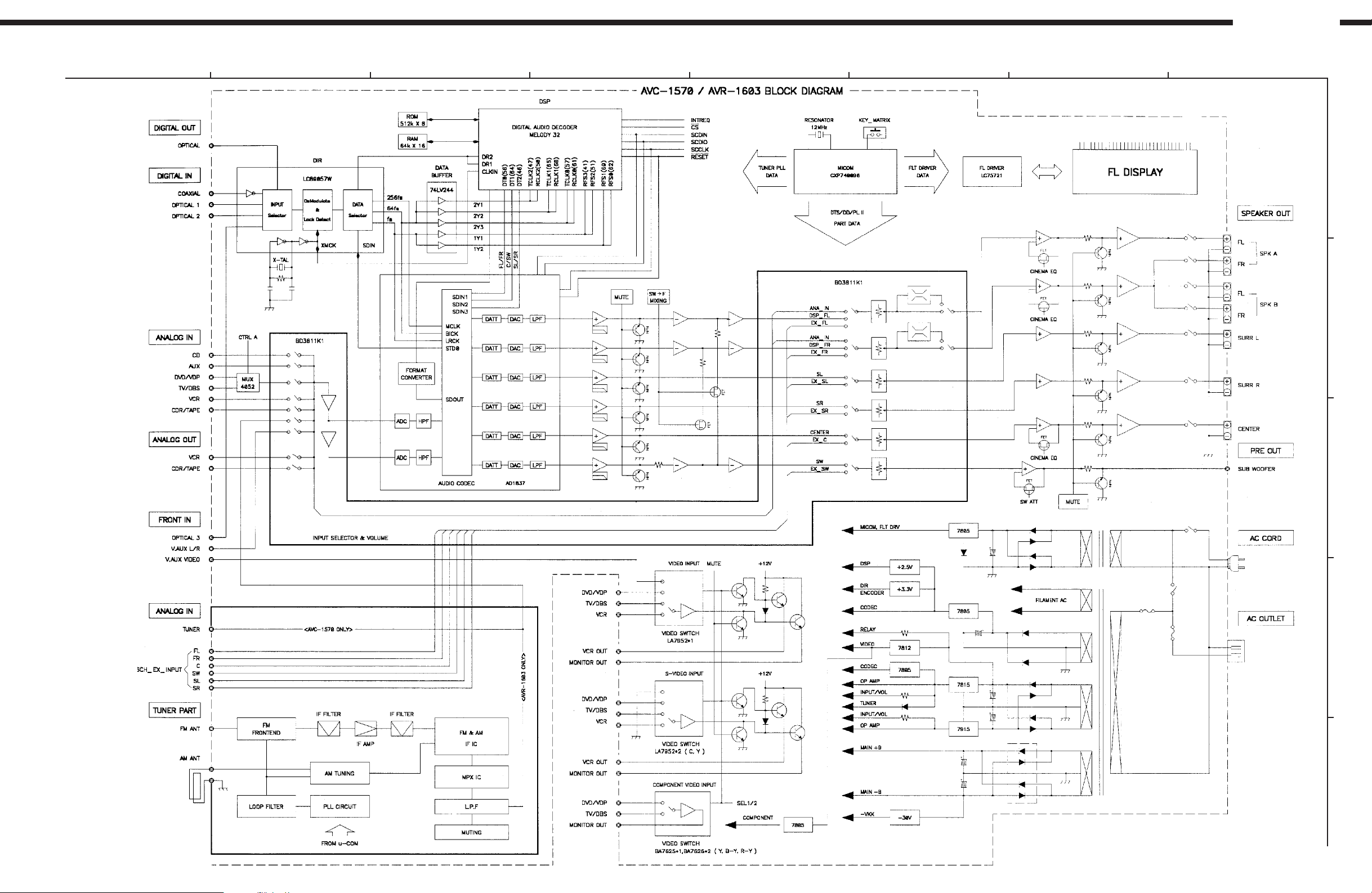
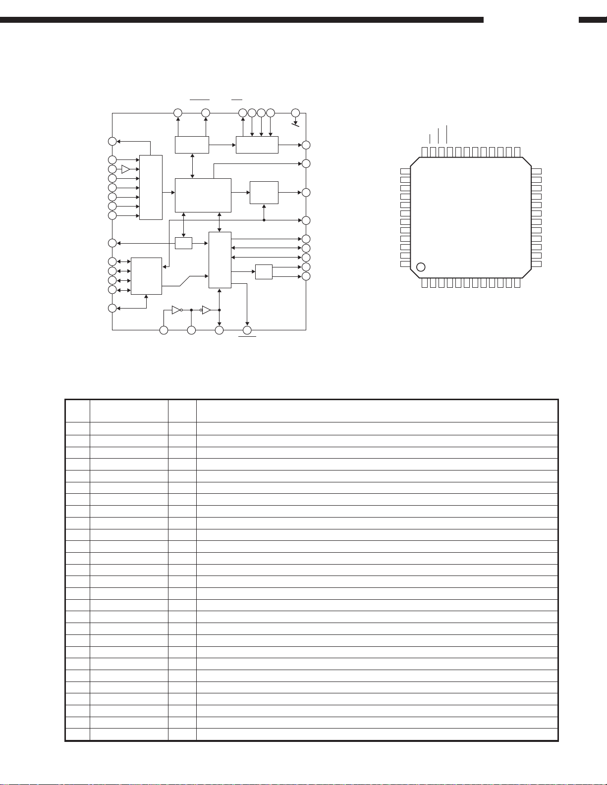
BLOCK DIAGRAM
AVR-1603/683
1
2
3
4
5
76
8
A
B
C
D
E
7
Page 8
ADJUSTMENT
Tuner Section
CONNECTION DIAGRAM OF MEASURING INSTRUMENTS
FM
T402T403
R471
IC402
AVR-1603/683
STEREO
MODULATOR
VR402
TUNER B'D
FM ALIGNMENT
Alignment
Step
AM
Item
Center
1
Adjustment
2 Distortion
3 Repeat Steps 1 and 2
4 Signal Level
Tuning
Frequency
Setting
98.1MHz
(98.0MHz)
98.1MHz
(98.0MHz)
98.1MHz
(98.0MHz)
Type Frequency
FM SSG 98.1MHz 60dBµ
FM SSG 98.1MHz 60dBµ
FM SSG 98.1MHz 20dBµ OFF
Input Output Adjustment
Input
Level
Modulation Coupling Type Connect to Points Adjust to
Mono
1kHz 100%
Mono
1kHz 100%
75ohm
Antenna
Terminal
Antenna
Terminal
Antenna
Terminal
FM SSG
Digital
Voltmeter
Digital
Voltmeter
Distortion
Meter
Light “TUNED” on
Terminal (L)
FL Display
R471 T402 ± 50mV
Output
T403
VR402
Minimum
Distortion
+14
20
−10
dB
AM ALIGNMENT
Step
1 Signal Level
Alignment
Item
Frequency Input
999 (1000)
kHz
AM SSG
T402T403
R471
IC402
VR401
TUNER B’D
Output Adjustment
Type Connect to Points Adjust to
VR401
Light “TUNED” on
FL Display
Remarks
SSG OUTPUT
74dBµ (EMF)
8
Page 9
AVR-1603/683
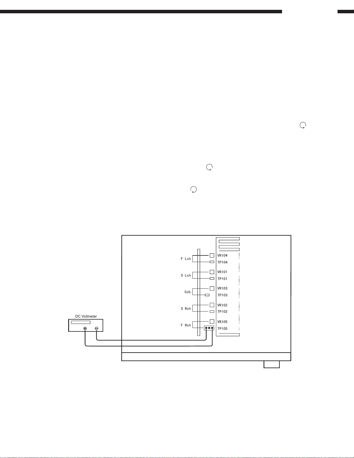
Audio Section
Idling Current
Required measurement equipment : DC Voltmeter
Preparation
(1) Avoid direct blow from an air conditioner or an electric fan, and adjust the unit at normal room tempereture
15 °C ~ 30 °C (59 °F ~ 86 °F).
(2) Presetting
● POWER (Power sourse switch) → OFF
● SPEAKER (Speaker terminal) → No load (Do not connect speaker, dummy resistor, etc.)
Adjustment
(1) Remove top cover and set VR101, VR102, VR103, VR104, VR105 on Amp. Unit at full counterclockwise ( )
position.
(2) Connect DC Voltmeter to test points (FRONT-Lch: TP104, FRONT-Rch: TP105, CENTER ch: TP103,
SURROUND-Lch: TP101, SURROUND-Rch: TP102).
(3) Connect power cord to AC Line, and turn power switch "ON".
(4) Presetting. MASTER VOLUME : "---" counterclockwise (
MODE : 5CH STEREO
FUNCTION : CD
(5) Within 2 minutes after the power on, turn VR101 clockwise (
DC.
(6) After 10 minutes from the preset above, turn VR101 to set the voltage to 2.5 mV ±0.5 mV DC.
(7) Adjust the Variable Resistors of other channels in the same way.
min.)
) to adjust the TEST POINT voltage to 1.5 mV ±0.5 mV
9
Page 10
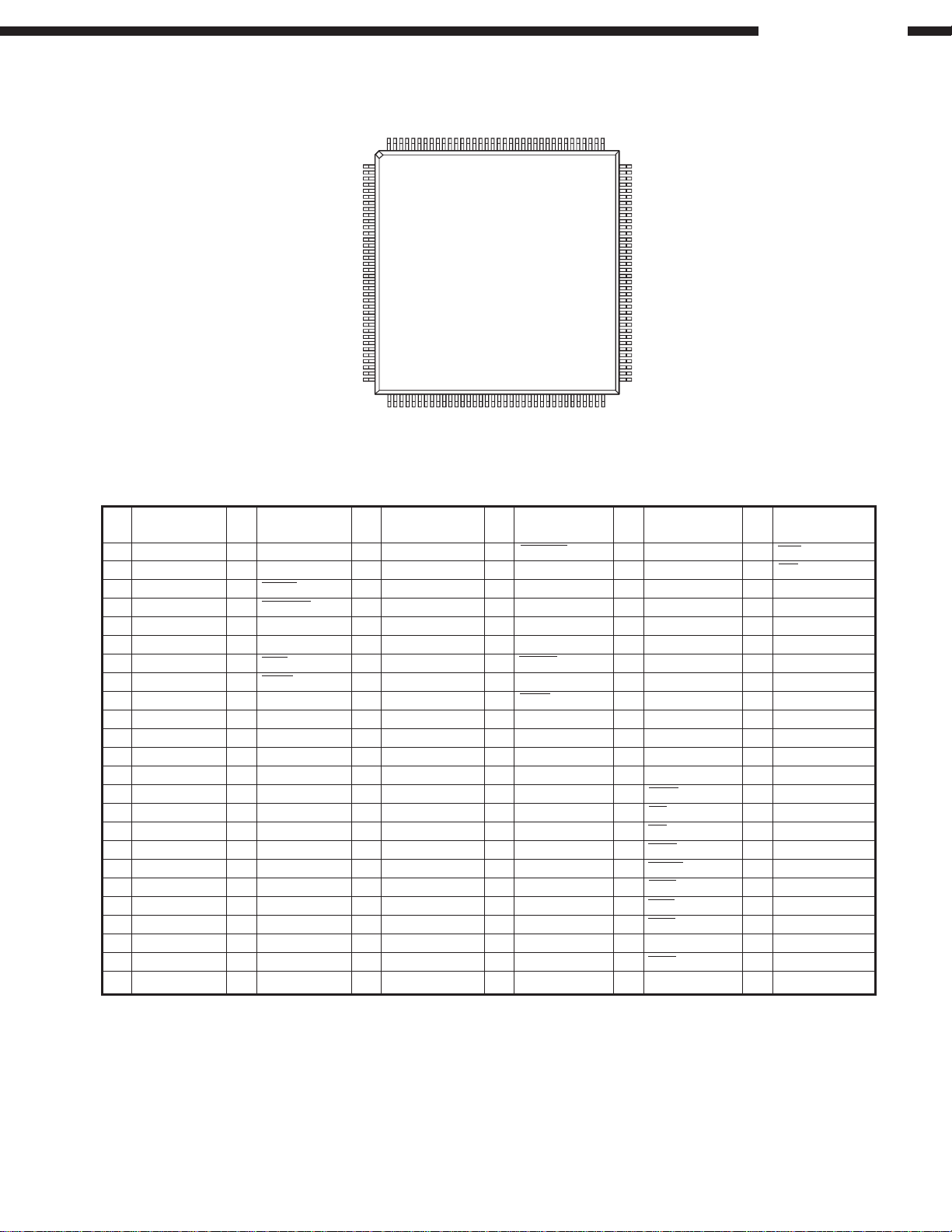
SEMICONDUCTORS
PH7
PH6
PH5
PH4
PH3
PH2
PH1
PH0
PK7/TO1
RST
V
SS
XTAL
EXTAL
PK6/CS0
PK5/SI0
PK4/SO0
PK3/SCK0
PF7/AN11
PF6/AN10
PF5/AN9
PC6
PC7
PA0
PA1
PA2
PA3
PA4
PA5
PA6
PA7NCV
DDVSS
PK1/TX
PK2/TEX
PI1/RMC
PI2/NMI
PI3/TO0/ADJ
PI4/INT1/CS1
PI5/SCK1
PC5
PC4
PC3
PC2
PC1
PC0
PB7/SI2
PB6/SO2
PB5/SCK2
PB4/TO2
PB3
PB2
PB1
PB0
PJ7
PJ6
PJ5
PJ4
PJ3
PJ2
PJ1
PJ0
PD7
PD6
PD5
PD4
PD3
PD2
PD1
PD0
PI6/SO1
PI7/SI1
PE0/INT0
PE1/INT2
PE2/PWM0
PE3/PWM1
PE4
PE5
PE6
PE7
PG0/TxD
PG1/RxD
PG2/EC0
PG3/EC1
PG4/EC2
PG5/INT3
PG6/INT4
PG7/CINT
AN0
AN1
AN2
AN3
PF0/AN4
PF1/AN5
PF2/AN6
PF3/AN7
AV
DD
AV
REF
AV
SS
PF4/AN8
1
2
3
4
5
6
7
8
9
10
11
12
13
14
15
16
17
18
19
20
31323334353637383940414243444546474849
50
100
99989796959493929190898887868584838281
21
22
23
24
25
26
27
28
29
30
80
79
78
77
76
75
74
73
72
71
70
69
68
67
66
65
64
63
62
61
60
59
58
57
56
55
54
53
52
51
TOP VIEW
IC’s
CXP740096
(IC201)
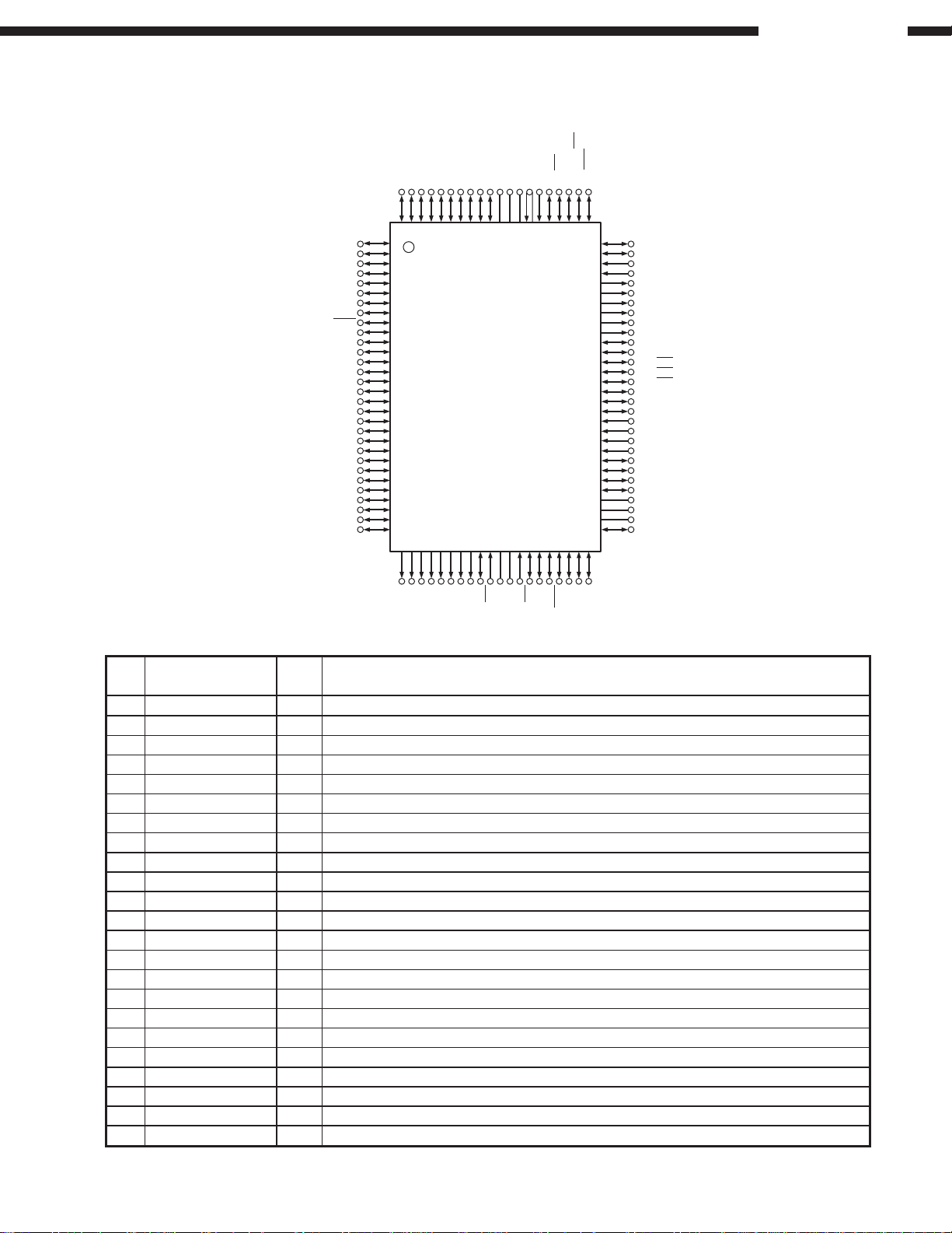
AVR-1603/683
CXP740096 Terminal Function
Pin
No.
1 3811K1MUTE O BD3811K1 CONTROL
2 3811K1CLK O BD3811K1 CONTROL
3 3811K1DATA O BD3811K1 CONTROL
4 CDR/TAPE O CDR/TAPE INHIBIT
5 VCR O VCR INHIBIT
6 ERR MUTE O ERR MUTE
7 ERR MUTE OFF O ERR MUTE OFF
8 89057 AUDIO I LC89057 CONTROL
9 89057 EMPHA I LC89057 CONTROL
10 SW SUM O SW SUMMING CONTROL
11 M32 SDIN I DATA INPUT FROM MELODY32
12 89057 SDIN I DATA INPUT FROM LC89057
13 EPROM RESET O EPROM RESET
14 89057 RESET O LC89057 RESET
15 M32 CS O MELODY32 CS
16 M32 SDOUT O MELODY32 CONTROL DATA
17 89057 CE O LC89057 CE
18 89057 SDOUT O CONTROL DATA
19 89057 SCLK O CONTROL CLOCK
20 1837 RESET O CODEC RESET
21 NC
22 SW MUTE O SW MUTE
23 RELAY F-B O FRONT B RELAY
Pin Name FunctionI/O
10
Page 11
AVR-1603/683
Pin
No.
Pin Name FunctionI/O
24 RELAY F-A O FRONT A RELAY
25 RELAY SURR O SURROUND RELAY
26 RELAY CNT O CENTER RELAY
27 RELAY H/P O H/P RELAY
28 FUNC UP I ENCODER INPUT(FUNCTION)
29 H/P DETECT I H/P DETECT
30 FUNC DOWN I ENCODER INPUT(FUNCTION)
31 NC
32 CNT MUTE O CENTER MUTE
33 FRONT MUTE O FRONT MUTE
34 SURR MUTE O SURROUND MUTE
35 NC
36 NC
37 NC
38 FL DRV RESET O LC75721NE RESET
39 RELAY POWER O POWER RELAY
40 RESET I RESET
41 GND I
42 XTAL
43 EXTAL
44 FL DRV CE O LC75721NE CE
45 FL DRV DATA O LC75721NE DATA
46 FL DRV/2090 CLK O CONTROL CLOCK
47 2090 DATA O BU2090F DATA
48 VOL DOWN I ENCODER INPUT(VOLUME)
49 VOL UP I ENCODER INPUT(VOLUME)
50 SEL DOWN I ENCODER INPUT(SELECT)
51 SEL UP I ENCODER INPUT(SELECT)
52 AVSS
53 VREF
54 AVDD
55 NC
56 GND
57 STEP OPT I AREA SELECT
58 SET OPT I MODEL SELECT
59 GND
60 KEY IN3 I KEY INPUT
61 KEY IN2 I KEY INPUT
62 KEY IN1 I KEY INPUT
63 9K/10K STEP I TUNER STEP SELECT
64 PROTECT I PROTECTION
65 89057 INT I LC89057 INTERUPT
66 M32 SCLK O MELODY32 CLOCK
67 1837 CE O CODEC CE
68 M32 RESET O MELODY32 RESET
69 NC
70 NC
71 NC
72 NC
73 NC
74 NC
75 NC
76 NC
11
Page 12
AVR-1603/683
Pin
No.
Pin Name FunctionI/O
77 PWR DOWN I POWER DOWN DETECT
78 RDS CLK O TDA7330 CONTROL CLOCK
79 RDS DATA O TDA7330 CONTROL DATA
80 NC
81 VIDEO MUTE O VIDEO MUTE
82 M32 INTREQ I/O MELODY32 CONTROL
83 VIDEO SEL1 O VIDEO SELECT1
84 VIDEO SEL2 O VIDEO SELECT2
85 REMOCON I REMOTE CONTROL SIGNAL INPUT
86 GND
87 GND
88 VSS
89 VDD
90 NC
91 NC
92 PLL DATA O PLL CONTROL
93 PLL CLK O PLL CONTROL
94 PLL DT IN O PLL CONTROL
95 TU MUTE O TUNER MUTE
96 STEREO I STEREO DETECT
97 TUNED I TUNED DETECT
98 PLL CE O PLL CONTROL
99 NC
100 NC
12
Page 13
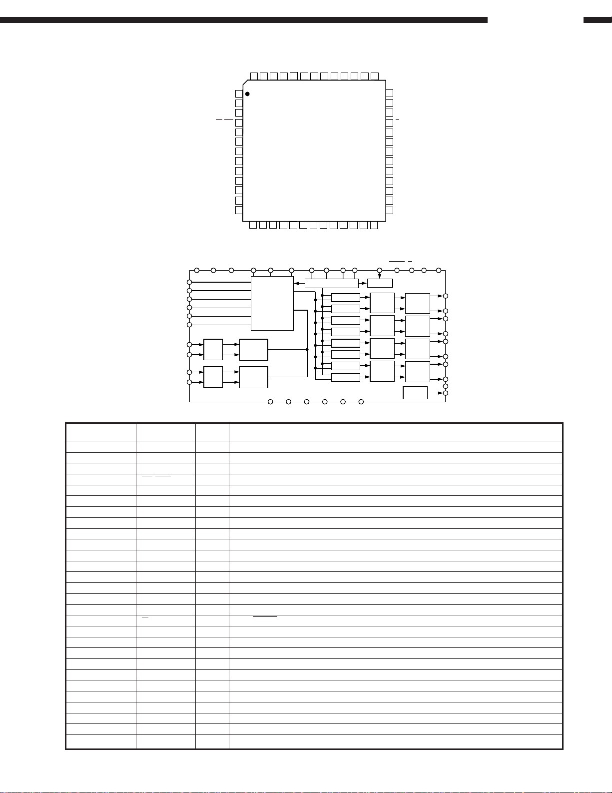
MELODY32 (IC802)
AVR-1603/683
MELODY32 Terminal Function
Pin
Pin Name
No.
1 D14
2 D15
3 HAD0
4 HAD1
5 GND
6 HAD2
7 HAD3
8 HAD4
9 HAD5
10 HAD6
11 HAD7
12 HAD8
13 VDDEXT
14 HAD9
15 HAD10
16 GND
17 HAD11
18 HAD12
19 VDDINT
20 HAD13
21 HAD14
22 HAD15
23 HA16
24 HACK_P
Pin
Pin Name
No.
25 VDDEXT
26 HACK
27 HCMS
28 HCIOMS
29 GND
30 HALE
31 HRD
32 HWR
33 GND
34 PF0
35 PF1
36 PF2
37 PF3
38 PF4
39 PF5
40 VDDEXT
41 PF6
42 PF7
43 TMR0
44 TMR1
45 TMR2
46 DT2
47 TCLK2
48 TFS2
144
1
36
37
Pin
Pin Name
No.
49 DR2
50 RCLK2
51 RFS2
52 RXD
53 TXD
54 GND
55 GND
56 DT0
57 TCLK0
58 VDDINT
59 TF50
60 DR0
61 RCLK0
62 RFS0
63 VDDEXT
64 DT1
65 TCLK1
66 TFS1
67 DR1
68 RCLK1
69 RFS1
70 BMODE0
71 BMODE1
72 BYPASS
TOP VIEW
Pin
No.
73 RESET
74 TDO
75 TDI
76 TMS
77 GND
78 TCK
79 TRST
80 GND
81 EMU
82 VDDINT
83 OPMODE
84 A0
85 A1
86 A2
87 A3
88 A4
89 A5
90 VDDEXT
91 A6
92 A7
93 A8
94 GND
95 A9
96 A10
Pin Name
109
108
73
72
Pin
No.
97 A11
98 A12
99 A13
100 VDDEXT
101 A14
102 A15
103 A16
104 A17
105 GND
106 A18
107 A19
108 A20
109 A21
110 BGH
111 BG
112 BR
113 BMS
114 IOMS
115 MS0
116 MS1
117 MS2
118 VDDEXT
119 MS3
120 ACK
Pin Name
Pin
No.
Pin Name
121 WR
122 RD
123 D0
124 D1
125 D2
126 D3
127 VDDINT
128 D4
129 GND
130 CLKOUT
131 VDDEXT
132 CLKIN
133 XTAL
134 GND
135 D5
136 D6
137 D7
138 D8
139 D9
140 D10
141 D11
142 D12
143 VDDEXT
144 D13
13
Page 14
AD1837 (IC808)
DVDD
CLATCH
CIN
PD/RST
AGND
NC
OUTL1
NC
OUTR1
AGND
AVDD
NC
OUTL2
DGND
CCLK
COUT
ASDATA
ODVDD
MCLK
ALRCLK
ABCLK
ADCLP
ADCLN
DSDATA4
ADCRN
50 494847 46 45 44 43 42 41 40
51
52
1
2
3
4
5
6
7
8
9
10
11
12
13
14 15 16 17 18 19 20 21 22 23 24 25 26
NC
OUTR2
TOP VIEW
FILTD
FILTR
AGND
AVDD
DSDATA3
DSDATA2
AGND
ADCRP
DGND
DSDATA1
NC
OUTL3
39
38
37
36
35
34
33
32
31
30
29
28
27
AVR-1603/683
DVDD
DBCLK
DLRCLK
M/S
AGND
OUTR4
NC
OUTL4
NC
AGND
AVDD
OUTR3
NC
MCLKASDATAABCLKALRCLKODVDDDVDD DVDD
PD/RST M/S AVDD AVDD
CLOCK
DIGITAL
FILTER
DIGITAL
FILTER
DIGITAL
FILTER
DIGITAL
FILTER
DescriptionPin No.
V
Σ-∆
DAC
Σ-∆
DAC
Σ-∆
DAC
Σ-∆
DAC
REF
OUTL1
OUTR1
OUTL2
OUTR2
OUTL3
OUTR3
OUTL4
OUTR4
FILTD
FILTR
DLRCLK
DBCLK
DSDATA1
DSDATA2
DSDATA3
DSDATA4
ADCLP
ADCLN
ADCRP
ADCRN
AD1837 Terminal Function
Pin Name
Σ-∆
ADC
Σ-∆
ADC
AD1837
Input/
Output
SERIAL DATA
I/O PORT
DIGITAL
FILTER
DIGITAL
FILTER
CINCLATCHCCLK COUT
CONTROL PORT
VOLUME
VOLUME
VOLUME
VOLUME
VOLUME
VOLUME
VOLUME
VOLUME
DGND AGND AGND AGND AGNDDGND
1,39 DVDD Digital Power Supply. Connect to digital 5V supply.
2 CLATCH I Latch Input for Control Data
33 CIN I Serial Control Input
4 PD/RST I Power-Down/Reset
5,10,16,24,30,35 AGND Analog Ground
6,12,25,31 NC Not connected
7,13,26,32 OUTLx O DACx Left Channel Output
8,14,27,33 NC Not connected
9,15,28,34 OUTRx O DACx Right Channel Output
11,19,29 AVDD Analog Power Supply. Connect to analog 5V supply.
17 FILTD Filter Capacitor Connection. Recommend 10µF/100nF.
18 FILTR Reference Filter Capacitor Connection. Recommended 10µF/100nF.
20 ADCLN I ADC Left Channel Negative Input
21 ADCLP I ADC Left Channel Positive Input
22 ADCRN I ADC Right Channel Negative Input
23 ADCRP I ADC Right Channel Positive Input
36 M/S I ADC Master/Slave Select
37 DLRCLK I/O DAC LR Clock
38 DBCLK I/O DAC Bit Clock
40,52 DGND Digital Ground
41-44 DSDATAx I DACx Input Data (Left and Right Supply)
45 ABCLK I/O ADC Bit Clock
46 ALRCLK I/O ADC LR Clock
47 MCLK I Master Clock Input
48 ADVDD Digital Output Driver Power Supply
49 ASDATA O ADC Serial Data Output
50 COUT O Output for Control Data
51 CCLK I Control Clock Input for Control Data
14
Page 15
LC89057W (IC807)
AVR-1603/683
RXOUT
RX0
RX1
RX2
RX3
RX4
RX5/VI
RX6/UI
LPF
TMCK/PIO0
TBCK/PIO1
TLRCK/PIO2
TDATA/PIO3
TXO/PIOEN
1
2
3
4
5
8
9
10
13
44
45
46
47
48
EMPHA/UO33AUDIO/VO35INT40CL39CE38DI
32
Clock
Selector
27
Microcontroller
Input
Selector
Modulation
or
Parallel Port
XIN
29
C bit, U bit
Demodulation
&
Lock Detect
PLL
28
XOUT
XMCK34CKST
I/F
Data
Selector
I/N
XMODE
41
37
36
21
24
16
17
20
22
23
DO
RERR
RDATA
SDIN
RMCK
RBCK
RLRCK
SBCK
SLRCK
36 RERR1RXOUT
35 INT2RX0
34 CKST3RX1
TOP VIEW
33 AUDIO/VO4RX2
32 EMPHA/UO5RX3
31 DGND6DGND
30 DVDD7DVDD
29 XIN8RX4
28 XOUT9RX5/VI
27 XMCK10RX6/UI
26 DVDD11DVDD
25 DGND12DGND
24 SDIN37DO
23 SLRCK38DI
22 SBCK39CE
21 RDATA40CL
20 RLRCK41XMODE
19 DVDD42DGND
18 DGND43DVDD
17 RBCK44TMCK/PIO0
16 RMCK45TBCK/PIO1
15 AGND46TLRCK/PIO2
14 AVDD47TDATA/PIO3
13 LPF48TXO/PIOEN
LC89057W Terminal Function
Pin
No.
1 RXOUT O Input bi-phase select data output terminal
2 RX0 I5 TTL compatible digital data input terminal
3 RX1 I Coaxial compatible amp built-in digital data input terminal
4 RX2 I5 TTL compatible digital data input terminal
5 RX3 I5 TTL compatible digital data input terminal
6 DGND — Digital GND
7 DVDD — Digital power
8 RX4 I5 TTL compatible digital data input terminal
9 RX5/VI I5 TTL compatible digital data/Validity flag input terminal for modulation
10 RX6/UI I5 TTL compatible digital data/User data input terminal for modulation
11 DVDD — Digital power for PLL
12 DGND — Digital GND for PLL
13 LPF O PLL loop filter connecting terminal
14 AVDD — Analog power for PLL
15 AGND — Analog GND for PLL
16 RMCK O RMCK clock output terminal (256fs, 512fs, XIN, VCO)
17 RBCK O/I RBCK clock in/output terminal (64fs)
18 DGND — Digital GND
19 DVDD — Digital power
20 RLRCK O/I RLRCK clock in/output terminal (fs)
21 RDATA O Serial audio data output terminal
22 SBCK O SBCK clock output terminal (32fs, 64fs, 128fs)
23 SLRCK O SLRCK clock output terminal (fs/2, fs, 2fs)
24 SDIN I5 Serial audio data input terminal
25 DGND — Digital GND
26 DVDD — Digital power
27 XMCK O Osc. amp output terminal
Pin Name
I/O
Function
15
Page 16
AVR-1603/683
Pin
No.
Pin Name I/O
Function
28 XOUT O X’tal osc. connecting output terminal
29 XIN I X’tal osc. connection, external clock input terminal (24.576MHz or 12.288MHz)
30 DVDD — Digital power
31 DGND — Digital GND
32 EMPHA/UO I/O Emphasis information/U-data output/Chip address setting terminal
33 AUDIO/VO I/O Non-PCM detect/V-flag output/ Chip address setting terminal
34 CKST I/O Clock switch transition period output/Demodulation master or slave function switching terminal
35 INT I/O Interrupt output for µcom (Interrupt factor selectable)/Modulation or general I/O switching terminal
36 RERR O PLL lock error, data error flag output
37 DO O µcom I/F, read out data output terminal (3-state)
38 DI I5 µcom I/F, write data input terminal
39 CE I5 µcom I/F, chip enable input terminal
40 CL I5 µcom I/F, clock input terminal
41 XMODE I5 System reset input terminal
42 DGND — Digital GND
43 DVDD — Digital power
44 TMCK/PIO0 I/O 256fs system clock input for modulation/General I/O in/output terminal
45 TBCK/PIO1 I/O 64fs bit clock input for modulation/General I/O in/output terminal
46 TLRCK/PIO2 I/O fs clock input for modulation/General I/O in/output terminal
47 TDATA/PIO3 I/O Serial audio data input for modulation/General I/O in/output terminal
48 TXO/PIOEN O/I Modulation data output/ General I/O enable input terminal
* For latch-up countermeasure, perform each power supply ON/OFF in the same timing.
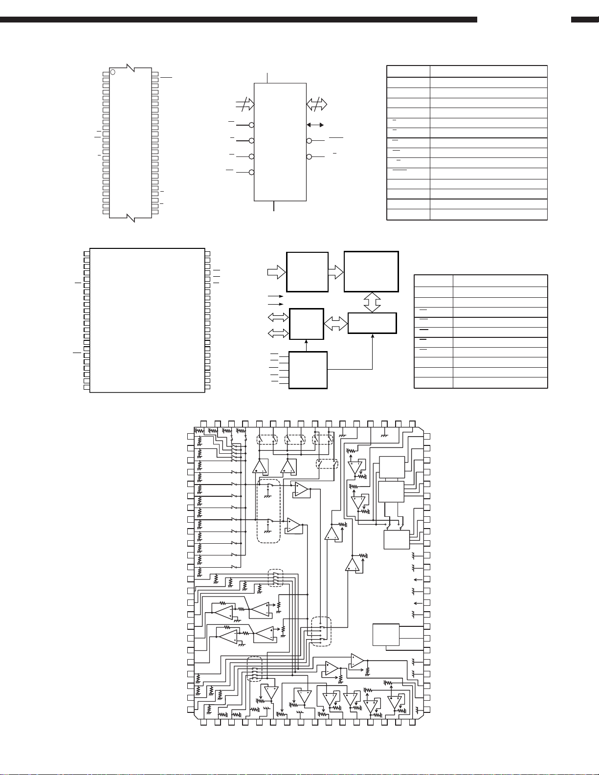
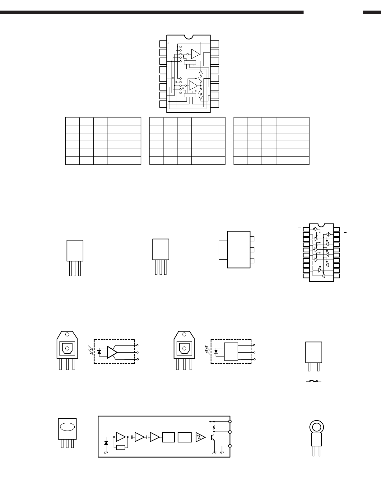
LC72131 (IC401)
1
XIN
CE
2
3
DI
4
CL
DO
5
BO1
6
BO2
7
BO3
8
BO4
9
IO1
10
LA1266 (IC402)
AM-IF FM-IF FM-IN
11
13
18
AM-IN
20
RF MIX
21
REG
22
BUFFER
124
XOUT
20
Vss
19
AOUT
18
17
AIN
PD
16
VDD
15
FMIN
14
12 13
10
IF
IF
BUFFER
OSC
23
2
1
FM - IF
AM-IF DET
OSC
NARROW
BUFFER
S-METER
GND
24
4
3
5
6
7
Vcc
POST
Q.D.
AMP
AGC
S-METER
17
19
14
16
LED
DRIVER
12
9
15
8
LA3401 (IC403)
22
VOL
REG
SYMMETRICAL
REOCTANCE
CIRCUIT
MUTING
21
OSC
FF
AMIN
13
IO2
12
IFIN
11
FM AM CHANGE
20
PHASE
COMPARATOR
FF
Ro
19
FF
38kHz
DECODER
18
VCO STOP
38kHz 90°
Rc
Rc
16
17
PILOT DET
FF
FF
19kHz 90°
MUTING CONTROL
FM AM CHANGE OVER
Rb
Rb
15
Vcc ON
MUTING
14
13
LAMP
DRIVER
TRIGGER
STEREO
SWITCH
MUTING
OUTPUT
12
2
1
4
3
6
5
8
7
9
11
10
16
Page 17
AVR-1603/683
M29W800AT (IC805)
M29W800T
M29W800T
48
37
36
25
1
A15 A16
A14 BYTE
A13 V
A12 DQ15A-1
A11 DQ7
A10 DQ14
A9 DQ6
A8 DQ13
NC DQ5
NC DQ12
W DQ4
12
RP V
13
NC DQ11
NC DQ3
RB DQ10
A18 DQ2
A17 DQ9
A7 DQ1
A6 DQ8
A5 DQ0
A4 G
A3 V
A2 E
A1 A0
24
IS61LV6416 (IC806)
1
A15
2
A14
3
A13
4
A12
5
A11
6
CE
7
I/O0
8
I/O1
9
I/O2
10
I/O3
11
Vcc
12
GND
13
I/O4
14
I/O5
15
I/O6
16
I/O7
17
WE
18
A10
19
A9
20
A8
21
A7
22
NC
V
SS
CC
A0-A18
19
15
DQ0-DQ14
W
E
M29W800AT
G
DQ15A-1
BYTE
RB
RP
SS
V
ss
A0
44
A1
43
A2
42
OE
41
UB
40
LB
39
I/O15
38
I/O14
37
I/O13
36
I/O12
35
GND
34
Vcc
33
I/O11
32
I/O10
31
I/O9
30
I/O8
29
NC
28
A3
27
A4
26
A5
25
A6
24
NC
23
A0-A15
VCC
GND
I/O0-I/O7
Lower Byte
I/O8-I/O15
Upper Byte
CE
OE
WE
UB
LB
DECODER
I/O
DATA
CIRCUIT
CONTROL
CIRCUIT
64K x 16
MEMORY ARRAY
COLUMN I/O
Symbol
A0-A18
DQ0-DQ7
DQ8-DQ14
DQ15A-1
E
G
W
RP
CC
SS
PIN DESCRIPTION
Symbol
A0-A15
I/O0-I/O15
CE
OE
WE
LB
UB
V
CC
Address Inputs
Data Input/Outputs, Command Inputs
Data Input/Outputs
Data Input/Output or Address Input
Chip Enable
Output Enable
Write Enable
Reset/Block Temporary Unprotect
Ready/Busy OutputRB
Byte/Word OrganizationBYTE
Supply VoltageV
GroundV
No Connected InternallyNC
Don’t Use as Internally ConnectedDU
Pin Name
Pin Name
Address inputs
Data Inputs/Outputs
Chip Enable Input
Output Enable Input
Write Enable Input
Lower-byte Control (I/O0-I/O7)
Upper-byte Control (I/O8-I/O15)
No ConnectionNC
Power
GroundGND
CC
PIN DESCRIPTION
BD3811K1 (IC701)
IN61
INDVDSR
INDVDSL
INDVDC
INDVDSW
OUT2(+)
OUT2(-)
OUT1(+)
OUT1(-)
IN1DSP
IN1MIX
IN2DSP
IN2MIX
IN22
IN21
IN12
IN11
ROUT32
ROUT31
ROUT22
ROUT21
ROUT12
ROUT11
5.1ch Mode SW1
VINC
GOUTC
AGND10
OUTSW
80 79 78 77 76 75 74 73 72 71 70 69 68 67 66 65
IN31
1
IN32
2
IN41
3
IN42
4
IN51
5
IN52
6
7
IN62
8
IN71
9
IN72
10
IN81
IN82
11
12
13
14
15
16
17
18
19
20
21
22
23
24
25 26
INDSPSR
5.1ch Mode SW2 DSP
INDSPSL
5.1ch Mode SW2 DVD
27 28 29 30 31 32 33 34 35 36 37 38 39 40
VINSW
INDSPC
INDSPSW
AGND1
GOUTSW
AGND2
GOUT2
OUTC
VIN2
OUTSL
TREBLE
LOGIC
AGND9
BASS
BASS
BOOST
OUTSR
GOUT1
VINSL
VIN1
GOUTSL
64
63
62
61
60
59
58
57
56
55
54
53
52
51
50
49
48
47
46
45
44
43
42
41
TNF2
TNF1
BNF11
BNF21
BNF12
BNF22
BBNF2
OUT2
BBNF1
OUT1
AGND8
AGND7
VCC
AGND6
VEE
AGND5
MUTE
CL
DA
DGND
AGND4
GOUTSR
VINSR
AGND3
17
Page 18
AVR-1603/683
LC75721E (IC301)
G7 G8G9
G10
G11
AA8/G12
AA7/G13
AA6/G14
48 33
49
DI
CL
CE
RES
DD
V
OSCI
OSCO
Vss
TEST
FL
V
G1
G2
G3
G4
G5
G6
64
AM 1
AM 2
AM 3
AM 4
AM 5
AM 6
AM 7
AM 8
74LCX74 (IC821)
1C
D1
CP
1
D
D
1
2
CP
1
3
S
D1
4
Q
1
5
Q
1
6
GND Q
7
SD1C
Q1Q
D
2
CD2S
Q2Q
1
D1
1
CP
2
D2
2
MM74LCX244 (IC809~811)
LC75721E Terminal Function
AA5/G15
AA4/G16
AA3
AA2
AA1
AM35
AM34
AM33
32
AM 17
AM 18
AM 19
AM 20
AM 21
AM 22
AM 23
AM 24
AM 25
AM 26
AM 27
AM 28
AM 29
AM 30
AM 31
AM 32
17
161
AM 9
AM 10
AM 11
AM 12
AM 13
AM 14
AM 15
AM 16
Symbol
V
DD
V
SS
V
FL
DI
CL
CE
OSCI
OSCO
RES
AM1~AM35
AA1~AA3
AA4/G16
AA5/G15
AA6/G14
AA7/G13
AA8/G12
G1~G11
TEST
Power terminal +5V
Power terminal GND
Power terminal FL drive
Serial data transfer terminal
DI: Data
CL: Clock
CE: Chip enable
External CR connecting terminal
System reset terminal
Anode output terminal
Anode/Grid output terminal
Grid output terminal
LSI test terminal
Function
TOP VIEW
1
OE
2
I0
3
O4
4
I1
5
O5
6
I2
7
O6
8
I3
912
O7 O3
10 11
GND
20
VCC
19
OE2
18
O0
17
I4
16
O1
15
I5
14
O2
13
I6
I7
BU2090F (IC302)
1
Pin Descriptions
V
CC
14
C
D2
13
D
2
12
11
CP
2
10
SD
2
9
Q
2
2
8
Pin Names
D1, D
CP1, CP
1, CD2
CD
1, SD2
SD
1, Q1, Q2, Q2
Q
2
2
Data Inputs
Clock Pulse Inputs
Direct Clear Inputs
Direct Set Inputs
Outputs
Description
VSS
DATA
CLOCK
LCK
Q0
Q1
Q2
Q4
2
3
4
5
6
7
8
9
CONTROL CIRCUIT
12-bit SHIFT REGISTER
12-bit STRAGE REGISTER
OUTPUT BUFFER (OPEN DRAIN)
18
VDD
OE
17
16
Q11
Q10
15
Q9
14
13
Q8
12
Q7
Q6
11Q3
Q5
10
TDA7330BD (IC202)
MM74LCX02 (IC813)
TOP VIEW
MUXIN
V
REF
GND
OSCIN
1
2
3
4
5
6
T1
7
T3
8
T4
9
10
20
POR
19
TM
18
FSELCOMP
17
T2FILOUT
16
CC
V
15
ARI
14
QUAL
13
RDDA
12
RDCLOSCOUT
11
T57
GND
1
1Y
1A
2
1B
3
2Y
4
2A
5
6
2B
7
SN74LV00APW (IC814) 74HCU04 (IC803)
1
1A
1Y
2A
2Y
3A
3Y
GND
2
3
4
5
6
7
GND
1
1A
1B
2
1Y
3
2A
4
2B
5
6
2Y
7
Vcc
14
4B
13
4A
12
4Y
11
3B
10
9
3A
3Y
8
NJM2068MD
(IC815~820,721,761,762,
763,781,782,783,817,818,819)
14
Vcc
13
4Y
4B
12
4A
11
3Y
10
3B
9
3A
8
BA4510F (IC815,816)
A OUTPUT
A –INPUT
A+INPUT
1
2
3
V
4
V
8
B OUTPUT
7
6
B –INPUT
B +INPUT
5
LA7952 (IC601,621,622)
14
Vcc
13
6A
6Y
12
11
5A
5Y
10
4A
9
8
4Y
6dB
amp
driver
1
VIDEO OUT
control
234567
A
B
VIN1
video switch
(4 inout 1 output)
GND
VIN2
8
9
Vcc
VIN3
VIN4
18
Page 19
BA7625 (IC651)
BA7626 (IC652,653)
Monitor OUT
GND
IN5
GND
IN4
CTL E
IN3
CTL D
AVR-1603/683
1
2
3
4
5
6
7
8
6dB
LOGIC
6dB
LOGIC
16
15
14
13
10
12
11
9
IN1
CTL A
V OUT1
Vcc
IN2
CTL B
V OUT2
CTL C
ABE
MONITOR OUT
C D E V OUT 1 C D E V OUT 2
LL* IN 1 LL*
H L * IN 2 H L * IN 2 H L *
L H * IN 3 L H * IN 3 L H * IN 3
H H L IN 4 H H L IN 4 H H L IN 4
HHH IN 5 HHH IN 5 HHH IN 5
Note 1: * mark means that feasib le fo r e ither H o r L.
Note 2: Each input terminal is provided with sink chip clamp (BA7625).
Each input terminal takes 20kohm at the end (BA7626).
KIA7806AP (IC602)
KIA7915PI (IC102)
KIA7805AP (IC104,103,822)
KIA7815AP (IC101)
KIA7812AP (IC271)
FRONT
VIEW
Input
GND
Output
FRONT
VIEW
Input
GND
Output
LL* IN 1
RC1117S25T (IC824)
RC1117S33ST (IC823)
FRONT VIEW
3
IN
2
V
OUT
2
1
OUT
ADJ/GND
MM74HCT244 (IC812)
1G
1A
2Y
1A
2Y
1A
2Y
1A
2Y
GND
0
0
1
1
2
2
3
3
20 1
19 2
18 3
17 4
16 5
15 6
14 7
13 8
12 9
11 10
V
CC
2G
0
1Y
0
2A
1
1Y
1
2A
2
1Y
2
2A
3
1Y
3
2A
OPTICAL
INPUT
Vcc
Vout
GND
IR SENSOR
NJL64H380A(RMC301)
TOP VIEW
Vcc
Vout
GND
OUTPUT
GP1FA502TZ(IC817)
CC
V
OUT
V
GND
Head Amp Amp Limitter Comparator
PD
ABLC
B.P.F
Vin
Detector
IC PROTECTOR
ICP-N15 (IC105)GP1FA502RZ (IC801~803)
FRONT VIEW
CC
DRIVE
IC
LED
Vcc
GND
V
Vin
GND
POSISTOR
P43T7D330BW16
FRONT VIEW
22kohm
V
CC
V
OUT
GND
19
Page 20
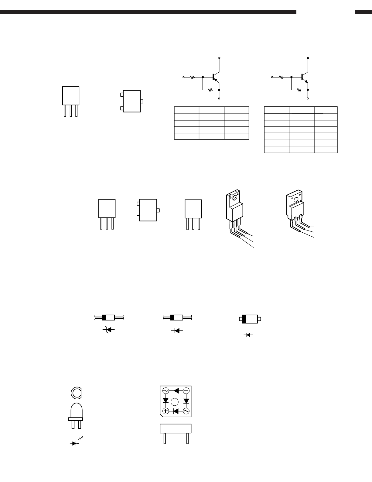
TRANSISTORS
DTA114ES
DTC114TS
DTC114YS
DTC144ES
FRONT
VIEW
C
B
E
DTA114EK
DTA114YK
DTA144EK
DTC114EK
DTC114YK
DTC144EK
B
TOP
C
VIEW
E
DTA Series
R1
B
DTA114EK
DTA114ES
DTA114YK
DTA144EK
10kohm
10kohm /Ω10kohm
10kohm
47kohm
R2
R1
E
Ω
/
/
Ω
/
Ω
C
10kohm
47kohm
47kohm
R2
AVR-1603/683
DTC Series
C
R1
B
R2
E
R1
Ω
/
/Ω
/
Ω
/
Ω
DTC114EK
DTC114TS
DTC114YK
DTC114YS
DTC144EK
DTC144ES
10kohm
10kohm
10kohm /Ω47kohm
10kohm /Ω47kohm
47kohm
47kohm
R2
Ω
10kohm
/
/
Ω
47kohm
/
Ω
47kohm
/
Ω
Ω
/
/Ω
/Ω
/
Ω
/
Ω
2SC1740S
2SC3199Y
KSA916Y
KSA992F
KSC1845F
KTA1266Y
FRONT
VIEW
KTA1268BL
KTC2874B
C
KTC3198Y
E
KTC3200BL
DIODES (LED included)
MTZJ5.1B
MTZJ6.8B
MTZJ7.5A
MTZJ8.2B
MTZJ11B
MTZJ18B
MTZJ20B
2SC2412K
2SK117
KTC3880S
B
TOP
C
VIEW
E
B
FRONT
VIEW
G
D
S
1N4007
2SD947F 2SD3290Y
2SB1560Y
E (Emitter)
C (Collector)
B (Base)
KDS160MTZJ3.3B
E (Emitter)
C (Collector)
B (Base)
1SS133
TOP VIEW
HL-50RDRF4T
TOP VIEW
KBPC604
TOP VIEW
20
Page 21
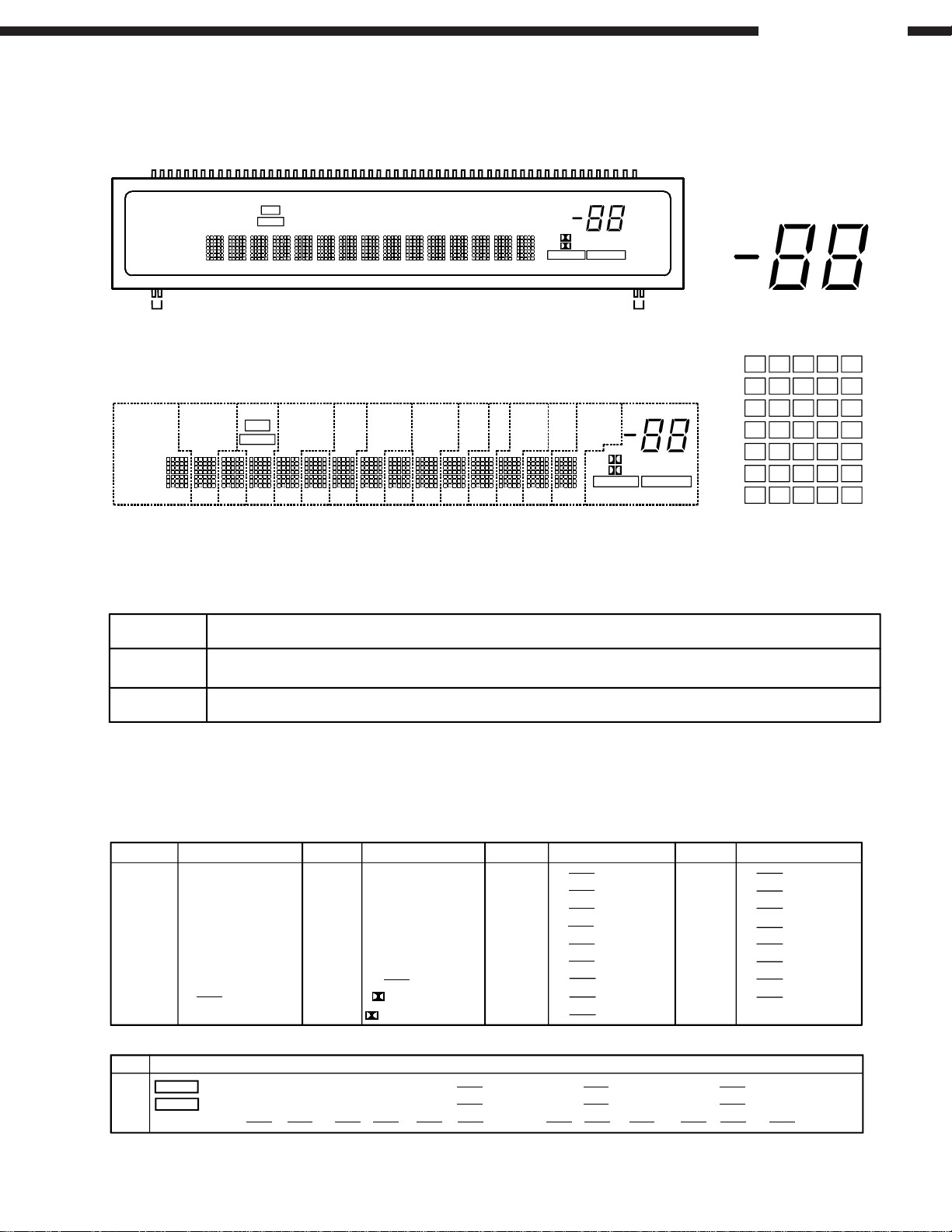
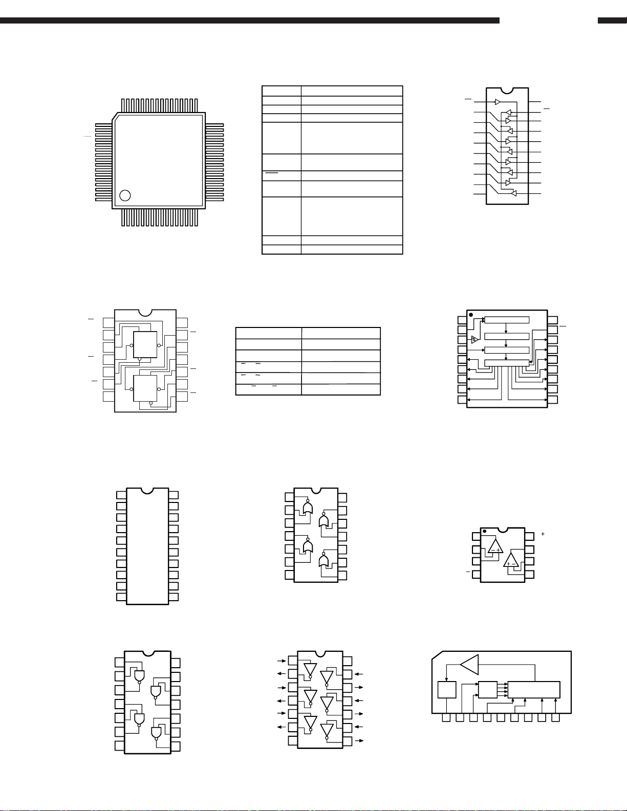
FL DISPLAY
16-st-42GNK (FL301)
AVR-1603/683
1
TUNED
STEREO
RDS
CH
G16
TUNED
RDS
CH
G15 G13
STEREO
AUTO
Pin Assignment
AUTO
G14
MULTI
REC
MULTI
REC
PHONO
VCR
G12
PHONO
VCR
G11
CD
1
−
G10
CD
−
1
TUNER
−2−
3 V.AUX
G9
TUNER
3
−2−
G8
AUXMDDVD /
G7
AUX
V.AUX
VDP TV
TAPE
/
G6
DVD /
MD
G5
/
−1−
G4
VDP
TAPE
/
2
DBS
DIGITAL
G3
TV
−1−
PRO LOGIC
DIGITAL
ANALOG
G2
/ DBS
2
DIGITAL
58
F2F1
G1
PRO LOGIC
DIGITAL
ANALOG
S38
S1
S6
S11
S16
S21
S26
S31
S14
S13
S9
S10
S15
S11
S12
G2~G16
S3
S2
S7
S8
S13
S12
S18
S17
S23
S22
S28
S27
S33
S32
G1
S9
S14
S19
S24
S29
S34
S1
S6
S2
S7
S5
S3
S4
S4
S5
S10
S15
S20
S25
S30
S35
PIN NO.
CONNECTION
PIN NO.
CONNECTION
PIN NO.
CONNECTION
12345
F1 F1 S1 S2 S3
21 22
23 24 25
S19 S20 S21 S22 S23 S24 S25 S26 S27 S28 S29 S30 S31 S32 S33 S34 S35 S36 S37 S38
41 42 43 44 45
G16 G15 G14 G13 G12 G11 G10 G9 G8 G7 G6 G5 G4 G3 G2 G1 F2 F2
Anode & Grid Assignment
G1
G2~G16
S1
S2
S3
S4
S5
S6
S7
S8
S9
TV
VDP
−
2
1
TAPE
S36
S37
S38
S1
S2
S3
S4
S5
S6
S7
S1
S2
S3
S4
S5
S6
S7
S8
S9
S9
G1 G2 G3 G4 G5 G6 G7 G8 G9 G10 G11 G12 G13 G14 G15 G16
DIGITAL
ANALOG
S38
/
−
DBS
S10
S11
S12
S13
S14
S15
S16
S17
S18
/(DVD)
/(MD)
6
S4
26
46
G1
S10
S11
S12
S13
S14
S15
DIGITAL
PRO LOGIC
DVD
MD
V.AUX
7 8 9 10111213141516171819
S5 S6 S7 S8 S9 S10 S11 S12 S13 S14 S15 S16 S17
27 28 29 30 31 32 33 34
47 48 49 50 51 52 53 54 55 56 57
35 36 37 38 39 40
58
F1, F2 : Filament
G1~G16 : Grid
S1~S38 : Anode
G2~G16
S13
S14
S15
S16
S17
S18
AUX
S10
S11
S12
S19
S20
S21
S22
S23
S24
S25
S26
S27
TUNER
−
2
−
3
CD
−
G1
G2~G16
S19
S20
S21
S22
S23
S24
S25
S26
S28
S29
S30
S31
S32
S33
S34
S35
S27
PHONO
1
VCR
REC
MULTI
G1
STEREO
AUTO
G2~G16
S28
S29
S30
S31
S32
S33
S34
S35
TUNED
RDS
20
S18
CH
21
Page 22
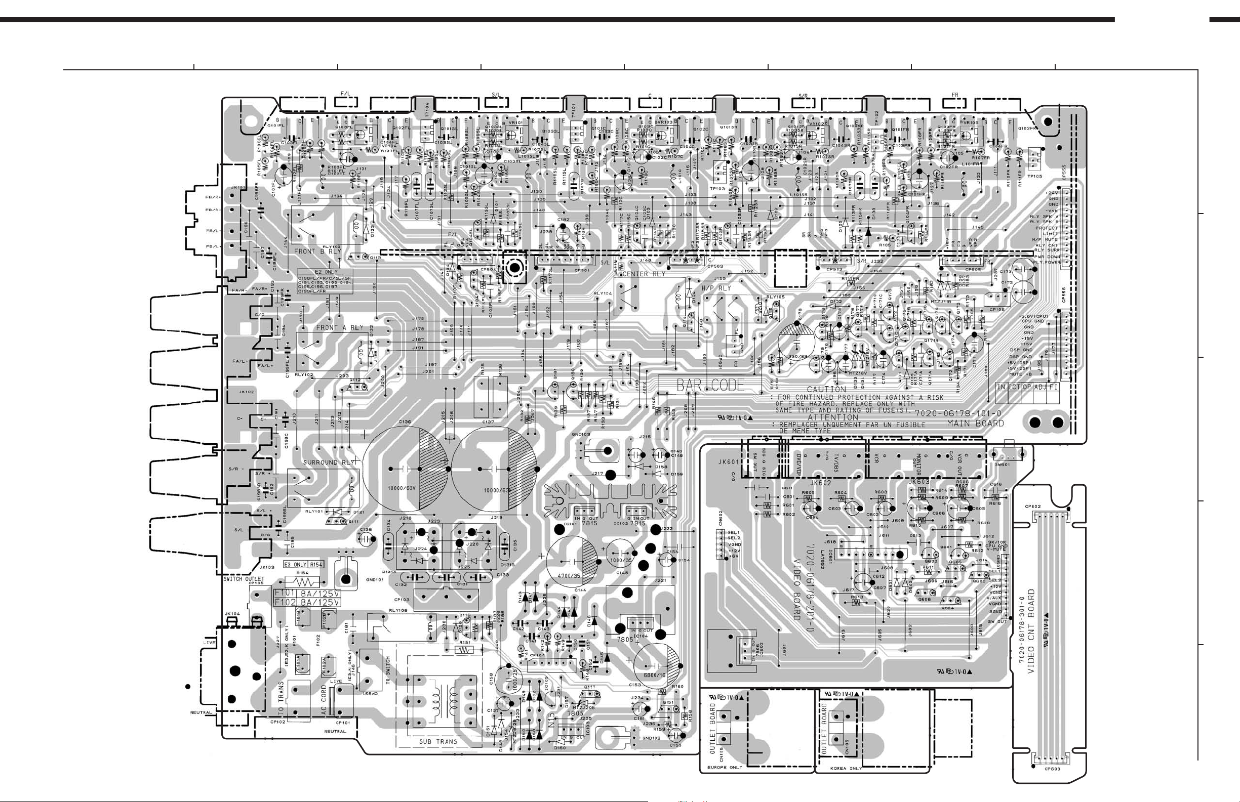
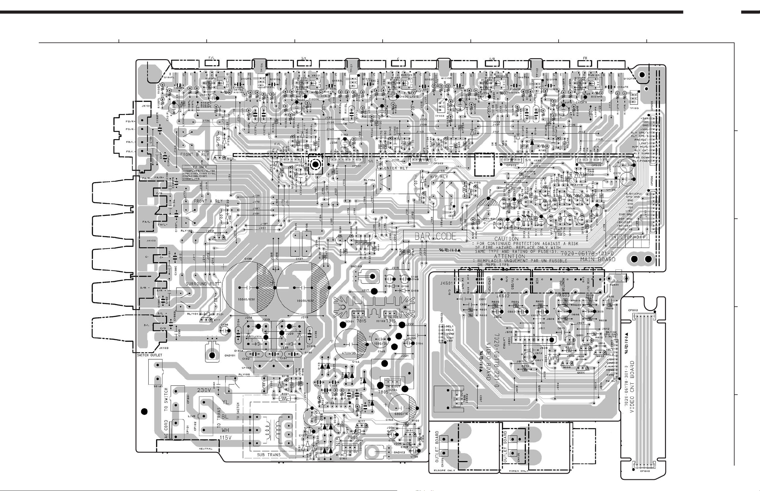
PRINTED WIRING BOARDS
AVR-1603/683
1
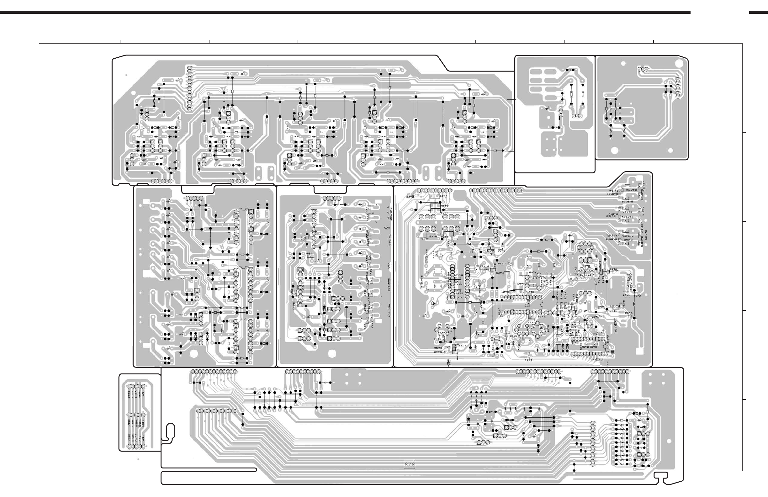
MAIN P.W.B. UNIT(for U.S.A., Canada, U.K., Europe, China, Korea & Australia models)
2
3
4
5
76
8
A
B
C
D
E
COMPONENT SIDE
22
Page 23
AVR-1603/683
1
MAIN P.W.B. UNIT(for Asia, HongKong, & Taiwan R.O.C. models)
2
3
4
5
76
8
A
B
C
D
E
COMPONENT SIDE
23
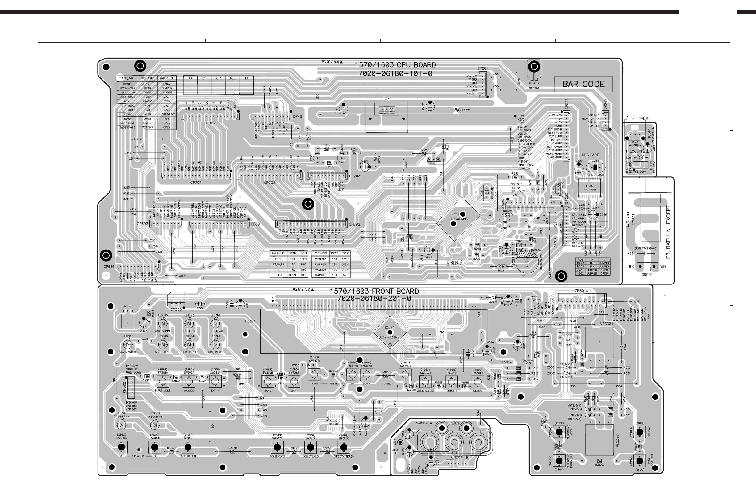
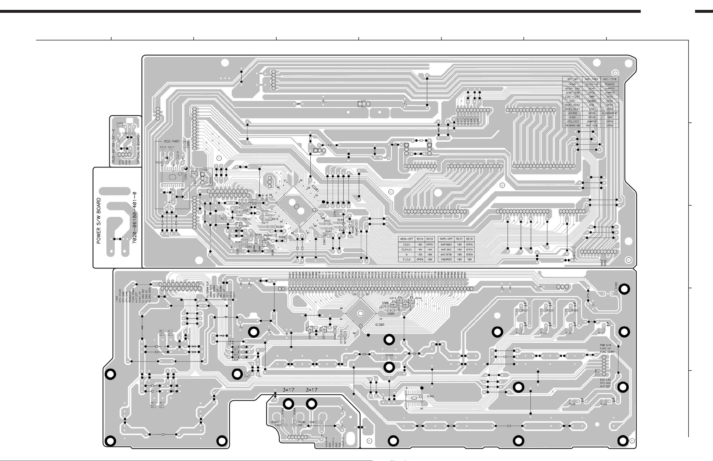
Page 24
AVR-1603/683
1
CPU P.W.B. UNIT
2
3
4
5
76
8
A
B
C
D
E
COMPONENT SIDE
24
Page 25
AVR-1603/683
1
2
3
4
5
76
8
A
B
C
D
E
FOIL SIDE
25
Page 26
AVR-1603/683
1
CNT P.W.B. UNIT
2
3
4
5
76
8
A
B
C
D
E
COMPONENT SIDE
26
Page 27
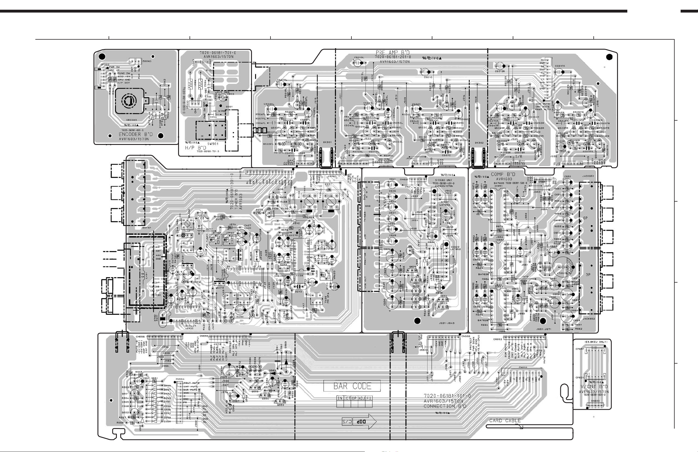
AVR-1603/683
1
2
3
4
5
76
8
A
B
C
D
E
FOIL SIDE
27
Page 28
AVR-1603/683
1
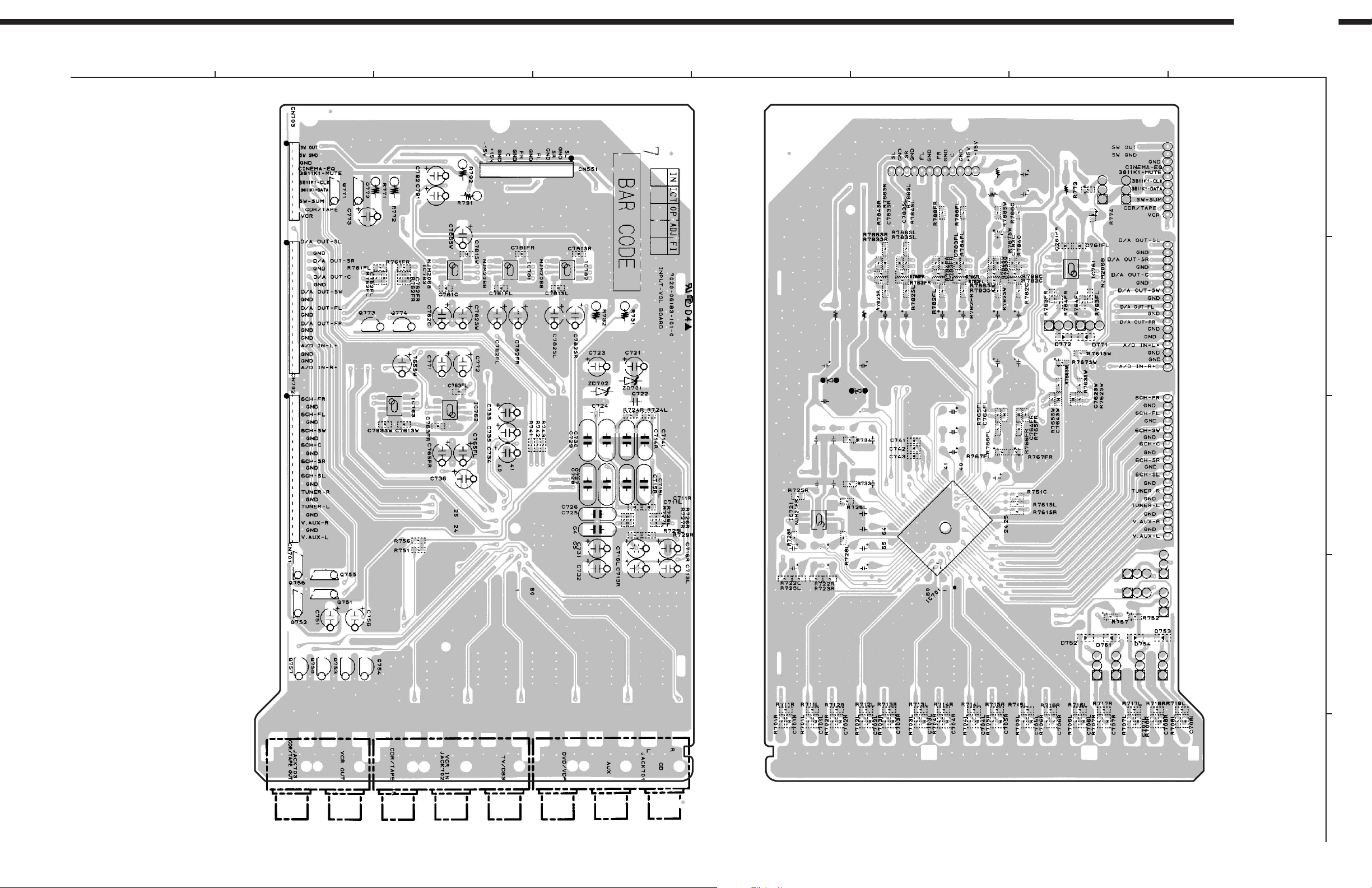
INPUT-VOL P.W.B. UNIT
2
3
4
5
76
8
A
B
C
D
E
COMPONENT SIDE FOIL SIDE
28
Page 29
AVR-1603/683
1
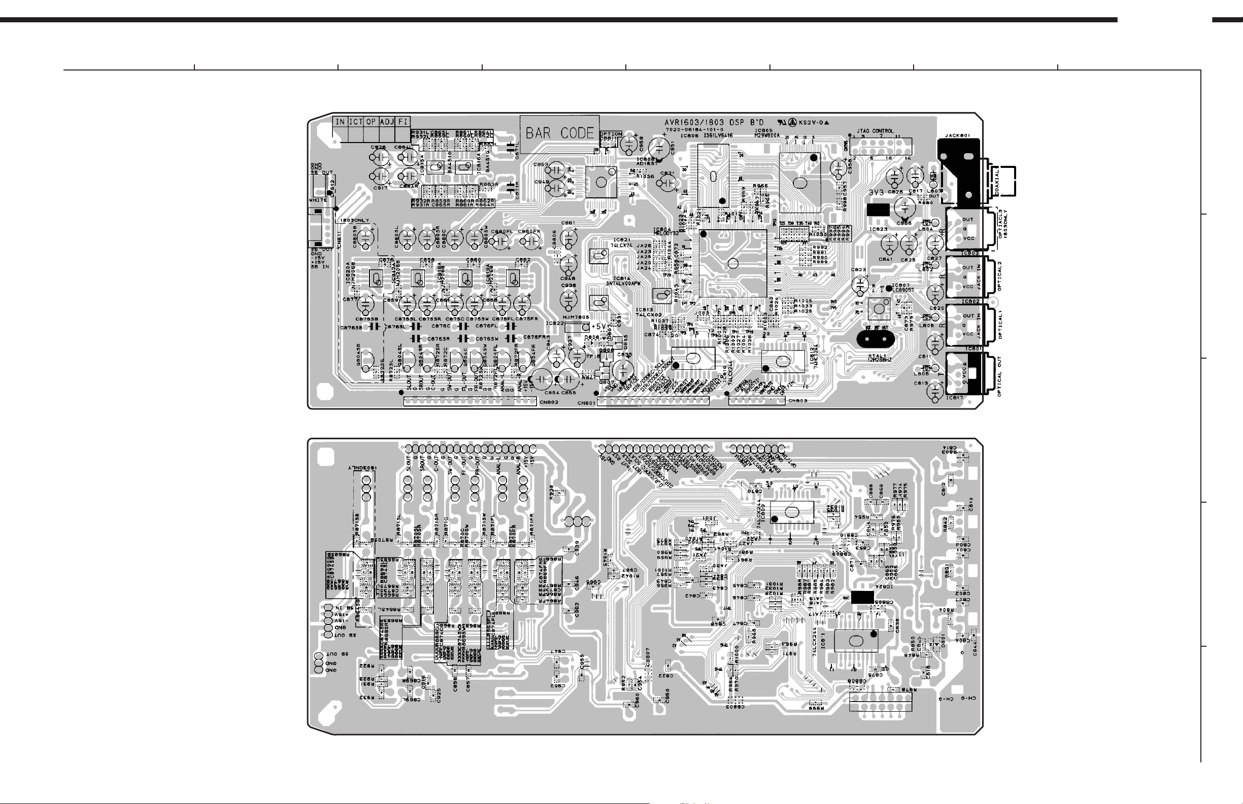
DSP P.W.B. UNIT
2
3
4
5
76
8
A
B
COMPONENT SIDE
C
D
FOIL SIDE
E
29
Page 30
AVR-1603/683
1
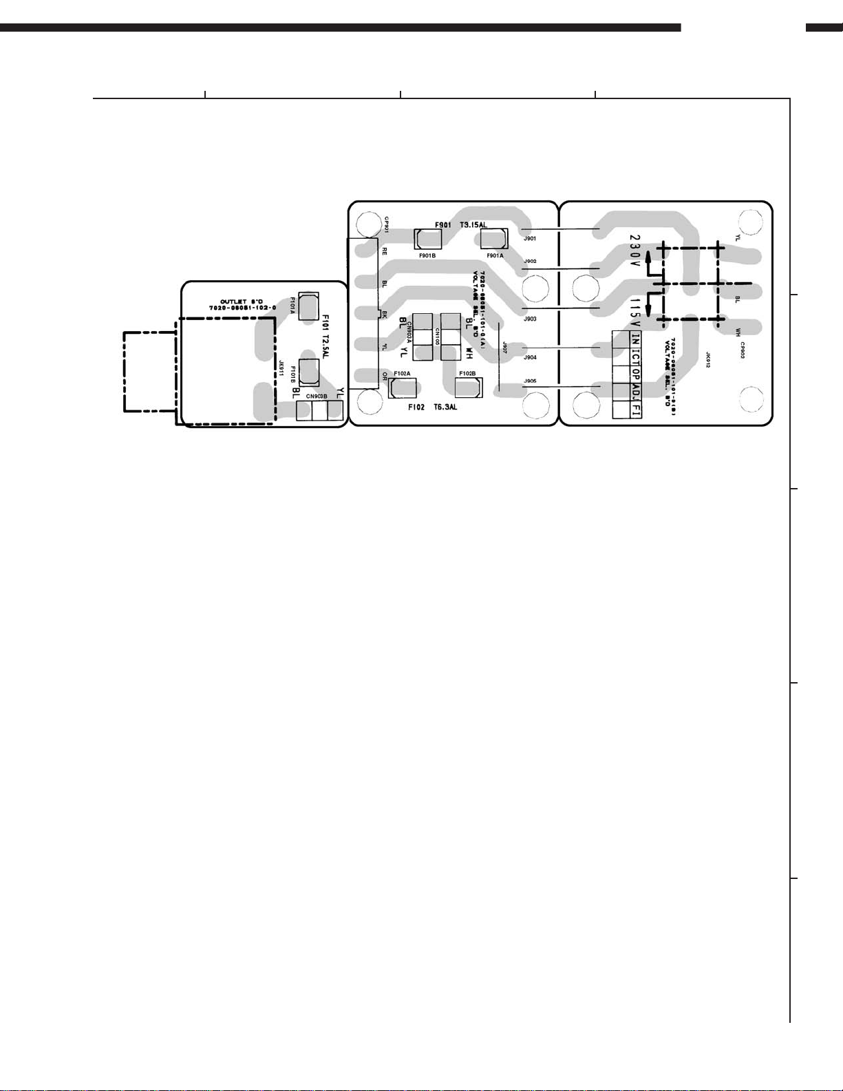
VOLTAGE SEL P.W.B. UNIT
32
4
A
B
COMPONENT SIDE
C
D
E
30
Page 31

NOTE FOR PARTS LIST
l Part indicated with the mark " " are not always in stock and possibly to take a long period of time for supplying, or in
some case supplying of part may be refused.
l When ordering of part, clearly indicate "1" and "I" (i) to avoid mis-supplying.
l Ordering part without stating its part number can not be supplied.
l Part indicated with the mark " " is not illustrated in the exploded view.
l Not including Carbon Film ±5%, 1/4W Type in the P.W.Board parts list. (Refer to the Schematic Diagram for those parts.)
WARNING:
Parts marked with this symbol
Use ONLY replacement parts recommended by the manufacturer.
have critical characteristics.
AVR-1603/683
ll
l Resistors
ll
Ex.: RN 14K 2E 182 G FR
Type Shape Power Resist- Allowable Others
and per- ance error
formance
t
RD : Carbon 2B : 1/8W F :±1% P : Pulse-resistant type
RC : Composition 2E : 1/4W G : ±2% NL : Low noise type
RS : Metal oxide film 2H :1/2W J : ±5% NB : Non-burning type
RW : Winding 3A : 1W K :±10% FR :Fuse-resistor
RN : Metal film 3D : 2W M :±20% F :Lead wire forming
RK : Metal mixture 3F : 3W
t
3H :5W
Resistance
1 8 2 ⇒ 1800 ohm = 1.8 kohm
s
s
• Units: ohm
1 R 2 ⇒ 1.2 ohm
s
s
• Units: ohm
Indicates number of zeros after effective number.
2-digit effective number.
1-digit effective number.
2-digit effective number, decimal point indicated by R.
t
t
ll
l Capacitors
ll
Ex.: CE 04W 1H 2R2 M BP
Type Shape Dielectric Capacity Allowable Others
and per- strength error
formance
t
CE :Aluminum foil 0J : 6.3V F : ±1% HS : High stability type
electrolytic
CA :Aluminum solid 1A : 10V G : ±2% BP : Non-polar type
electrolytic
CS :Tantalum electrolytic 1C : 16V J : ±5% HR: Ripple-resistant type
CQ : Film 1E : 25V K : ±10% DL : For change and discharge
CK :Ceramic 1V : 35V M : ±20% HF : For assuring high
CC :Ceramic 1H :50V Z : +80% U : UL part
CP :Oil 2A : 100V –20% C : CSA part
CM : Mica 2B : 125V P : +100% W : UL-CSA type
CF :Metallized 2C : 160V –0% F : Lead wire forming
CH :Metallized 2D : 200V C : ±0.25pF
t
2E : 250V D : ±0.5pF
2H : 500V = : Others
2J : 630V
t
Capacity (electrolyte only)
2 2 2 ⇒ 2200µF
s
s
• Units: µF.
2 R 2 ⇒ 2.2µF
s
s
• Units: µF.
Indicates number of zeros after effective number.
2-digit effective number.
1-digit effective number.
2-digit effective number, decimal point indicated by R.
Capacity (except electrolyte)
2 2 2 ⇒ 2200pF=0.0022µF
s
s
(More than 2) Indicates number of zeros after effective number.
• Units: pF.
2 2 1 ⇒ 220pF
s
s
(0 or 1) Indicates number of zeros after effective number.
• Units: pF.
• When the dielectric strength is indicated in AC, "AC" is included after the dieelectric
strength value.
2-digit effective number.
2-digit effective number.
t
requency
31
Page 32

AVR-1603/683
Note : The symbols in the column “Remarks” indicate the following destinations.
E3 : U.S.A. & Canada model E1 : Asia model
PARTS LIST OF P.W.B. UNIT ASS'Y
MAIN P.W.B. ASS'Y
Ref. No. Part No. Part Name Remarks Ref. No. Part No. Part Name Remarks
SEMICONDUCTORS GROUP
IC101 963 0057 903 IC KIA7815AP
IC102 963 0021 502 IC KIA7915PI
IC103 960 0159 501 IC KIA7805API
IC104 963 0057 709 IC KIA7805AP
IC105 960 0195 808 IC ICP-N15
IC601 960 0180 101 IC LA7952
IC602 960 0044 108 IC KIA7806AP for E3
Q104C 960 0196 506 Transistor KSC1845F
Q104FL 960 0196 506 Transistor KSC1845F
Q104FR 960 0196 506 Transistor KSC1845F
Q104SL 960 0196 506 Transistor KSC1845F
Q104SR 960 0196 506 Transistor KSC1845F
Q111 960 0196 904 Transistor DTC114YS
Q112 960 0196 904 Transistor DTC114YS
Q113 960 0196 904 Transistor DTC114YS
Q114 960 0196 904 Transistor DTC114YS
Q115 960 0196 904 Transistor DTC114YS
Q116 960 0196 409 Transistor 2SC1740SR
Q117 960 0196 904 Transistor DTC114YS
Q151 960 0196 409 Transistor 2SC1740SR
Q171 960 0005 202 Transistor KTC3198Y
Q171A 960 0196 302 Transistor KTA1268BL
Q171B 960 0196 302 Transistor KTA1268BL
Q171C 960 0196 302 Transistor KTA1268BL
Q172 960 0005 202 Transistor KTC3198Y
Q173 960 0005 202 Transistor KTC3198Y
Q174 960 0005 202 Transistor KTC3198Y
Q175 960 0005 202 Transistor KTC3198Y
Q176 960 0005 202 Transistor KTC3198Y
Q177 960 0005 202 Transistor KTC3198Y
Q178 960 0005 105 Transistor KTA1266Y
Q179 960 0189 005 Transistor KSA916Y
Q180 960 0196 302 Transistor KTA1268BL
Q181 960 0196 302 Transistor KTA1268BL
Q601 960 0005 202 Transistor KTC3198Y
Q602 960 0005 202 Transistor KTC3198Y
Q603 960 0196 904 Transistor DTC114YS
Q604 960 0196 904 Transistor DTC114YS
Q605 960 0196 904 Transistor DTC114YS
Q606 960 0196 904 Transistor DTC114YS
D101 963 0096 508 Diode 1N4148-52RE
D102 963 0096 508 Diode 1N4148-52RE
D103 963 0096 508 Diode 1N4148-52RE
D104 963 0096 508 Diode 1N4148-52RE
D105 963 0096 508 Diode 1N4148-52RE
D121 963 0096 508 Diode 1N4148-52RE
D122 963 0096 508 Diode 1N4148-52RE
EU : U.S.A. model (AVR-683) E1C : China model
E2 : Europe model E1H : Hong Kong model
EK : U.K. model E1T : Taiwan R.O.C. model
EA : Australia model E1K : Korea model
D123 963 0096 508 Diode 1N4148-52RE
D124 963 0096 508 Diode 1N4148-52RE
D125 963 0096 508 Diode 1N4148-52RE
D126 963 0096 508 Diode 1N4148-52RE
D131A 960 0197 107 Diode KBPC604 6A
D131B 960 0197 107 Diode KBPC604 6A
D132 963 0096 508 Diode 1N4148-52RE
D133 963 0046 202 Zener diode MTZJ18B
D134 963 0046 202 Zener diode MTZJ18B
D135 963 0096 508 Diode 1N4148-52RE
D136 963 0058 504 Zener diode MTZJ11B-0.5W
D137 963 0096 508 Diode 1N4148-52RE
D138 963 0058 407 Diode IN4007
D141 963 0058 407 Diode IN4007
D142 963 0058 407 Diode IN4007
D143 963 0058 407 Diode IN4007
D144 963 0058 407 Diode IN4007
D145 963 0058 407 Diode IN4007
D146 963 0058 407 Diode IN4007
D148 963 0096 508 Diode 1N4148-52RE
D149 963 0058 407 Diode IN4007
D150 963 0058 407 Diode IN4007
D151 963 0096 508 Diode 1N4148-52RE
D152 963 0058 407 Diode IN4007
D153 963 0058 407 Diode IN4007
D154 960 0095 908 Zener diode MTZJ8.2B
D157 963 0058 708 Zener diode MTZJ20B
D158 963 0096 508 Diode 1N4148-52RE
D159 963 0096 508 Diode 1N4148-52RE
D160 963 0096 508 Diode 1N4148-52RE
D601 963 0096 508 Diode 1N4148-52RE
D602 963 0096 508 Diode 1N4148-52RE
RESISTORS GROUP
R104C 963 9005 451 Metal oxide 5.6 kohm 1W
R104FL 963 9005 451 Metal oxide 5.6 kohm 1W
R104FR 963 9005 451 Metal oxide 5.6 kohm 1W
R104SL 963 9005 451 Metal oxide 5.6 kohm 1W
R104SR 963 9005 451 Metal oxide 5.6 kohm 1W
R105C 963 9005 451 Metal oxide 5.6 kohm 1W
R105FL 963 9005 451 Metal oxide 5.6 kohm 1W
R105FR 963 9005 451 Metal oxide 5.6 kohm 1W
R105SL 963 9005 451 Metal oxide 5.6 kohm 1W
R105SR 963 9005 451 Metal oxide 5.6 kohm 1W
R106C 963 0047 900 Metal film 4.7 kohm 1W
R106FL 963 0047 900 Metal film 4.7 kohm 1W
R106FR 963 0047 900 Metal film 4.7 kohm 1W
R106SL 963 0047 900 Metal film 4.7 kohm 1W
R106SR 963 0047 900 Metal film 4.7 kohm 1W
R107C 963 0047 900 Metal film 4.7 kohm 1W
R107FL 963 0047 900 Metal film 4.7 kohm 1W
32
Page 33

AVR-1603/683
Ref. No. Part No. Part Name Remarks
R107FR 963 0047 900 Metal film 4.7 kohm 1W
R107SL 963 0047 900 Metal film 4.7 kohm 1W
R107SR 963 0047 900 Metal film 4.7 kohm 1W
R108C 963 9005 477 Metal oxide 0.22 ohm 1W
R108FL 963 9005 477 Metal oxide 0.22 ohm 1W
R108FR 963 9005 477 Metal oxide 0.22 ohm 1W
R108SL 963 9005 477 Metal oxide 0.22 ohm 1W
R108SR 963 9005 477 Metal oxide 0.22 ohm 1W
R109C 963 9005 477 Metal oxide 0.22 ohm 1W
R109FR 963 9005 477 Metal oxide 0.22 ohm 1W
R109FL 963 9005 477 Metal oxide 0.22 ohm 1W
R109SL 963 9005 477 Metal oxide 0.22 ohm 1W
R109SR 963 9005 477 Metal oxide 0.22 ohm 1W
R110C 963 9005 477 Metal oxide 0.22 ohm 1W
R110FR 963 9005 477 Metal oxide 0.22 ohm 1W
R110FL 963 9005 477 Metal oxide 0.22 ohm 1W
R110SL 963 9005 477 Metal oxide 0.22 ohm 1W
R110SR 963 9005 477 Metal oxide 0.22 ohm 1W
R111C 963 9005 477 Metal oxide 0.22 ohm 1W
R111FL 963 9005 477 Metal oxide 0.22 ohm 1W
R111FR 963 9005 477 Metal oxide 0.22 ohm 1W
R111SL 963 9005 477 Metal oxide 0.22 ohm 1W
R111SR 963 9005 477 Metal oxide 0.22 ohm 1W
R118C 963 9005 480 Metal oxide 10 ohm 1W
R118FL 963 9005 480 Metal oxide 10 ohm 1W
R118FR 963 9005 480 Metal oxide 10 ohm 1W
R118SL 963 9005 480 Metal oxide 10 ohm 1W
R118SR 963 9005 480 Metal oxide 10 ohm 1W
R119C 963 9005 480 Metal oxide 10 ohm 1W
R119FL 963 9005 480 Metal oxide 10 ohm 1W
R119FR 963 9005 480 Metal oxide 10 ohm 1W
R119SL 963 9005 480 Metal oxide 10 ohm 1W
R119SR 963 9005 480 Metal oxide 10 ohm 1W
R135 963 0045 203 Winding 0.1 ohm 5W
R136 963 0045 203 Winding 0.1 ohm 5W
R141 960 0180 606 Metal film 0.22 ohm 1W
R142 960 0180 606 Metal film 0.22 ohm 1W
R148 960 0180 606 Metal film 0.22 ohm 1W
R149 960 0180 606 Metal film 0.22 ohm 1W
R151 963 9003 343 Metal film 68 ohm 1/4W
R154 963 0043 108 Metal film 2.2 Mohm 2W for E3,EU
R179 963 9003 055 Metal film 47 kohm 1/4W
R181 963 0047 900 Metal film 4.7 kohm 1W
R185 963 9005 655 Metal film 22 ohm 1/4W
VR101 960 0091 601 Semi fixed resistor 1kohm
VR102 960 0091 601 Semi fixed resistor 1kohm
VR103 960 0091 601 Semi fixed resistor 1kohm
VR104 960 0091 601 Semi fixed resistor 1kohm
VR105 960 0091 601 Semi fixed resistor 1kohm
Ref. No. Part No. Part Name Remarks
CAPACITORS GROUP
C101C 093 9005 888 Electrolytic 47uF/50V
C101FL 093 9005 888 Electrolytic 47uF/50V
C101FR 093 9005 888 Electrolytic 47uF/50V
C101SL 093 9005 888 Electrolytic 47uF/50V
C101SR 093 9005 888 Electrolytic 47uF/50V
C102C 963 9005 752 Electrolytic 10uF/35V
C102FL 963 9005 752 Electrolytic 10uF/35V
C102FR 963 9005 752 Electrolytic 10uF/35V
C102SL 963 9005 752 Electrolytic 10uF/35V
C102SR 963 9005 752 Electrolytic 10uF/35V
C103C 963 9003 084 Ceramic 100pF/500V
C103FL 963 9003 084 Ceramic 100pF/500V
C103FR 963 9003 084 Ceramic 100pF/500V
C103SL 963 9003 084 Ceramic 100pF/500V
C103SR 963 9003 084 Ceramic 100pF/500V
C104C 963 9003 084 Ceramic 100pF/500V
C104FL 963 9003 084 Ceramic 100pF/500V
C104FR 963 9003 084 Ceramic 100pF/500V
C104SL 963 9003 084 Ceramic 100pF/500V
C104SR 963 9003 084 Ceramic 100pF/500V
C105C 960 9003 108 Ceramic 0.022uF/25V
C105FL 960 9003 108 Ceramic 0.022uF/25V
C105FR 960 9003 108 Ceramic 0.022uF/25V
C105SL 960 9003 108 Ceramic 0.022uF/25V
C105SR 960 9003 108 Ceramic 0.022uF/25V
C107C 963 9003 097 Mylar film 0.1uF/250V
C107FL 963 9003 097 Mylar film 0.1uF/250V
C107FR 963 9003 097 Mylar film 0.1uF/250V
C107SL 963 9003 097 Mylar film 0.1uF/250V
C107SR 963 9003 097 Mylar film 0.1uF/250V
C131 963 9003 097 Mylar film 0.1uF/250V
C132 963 9003 097 Mylar film 0.1uF/250V
C133 963 9003 097 Mylar film 0.1uF/250V
C134 963 9003 097 Mylar film 0.1uF/250V
C135 963 9003 097 Mylar film 0.1uF/250V
C136 963 0087 203 Electrolytic 10000uF/63V
C137 963 0087 203 Electrolytic 10000uF/63V
C138 963 9005 749 Electrolytic 1uF/50V
C141 963 0021 900 Mylar film 0.047uF/100V
C142 963 0021 900 Mylar film 0.047uF/100V
C143 963 0021 900 Mylar film 0.047uF/100V
C144 963 9003 110 Electrolytic 4700uF/35V
C145 963 9003 123 Electrolytic 1000uF/35V
C146 963 9005 749 Electrolytic 1uF/50V
C148 963 9005 749 Electrolytic 1uF/50V
C150 963 0021 900 Mylar film 0.047uF/100V
C151 963 0021 900 Mylar film 0.047uF/100V
C152 963 0021 900 Mylar film 0.047uF/100V
C153 963 0021 104 Electrolytic 6800uF/16V
C154 963 9005 752 Electrolytic 10uF/35V
C155 963 0020 202 Ceramic 0.1uF/50V
33
Page 34

AVR-1603/683
Ref. No. Part No. Part Name Remarks New
C157 963 9005 749 Electrolytic 1uF/50V
C158 963 9003 136 Electrolytic 1000uF/25V
C159 963 9005 749 Electrolytic 1uF/50V
C161 963 9005 752 Electrolytic 10uF/35V
C171 963 9005 312 Electrolytic 100uF/10V
C171A 963 0020 202 Ceramic 0.1uF/50V
C171B 963 0020 202 Ceramic 0.1uF/50V
C171C 963 0020 202 Ceramic 0.1uF/50V
C172 963 9005 833 Electrolytic 220uF/6.3V
C173 963 9005 833 Electrolytic 220uF/6.3V
C174 963 9005 752 Electrolytic 10uF/35V
C175 963 9005 914 Electrolytic 4.7uF/50V
C176 963 9005 749 Electrolytic 1uF/50V
C177 963 9005 749 Electrolytic 1uF/50V
C178 963 9003 149 Electrolytic 330uF/63V
C181 963 0076 104 Ceramic 0.047uF/250V(AC) for E2,EK,EA
C182 963 9004 795 Electrolytic 10uF/100V
C191 963 9006 007 Ceramic 2200pF/16V for E2,EK,EA *
C192 963 9006 007 Ceramic 2200pF/16V for E2,EK,EA *
C193 963 9006 007 Ceramic 2200pF/16V for E2,EK,EA *
C194 963 9006 007 Ceramic 2200pF/16V for E2,EK,EA *
C195 963 9006 007 Ceramic 2200pF/16V for E2,EK,EA *
C196 963 9006 007 Ceramic 2200pF/16V for E2,EK,EA *
C197 963 9006 007 Ceramic 2200pF/16V for E2,EK,EA *
C198C 960 9006 202 Ceramic 0.01uF/50V for E2,EK,EA
C198FL 960 9006 202 Ceramic 0.01uF/50V for E2,EK,EA
C198FR 960 9006 202 Ceramic 0.01uF/50V for E2,EK,EA
C198SL 960 9006 202 Ceramic 0.01uF/50V for E2,EK,EA
C198SR 960 9006 202 Ceramic 0.01uF/50V for E2,EK,EA
C199FL 960 9006 202 Ceramic 0.01uF/50V for E2,EK,EA
C199FR 960 9006 202 Ceramic 0.01uF/50V for E2,EK,EA
Ref. No. Part No. Part Name Remarks
OTHER PARTS GROUP
CN601 963 0086 709 11P connector socket 1
CN602 963 0085 603 5P connector socket 1
CP101 960 0118 908 AC cord connector base 1
CP102 960 0128 901 3P connector base for E3,EU,E2,
960 0128 901 3P connector base
CP103 960 0128 901 3P connector base 1
CP104 960 0128 804 6P connector base 1
CP105 960 0123 304 3P connector base for E2,E1,
CP106 960 0123 207 3P connector base 1
CP501 963 0086 806 9P connector base 1
CP502-504 963 0086 903 5P connector base 3
CP505 963 0087 009 6P connector base 1
CP555 960 0239 609 13P connector base 1
CP556 963 0087 805 11P connector base 1
CP602,603 963 0086 903 5P connector base 2
CP901 963 0048 909 3P connector base 1
CP931 960 0123 304 3P connector base
F101,102 960 0188 705 Fuse 125V-S8A for E3,EU 2
F101 960 0142 602 Fuse 250V-S2.5A
F102 963 0044 709 Fuse 250V-S3.15A for E2,E1C,
F101A,102A
F101B,102B
F102A,F102B
GND101-103
960 0005 804 Fuse clip holder 2
960 0005 804 Fuse clip holder 2
960 0005 804 Fuse clip holder for E1C 2
960 9006 600 Terminal 3
E1C,E1K,EK,EA
for E1,E1H,E1T
E1H,E1K,E1T 1
for E2,E1,E1C,
E1K,E1H,E1T 1
for E2,E1K,EK,EA
E1K,EK,EA 1
Q'ty New
1
1
1
C601 963 9004 520 Ceramic 100pF/50V
C602 963 9005 309 Electrolytic 47uF/10V
C603 963 9005 309 Electrolytic 47uF/10V
C604 963 9005 309 Electrolytic 47uF/10V
C605 963 9005 891 Electrolytic 470uF/6.3V
C606 963 9005 891 Electrolytic 470uF/6.3V
C607 963 9005 794 Electrolytic 100uF/16V
C611 963 9004 546 Ceramic 0.01uF/16V
C612 963 9004 562 Ceramic 0.047uF/50V
C613 963 9004 562 Ceramic 0.047uF/50V
JK103 960 0194 809 2P speaker terminal 1
JK104 960 0187 803 AC outlet(2P) for E3,EU 1
960 0143 203 AC outlet for E2,EK,EA 1
L101C,FL,
FR,SL,SR 963 0049 005 Inductor 0.5uh 5
RLY101-104
RLY105 963 0071 303 Relay RSB24S 1
RLY106 960 0181 605 Relay G5PA-1-8 1
TP101-105 960 0161 405 3P connector base 1
960 0181 702 Relay G5PA-2 4
963 0076 104 Ceramic 0.047uf/250V(AC) 1
960 0158 308 SW Push block 1
963 0074 009 8P Speaker terminal 1
960 0194 508 1P Pin jack 1
960 0194 605 2P Pin jack 1
960 0188 404 3P Pin jack 1
Heat sink reg TR 1 *
34
Page 35

Ref. No. Part No. Part Name Remarks
Heat sink reg TR 1 *
Heat sink 1 *
963 0094 924 Mini trans for E3 1 *
963 0094 937 Mini trans for E2,EK,EA 1 *
963 0094 911 Mini trans for E1C 1 *
963 0094 940 Mini trans for E1H 1 *
963 0094 911 Mini trans for E1K 1 *
963 0094 940 Mini trans for E1T 1 *
963 0094 940 Mini trans for E1 1 *
963 0094 924 Mini trans for EU 1 *
963 0018 007 Screw 3x8 B-type ZNY/BH 1
963 0018 007 Screw 3x8 B-type ZNY/BH 1
CPU P.W.B. ASS'Y
Q'ty New
Ref. No. Part No. Part Name Remarks
SEMICONDUCTORS GROUP
IC201 963 0095 800 IC CXP740096-156Q
IC202 963 0057 602 IC TDA7330BD
IC271 960 0222 506 IC KIA7812AP
IC301 960 0180 004 IC LC75721E
IC302 963 0074 504 IC BU2090F
IC391 963 0084 905 IC GP1FA502RZ
Q201 963 0075 202 Transistor DTC144EK
Q202 963 0045 902
Q251 963 0075 309 Transistor DTA114ES
Q252 960 0196 603 Transistor KTC2874B
Q253 960 0196 603 Transistor KTC2874B
Q310 963 0058 203 Transistor DTA114EK
Q311 963 0058 203 Transistor DTC114EK
Q312 963 0058 203 Transistor DTA114EK
Q313 963 0058 203 Transistor DTC114EK
Q314 963 0058 203 Transistor DTA114EK
Q315 963 0058 203 Transistor DTC114EK
AVR-1603/683
Transistor 2SC2412KT96(BR)
D201 963 0096 605 Diode 1N4148WS
D202 963 0058 407 Diode IN4007
D203 963 0096 508 Diode 1N4148-52RE
D204 963 0096 605 Diode 1N4148WS
D205 963 0096 605 Diode 1N4148WS
D206 963 0096 508 Diode 1N4148-52RE for E2,EK,EA
D251 963 0058 407 Diode IN4007
D302 963 0096 508 Diode 1N4148-52RE
D303 963 0096 508 Diode 1N4148-52RE
D304 963 0096 508 Diode 1N4148-52RE
D305 963 0096 605 Diode 1N4148WS
D308 963 0096 605 Diode 1N4148WS
D309 963 0096 605 Diode 1N4148WS
ZD201 963 0047 502 Zener diode MTZJ3.3B
ZD301 960 0095 802 Zener diode MTZJ6.8B
ZD331 960 0095 500 Zener diode MTZJ5.1B
ZD332 960 0095 500 Zener diode MTZJ5.1B
ZD335 960 0095 500 Zener diode MTZJ5.1B
ZD336 960 0095 500 Zener diode MTZJ5.1B
LED301-304
LED306-309
960 0197 204 LED HL50RDRF4T
960 0197 204 LED HL50RDRF4T
35
Page 36

AVR-1603/683
Ref. No. Part No. Part Name Remarks Ref. No. Part No. Part Name Remarks
RESISTORS GROUP
R202 963 9003 398 Carbon chip 1 kohm 1/16W
R203 963 9004 342 Carbon chip 4.7 kohm 1/16W
R204 963 9004 342 Carbon chip 4.7 kohm 1/16W
R205 963 9004 070 Carbon chip 10 kohm 1/16W
R206 963 9004 232 Carbon chip 220 kohm 1/16W
R209 963 9004 083 Carbon chip 100 kohm 1/16W
R211 963 9004 070 Carbon chip 10 kohm 1/16W
R212 963 9003 398 Carbon chip 1 kohm 1/16W
R213 963 9004 122 Carbon chip 12 kohm 1/16W
R214 963 9004 122 Carbon chip 12 kohm 1/16W
R215 963 9004 122 Carbon chip 12 kohm 1/16W
R216 963 9004 070 Carbon chip 10 kohm 1/16W for E3,E2,EK,EA,EU
R217 963 9004 070 Carbon chip 10 kohm 1/16W
R218 963 9004 177 Carbon chip 18 kohm 1/16W for E2,EK,EA
963 9004 070 Carbon chip 10 kohm 1/16W
R219 963 9004 177 Carbon chip 18 kohm 1/16W for E2,EK,EA
R220 963 9004 070 Carbon chip 10 kohm 1/16W
R225 963 9004 245 Carbon chip 2.2 Mohm 1/16W for E2,EK,EA
R241 963 9004 339 Carbon chip 470 ohm 1/16W
R242 963 9004 339 Carbon chip 470 ohm 1/16W
R243 963 9004 339 Carbon chip 470 ohm 1/16W
R244 963 9004 339 Carbon chip 470 ohm 1/16W
R245 963 9004 339 Carbon chip 470 ohm 1/16W
R246 963 9004 339 Carbon chip 470 ohm 1/16W
R271 963 9005 626 Metal oxide 4.7 ohm 1W
R281 963 9004 070 Carbon chip 10 kohm 1/16W
R282 963 9004 070 Carbon chip 10 kohm 1/16W
R283 963 9004 070 Carbon chip 10 kohm 1/16W
R305B 963 9004 847 Carbon chip 3.3 kohm 1/16W
R312 963 9004 070 Carbon chip 10 kohm 1/16W
R315 963 0075 105 Carbon chip 10 kohm 1/16W
R321 963 9004 436 Carbon chip 680 ohm 1/16W
R322 963 9004 436 Carbon chip 680 ohm 1/16W
R323 963 9004 436 Carbon chip 680 ohm 1/16W
R324 963 9004 436 Carbon chip 680 ohm 1/16W
R326 963 9004 436 Carbon chip 680 ohm 1/16W
R327 963 9004 436 Carbon chip 680 ohm 1/16W
R328 963 9004 436 Carbon chip 680 ohm 1/16W
R329 963 9004 436 Carbon chip 680 ohm 1/16W
R381 963 9004 465 Carbon chip 75 ohm 1/16W
R382 963 9004 339 Carbon chip 470 ohm 1/16W
R383 963 9004 339 Carbon chip 470 ohm 1/16W
R384 963 9004 245 Carbon chip 2.2 Mohm 1/16W
R385 963 9004 245 Carbon chip 2.2 Mohm 1/16W
RG01 963 9004 397 Carbon chip 56 kohm 1/16W
RP02 963 9004 397 Carbon chip 56 kohm 1/16W
RP03 963 9004 397 Carbon chip 56 kohm 1/16W
RP04 963 9004 397 Carbon chip 56 kohm 1/16W
RP05 963 9004 397 Carbon chip 56 kohm 1/16W
for E1,E1C,E1H,E1K,E1T
RP06 963 9004 397 Carbon chip 56 kohm 1/16W
RP07 963 9004 397 Carbon chip 56 kohm 1/16W
RP08 963 9004 397 Carbon chip 56 kohm 1/16W
RP09 963 9004 397 Carbon chip 56 kohm 1/16W
RP10 963 9004 397 Carbon chip 56 kohm 1/16W
RP11 963 9004 397 Carbon chip 56 kohm 1/16W
RP12 963 9004 397 Carbon chip 56 kohm 1/16W
RP13 963 9004 397 Carbon chip 56 kohm 1/16W
RP14 963 9004 397 Carbon chip 56 kohm 1/16W
RP15 963 9004 397 Carbon chip 56 kohm 1/16W
RP16 963 9004 397 Carbon chip 56 kohm 1/16W
RP17 963 9004 397 Carbon chip 56 kohm 1/16W
RP18 963 9004 397 Carbon chip 56 kohm 1/16W
RP19 963 9004 397 Carbon chip 56 kohm 1/16W
RP20 963 9004 397 Carbon chip 56 kohm 1/16W
RP21 963 9004 397 Carbon chip 56 kohm 1/16W
RP22 963 9004 397 Carbon chip 56 kohm 1/16W
RP23 963 9004 397 Carbon chip 56 kohm 1/16W
RP24 963 9004 397 Carbon chip 56 kohm 1/16W
RP25 963 9004 397 Carbon chip 56 kohm 1/16W
RP26 963 9004 397 Carbon chip 56 kohm 1/16W
RP27 963 9004 397 Carbon chip 56 kohm 1/16W
RP28 963 9004 397 Carbon chip 56 kohm 1/16W
RP29 963 9004 397 Carbon chip 56 kohm 1/16W
RP30 963 9004 397 Carbon chip 56 kohm 1/16W
RP31 963 9004 397 Carbon chip 56 kohm 1/16W
RP32 963 9004 397 Carbon chip 56 kohm 1/16W
RP33 963 9004 397 Carbon chip 56 kohm 1/16W
RP34 963 9004 397 Carbon chip 56 kohm 1/16W
RP35 963 9004 397 Carbon chip 56 kohm 1/16W
RP36 963 9004 397 Carbon chip 56 kohm 1/16W
RP37 963 9004 397 Carbon chip 56 kohm 1/16W
RP38 963 9004 397 Carbon chip 56 kohm 1/16W
CAPACITORS GROUP
BC201 963 0061 504 Electrolytic 8200uF/5.5V
C201 963 9004 698 Ceramic chip 0.01uF/50V
C202 963 9004 711 Ceramic chip 0.1uF/50V
C203 963 9004 698 Ceramic chip 0.01uF/50V
C204 963 9005 914 Electrolytic 4.7uF/50V
C205 963 9004 711 Ceramic chip 0.1uF/50V
C206 096 3905 309 Electrolytic 47uF/10V for E2,EK,EA
C207 963 9004 546 Ceramic 0.01uF/16V for E2,EK,EA
C208 963 9005 354 Ceramic chip 270pF/50V for E2,EK,EA
C209 963 9005 752 Electrolytic 10uF/35V for E2,EK,EA
C210 963 9004 698 Ceramic chip 0.01uF/50V for E2,EK,EA
C211 963 9004 614 Ceramic chip 27pF/50V for E2,EK,EA
C212 963 9004 614 Ceramic chip 27pF/50V for E2,EK,EA
C221 963 9005 312 Electrolytic 100uF/10V
C251 963 9005 927 Electrolytic 0.1uF/50V
C261 963 9004 575 Ceramic chip 100pF/50V
36
Page 37

AVR-1603/683
Ref. No. Part No. Part Name Remarks Ref. No. Part No. Part Name Remarks Q'ty
C262 963 9004 575 Ceramic chip 100pF/50V
C263 963 9004 575 Ceramic chip 100pF/50V
C264 963 9004 575 Ceramic chip 100pF/50V
C265 963 9004 575 Ceramic chip 100pF/50V
C266 963 9004 575 Ceramic chip 100pF/50V
C267 963 9004 575 Ceramic chip 100pF/50V
C271 963 9005 794 Electrolytic 100uF/16V
C272 963 9005 752 Electrolytic 10uF/35V
OTHER PARTS GROUP
BD201,202 963 0053 800 Beads inductor 2
CN201 963 0096 906 6P wire 1
CN202 963 0099 408 4P wire 1
CN302 963 0096 702 6P wire 1
CN931 963 0089 502 2P wire
for E2,E1,G1C,G1H,
G1K,G1T,EK,EA 1
C301 963 9005 778 Electrolytic 10uF/50V
C302 963 9004 753 Ceramic chip 0.047uF/50V
C303 963 9005 309 Electrolytic 47uF/10V
C304 960 9003 108 Ceramic 0.022uF/25V
C305 963 9005 859 Electrolytic 47uF/16V
C306 963 9004 766 Mylar film 0.1uF/100V
C307 963 9005 749 Electrolytic 1uF/50V
C308 963 0021 900 Mylar film 0.047uF/100V
C309 963 0021 900 Mylar film 0.047uF/100V
C310 963 9005 749 Electrolytic 1uF/50V
C311 963 9005 406 Ceramic chip 30pF/50V
C312 963 9005 859 Electrolytic 47uF/16V
C313 963 9005 419 Mylar film 0.047uF/63V
C321 963 9004 685 Ceramic chip 1000pF/50V
C322 963 9004 575 Ceramic chip 100pF/50V
C324 963 9004 575 Ceramic chip 100pF/50V
C325 963 9004 575 Ceramic chip 100pF/50V
C331 963 9004 698 Ceramic chip 0.01uF/50V
C332 963 9004 698 Ceramic chip 0.01uF/50V
C335 963 9004 698 Ceramic chip 0.01uF/50V
C336 963 9004 698 Ceramic chip 0.01uF/50V
C381 963 9005 309 Electrolytic 47uF/10V
C382 963 9004 575 Ceramic chip 100pF/50V
C383 963 9004 575 Ceramic chip 100pF/50V
C384 963 9005 749 Electrolytic 1uF/50V
C385 963 9005 749 Electrolytic 1uF/50V
C386 963 9004 753 Ceramic chip 0.047uF/50V
C391 963 9004 591 Ceramic chip 22pF/50V
C392 963 9004 711 Ceramic chip 0.1uF/50V
C393 963 9005 859 Electrolytic 47uF/16V
C931 963 0076 104 Ceramic 0.047uF/250V(AC)
CP201 963 0097 604 6P connector base 1
CP202 963 0050 104 4P connector base 1
CP301A 963 0097 905 20P connector base 1
CP301B 960 0129 007 20P FFC connector base 1
CP303 963 0049 102 3P connector base 1
CP401 963 0088 008 10P connector base 1
CP402 963 0097 507 15P connector base 1
CP552 960 0239 609 13P connector base 1
CP553 963 0088 008 10P connector base 1
CP601 963 0087 805 11P connector base 1
CP701 963 0087 504 19P connector base 1
CP702 963 0087 902 17P connector base 1
CP703 963 0088 008 10P connector base 1
CP801 963 0087 407 16P connector base 1
CP802 963 0087 504 19P connector base 1
CP803 963 0097 400 8P connector base 1
FL301 960 0180 509 Fl 16-ST-42GNK 1
G301 963 0088 202 1P contact ass'y 1
JK301 963 0084 206 3P jack 1
L301 960 0128 008 Inductor 100uh 1
L302 960 0010 307 Inductor 10uh 1
L391 960 0215 908 Inductor 4.7uh 1
RMC301 960 0181 100 Remocon module 1
SW301B-309B
SW301C-309C
SW302A-304A
SW305A 963 0045 708 Tact SW 1
SW931 963 0098 807 SW push
963 0095 305 Tact SW 9
963 0045 708 Tact SW 9
963 0095 305 Tact SW 3
for E2,E1,G1C,G1H,
G1K,G1T,EK,EA 1
VEC301,302
X201 960 0181 003
X202 963 0099 505 Crystal 4.332MHz for E2,EK,EA 1
963 0095 208 Encoder SW 2
Ceramic resonator CST12.0MTW
Heat sink 1
963 0018 007 Screw 3x8 B-type ZNY/BH 1
960 0184 408 FLT holder 1
1
37
Page 38

AVR-1603/683
CNT P.W.B. ASS'Y
Ref. No. Part No. Part Name Remarks Ref. No. Part No. Part Name Remarks
SEMICONDUCTORS GROUP
IC401 963 0043 700 IC LC72131-PLL
IC402 963 0043 904 IC LA1266
IC403 963 0044 000 IC LA3401
IC621 960 0180 101 IC LA7952
IC622 960 0180 101 IC LA7952
IC651 960 0175 200 IC BA7625 for E3,EU
IC652 963 0083 304 IC BA7626 for E3,EU
IC653 963 0083 304 IC BA7626 for E3,EU
Q401 963 0099 301 Transistor KTC3880S-O
Q402 963 0079 305 Transistor DTA114YK
Q403 963 0058 203 Transistor DTA114EK
Q404 963 0058 203 Transistor DTA114EK
Q405 960 0196 603 Transistor KTC2874B
Q406 960 0196 603 Transistor KTC2874B
Q407 963 0079 305 Transistor DTC114YK
Q408 963 0058 203 Transistor DTA114EK
Q409 963 0099 301 Transistor KTC3880S-O for E2,EK,EA
Q501C 960 0196 603 Transistor KTC2874B
Q501FL 960 0196 603 Transistor KTC2874B
Q501FR 960 0196 603 Transistor KTC2874B
Q501SL 960 0196 603 Transistor KTC2874B
Q501SR 960 0196 603 Transistor KTC2874B
Q502C 960 0196 205 Transistor KSA992F
Q502FL 960 0196 205 Transistor KSA992F
Q502FR 960 0196 205 Transistor KSA992F
Q502SL 960 0196 205 Transistor KSA992F
Q502SR 960 0196 205 Transistor KSA992F
Q503C 960 0196 205 Transistor KSA992F
Q503FL 960 0196 205 Transistor KSA992F
Q503FR 960 0196 205 Transistor KSA992F
Q503SL 960 0196 205 Transistor KSA992F
Q503SR 960 0196 205 Transistor KSA992F
Q504C 960 0196 506 Transistor KSC1845F
Q504FL 960 0196 506 Transistor KSC1845F
Q504FR 960 0196 506 Transistor KSC1845F
Q504SL 960 0196 506 Transistor KSC1845F
Q504SR 960 0196 506 Transistor KSC1845F
Q551 960 0196 700 Transistor KTC3200BL
Q552 960 0196 302 Transistor KTA1268BL
Q553 963 0075 309 Transistor DTA114ES
Q554 963 0075 309 Transistor DTA114ES
Q555 963 0075 309 Transistor DTA114ES
Q621 960 0005 202 Transistor KTC3198Y
Q622 960 0005 202 Transistor KTC3198Y
Q623 960 0196 904 Transistor DTC114YS
Q624 960 0196 904 Transistor DTC114YS
Q625 960 0005 202 Transistor KTC3198Y
Q626 960 0005 202 Transistor KTC3198Y
Q627 960 0196 904 Transistor DTC114YS
Q628 960 0196 904 Transistor DTC114YS
Q651 960 0005 105 Transistor KTA1266Y for E3,EU
Q652 960 0005 105 Transistor KTA1266Y for E3,EU
Q653 960 0005 105 Transistor KTA1266Y for E3,EU
D403 963 0096 605 Diode 1N4148WS
D404 963 0096 508 Diode 1N4148-52RE
D405 963 0096 605 Diode 1N4148WS
D406 963 0096 605 Diode 1N4148WS
D551 963 0096 508 Diode 1N4148-52RE
D552 963 0096 508 Diode 1N4148-52RE
D553 963 0096 508 Diode 1N4148-52RE
D554 963 0096 508 Diode 1N4148-52RE
D555 963 0096 508 Diode 1N4148-52RE
D556 963 0096 508 Diode 1N4148-52RE
D557 963 0096 508 Diode 1N4148-52RE
D558 963 0096 508 Diode 1N4148-52RE
D559 963 0096 508 Diode 1N4148-52RE
D560 963 0096 508 Diode 1N4148-52RE
D561 963 0096 508 Diode 1N4148-52RE
D562 963 0058 407 Diode IN4007
D563 963 0058 407 Diode IN4007
D564 960 0095 500 Zener diode MTZJ5.1B
D565 963 0096 508 Diode 1N4148-52RE
D621 963 0096 508 Diode 1N4148-52RE
D622 963 0096 508 Diode 1N4148-52RE
ZD341 960 0095 500 Zener diode MTZJ5.1B
ZD342 960 0095 500 Zener diode MTZJ5.1B
ZD401 960 0095 500 Zener diode MTZJ5.1B
RESISTORS GROUP
R401 963 9004 821 Carbon chip 10 ohm 1/16W
R403 963 9004 339 Carbon chip 470 ohm 1/16W
R404 963 9004 083 Carbon chip 100 kohm 1/16W
R405 960 9003 807 Metal film 100 ohm 1/4W
R406 963 9004 342 Carbon chip 4.7 kohm 1/16W
R407 963 9004 339 Carbon chip 470 ohm 1/16W for E3,EU
963 9005 008 Carbon chip 620 ohm 1/16W for E2,E1,E1C,E1H,
E1K,E1T,EK,EA
R408 963 9004 119 Carbon chip 1.2 kohm 1/16W for E3,EU,E1,E1C,
E1H,E1K,E1T
963 9004 436 Carbon chip 680 ohm 1/16W for E2,EK,EA
R409 963 9004 339 Carbon chip 470 ohm 1/16W
R411 963 9005 011 Carbon chip 68 kohm 1/16W
R412 963 9004 834 Carbon chip 5.6 kohm 1/16W
R413 960 9006 503 Metal film 220 ohm 1/4W
38
Page 39

AVR-1603/683
Ref. No. Part No. Part Name Remarks Ref. No. Part No. Part Name Remarks
R414 963 9004 216 Carbon chip 2.2 kohm 1/16W
R415 963 9003 398 Carbon chip 1 kohm 1/16W
R416 963 9005 561 Metal oxide 680 ohm 1W
R417 963 9003 398 Carbon chip 1 kohm 1/16W
R418 963 9004 274 Carbon chip 33 kohm 1/16W
R420 963 9004 847 Carbon chip 3.3 kohm 1/16W
R426 963 9004 070 Carbon chip 10 kohm 1/16W
R427 963 9004 070 Carbon chip 10 kohm 1/16W
R429 963 9004 850 Carbon chip 82 ohm 1/16W
R430 960 9003 807 Metal film 100 ohm 1/4W
R431 963 9004 371 Carbon chip 5.1 kohm 1/16W
R432 963 9004 070 Carbon chip 10 kohm 1/16W
R434 960 9003 807 Metal film 100 ohm 1/4W
R435 963 9004 847 Carbon chip 3.3 kohm 1/16W
R437 963 9004 083 Carbon chip 100 kohm 1/16W
R438 963 9004 083 Carbon chip 100 kohm 1/16W for E3,EU,E1,E1C,
E1H,E1K,E1T
963 9004 164 Carbon chip 150 kohm 1/16W for E2,EK,EA
R439 963 9004 083 Carbon chip 100 kohm 1/16W for E3,EU,E1,E1C,
E1H,E1K,E1T
963 9004 164 Carbon chip 150 kohm 1/16W for E2,EK,EA
R440 963 9004 863 Carbon chip 120 kohm 1/16W for E3,EU,E1,E1C,
E1H,E1K,E1T
963 9004 232 Carbon chip 220 kohm 1/16W for E2,EK,EA
R441 963 9004 863 Carbon chip 120 kohm 1/16W for E3,EU,E1,E1C,
E1H,E1K,E1T
963 9004 232 Carbon chip 220 kohm 1/16W for E2,EK,EA
R442 963 9004 847 Carbon chip 3.3 kohm 1/16W for E3,EU,E1,E1C,
E1H,E1K,E1T
963 9004 216 Carbon chip 2.2 kohm 1/16W for E2,EK,EA
R443 963 9004 847 Carbon chip 3.3 kohm 1/16W for E3,E1,E1C,E1H,
E1K,E1T,EU
963 9004 216 Carbon chip 2.2 kohm 1/16W for E2,EK,EA
R444 963 9004 481 Carbon chip 8.2 kohm 1/16W for E3,EU,E1,E1C,
E1H,E1K,E1T
963 9004 847 Carbon chip 3.3 kohm 1/16W for E2,EK,EA
R445 963 9004 481 Carbon chip 8.2 kohm 1/16W for E3,EU,E1,E1C,
E1H,E1K,E1T
963 9004 847 Carbon chip 3.3 kohm 1/16W for E2,EK,EA
R448 963 9004 216 Carbon chip 2.2 kohm 1/16W
R449 963 9005 037 Carbon chip 3.9 kohm 1/16W for E2,EK,EA
R450 963 9003 398 Carbon chip 1 kohm 1/16W for E2,EK,EA
R455 963 9004 876 Carbon chip 330 ohm 1/16W
R456 963 9003 385 Carbon chip 100 ohm 1/16W
R470 963 9003 398 Carbon chip 1 kohm 1/16W
R471VT 963 9004 203 Carbon chip 220 ohm 1/16W
R472 963 9003 385 Carbon chip 100 ohm 1/16W for E2,EK,EA
R474 963 9004 889 Carbon chip 180 ohm 1/16W for E2,EK,EA
R475 963 9004 122 Carbon chip 12 kohm 1/16W
R476 963 9004 397 Carbon chip 56 kohm 1/16W
R478 963 9004 070 Carbon chip 10 kohm 1/16W
R479 963 9004 083 Carbon chip 100 kohm 1/16W
R481C 963 9004 245 Carbon chip 2.2 Mohm 1/16W
R481FL 963 9004 245 Carbon chip 2.2 Mohm 1/16W
R481FR 963 9004 245 Carbon chip 2.2 Mohm 1/16W
R481SL 963 9004 245 Carbon chip 2.2 Mohm 1/16W
R481SR 963 9004 245 Carbon chip 2.2 Mohm 1/16W
R481SW 963 9004 245 Carbon chip 2.2 Mohm 1/16W
R482C 963 9003 385 Carbon chip 100 ohm 1/16W
R482FL 963 9003 385 Carbon chip 100 ohm 1/16W
R482FR 963 9003 385 Carbon chip 100 ohm 1/16W
R482SL 963 9003 385 Carbon chip 100 ohm 1/16W
R482SR 963 9003 385 Carbon chip 100 ohm 1/16W
R482SW 963 9003 385 Carbon chip 100 ohm 1/16W
R509C 960 9005 902 Metal film 1.2 kohm 1/4W
R509FL 960 9005 902 Metal film 1.2 kohm 1/4W
R509FR 960 9005 902 Metal film 1.2 kohm 1/4W
R509SL 960 9005 902 Metal film 1.2 kohm 1/4W
R509SR 960 9005 902 Metal film 1.2 kohm 1/4W
R511C 960 9004 301 Metal film 47 ohm 1/4W
R511FL 960 9004 301 Metal film 47 ohm 1/4W
R511FR 960 9004 301 Metal film 47 ohm 1/4W
R511SL 960 9004 301 Metal film 47 ohm 1/4W
R511SR 960 9004 301 Metal film 47 ohm 1/4W
R559 963 9005 642 Metal film 1.2 kohm 1W
R565 963 9005 642 Metal film 1.2 kohm 1W
R570 963 9005 642 Metal film 1.2 kohm 1W
R621 963 9004 465 Carbon chip 75 ohm 1/16W
R622 963 9004 465 Carbon chip 75 ohm 1/16W
R623 963 9004 465 Carbon chip 75 ohm 1/16W
R624 963 9004 465 Carbon chip 75 ohm 1/16W
R625 963 9004 465 Carbon chip 75 ohm 1/16W
R626 963 9004 465 Carbon chip 75 ohm 1/16W
R627 963 9005 943 Carbon chip 68 ohm 1/16W
R628 963 9004 070 Carbon chip 10 kohm 1/16W
R630 963 9005 943 Carbon chip 68 ohm 1/16W
R631 963 9004 070 Carbon chip 10 kohm 1/16W
R634 963 9004 070 Carbon chip 10 kohm 1/16W
R635 963 9003 275 Carbon film 390 ohm 1/5W
R637 963 9004 070 Carbon chip 10 kohm 1/16W
R641 963 9004 465 Carbon chip 75 ohm 1/16W
R901 960 9009 270 Metal film 470 ohm 2W
R902 960 9009 270 Metal film 470 ohm 2W
VR401 960 0096 606 Semi fixed resistor 20kohm
VR402 963 0056 205 Semi fixed resistor 50kohm for E3,E1,E1C,E1H,
E1K,E1T,EU
960 0096 402 Semi fixed resistor 100kohm for E2,EK,EA
VR403 963 0052 005 Semi fixed resistor 200kohm
39
Page 40

AVR-1603/683
Ref. No. Part No. Part Name Remarks Ref. No. Part No. Part Name Remarks
CAPACITORS GROUP
C341 963 9004 546 Ceramic 0.01uF/16V
C342 963 9004 546 Ceramic 0.01uF/16V
C401 963 9004 685 Ceramic chip 1000pF/50V
C402 963 9004 685 Ceramic chip 1000pF/50V
C403 963 9004 737 Ceramic chip 0.022uF/25V
C404 963 9004 892 Ceramic 2pF/50V
C405 963 9004 737 Ceramic chip 0.022uF/25V
C406 963 9004 902 Ceramic chip 18pF/50V
C408 960 9004 709 Ceramic 6pF/50V
C409 963 9004 520 Ceramic 100pF/50V
C410 963 9004 915 Ceramic 470pF/50V
C411 963 9004 685 Ceramic chip 1000pF/50V
C412 963 9004 737 Ceramic chip 0.022uF/25V
C413 963 9004 575 Ceramic chip 100pF/50V
C414 963 9005 846 Electrolytic 2.2uF/50V
C415 963 9005 862 Electrolytic 47uF/16V
C416 963 9005 765 Electrolytic 10uF/35V
C417 963 9005 794 Electrolytic 100uF/16V
C418 963 9004 698 Ceramic chip 0.01uF/50V
C419 963 9005 765 Electrolytic 10uF/35V
C420 963 9004 591 Ceramic chip 22pF/50V
C421 963 9005 998 Ceramic chip 24pF/50V
C423 963 9004 737 Ceramic chip 0.022uF/25V
C424 963 9004 737 Ceramic chip 0.022uF/25V
C425 963 9005 914 Electrolytic 4.7uF/50V
C426 963 9005 956 Electrolytic 3.3uF/50V
C427 963 9005 914 Electrolytic 4.7uF/50V
C428 963 9004 737 Ceramic chip 0.022uF/25V
C430 963 0021 900 Mylar film 0.047uF/100V
C431 963 9004 627 Ceramic chip 33pF/50V
C432 963 9005 862 Electrolytic 47uF/16V
C433 963 9004 737 Ceramic chip 0.022uF/25V
C434 963 9005 749 Electrolytic 1uF/50V for E3,EU
963 9005 985 Electrolytic 0.33uF/50V for E2,E1,E1C,E1H,
E1K,E1T,EK,EA
C435 963 9004 737 Ceramic chip 0.022uF/25V
C436 963 9004 737 Ceramic chip 0.022uF/25V
C437 963 9005 862 Electrolytic 47uF/16V
C438 963 9005 749 Electrolytic 1uF/50V
C439 963 9005 972 Electrolytic 0.22uF/50V
C440 963 9005 749 Electrolytic 1uF/50V
C441 963 9005 749 Electrolytic 1uF/50V
C442 963 9005 846 Electrolytic 2.2uF/50V
C443 963 9005 765 Electrolytic 10uF/35V
C444 963 9005 914 Electrolytic 4.7uF/50V
C445 963 9005 765 Electrolytic 10uF/35V
C446 963 9005 053 Ceramic 270pF/50V for E3,EU
963 9005 448 Ceramic 330pF/50V for E2,EK,EA
963 9004 931 Ceramic 180pF/50V
C447 963 9005 053 Ceramic 270pF/50V for E3,EU
for E1,E1C,E1H,E1K,E1T
C448 963 9004 960 Ceramic 470pF/50V for E3,EU
C449 963 9004 960 Ceramic 470pF/50V for E3,EU
C450 963 9005 765 Electrolytic 10uF/35V
C451 963 9005 765 Electrolytic 10uF/35V
C453 963 9004 614 Ceramic chip 27pF/50V
C456 963 9004 672 Ceramic chip 680pF/50V
C461 963 9004 591 Ceramic chip 22pF/50V
C462 963 9004 654 Ceramic chip 470pF/50V for E2,EK,EA
C463 963 9004 782 Mylar film 0.056uF/100V
C464 963 9004 973 Ceramic 3pF/50V
C471VT 963 9005 749 Electrolytic 1uF/50V
C472VT 963 9004 753 Ceramic chip 0.047uF/50V
C481C 963 9004 575 Ceramic chip 100pF/50V
C481FL 963 9004 575 Ceramic chip 100pF/50V
C481FR 963 9004 575 Ceramic chip 100pF/50V
C481SL 963 9004 575 Ceramic chip 100pF/50V
C481SR 963 9004 575 Ceramic chip 100pF/50V
C481SW 963 9004 575 Ceramic chip 100pF/50V
C501C 963 9005 820 Electrolytic 22uF/16V
C501FL 963 9005 820 Electrolytic 22uF/16V
C501FR 963 9005 820 Electrolytic 22uF/16V
C501M 963 9005 765 Electrolytic 10uF/35V
C501SL 963 9005 820 Electrolytic 22uF/16V
C501SR 963 9005 820 Electrolytic 22uF/16V
C502C 963 9005 765 Electrolytic 10uF/35V
C502FL 963 9005 765 Electrolytic 10uF/35V
C502FR 963 9005 765 Electrolytic 10uF/35V
C502SL 963 9005 765 Electrolytic 10uF/35V
C502SR 963 9005 765 Electrolytic 10uF/35V
C503C 963 9003 165 Ceramic 220pF/500V
C503FL 963 9003 165 Ceramic 220pF/500V
C503FR 963 9003 165 Ceramic 220pF/500V
C503SL 963 9003 165 Ceramic 220pF/500V
C503SR 963 9003 165 Ceramic 220pF/500V
C504C 963 9003 178 Ceramic 220pF/50V
C504FL 963 9003 178 Ceramic 220pF/50V
C504FR 963 9003 178 Ceramic 220pF/50V
C504SL 963 9003 178 Ceramic 220pF/50V
C504SR 963 9003 178 Ceramic 220pF/50V
C505C 963 9003 181 Ceramic 33pF/500V
C505FL 963 9003 181 Ceramic 33pF/500V
C505FR 963 9003 181 Ceramic 33pF/500V
C505SL 963 9003 181 Ceramic 33pF/500V
C505SR 963 9003 181 Ceramic 33pF/500V
C506C 963 9005 312 Electrolytic 100uF/10V
C506FL 963 9005 312 Electrolytic 100uF/10V
C506FR 963 9005 312 Electrolytic 100uF/10V
963 9005 448 Ceramic 330pF/50V for E2,EK,EA
963 9004 931 Ceramic 180pF/50V
963 9005 448 Ceramic 330pF/50V
963 9005 448 Ceramic 330pF/50V
for E1,E1C,E1H,E1K,E1T
for E1,E1C,E1H,E1K,E1T
for E1,E1C,E1H,E1K,E1T
40
Page 41

AVR-1603/683
Ref. No. Part No. Part Name Remarks Ref. No. Part No. Part Name Remarks
C506SL 963 9005 312 Electrolytic 100uF/10V
C506SR 963 9005 312 Electrolytic 100uF/10V
C507C 963 9003 194 Mylar film 0.0022uF/100V
C507FL 963 9003 194 Mylar film 0.0022uF/100V
C507FR 963 9003 194 Mylar film 0.0022uF/100V
C507SL 963 9003 194 Mylar film 0.0022uF/100V
C507SR 963 9003 194 Mylar film 0.0022uF/100V
C551 963 9005 846 Electrolytic 2.2uF/50V
C551M 963 9005 817 Electrolytic 100uF/35V
C551S 963 9004 562 Ceramic 0.047uF/50V
C552 963 9005 927 Electrolytic 0.1uF/50V
C553 963 9005 927 Electrolytic 0.1uF/50V
C554 963 9005 927 Electrolytic 0.1uF/50V
C555 963 9004 546 Ceramic 0.01uF/16V
C556 963 9004 546 Ceramic 0.01uF/16V
C557 963 9005 752 Electrolytic 10uF/35V
C621 963 9005 309 Electrolytic 47uF/10V
C622 963 9005 309 Electrolytic 47uF/10V
C623 963 9005 309 Electrolytic 47uF/10V
C624 963 9005 891 Electrolytic 470uF/6.3V
C625 963 9005 891 Electrolytic 470uF/6.3V
C626 963 9005 309 Electrolytic 47uF/10V
C627 963 9005 309 Electrolytic 47uF/10V
C628 963 9005 309 Electrolytic 47uF/10V
C629 963 9005 891 Electrolytic 470uF/6.3V
C630 963 9005 891 Electrolytic 470uF/6.3V
C631 963 9005 794 Electrolytic 100uF/16V
C632 963 9004 753 Ceramic chip 0.047uF/50V
C633 963 9004 753 Ceramic chip 0.047uF/50V
C634 963 9005 749 Electrolytic 1uF/50V
C635 963 9005 749 Electrolytic 1uF/50V
C651 963 9005 914 Electrolytic 4.7uF/50V
C652 963 9005 914 Electrolytic 4.7uF/50V
C653 963 9005 914 Electrolytic 4.7uF/50V
C654 963 9005 914 Electrolytic 4.7uF/50V
C655 963 9005 914 Electrolytic 4.7uF/50V
C656 963 9005 914 Electrolytic 4.7uF/50V
C657 963 9005 969 Electrolytic 4700uF/6.3V
C658 963 9005 891 Electrolytic 470uF/6.3V
C659 963 9005 891 Electrolytic 470uF/6.3V
C660 963 9005 312 Electrolytic 100uF/10V
C661 963 9005 312 Electrolytic 100uF/10V
C662 963 9005 312 Electrolytic 100uF/10V
C671 963 9005 749 Electrolytic 1uF/50V
C672 963 9005 749 Electrolytic 1uF/50V
C673 963 9003 108 Ceramic 0.022uF/25V
C674 963 9005 312 Electrolytic 100uF/10V
C681 963 9005 749 Electrolytic 1uF/50V
C682 963 9005 749 Electrolytic 1uF/50V
C683 963 9003 108 Ceramic 0.022uF/25V
C684 963 9005 312 Electrolytic 100uF/10V
C691 963 9005 749 Electrolytic 1uF/50V
C692 963 9005 749 Electrolytic 1uF/50V
C693 963 9003 108 Ceramic 0.022uF/25V
C694 963 9005 312 Electrolytic 100uF/10V
C901 963 9004 533 Ceramic 0.001uF/50V
C902 963 9004 533 Ceramic 0.001uF/50V
C903 963 9005 749 Electrolytic 1uF/50V
C904 963 9003 108 Ceramic 0.022uF/25V
OTHER PARTS GROUP Q'ty
CF401,402 960 0187 104 Ceramic filter for E3,EU 2
CF401,402 960 0177 509 Ceramic filter for E2,EK,EA 2
CF401 960 0187 104 Ceramic filter for E1,E1‚b,
CF402 960 0177 509 Ceramic filter for E1,E1‚b,
CF403 960 0187 609 Ceramic resonator 1
CN392 963 0087 300 3P wire 1
CN401 963 0085 409 10P connector socket 1
CN402 963 0097 303 15P connector socket 1
CN501 963 0085 506 9P connector socket 1
CN502-504 963 0085 603 5P connector socket 3
CN505 963 0085 700 6P connector socket 1
CN552 960 0239 900 13P connector socket 1
CN553 963 0085 409 10P connector socket 1
CN555 960 0239 900 13P connector socket 1
CN554 963 0097 002 13P wire 1
CN556 963 0086 709 11P connector socket 1
CN603 963 0085 603 5P connector socket 1
CN621 963 0085 603 5P connector socket 1
CN651 963 0085 603 5P connector socket for E3,EU 1
CN901 963 0090 902 3P wire 1
CP302 963 0075 600 6P connector base 1
CP392 963 0048 909 3P connector base 1
CP551 963 0097 701 12P connector base 1
CP554 963 0097 808 13P connector base 1
CP621 963 0086 903 5P connector base 1
CP651 963 0086 903 5P connector base for E3,EU 1
FE401 960 0187 706 Front end FTE4-401TB 1
G401
G901
JK901 963 0095 402 Head phone jack 1
L401 963 0052 102 Inductor 1uh 1
L402 960 0010 307 Inductor 10uh 1
L403 963 0056 409 If MW coil 1
1P contact ass’y 1
1P contact ass’y 1
E1K,E1H,E1T 1
E1K,E1H,E1T 1
41
Page 42

AVR-1603/683
INPUT V OLUME P .W .B. ASS'Y
Ref. No. Part No. Part Name Remarks Q'ty Ref. No. Part No. Part Name Remarks
SW901 960 0176 209 Push SW for E3,EU 1
T401 960 0186 600 If MW coil PCFMAF-270 1
T402 960 0007 349
T403 960 0007 352 If FM coil 292MEA-K5612X 1
T404 960 0071 207 MPX filter for E2,EK,EA 1
T405 960 0071 207 MPX filter for E2,EK,EA 1
T406 960 0037 607 Antibirdie filter for E2,EK,EA 1
VEC303 963 0095 208 Encoder SW 1
X401 963 0099 107 Crystal 7.2MHz 1
X402 963 0043 302
963 0052 403 3P antenna terminal 1
963 0099 204 3P pin jack for E3,EU 1
960 0181 304 3P S terminal 1
960 0181 401 4P S terminal 1
960 0188 307 6P pin jack 1
960 0188 404 6P pin jack 1
960 0184 000 Bracket 4
963 0054 003 Tuner pack shield 1
963 0099 000 Earth “D”plate 1
If FM coil M292MEA-K5611FKG
Ceramic resonator CSB456F11
SEMICONDUCTORS GROUP
IC701 963 0096 401 IC BD3811K1
IC721 963 0024 004 IC NJM2068M
1
IC761 963 0024 004 IC NJM2068M
IC762 963 0024 004 IC NJM2068M
IC763 963 0024 004 IC NJM2068M
IC781 963 0024 004 IC NJM2068M
IC782 963 0024 004 IC NJM2068M
IC783 963 0024 004 IC NJM2068M
Q751 963 0075 503 Transistor DTC144ES
Q752 963 0075 503 Transistor DTA114ES
Q753 960 0196 807 Transistor 2SK117Y
Q754 960 0196 807 Transistor 2SK117Y
1
Q755 963 0075 503 Transistor DTC144ES
Q756 963 0075 309 Transistor DTA114ES
Q757 960 0196 807 Transistor 2SK117Y
Q758 960 0196 807 Transistor 2SK117Y
Q771 963 0075 503 Transistor DTC144ES
Q772 963 0075 309 Transistor DTA114ES
Q773 960 0196 807 Transistor 2SK117Y
Q774 960 0196 807 Transistor 2SK117Y
D751 963 0096 605 Diode 1N4148WS
D752 963 0096 605 Diode 1N4148WS
D753 963 0096 605 Diode 1N4148WS
D754 963 0096 605 Diode 1N4148WS
D771 963 0096 605 Diode 1N4148WS
D772 963 0096 605 Diode 1N4148WS
ZD701 960 0222 603 Zener diode MTZJ7.5A
ZD702 960 0222 603 Zener diode MTZJ7.5A
RESISTORS GROUP
R701L 963 9004 339 Carbon chip 470 ohm 1/16W
R701R 963 9004 339 Carbon chip 470 ohm 1/16W
R702L 963 9004 339 Carbon chip 470 ohm 1/16W
R702R 963 9004 339 Carbon chip 470 ohm 1/16W
R703L 963 9004 339 Carbon chip 470 ohm 1/16W
R703R 963 9004 339 Carbon chip 470 ohm 1/16W
R704L 963 9004 339 Carbon chip 470 ohm 1/16W
R704R 963 9004 339 Carbon chip 470 ohm 1/16W
R705L 963 9004 339 Carbon chip 470 ohm 1/16W
R705R 963 9004 339 Carbon chip 470 ohm 1/16W
R706L 963 9004 339 Carbon chip 470 ohm 1/16W
R706R 963 9004 339 Carbon chip 470 ohm 1/16W
R707L 963 9004 339 Carbon chip 470 ohm 1/16W
R707R 963 9004 339 Carbon chip 470 ohm 1/16W
R708L 963 9004 339 Carbon chip 470 ohm 1/16W
R708R 963 9004 339 Carbon chip 470 ohm 1/16W
R711L 963 9004 245 Carbon chip 2.2 Mohm 1/16W
R711R 963 9004 245 Carbon chip 2.2 Mohm 1/16W
42
Page 43

AVR-1603/683
Ref. No. Part No. Part Name Remarks Ref. No. Part No. Part Name Remarks
R712L 963 9004 245 Carbon chip 2.2 Mohm 1/16W
R712R 963 9004 245 Carbon chip 2.2 Mohm 1/16W
R713L 963 9004 245 Carbon chip 2.2 Mohm 1/16W
R713R 963 9004 245 Carbon chip 2.2 Mohm 1/16W
R714L 963 9004 245 Carbon chip 2.2 Mohm 1/16W
R714R 963 9004 245 Carbon chip 2.2 Mohm 1/16W
R715L 963 9004 245 Carbon chip 2.2 Mohm 1/16W
R715R 963 9004 245 Carbon chip 2.2 Mohm 1/16W
R716L 963 9004 245 Carbon chip 2.2 Mohm 1/16W
R716R 963 9004 245 Carbon chip 2.2 Mohm 1/16W
R717L 963 9004 245 Carbon chip 2.2 Mohm 1/16W
R717R 963 9004 245 Carbon chip 2.2 Mohm 1/16W
R718L 963 9004 245 Carbon chip 2.2 Mohm 1/16W
R718R 963 9004 245 Carbon chip 2.2 Mohm 1/16W
R722L 963 9004 083 Carbon chip 100 kohm 1/16W
R722R 963 9004 083 Carbon chip 100 kohm 1/16W
R723L 963 9004 083 Carbon chip 100 kohm 1/16W
R723R 963 9004 083 Carbon chip 100 kohm 1/16W
R724L 963 9003 385 Carbon chip 100 ohm 1/16W
R724R 963 9003 385 Carbon chip 100 ohm 1/16W
R725L 963 9004 300 Carbon chip 39 kohm 1/16W
R725R 963 9004 300 Carbon chip 39 kohm 1/16W
R726L 963 9004 300 Carbon chip 39 kohm 1/16W
R726R 963 9004 300 Carbon chip 39 kohm 1/16W
R727L 963 9004 300 Carbon chip 39 kohm 1/16W
R727R 963 9004 300 Carbon chip 39 kohm 1/16W
R728L 963 9003 385 Carbon chip 100 ohm 1/16W
R728R 963 9003 385 Carbon chip 100 ohm 1/16W
R729L 963 9004 083 Carbon chip 100 kohm 1/16W
R729R 963 9004 083 Carbon chip 100 kohm 1/16W
R731 963 9005 668 Metal film 220 ohm 1W
R732 963 9005 668 Metal film 220 ohm 1W
R733 963 9004 342 Carbon chip 4.7 kohm 1/16W
R734 963 9004 342 Carbon chip 4.7 kohm 1/16W
R741 963 9004 339 Carbon chip 470 ohm 1/16W
R742 963 9004 339 Carbon chip 470 ohm 1/16W
R743 963 9004 339 Carbon chip 470 ohm 1/16W
R751 963 9004 216 Carbon chip 2.2 kohm 1/16W
R752 963 9004 070 Carbon chip 10 kohm 1/16W
R756 963 9004 216 Carbon chip 2.2 kohm 1/16W
R757 963 9004 070 Carbon chip 10 kohm 1/16W
R761C 963 9003 385 Carbon chip 100 ohm 1/16W
R761FL 963 9005 707 Carbon chip 3.6 kohm 1/16W
R761FR 963 9005 707 Carbon chip 3.6 kohm 1/16W
R761SL 963 9003 385 Carbon chip 100 ohm 1/16W
R761SR 963 9003 385 Carbon chip 100 ohm 1/16W
R761SW 963 9005 037 Carbon chip 3.9 kohm 1/16W
R762FL 963 9004 342 Carbon chip 4.7 kohm 1/16W
R762FR 963 9004 342 Carbon chip 4.7 kohm 1/16W
R762SW 963 9004 449 Carbon chip 6.8 kohm 1/16W
R763FL 963 9004 151 Carbon chip 15 kohm 1/16W
R763FR 963 9004 151 Carbon chip 15 kohm 1/16W
R763SW 963 9004 834 Carbon chip 5.6 kohm 1/16W
R764FL 963 9004 410 Carbon chip 6.2 kohm 1/16W
R764FR 963 9004 410 Carbon chip 6.2 kohm 1/16W
R765FL 963 9004 151 Carbon chip 15 kohm 1/16W
R765FR 963 9004 151 Carbon chip 15 kohm 1/16W
R765SW 963 9004 478 Carbon chip 7.5 kohm 1/16W
R766FL 963 9003 385 Carbon chip 100 ohm 1/16W
R766FR 963 9003 385 Carbon chip 100 ohm 1/16W
R766SW 963 9003 385 Carbon chip 100 ohm 1/16W
R767FL 963 9004 083 Carbon chip 100 kohm 1/16W
R767FR 963 9004 083 Carbon chip 100 kohm 1/16W
R767SW 963 9004 083 Carbon chip 100 kohm 1/16W
R771 963 9005 639 Metal film 100 ohm 1W
R772 963 9005 639 Metal film 100 ohm 1W
R773 963 9004 216 Carbon chip 2.2 kohm 1/16W
R774 963 9004 070 Carbon chip 10 kohm 1/16W
R782C 963 9003 385 Carbon chip 100 ohm 1/16W
R782FL 963 9003 385 Carbon chip 100 ohm 1/16W
R782FR 963 9003 385 Carbon chip 100 ohm 1/16W
R782SL 963 9003 385 Carbon chip 100 ohm 1/16W
R782SR 963 9003 385 Carbon chip 100 ohm 1/16W
R782SW 963 9003 385 Carbon chip 100 ohm 1/16W
R783C 963 9004 355 Carbon chip 4.7 kohm 1/16W
R783FL 963 9004 355 Carbon chip 4.7 kohm 1/16W
R783FR 963 9004 355 Carbon chip 4.7 kohm 1/16W
R783SL 963 9004 355 Carbon chip 4.7 kohm 1/16W
R783SR 963 9004 355 Carbon chip 4.7 kohm 1/16W
R783SW 963 9004 355 Carbon chip 4.7 kohm 1/16W
R784C 963 9005 684 Carbon chip 13 kohm 1/16W
R784FL 963 9004 478 Carbon chip 7.5 kohm 1/16W
R784FR 963 9004 478 Carbon chip 7.5 kohm 1/16W
R784SL 963 9005 684 Carbon chip 13 kohm 1/16W
R784SR 963 9005 684 Carbon chip 13 kohm 1/16W
R784SW 963 9004 122 Carbon chip 12 kohm 1/16W
R786C 963 9004 216 Carbon chip 2.2 kohm 1/16W
R786FL 963 9005 671 Carbon chip 1.3 kohm 1/16W
R786FR 963 9005 671 Carbon chip 1.3 kohm 1/16W
R786SL 963 9004 216 Carbon chip 2.2 kohm 1/16W
R786SR 963 9004 216 Carbon chip 2.2 kohm 1/16W
R786SW 963 9005 008 Carbon chip 620 ohm 1/16W
R787SW 963 9004 083 Carbon chip 100 kohm 1/16W
R788C 963 9004 339 Carbon chip 470 ohm 1/16W
R788FL 963 9004 339 Carbon chip 470 ohm 1/16W
R788FR 963 9004 339 Carbon chip 470 ohm 1/16W
R788SL 963 9004 339 Carbon chip 470 ohm 1/16W
R788SR 963 9004 339 Carbon chip 470 ohm 1/16W
R788SW 963 9003 398 Carbon chip 1 kohm 1/16W
R791 963 9005 639 Metal film 100 ohm 1W
R792 963 9005 639 Metal film 100 ohm 1W
43
Page 44

AVR-1603/683
Ref. No. Part No. Part Name Remarks Ref. No. Part No. Part Name Remarks
CAPACITORS GROUP
C701L 963 9004 575 Ceramic chip 100pF/50V for E2,EK,EA
C701R 963 9004 575 Ceramic chip 100pF/50V for E2,EK,EA
C702L 963 9004 575 Ceramic chip 100pF/50V for E2,EK,EA
C702R 963 9004 575 Ceramic chip 100pF/50V for E2,EK,EA
C703L 963 9004 575 Ceramic chip 100pF/50V for E2,EK,EA
C703R 963 9004 575 Ceramic chip 100pF/50V for E2,EK,EA
C704L 963 9004 575 Ceramic chip 100pF/50V for E2,EK,EA
C704R 963 9004 575 Ceramic chip 100pF/50V for E2,EK,EA
C705L 963 9004 575 Ceramic chip 100pF/50V for E2,EK,EA
C705R 963 9004 575 Ceramic chip 100pF/50V for E2,EK,EA
C706L 963 9004 575 Ceramic chip 100pF/50V for E2,EK,EA
C706R 963 9004 575 Ceramic chip 100pF/50V for E2,EK,EA
C707L 963 9004 575 Ceramic chip 100pF/50V for E2,EK,EA
C707R 963 9004 575 Ceramic chip 100pF/50V for E2,EK,EA
C708L 963 9004 575 Ceramic chip 100pF/50V for E2,EK,EA
C708R 963 9004 575 Ceramic chip 100pF/50V for E2,EK,EA
C711L 963 9004 698 Ceramic chip 0.01uF/50V
C711R 963 9004 698 Ceramic chip 0.01uF/50V
C713L 963 9005 765 Electrolytic 10uF/35V
C713R 963 9005 765 Electrolytic 10uF/35V
C714L 963 9003 152 Mylar film 0.068uF/100V
C714R 963 9003 152 Mylar film 0.068uF/100V
C715L 963 9003 152 Mylar film 0.068uF/100V
C715R 963 9003 152 Mylar film 0.068uF/100V
C716L 963 9005 765 Electrolytic 10uF/35V
C716R 963 9005 765 Electrolytic 10uF/35V
C721 963 9005 875 Electrolytic 47uF/25V
C722 960 9004 602 Ceramic 0.047uF/50V
C723 963 9005 875 Electrolytic 47uF/25V
C724 960 9004 602 Ceramic 0.047uF/50V
C725 963 9005 736 Mylar film 0.0047uF/100V
C726 963 9005 736 Mylar film 0.0047uF/100V
C727 963 9004 766 Mylar film 0.1uF/100V
C728 963 9004 766 Mylar film 0.1uF/100V
C729 963 9004 766 Mylar film 0.1uF/100V
C730 963 9004 766 Mylar film 0.1uF/100V
C731 963 9005 765 Electrolytic 10uF/35V
C732 963 9005 765 Electrolytic 10uF/35V
C733 963 9005 765 Electrolytic 10uF/35V
C734 963 9005 765 Electrolytic 10uF/35V
C735 963 9005 765 Electrolytic 10uF/35V
C736 963 9005 765 Electrolytic 10uF/35V
C741 963 9004 575 Ceramic chip 100pF/50V
C742 963 9004 575 Ceramic chip 100pF/50V
C743 963 9004 575 Ceramic chip 100pF/50V
C751 963 9005 749 Electrolytic 1uF/50V
C756 963 9005 749 Electrolytic 1uF/50V
C761FL 963 9004 753 Ceramic chip 0.047uF/50V
C761FR 963 9004 753 Ceramic chip 0.047uF/50V
C761SW 963 9004 753 Ceramic chip 0.047uF/50V
C762FL 963 9004 575 Ceramic chip 100pF/50V
C762FR 963 9004 575 Ceramic chip 100pF/50V
C762SW 963 9004 575 Ceramic chip 100pF/50V
C763FL 963 9004 753 Ceramic chip 0.047uF/50V
C763FR 963 9004 753 Ceramic chip 0.047uF/50V
C763SW 963 9004 753 Ceramic chip 0.047uF/50V
C764FL 963 9004 627 Ceramic chip 33pF/50V
C764FR 963 9004 627 Ceramic chip 33PF/50V
C764SW 963 9004 643 Ceramic chip 47pF/50V
C765FL 963 9005 765 Electrolytic 10uF/35V
C765FR 963 9005 765 Electrolytic 10uF/35V
C765SW 963 9005 765 Electrolytic 10uF/35V
C771 963 9005 875 Electrolytic 47uF/25V
C772 963 9005 875 Electrolytic 47uF/25V
C773 963 9005 749 Electrolytic 1uF/50V
C781C 963 9004 753 Ceramic chip 0.047uF/50V
C781FL 963 9004 753 Ceramic chip 0.047uF/50V
C781FR 963 9004 753 Ceramic chip 0.047uF/50V
C781SL 963 9004 753 Ceramic chip 0.047uF/50V
C781SR 963 9004 753 Ceramic chip 0.047uF/50V
C781SW 963 9004 753 Ceramic chip 0.047uF/50V
C782C 963 9005 914 Electrolytic 4.7uF/50V
C782FL 963 9005 765 Electrolytic 10uF/35V
C782FR 963 9005 765 Electrolytic 10uF/35V
C782SL 963 9005 765 Electrolytic 10uF/35V
C782SR 963 9005 765 Electrolytic 10uF/35V
C782SW 963 9005 914 Electrolytic 4.7uF/50V
C783C 963 9004 630 Ceramic chip 39pF/50V
C783FL 963 9004 669 Ceramic chip 56pF/50V
C783FR 963 9004 669 Ceramic chip 56pF/50V
C783SL 963 9004 630 Ceramic chip 39pF/50V
C783SR 963 9004 630 Ceramic chip 39pF/50V
C783SW 963 9004 575 Ceramic chip 100pF/50V
C786SW 963 9005 914 Electrolytic 4.7uF/50V
C791 963 9005 875 Electrolytic 47uF/25V
C792 963 9005 875 Electrolytic 47uF/25V
OTHER PARTS GROUP Q'ty
CN551 963 0096 809 12P shield wire 1
CN701 963 0086 204 19P connector socket 1
CN702 963 0085 302 17P connector socket 1
CN703 963 0085 409 10P connector socket 1
960 0188 200 4P pin jack 1
960 0188 307 6P pin jack 1
963 0094 102 Plate input 1
963 0094 005 Input cushion 1
44
Page 45

AVR-1603/683
DSP P.W.B. ASS'Y
Ref. No. Part No. Part Name Remarks Ref. No. Part No. Part Name Remarks
SEMICONDUCTORS GROUP
IC802 963 0084 905 IC GP1FA502RZ
IC803 963 0084 905 IC GP1FA502RZ
IC804 963 0096 304 IC DSP MELODY 32 LQFP
IC805 963 0095 703 IC M29W800AT
IC806 963 0095 606 IC IS61LV6416-12T
IC807 963 0096 100 IC LC89057W
IC808 963 0096 207 IC AD1837
IC809 963 0074 203 IC MM74LCX244WMX
IC810 963 0074 203 IC MM74LCX244WMX
IC811 963 0074 203 IC MM74LCX244WMX
IC812 963 0074 300 IC MM74HCT244WMX
IC813 963 0095 907 IC 74LCX02MTC
IC814 960 0195 109 IC SN74LV00APW
IC815A 963 0043 807 IC BA4510F-T1
IC816A 963 0043 807 IC BA4510F-T1
IC817A 963 0024 004 IC NJM2068M
IC818A 963 0024 004 IC NJM2068M
IC819A 963 0024 004 IC NJM2068M
IC817 963 0085 001 IC GP1FA502TZ
IC821 963 0096 003 IC 74LCX74MTC
IC822 960 0159 501 IC KIA7805API
IC823 963 0074 805 IC RC1117S33ST
IC824 963 0074 708 IC RC1117S25T
Q804C 960 0196 603 Transistor KTC2874B
Q804FL 960 0196 603 Transistor KTC2874B
Q804FR 960 0196 603 Transistor KTC2874B
Q804SL 960 0196 603 Transistor KTC2874B
Q804SR 960 0196 603 Transistor KTC2874B
Q804SW 960 0196 603 Transistor KTC2874B
Q805 963 0058 203 Transistor DTA114EK
Q806 963 0058 203 Transistor DTC114EK
Q807 963 0058 203 Transistor DTA114EK
D801 963 0096 605 Diode 1N4148WS
D806 963 0096 605 Diode 1N4148WS
D807 963 0096 605 Diode 1N4148WS
RESISTORS GROUP
R803 963 9004 342 Carbon chip 4.7 kohm 1/16W
R841 963 9004 339 Carbon chip 470 ohm 1/16W
R848 963 9003 385 Carbon chip 100 ohm 1/16W
R850 963 9004 465 Carbon chip 75 ohm 1/16W
R859L 963 9004 834 Carbon chip 5.6 kohm 1/16W
R859R 963 9004 834 Carbon chip 5.6 kohm 1/16W
R860L 963 9004 834 Carbon chip 5.6 kohm 1/16W
R860R 963 9004 834 Carbon chip 5.6 kohm 1/16W
R861L 963 9004 339 Carbon chip 470 ohm 1/16W
R861R 963 9004 339 Carbon chip 470 ohm 1/16W
R862L 963 9004 834 Carbon chip 5.6 kohm 1/16W
R862R 963 9004 834 Carbon chip 5.6 kohm 1/16W
R863L 963 9004 339 Carbon chip 470 ohm 1/16W
R863R 963 9004 339 Carbon chip 470 ohm 1/16W
R864C 963 9004 083 Carbon chip 100 kohm 1/16W
R864FL 963 9004 083 Carbon chip 100 kohm 1/16W
R864FR 963 9004 083 Carbon chip 100 kohm 1/16W
R864L 963 9005 930 Carbon chip 750 kohm 1/10W
R864R 963 9005 930 Carbon chip 750 kohm 1/10W
R864SL 963 9004 083 Carbon chip 100 kohm 1/16W
R864SR 963 9004 083 Carbon chip 100 kohm 1/16W
R864SW 963 9004 083 Carbon chip 100 kohm 1/16W
R866C 963 9004 342 Carbon chip 4.7 kohm 1/16W
R866FL 963 9004 342 Carbon chip 4.7 kohm 1/16W
R866FR 963 9004 342 Carbon chip 4.7 kohm 1/16W
R866SL 963 9004 342 Carbon chip 4.7 kohm 1/16W
R866SR 963 9004 342 Carbon chip 4.7 kohm 1/16W
R866SW 963 9004 342 Carbon chip 4.7 kohm 1/16W
R867C 963 9004 342 Carbon chip 4.7 kohm 1/16W
R867FL 963 9004 342 Carbon chip 4.7 kohm 1/16W
R867FR 963 9004 342 Carbon chip 4.7 kohm 1/16W
R867SL 963 9004 342 Carbon chip 4.7 kohm 1/16W
R867SR 963 9004 342 Carbon chip 4.7 kohm 1/16W
R867SW 963 9004 342 Carbon chip 4.7 kohm 1/16W
R868C 963 9004 342 Carbon chip 4.7 kohm 1/16W
R868FL 963 9004 342 Carbon chip 4.7 kohm 1/16W
R868FR 963 9004 342 Carbon chip 4.7 kohm 1/16W
R868SL 963 9004 342 Carbon chip 4.7 kohm 1/16W
R868SR 963 9004 342 Carbon chip 4.7 kohm 1/16W
R868SW 963 9004 342 Carbon chip 4.7 kohm 1/16W
R869C 963 9004 342 Carbon chip 4.7 kohm 1/16W
R869FL 963 9004 342 Carbon chip 4.7 kohm 1/16W
R869FR 963 9004 342 Carbon chip 4.7 kohm 1/16W
R869SL 963 9004 342 Carbon chip 4.7 kohm 1/16W
R869SR 963 9004 342 Carbon chip 4.7 kohm 1/16W
R869SW 963 9004 342 Carbon chip 4.7 kohm 1/16W
R870C 963 9003 398 Carbon chip 1 kohm 1/16W
R870FL 963 9003 398 Carbon chip 1 kohm 1/16W
R870FR 963 9003 398 Carbon chip 1 kohm 1/16W
R870SL 963 9003 398 Carbon chip 1 kohm 1/16W
R870SR 963 9003 398 Carbon chip 1 kohm 1/16W
R870SW 963 9003 398 Carbon chip 1 kohm 1/16W
R871C 963 9004 083 Carbon chip 100 kohm 1/16W
R871FL 963 9004 083 Carbon chip 100 kohm 1/16W
R871FR 963 9004 083 Carbon chip 100 kohm 1/16W
R871SL 963 9004 083 Carbon chip 100 kohm 1/16W
R871SR 963 9004 083 Carbon chip 100 kohm 1/16W
R871SW 963 9004 083 Carbon chip 100 kohm 1/16W
R872C 963 9004 216 Carbon chip 2.2 kohm 1/16W
R872FL 963 9004 216 Carbon chip 2.2 kohm 1/16W
R872FR 963 9004 216 Carbon chip 2.2 kohm 1/16W
R872SL 963 9004 216 Carbon chip 2.2 kohm 1/16W
R872SR 963 9004 216 Carbon chip 2.2 kohm 1/16W
R872SW 963 9004 216 Carbon chip 2.2 kohm 1/16W
45
Page 46

AVR-1603/683
Ref. No. Part No. Part Name Remarks Ref. No. Part No. Part Name Remarks
R922 963 9004 342 Carbon chip 4.7 kohm 1/16W
R923 963 9004 410 Carbon chip 6.2 kohm 1/16W
R931 963 9004 410 Carbon chip 6.2 kohm 1/16W
R931L 963 9004 122 Carbon chip 12 kohm 1/16W
R931R 963 9004 122 Carbon chip 12 kohm 1/16W
R932 963 9004 342 Carbon chip 4.7 kohm 1/16W
R932L 963 9004 164 Carbon chip 150 kohm 1/16W
R932R 963 9004 164 Carbon chip 150 kohm 1/16W
R938 963 9004 368 Carbon chip 470 kohm 1/16W
R952 963 9003 385 Carbon chip 100 ohm 1/16W
R953 963 9004 203 Carbon chip 220 ohm 1/16W
R954 963 9004 096 Carbon chip 1 Mohm 1/16W
R955 963 9004 070 Carbon chip 10 kohm 1/16W
R956 963 9004 070 Carbon chip 10 kohm 1/16W
R957 963 9004 070 Carbon chip 10 kohm 1/16W
R958 963 9004 070 Carbon chip 10 kohm 1/16W
R959 963 9004 070 Carbon chip 10 kohm 1/16W
R960 963 9004 070 Carbon chip 10 kohm 1/16W
R961 963 9004 070 Carbon chip 10 kohm 1/16W
R962 963 9004 070 Carbon chip 10 kohm 1/16W
R963 963 9004 070 Carbon chip 10 kohm 1/16W
R964 963 9004 070 Carbon chip 10 kohm 1/16W
R965 963 9004 070 Carbon chip 10 kohm 1/16W
R966 963 9004 070 Carbon chip 10 kohm 1/16W
R967 963 9004 070 Carbon chip 10 kohm 1/16W
R968 963 9004 070 Carbon chip 10 kohm 1/16W
R969 963 9004 070 Carbon chip 10 kohm 1/16W
R970 963 9004 070 Carbon chip 10 kohm 1/16W
R971 963 9004 070 Carbon chip 10 kohm 1/16W
R972 963 9004 070 Carbon chip 10 kohm 1/16W
R973 963 9004 070 Carbon chip 10 kohm 1/16W
R974 963 9004 070 Carbon chip 10 kohm 1/16W
R975 963 9004 070 Carbon chip 10 kohm 1/16W
R976 963 9004 070 Carbon chip 10 kohm 1/16W
R977 963 9004 070 Carbon chip 10 kohm 1/16W
R978 963 9005 697 Carbon chip 2 kohm 1/16W
R979 963 9003 385 Carbon chip 100 ohm 1/16W
R981 963 9004 326 Carbon chip 47 ohm 1/16W
R982 963 9004 326 Carbon chip 47 ohm 1/16W
R983 963 9004 326 Carbon chip 47 ohm 1/16W
R984 963 9004 326 Carbon chip 47 ohm 1/16W
R985 963 9004 326 Carbon chip 47 ohm 1/16W
R986 963 9004 326 Carbon chip 47 ohm 1/16W
R987 963 9004 326 Carbon chip 47 ohm 1/16W
R988 963 9004 326 Carbon chip 47 ohm 1/16W
R989 963 9004 326 Carbon chip 47 ohm 1/16W
R990 963 9004 326 Carbon chip 47 ohm 1/16W
R991 963 9004 326 Carbon chip 47 ohm 1/16W
R992 963 9004 326 Carbon chip 47 ohm 1/16W
R993 963 9004 326 Carbon chip 47 ohm 1/16W
R994 963 9004 326 Carbon chip 47 ohm 1/16W
R995 963 9004 326 Carbon chip 47 ohm 1/16W
R996 963 9004 326 Carbon chip 47 ohm 1/16W
R997 963 9004 326 Carbon chip 47 ohm 1/16W
R998 963 9004 070 Carbon chip 10 kohm 1/16W
R999 963 9004 070 Carbon chip 10 kohm 1/16W
R1000 963 9004 326 Carbon chip 47 ohm 1/16W
R1001 963 9004 070 Carbon chip 10 kohm 1/16W
R1002 963 9004 326 Carbon chip 47 ohm 1/16W
R1003 963 9004 326 Carbon chip 47 ohm 1/16W
R1004 963 9004 326 Carbon chip 47 ohm 1/16W
R1005 963 9003 372 Carbon chip 0 ohm 1/16W
R1006 963 9004 326 Carbon chip 47 ohm 1/16W
R1007 963 9004 326 Carbon chip 47 ohm 1/16W
R1012 963 9004 326 Carbon chip 47 ohm 1/16W
R1021 963 9004 326 Carbon chip 47 ohm 1/16W
R1022 963 9004 326 Carbon chip 47 ohm 1/16W
R1023 963 9004 326 Carbon chip 47 ohm 1/16W
R1024 963 9004 326 Carbon chip 47 ohm 1/16W
R1025 963 9004 326 Carbon chip 47 ohm 1/16W
R1027 963 9004 326 Carbon chip 47 ohm 1/16W
R1029 963 9004 326 Carbon chip 47 ohm 1/16W
R1030 963 9004 326 Carbon chip 47 ohm 1/16W
R1031 963 9004 326 Carbon chip 47 ohm 1/16W
R1032 963 9004 326 Carbon chip 47 ohm 1/16W
R1033 963 9003 372 Carbon chip 0 ohm 1/16W
R1034 963 9003 372 Carbon chip 0 ohm 1/16W
R1035 963 9003 372 Carbon chip 0 ohm 1/16W
R1036 963 9003 372 Carbon chip 0 ohm 1/16W
R1037 963 9004 070 Carbon chip 10 kohm 1/16W
R1038 963 9004 070 Carbon chip 10 kohm 1/16W
R1039 963 9004 070 Carbon chip 10 kohm 1/16W
R1040 963 9004 070 Carbon chip 10 kohm 1/16W
R1041 963 9004 070 Carbon chip 10 kohm 1/16W
R1043 963 9004 326 Carbon chip 47 ohm 1/16W
R1044 963 9004 326 Carbon chip 47 ohm 1/16W
R1045 963 9004 339 Carbon chip 470 ohm 1/16W
CAPACITORS GROUP
C801 963 9004 708 Ceramic chip 0.1uF/50V
C802 963 9004 591 Ceramic chip 22pF/50V
C803 963 9004 591 Ceramic chip 22pF/50V
C805 963 9004 591 Ceramic chip 22pF/50V
C810 963 9004 708 Ceramic chip 0.1uF/50V
C811 963 9005 309 Electrolytic 47uF/10V
C812 963 9004 708 Ceramic chip 0.1uF/50V
C813 963 9005 309 Electrolytic 47uF/10V
C814 963 9004 591 Ceramic chip 22pF/50V
C817 963 9005 927 Electrolytic 0.1uF/50V
C818 963 9004 698 Ceramic chip 0.01uF/50V
C820 963 9005 309 Electrolytic 47uF/10V
C821 963 9005 312 Electrolytic 100uF/10V
C822 963 9004 708 Ceramic chip 0.1uF/50V
46
Page 47

AVR-1603/683
Ref. No. Part No. Part Name Remarks Ref. No. Part No. Part Name Remarks
C823 963 9005 752 Electrolytic 10uF/35V
C825 963 9005 749 Electrolytic 1uF/50V
C826 963 9005 752 Electrolytic 10uF/35V
C835 963 9005 901 Electrolytic 470uF/10V
C838 963 9004 708 Ceramic chip 0.1uF/50V
C839 963 9004 708 Ceramic chip 0.1uF/50V
C840 963 9004 698 Ceramic chip 0.01uF/50V
C841 963 9005 846 Electrolytic 2.2uF/50V
C842 963 9004 708 Ceramic chip 0.1uF/50V
C843 963 9004 708 Ceramic chip 0.1uF/50V
C844 963 9004 708 Ceramic chip 0.1uF/50V
C845 963 9004 708 Ceramic chip 0.1uF/50V
C846 963 9004 708 Ceramic chip 0.1uF/50V
C847 963 9004 708 Ceramic chip 0.1uF/50V
C848 963 9004 708 Ceramic chip 0.1uF/50V
C849 963 9004 708 Ceramic chip 0.1uF/50V
C850 963 9004 708 Ceramic chip 0.1uF/50V
C851 963 9004 708 Ceramic chip 0.1uF/50V
C852 963 9004 708 Ceramic chip 0.1uF/50V
C853 963 9004 708 Ceramic chip 0.1uF/50V
C854 963 9005 804 Electrolytic 100uF/25V
C855 963 9005 804 Electrolytic 100uF/25V
C856 963 9004 708 Ceramic chip 0.1uF/50V
C857 963 9004 708 Ceramic chip 0.1uF/50V
C858 963 9004 708 Ceramic chip 0.1uF/50V
C859 963 9004 708 Ceramic chip 0.1uF/50V
C860 963 9004 708 Ceramic chip 0.1uF/50V
C861 963 9004 708 Ceramic chip 0.1uF/50V
C862 963 9004 708 Ceramic chip 0.1uF/50V
C863 963 9004 708 Ceramic chip 0.1uF/50V
C864 963 9004 708 Ceramic chip 0.1uF/50V
C864L 963 9005 862 Electrolytic 47uF/16V
C864R 963 9005 862 Electrolytic 47uF/16V
C865 963 9004 737 Ceramic chip 0.022uF/25V
C865L 963 9005 723 Ceramic chip 120pF/50V
C865R 963 9005 723 Ceramic chip 120pF/50V
C866 963 9004 708 Ceramic chip 0.1uF/50V
C868 963 9005 998 Ceramic chip 24pF/50V
C869 963 9005 998 Ceramic chip 24pF/50V
C869L 963 9004 575 Ceramic chip 100pF/50V
C869R 963 9004 575 Ceramic chip 100pF/50V
C870 963 9004 698 Ceramic chip 0.01uF/50V
C871 963 9004 708 Ceramic chip 0.1uF/50V
C871L 963 9009 500 Mylar film 0.001uF/100V
C871R 963 9009 500 Mylar film 0.001uF/100V
C872 963 9004 708 Ceramic chip 0.1uF/50V
C873 963 9004 698 Ceramic chip 0.01uF/50V
C873C 963 9004 672 Ceramic chip 680pF/50V
C873FL 963 9004 672 Ceramic chip 680pF/50V
C873FR 963 9004 672 Ceramic chip 680pF/50V
C873SL 963 9004 672 Ceramic chip 680pF/50V
C873SR 963 9004 672 Ceramic chip 680pF/50V
C873SW 963 9004 672 Ceramic chip 680pF/50V
C874 963 9004 698 Ceramic chip 0.01uF/50V
C874C 963 9004 672 Ceramic chip 680pF/50V
C874FL 963 9004 672 Ceramic chip 680pF/50V
C874FR 963 9004 672 Ceramic chip 680pF/50V
C874SL 963 9004 672 Ceramic chip 680pF/50V
C874SR 963 9004 672 Ceramic chip 680pF/50V
C874SW 963 9004 672 Ceramic chip 680pF/50V
C875 963 9004 698 Ceramic chip 0.01uF/50V
C875C 963 9005 752 Electrolytic 10uF/35V
C875FL 963 9005 752 Electrolytic 10uF/35V
C875FR 963 9005 752 Electrolytic 10uF/35V
C875SL 963 9005 752 Electrolytic 10uF/35V
C875SR 963 9005 752 Electrolytic 10uF/35V
C875SW 963 9005 752 Electrolytic 10uF/35V
C876C 963 9008 611 Mylar film 0.0033uF/100V
C876FL 963 9008 611 Mylar film 0.0033uF/100V
C876FR 963 9008 611 Mylar film 0.0033uF/100V
C876SL 963 9008 611 Mylar film 0.0033uF/100V
C876SR 963 9008 611 Mylar film 0.0033uF/100V
C876SW 963 9008 611 Mylar film 0.0033uF/100V
C880C 963 9005 752 Electrolytic 10uF/35V
C880FL 963 9005 752 Electrolytic 10uF/35V
C880FR 963 9005 752 Electrolytic 10uF/35V
C880SL 963 9005 752 Electrolytic 10uF/35V
C880SR 963 9005 752 Electrolytic 10uF/35V
C880SW 963 9005 752 Electrolytic 10uF/35V
C916 963 9004 708 Ceramic chip 0.1uF/50V
C917 963 9005 752 Electrolytic 10uF/35V
C925 963 9004 708 Ceramic chip 0.1uF/50V
C926 963 9005 752 Electrolytic 10uF/35V
C931 963 9004 698 Ceramic chip 0.01uF/50V
C937 963 9005 752 Electrolytic 10uF/35V
C938 963 9005 749 Electrolytic 1uF/50V
C939 963 9004 698 Ceramic chip 0.01uF/50V
C943 963 9005 927 Electrolytic 0.1uF/50V
C944 963 9004 698 Ceramic chip 0.01uF/50V
C946 963 9004 708 Ceramic chip 0.1uF/50V
C947 963 9004 708 Ceramic chip 0.1uF/50V
C948 963 9005 752 Electrolytic 10uF/35V
C949 963 9005 752 Electrolytic 10uF/35V
C950 963 9004 708 Ceramic chip 0.1uF/50V
C951 963 9005 901 Electrolytic 470uF/10V
C952 963 9004 708 Ceramic chip 0.1uF/50V
C953 963 9005 752 Electrolytic 10uF/35V
C955 963 9004 708 Ceramic chip 0.1uF/50V
C957 963 9004 708 Ceramic chip 0.1uF/50V
C958 963 9005 312 Electrolytic 100uF/10V
C959 963 9005 752 Electrolytic 10uF/35V
C960 963 9004 708 Ceramic chip 0.1uF/50V
C961 963 9005 752 Electrolytic 10uF/35V
47
Page 48
AVR-1603/683
V OLTAGE SEL. P.W.B. ASS’Y
(for Asia, Hong Kong & Taiwan R.O.C. model only)
Ref. No. Part No. Part Name Remarks Ref. No. Part No. Part Name Remarks Q'ty
C962 963 9004 708 Ceramic chip 0.1uF/50V
C965 963 9004 708 Ceramic chip 0.1uF/50V
C966 963 9005 901 Electrolytic 470uF/10V
C967 963 9004 708 Ceramic chip 0.1uF/50V
OTHER PARTS GROUP Q'ty
CB803 963 0050 502 Chip emifil 1
CB805-810 963 0050 502 Chip emifil 6
CN801 963 0086 107 16P connector socket 1
CN802 963 0086 204 19P connector socket 1
CN803 963 0097 206 8P connector socket 1
JACK801 963 0052 500 Coaxial 1
L802 963 0050 803 Inductor 4.7uh 1
L805,806 963 0050 803 Inductor 4.7uh 2
L807 963 0050 900 Inductor 2.2uh 1
OTHER PARTS GROUP (E1,G1H,G1T model only)
CP901 963 0061 203 5P connector base for E1,E1H,E1T 1
CP902 963 0059 309 3P wire for E1,E1H,E1T 1
CN105 963 0059 105 2P wire for E1,E1H,E1T 1
CN903 963 0058 805 2P wire for E1,E1H,E1T 1
F101 960 0142 602 Fuse 250V-T2.5A for E1,E1H,E1T 1
F101A 960 0005 804 Fuse clip for E1,E1H,E1T 1
F101B 960 0005 804 Fuse clip for E1,E1H,E1T 1
F102 963 0057 107 Fuse 250V-T6.3A for E1,E1H,E1T 1
F102A 960 0005 804 Fuse clip for E1,E1H,E1T 1
F102B 960 0005 804 Fuse clip for E1,E1H,E1T 1
F901 963 0044 709 Fuse 250V-T3.15A for E1,E1H,E1T 1
F901A 960 0005 804 Fuse clip for E1,E1H,E1T 1
F901B 960 0005 804 Fuse clip for E1,E1H,E1T 1
JK911 960 0143 203 AC outlet for E1,E1H,E1T 1
JK912 963 0056 904 Slide SW for E1,E1H,E1T 1
XTAL1 963 0095 101 Crystal 12.288MHz 1
963 0051 103 Card spacer for E1,E1H,E1T 1
963 0044 602 P.C. supporter for E1,E1H,E1T 2
48
Page 49

EXPLODED VIEW
AVR-1603/683
1
2
3
4
5
76
8
WARNING:
Parts marked with this symbol have critical
characteristics.
Use ONLY replacement parts recommended by the
manufacturer.
25
A
24
G
D
E
27
A
66
57
30
H
A
42
8
A
70
39
7
K
1
2
5
3
A
39
43
13
L
40
10
21
22
65
9
K
G
56
J
A
41
62
L
46
20
8
11
M
67
15
J
29
58
A
26
19
28
51
F
31
A
31
A
A
A
60
59
A
67
M
31
45
68
A
17
C
31
18
18
A
44
52
55
33
34
61
54
38
37
35
36
69
32
38 -1
D
D
D
D
D
71
D
D
D
73
D
50
49
F
D
72
48
64
47
63
D
D
A
B
C
D
12
4
14
6
B
16
19
C
16
A
A
16
60
A
53
E
49
Page 50

PARTS LIST OF EXPLODED VIEW
Ref. No. Part No. Part Name Remarks
963 0092 010 Main P.W.B. Total Ass'y for E3,EU 1
963 0092 023 for E2,EK,EA
963 0092 036 for E1,E1T,E1H
963 0092 049 for E1C
963 0092 052 for E1K
44 Main P.W.B. Sub Ass'y
50 Video P.W.B. Sub Ass'y
55
69 Outlet P.W.B. Sub Ass'y
963 0092 117 CPU P.W.B. Total Ass'y for E3,EU 1
963 0092 120 for E2,EK,EA
963 0092 133 for E1,E1T,E1H
963 0092 146 for E1C
963 0092 159 for E1K
41 Front P.W.B. Sub Ass'y
46
53 CPU P.W.B. Sub Ass'y
70
963 0094 403
73
963 0092 214 CNT P.W.B. Total Ass'y for E3,EU 1
963 0092 227 for E2,EK,EA
963 0092 230 for E1,E1T,E1H
963 0092 243 for E1C
963 0092 256 for E1K
42 Encoder P.W.B. Sub Ass'y
43
45 CNT P.W.B. Sub Ass'y
47 Tuner P.W.B. Sub Ass'y
51
52 S-Video P.W.B. Sub Ass'y
54
61 C-Video P.W.B. Sub Ass'y for E3,EU
963 0092 311
963 0092 324 for E2,EK,EA
963 0092 337 for E1,E1T,E1H
963 0092 340 for E1C
963 0092 353 for E1K
48
963 0092 418 DSP P.W.B. Total Ass'y for E3,EU 1
963 0092 421 for E2,EK,EA
963 0092 434 for E1,E1T,E1H
963 0092 447 for E1C
963 0092 450 for E1K
49 DSP P.W.B. Sub Ass'y
1 963 0093 019 Front Panel for E3 1
Video CNT P.W.B. Sub Ass'y
for E2,E1,E1T,E1H,E1K
Optical-In P.W.B. Sub Ass'y
Power-Sw P.W.B. Sub Ass'y
for E2,EK,EA,E1
E1C,E1T,E1H,E1K
Voltage Sel P.W.B. Total Ass'y
for E1,E1T,E1H 1
Voltage Sel P.W.B. Sub Ass'y
Head Phone P.W.B. Sub Ass'y
Pre-Amp P.W.B. Sub Ass'y
S-Video CNT P.W.B. Sub Ass'y
Input-Vol P.W.B. Total Ass'y
for E3,EU 1
Input-Vol P.W.B. Sub Ass'y
Note : The symbols in the column “Remarks” indicate the following destinations.
E3 : U.S.A. & Canada model E1 : Asia model
EU : U.S.A. model (AVR-683) E1C : China model
E2 : Europe model E1H : Hong Kong model
EK : U.K. model E1T : Taiwan R.O.C. model
EA : Australia model E1K : Korea model
Q'ty
Ref. No. Part No. Part Name Remarks
963 0093 022 Front Panel for EU 1
963 0093 035 Front Panel for E2,EK,EA 1
963 0093 048 Front Panel for E1,E1C,E1T,
2 963 0051 501 DENON Badge for black model 1
963 0051 514 DENON Badge for gold model 1
3 963 0093 116 Window
963 0093 129 Window for E2,EK,EA 1
4 963 0093 213 Volume Knob for black model 1
963 0093 200 Volume Knob for gold model 1
5 963 0093 310 Function Knob for black model 1
963 0093 307 Function Knob for gold model 1
6 963 0093 417 Select Knob for black model 1
963 0093 420 Select Knob for gold model 1
7 963 0093 514 Power Push Button for black model 1
963 0093 501 Power Push Button for gold model 1
8 963 0094 801 3key(A) Button 2
9 963 0098 205 6key Button 1
10 963 0094 610 3key(B) Button for black model 2
963 0094 607 3key(B) Button for gold model 2
11 963 0094 717 4key Button for black model 1
963 0094 704 4key Button for gold model 1
12 963 0098 302 RCA Cover for E2,EK,EA,E3,EU 1
13 960 0191 417 Lens LED 2
14 963 0092 900 Knob Spring 1
15 963 0098 108 Main Chassis 1
16 960 0183 904 Foot Ass'y 4
17 960 0184 107 Bracket Supporter 1
18 960 0003 301 Supporter P.W.B. 2
19 963 0051 103 Card Spacer 2
20 960 0180 509
Display FLT 16-ST-42GNK
21 960 0181 100 Remocon Module 1
22 960 0197 204 LED HL50RDRF4T 8
24
Main Heat Sink for E3,EU 1
Main Heat Sink for E2,EK,EA,E1,
25 960 0184 204 Heat Sink-B Bracket 1
26 960 0184 301 Heat Sink-F Bracket 1
27 963 0044 107 Transistor 2SB1560-Y for E3,EU 5
960 0090 107 Transistor 2SB1559Y for E2,EK,EA,E1,
28 963 0044 204 Transistor 2SD2390-Y for E3,EU 5
960 0090 000 Transistor 2SD2389Y for E2,EK,EA,E1,
29 963 0058 106 Transistor 2SD947F 5
30 963 0098 506 Power Trans for E3,EU 1
963 0098 409 Power Trans for E2,EK,EA 1
963 0098 412 Power Trans for E1,E1T,E1H 1
963 0098 425 Power Trans for E1K,E1C 1
31 960 0184 000 Bracket Screw 2
32 960 0181 508 AC Outlet(2P) for E3,EU 1
960 0143 203 AC Outlet
960 0144 202 AC Outlet for E1K 1
33 960 0194 809 2P Pin Jack 1
AVR-1603/683
Q'ty
E1H,E1K 1
for E3,EU,E1,E1C,E1T,E1H,E1K
1
1
E1C,E1T,E1H,E1K 1
E1C,E1T,E1H,E1K 5
E1C,E1T,E1H,E1K 5
for E2,EK,EA,E1,E1T,E1H
1
50
Page 51

AVR-1603/683
Ref. No. Part No. Part Name Remarks
34 963 0074 009 8P Pin Jack 1
35 960 0158 308 Push SW Block 1
36 963 0092 719 Back Chassis for E3 1
963 0092 722 Back Chassis for EU 1
963 0092 735 Back Chassis for E2,EK,EA 1
963 0092 748 Back Chassis for E1,E1T,E1H 1
963 0092 751 Back Chassis for E1K 1
963 0092 764 Back Chassis for E1C 1
37 960 0192 403 AC Cord Stopper 1
38 963 0098 603 Cord Ass'y for E3,EU 1
960 0202 500 Cord Ass'y for E2 1
963 0099 602 Cord Ass'y for EA
963 0060 408 Cord Ass'y for E1,E1T 1
960 0143 009 Cord Ass'y for EK,E1H 1
963 0098 700 Cord Ass'y for E1K 1
963 0060 301 Cord Ass'y for E1C 1
39 960 0176 209 Push SW for E3,EU 1
963 0098 807 Push SW for E2,EK,EA,E1,
40 963 0095 402 Head Phone Jack 1
56 963 0098 904 Trans Bracket 1
57 963 0053 017 Top Cabinet for black model 1
963 0092 502 Top Cabinet for gold model 1
58 960 0187 900 Posistor 1
59
60
62 963 0072 302 Rubber Cushion 2
63 963 0054 003 Shield Tuner Pack 1
64 963 0099 000 Earth “D”Plate 1
65 960 0184 408 Flt Holder 1
66 963 0089 104 Rubber Sheet (Cabinet) 3
67 963 0081 607 Side Bracket for E2,EK,EA,E1,
68 963 0044 602 Supporter P.C. 1
71 963 0041 300 AC Adapter for E1T 1
72 963 0094 102 Plate Input 1
Heat Sink Reg TR 1
Heat Sink Reg TR 1
960 0155 301 Clamp 4
960 0093 104 Bushing Terminal 10
963 0098 001 Cable Flat Card
963 0054 207 Fuse Caution Label for E3,EU 1
963 0060 000 Fuse Caution Label for E2,EK,EA,E1K 1
963 0090 504 Fuse Caution Label for E1C 1
E1C,E1T,E1H,E1K 1
E1C,E1T,E1H,E1K 2
for E3,EU,E2,EK,E1,E1C,E1K
Q'ty
1
Ref. No. Part No. Part Name Remarks
SCREWS
A 963 0018 007
963 0018 007
B 960 9008 527
960 9008 420
C 963 0048 200
D 960 0108 714
960 0108 714
E 963 9004 009 Screw,Tapping Ass'y 15
F 963 0018 104
G 963 0048 307
963 9004 012
H 960 9008 417
J 963 9004 025
K 963 9004 038 Screw 3x8 B-Type Zny 2
L 960 9008 420
960 9008 420
M 963 9004 041 Screw 3x5 Zny/Bh for E2,EK,EA,E1,
Screw,Tap Tite 3x8 B-Type Zny/Bh
Screw,Tap Tite 3x8 B-Type Zny/Bh
Screw 3x8 Bk Washer Pi12
Screw 3x8 Zny Washer Pi12
Screw,Tap Tite 3x10 B-Type Zny/Bh
Screw,Tap Tite 3x10 B-Type(Dot) Bk/Bh
Screw,Tap Tite 3x10 B-Type(Dot) Bk/Bh
Screw,Tap Tite 3x17 B-Type Zny/Bh
Screw 4x8 B-Type(Dot) Bk/Bh
Screw 4x8 B-Type(Dot) Ni/Bh
Screw,Tap Tite 4x8 P+S-Washer Zny/Bh
Screw,Tap Tite 4x6 S-Type Zny/Bh
Screw 3x8 Zny Washer Pi12
Screw 3x8 Zny Washer Pi12
for E3,EU,E2,EK,EA 44
for E1,E1C,E1T,E1H,E1K
for E3,EU,E2,EK,EA 4
for E1,E1C,E1T,E1H,E1K
for E3,EU,E2,EK,EA 40
for E1,E1C,E1T,E1H,E1K
for black model 6
for gold model 6
for E3,EU,E2,EK,EA 3
for E1,E1C,E1T,E1H,E1K
E1T,E1K,E1H,E1C 4
Q'ty
41
7
5
42
4
4
6
7
51
Page 52

PACKING VIEW
20
14
AVR-1603/683
18
3
4
23
6
5
16
24
2
* POLY BAG PACKING STYLE
TAPE(CLEAR)
S E T
TOP
13
7
L
7
1
8
6230-21015-40
TOP
R
FRONT
DENON
12
15
19
10
11
DENON
21
15
9
PARTS LIST OF PACKING & ACCESSORIES
Ref. No. Part No. Part Name Remarks Q'tyRef. No. Part No. Part Name Remarks Q'ty
2 963 0091 011 Instruction manual for E3,EU 1
963 0091 024 Instruction manual for E2,EK,EA 1
963 0091 037 Instruction manual for E1,E1H,E1T 1
963 0091 040 Instruction manual for E1C 1
963 0091 053 Instruction manual for E1K
3 963 0052 306 AM antenna wire 1
4 963 0052 209 FM antenna wire 1
5 963 0091 105 Remocon RC920 1
6 963 0045 106 Poly bag 1
7 960 0193 101 Cushion snow L/R 1
8 963 0091 215 Carton case for E3,E2 1
963 0091 228 Carton case for EU 1
963 0091 231 Carton case for EK,EA 1
963 0091 244 Carton case
963 0091 257 Carton case for E1H 1
9
Card envelope(warranty) for E3,EU 1
10
Warranty card for E3,EU 1
11 960 0185 300 Registration card for E3,EU 1
12
UPC label for E3 1
for E1,E1C,E1T,E1K
1
CORD AC
20
06
PS
0-0
17
DENON
Note : The symbols in the column “Remarks” indicate the following destinations.
E3 : U.S.A. & Canada model E1 : Asia model
EU : U.S.A. model (AVR-683) E1C : China model
E2 : Europe model E1H : Hong Kong model
EK : U.K. model E1T : Taiwan R.O.C. model
EA : Australia model E1K : Korea model
UPC label for EU 1
Label E2 pos for E2 1
Label Ek pos for EK 2
13 960 0185 601 Set poly bag 1
14
Battery 2
15 930 0092 901 Control label 2
16
17
18
19
Tape 1
Tape packing 1
Card S. S. List 1
Label (RDS/Radio text) for E2,EK,EA 1
20 963 0055 918 Pad snow for EK,EA,E1H 2
21
Label color for gold model 2
23 963 0061 300 AC adapter for E1T 1
Label kolin (rating) for E1T 1
Label kolin (box) for E1T 1
Box label for E1C 1
Card warranty for E1K 1
963 0025 809 Preset label for E1,E1T,E1H 1
Serial No. Label 1
52
Page 53

WIRING DIAGRAM
AVR-1603/683
1
2
3
4
5
76
8
A
B
C
D
E
53
Page 54

SCHEMATIC DIAGRAMS (1/8)
1 2 3 4 5 6 7 8 9 10 11
AVR-1603/683
A
B
C
D
E
NOTICE:
ALL RESISTANCE VALUES IN OHM. k=1,000 OHM M=1,000,000 OHM
ALL CAPACITANCE VALUES IN MICRO FARAD. P=MICRO-MICRO FARAD
EACH VOLTAGE AND CURRENT ARE MEASUERD AT NO SIGNAL INPUT
CONDITION.
CIRCUIT AND PARTS ARE SUBJECT TO CHANGE WITHOUT PRIOR
NOTICE.
WARNING:
Parts marked with this symbol have critical characteristics.
Use ONLY replacement parts recommended by the manufacture.
CAUTION:
Before returning the unit to the customer, make sure you make either (1) a
leakage current check or (2) a line to chassis resistance check. If the leakage
current exceeds 0.5 milliamps, or if the resistance from chassis to either side
of the power card is less than 460kohms, the unit is defective.
WARNING:
DO NOT return the unit to the customer until the problem is located and
corrected.
B LINE
SIGNAL LINE
SCHEMATIC DIAGRAMS (1/8)
INPUT-VOL UNIT
F
G
H
54
Page 55

SCHEMATIC DIAGRAMS (1/8)
1 2 3 4 5 6 7 8 9 10 11
AVR-1603/683
A
B
A
A
C
C
C
D
B
B
E
F
D
D
G
NOTICE:
ALL RESISTANCE VALUES IN OHM. k=1,000 OHM M=1,000,000 OHM
ALL CAPACITANCE VALUES IN MICRO FARAD. P=MICRO-MICRO FARAD
H VOLTAGE AND CURRENT ARE MEASUERD AT NO SIGNAL INPUT
EAC
CONDITION.
CIRCUIT AND PA
ICE.
NOT
WARNING:
Parts marked with this symbol have critical characteristics.
Use ONLY replacement parts recommended by the manufacture.
RTS ARE SUBJECT TO CHANGE WITHOUT PRIOR
CAUTION:
Before returning the unit to the customer, make sure you make either (1) a
leakage current check or (2) a line to chassis resistance check. If the leakage
current ex
of the powe
WARNING:
DO NOT return the unit to the customer until the problem is located and
corrected.
ceeds 0.5 milliamps, or if the resistance from chassis to either side
r card is less than 460kohms, the unit is defective.
B LINE
SIGNAL LINE
SCHEMATIC DIAGRAMS (1/8)
INPUT-VOL UNIT
H
54
Page 56

SCHEMATIC DIAGRAMS (1/8)
1 2 3 4 5 6 7 8 9 10 11
Page 57

NOTICE:
ALL RESISTANCE VALUES IN OHM. k=1,000 OHM M=1,000,000 OHM
ALL CAPACITANCE VALUES IN MICRO FARAD. P=MICRO-MICRO FARAD
H VOLTAGE AND CURRENT ARE MEASUERD AT NO SIGNAL INPUT
EAC
CONDITION.
CIRCUIT AND PA
ICE.
NOT
RTS ARE SUBJECT TO CHANGE WITHOUT PRIOR
WARNING:
Parts marked with this symbol have critical characteristics.
Use ONLY replacement parts recommended by the manufacture.
CAUTION:
Before returning the unit to the customer, make sure you make either (1) a
leakage current check or (2) a line to chassis resistance check. If the leakage
current ex
of the powe
ceeds 0.5 milliamps, or if the resistance from chassis to either side
r card is less than 460kohms, the unit is defective.
WARNING:
DO NOT return the unit to the customer until the problem is located and
corrected.
Page 58

AVR-1603/683
A
B
C
D
Page 59

E
F
G
B LINE
SIGNAL LINE
SCHEMATIC DIAGRAMS (1/8)
INPUT-VOL UNIT
H
54
Page 60

SCHEMATIC DIAGRAMS (2/8)
1 2 3 4 5 6 7 8 9 10 11
AVR-1603/683
A
B
C
D
E
NOTICE:
ALL RESISTANCE VALUES IN OHM. k=1,000 OHM M=1,000,000 OHM
ALL CAPACITANCE VALUES IN MICRO FARAD. P=MICRO-MICRO FARAD
EACH VOLTAGE AND CURRENT ARE MEASUERD AT NO SIGNAL INPUT
CONDITION.
CIRCUIT AND PARTS ARE SUBJECT TO CHANGE WITHOUT PRIOR
NOTICE.
WARNING:
DO NOT return the unit to the customer until the problem is located and
corrected.
WARNING:
Parts marked with this symbol have critical characteristics.
Use ONLY replacement parts recommended by the manufacture.
CAUTION:
Before returning the unit to the customer, make sure you make either (1) a
leakage current check or (2) a line to chassis resistance check. If the leakage
current exceeds 0.5 milliamps, or if the resistance from chassis to either side
of the power card is less than 460kohms, the unit is defective.
B LINE
SIGNAL LINE
SCHEMATIC DIAGRAMS (2/8)
DSP UNIT
F
G
H
55
Page 61

SCHEMATIC DIAGRAMS (2/8)
1 2 3 4 5 6 7 8 9 10 11
AVR-1603/683
A
B
A
A
C
C
C
D
B
B
E
F
D
D
G
NOTICE:
ALL RESISTANCE VALUES IN OHM. k=1,000 OHM M=1,000,000 OHM
ALL CAPACITANCE VALUES IN MICRO FARAD. P=MICRO-MICRO FARAD
H VOLTAGE AND CURRENT ARE MEASUERD AT NO SIGNAL INPUT
EAC
CONDITION.
CIRCUIT AND PA
ICE.
NOT
WARNING:
DO NOT return the unit to the customer until the problem is located and
corrected.
RTS ARE SUBJECT TO CHANGE WITHOUT PRIOR
WARNING:
Parts marked with this symbol have critical characteristics.
Use ONLY replacement parts recommended by the manufacture.
CAUTION:
Before returning the unit to the customer, make sure you make either (1) a
leakage current check or (2) a line to chassis resistance check. If the leakage
current ex
of the powe
ceeds 0.5 milliamps, or if the resistance from chassis to either side
r card is less than 460kohms, the unit is defective.
B LINE
SIGNAL LINE
SCHEMATIC DIAGRAMS (2/8)
DSP UNIT
H
55
Page 62

SCHEMATIC DIAGRAMS (2/8)
1 2 3 4 5 6 7 8 9 10 11
Page 63

NOTICE:
ALL RESISTANCE VALUES IN OHM. k=1,000 OHM M=1,000,000 OHM
ALL CAPACITANCE VALUES IN MICRO FARAD. P=MICRO-MICRO FARAD
H VOLTAGE AND CURRENT ARE MEASUERD AT NO SIGNAL INPUT
EAC
CONDITION.
CIRCUIT AND PA
ICE.
NOT
RTS ARE SUBJECT TO CHANGE WITHOUT PRIOR
WARNING:
DO NOT return the unit to the customer until the problem is located and
corrected.
Page 64

AVR-1603/683
A
B
C
D
Page 65

E
F
G
WARNING:
Parts marked with this symbol have critical characteristics.
Use ONLY replacement parts recommended by the manufacture.
CAUTION:
Before returning the unit to the customer, make sure you make either (1) a
leakage current check or (2) a line to chassis resistance check. If the leakage
current ex
of the powe
ceeds 0.5 milliamps, or if the resistance from chassis to either side
r card is less than 460kohms, the unit is defective.
B LINE
SIGNAL LINE
SCHEMATIC DIAGRAMS (2/8)
DSP UNIT
H
55
Page 66

SCHEMATIC DIAGRAMS (3/8)
1 2 3 4 5 6 7 8 9 10 11
AVR-1603/683
A
B
C
D
E
NOTICE:
ALL RESISTANCE VALUES IN OHM. k=1,000 OHM M=1,000,000 OHM
ALL CAPACITANCE VALUES IN MICRO FARAD. P=MICRO-MICRO FARAD
EACH VOLTAGE AND CURRENT ARE MEASUERD AT NO SIGNAL INPUT
CONDITION.
CIRCUIT AND PARTS ARE SUBJECT TO CHANGE WITHOUT PRIOR
NOTICE.
WARNING:
Parts marked with this symbol have critical characteristics.
Use ONLY replacement parts recommended by the manufacture.
CAUTION:
Before returning the unit to the customer, make sure you make either (1) a
leakage current check or (2) a line to chassis resistance check. If the leakage
current exceeds 0.5 milliamps, or if the resistance from chassis to either side
of the power card is less than 460kohms, the unit is defective.
WARNING:
DO NOT return the unit to the customer until the problem is located and
corrected.
F
G
B LINE
SIGNAL LINE
H
SCHEMATIC DIAGRAMS (3/8)
CNT UNIT
PRE-AMP UNIT
56
Page 67

SCHEMATIC DIAGRAMS (3/8)
1 2 3 4 5 6 7 8 9 10 11
AVR-1603/683
A
B
A
A
C
C
C
D
B
B
E
F
D
D
G
NOTICE:
ALL RESISTANCE VALUES IN OHM. k=1,000 OHM M=1,000,000 OHM
ALL CAPACITANCE VALUES IN MICRO FARAD. P=MICRO-MICRO FARAD
H VOLTAGE AND CURRENT ARE MEASUERD AT NO SIGNAL INPUT
EAC
CONDITION.
CIRCUIT AND PA
ICE.
NOT
WARNING:
Parts marked with this symbol have critical characteristics.
Use ONLY replacement parts recommended by the manufacture.
RTS ARE SUBJECT TO CHANGE WITHOUT PRIOR
CAUTION:
Before returning the unit to the customer, make sure you make either (1) a
leakage current check or (2) a line to chassis resistance check. If the leakage
current ex
of the powe
WARNING:
DO NOT return the unit to the customer until the problem is located and
corrected.
ceeds 0.5 milliamps, or if the resistance from chassis to either side
r card is less than 460kohms, the unit is defective.
B LINE
SIGNAL LINE
H
SCHEMATIC DIAGRAMS (3/8)
CNT UNIT
PRE-AMP UNIT
56
Page 68

SCHEMATIC DIAGRAMS (3/8)
1 2 3 4 5 6 7 8 9 10 11
Page 69

NOTICE:
ALL RESISTANCE VALUES IN OHM. k=1,000 OHM M=1,000,000 OHM
ALL CAPACITANCE VALUES IN MICRO FARAD. P=MICRO-MICRO FARAD
H VOLTAGE AND CURRENT ARE MEASUERD AT NO SIGNAL INPUT
EAC
CONDITION.
CIRCUIT AND PA
ICE.
NOT
WARNING:
Parts marked with this symbol have critical characteristics.
Use ONLY replacement parts recommended by the manufacture.
Page 70

AVR-1603/683
A
B
C
D
Page 71

E
F
G
NOTICE:
ALL RESISTANCE VALUES IN OHM. k=1,000 OHM M=1,000,000 OHM
ALL CAPACITANCE VALUES IN MICRO FARAD. P=MICRO-MICRO FARAD
H VOLTAGE AND CURRENT ARE MEASUERD AT NO SIGNAL INPUT
EAC
CONDITION.
CIRCUIT AND PA
ICE.
NOT
RTS ARE SUBJECT TO CHANGE WITHOUT PRIOR
WARNING:
Parts marked with this symbol have critical characteristics.
Use ONLY replacement parts recommended by the manufacture.
CAUTION:
Before returning the unit to the customer, make sure you make either (1) a
leakage current check or (2) a line to chassis resistance check. If the leakage
current ex
of the powe
ceeds 0.5 milliamps, or if the resistance from chassis to either side
r card is less than 460kohms, the unit is defective.
WARNING:
DO NOT return the unit to the customer until the problem is located and
corrected.
B LINE
SIGNAL LINE
H
SCHEMATIC DIAGRAMS (3/8)
CNT UNIT
PRE-AMP UNIT
56
Page 72

SCHEMATIC DIAGRAMS (4/8)
1 2 3 4 5 6 7 8 9 10 11
AVR-1603/683
A
B
C
D
E
NOTICE:
ALL RESISTANCE VALUES IN OHM. k=1,000 OHM M=1,000,000 OHM
ALL CAPACITANCE VALUES IN MICRO FARAD. P=MICRO-MICRO FARAD
EACH VOLTAGE AND CURRENT ARE MEASUERD AT NO SIGNAL INPUT
CONDITION.
CIRCUIT AND PARTS ARE SUBJECT TO CHANGE WITHOUT PRIOR
NOTICE.
WARNING:
Parts marked with this symbol have critical characteristics.
Use ONLY replacement parts recommended by the manufacture.
CAUTION:
Before returning the unit to the customer, make sure you make either (1) a
leakage current check or (2) a line to chassis resistance check. If the leakage
current exceeds 0.5 milliamps, or if the resistance from chassis to either side
of the power card is less than 460kohms, the unit is defective.
WARNING:
DO NOT return the unit to the customer until the problem is located and
corrected.
F
G
B LINE
SIGNAL LINE
H
SCHEMATIC DIAGRAMS (4/8)
MAIN UNIT
OUTLET UNIT
VOLTAGE SEL UNIT
57
Page 73

SCHEMATIC DIAGRAMS (4/8)
1 2 3 4 5 6 7 8 9 10 11
AVR-1603/683
A
B
A
A
C
C
C
D
B
B
E
F
D
D
G
NOTICE:
ALL RESISTANCE VALUES IN OHM. k=1,000 OHM M=1,000,000 OHM
ALL CAPACITANCE VALUES IN MICRO FARAD. P=MICRO-MICRO FARAD
H VOLTAGE AND CURRENT ARE MEASUERD AT NO SIGNAL INPUT
EAC
CONDITION.
CIRCUIT AND PA
ICE.
NOT
RTS ARE SUBJECT TO CHANGE WITHOUT PRIOR
WARNING:
Parts marked with this symbol have critical characteristics.
Use ONLY replacement parts recommended by the manufacture.
CAUTION:
Before returning the unit to the customer, make sure you make either (1) a
leakage current check or (2) a line to chassis resistance check. If the leakage
current ex
of the powe
ceeds 0.5 milliamps, or if the resistance from chassis to either side
r card is less than 460kohms, the unit is defective.
WARNING:
DO NOT return the unit to the customer until the problem is located and
corrected.
B LINE
SIGNAL LINE
SCHEMATIC DIAGRAMS (4/8)
MAIN UNIT
OUTLET UNIT
LTAGE SEL UNIT
VO
H
57
Page 74

SCHEMATIC DIAGRAMS (4/8)
1 2 3 4 5 6 7 8 9 10 11
Page 75
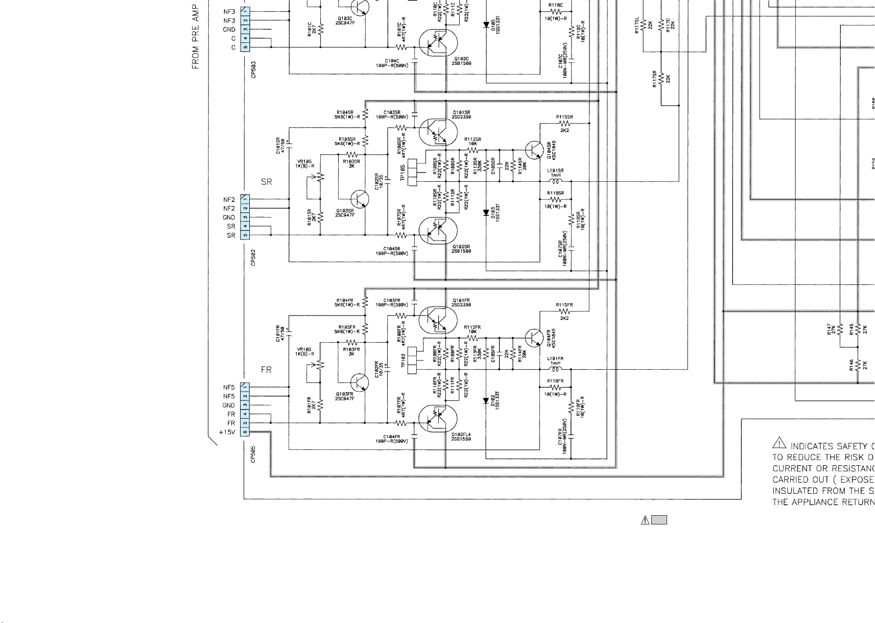
NOTICE:
ALL RESISTANCE VALUES IN OHM. k=1,000 OHM M=1,000,000 OHM
ALL CAPACITANCE VALUES IN MICRO FARAD. P=MICRO-MICRO FARAD
H VOLTAGE AND CURRENT ARE MEASUERD AT NO SIGNAL INPUT
EAC
CONDITION.
CIRCUIT AND PA
ICE.
NOT
RTS ARE SUBJECT TO CHANGE WITHOUT PRIOR
WARNING:
Parts marked with this symbol have critical characteristics.
Use ONLY replacement parts recommended by the manufacture.
CAUTION:
Before returning the unit to the customer, make sure you make either (1) a
leakage current check or (2) a line to chassis resistance check. If the leakage
current ex
of the powe
ceeds 0.5 milliamps, or if the resistance from chassis to either side
r card is less than 460kohms, the unit is defective.
WARNING:
DO NOT return the unit to the customer until the problem is located and
corrected.
Page 76

AVR-1603/683
A
B
C
D
Page 77

E
F
G
B LINE
SIGNAL LINE
SCHEMATIC DIAGRAMS (4/8)
MAIN UNIT
OUTLET UNIT
LTAGE SEL UNIT
VO
H
57
Page 78

SCHEMATIC DIAGRAMS (5/8)
1 2 3 4 5 6 7 8 9 10 11
AVR-1603/683
A
B
C
D
E
NOTICE:
ALL RESISTANCE VALUES IN OHM. k=1,000 OHM M=1,000,000 OHM
ALL CAPACITANCE VALUES IN MICRO FARAD. P=MICRO-MICRO FARAD
EACH VOLTAGE AND CURRENT ARE MEASUERD AT NO SIGNAL INPUT
CONDITION.
CIRCUIT AND PARTS ARE SUBJECT TO CHANGE WITHOUT PRIOR
NOTICE.
WARNING:
Parts marked with this symbol have critical characteristics.
Use ONLY replacement parts recommended by the manufacture.
CAUTION:
Before returning the unit to the customer, make sure you make either (1) a
leakage current check or (2) a line to chassis resistance check. If the leakage
current exceeds 0.5 milliamps, or if the resistance from chassis to either side
of the power card is less than 460kohms, the unit is defective.
WARNING:
DO NOT return the unit to the customer until the problem is located and
corrected.
F
G
B LINE
SIGNAL LINE
H
SCHEMATIC DIAGRAMS (5/8)
CPU UNIT
58
Page 79

SCHEMATIC DIAGRAMS (5/8)
1 2 3 4 5 6 7 8 9 10 11
AVR-1603/683
A
B
A
A
C
C
C
D
B
B
E
F
D
D
G
NOTICE:
ALL RESISTANCE VALUES IN OHM. k=1,000 OHM M=1,000,000 OHM
ALL CAPACITANCE VALUES IN MICRO FARAD. P=MICRO-MICRO FARAD
H VOLTAGE AND CURRENT ARE MEASUERD AT NO SIGNAL INPUT
EAC
CONDITION.
CIRCUIT AND PA
ICE.
NOT
RTS ARE SUBJECT TO CHANGE WITHOUT PRIOR
WARNING:
Parts marked with this symbol have critical characteristics.
Use ONLY replacement parts recommended by the manufacture.
CAUTION:
Before returning the unit to the customer, make sure you make either (1) a
leakage current check or (2) a line to chassis resistance check. If the leakage
current ex
of the powe
WARNING:
DO NOT return the unit to the customer until the problem is located and
corrected.
ceeds 0.5 milliamps, or if the resistance from chassis to either side
r card is less than 460kohms, the unit is defective.
B LINE
SIGNAL LINE
H
SCHEMATIC DIAGRAMS (5/8)
CPU UNIT
58
Page 80

SCHEMATIC DIAGRAMS (5/8)
1 2 3 4 5 6 7 8 9 10 11
Page 81

NOTICE:
ALL RESISTANCE VALUES IN OHM. k=1,000 OHM M=1,000,000 OHM
ALL CAPACITANCE VALUES IN MICRO FARAD. P=MICRO-MICRO FARAD
EAC
CONDITION.
CIRCUIT AND PA
NOT
Page 82

AVR-1603/683
A
B
C
D
Page 83

E
F
G
NOTICE:
ALL RESISTANCE VALUES IN OHM. k=1,000 OHM M=1,000,000 OHM
ALL CAPACITANCE VALUES IN MICRO FARAD. P=MICRO-MICRO FARAD
H VOLTAGE AND CURRENT ARE MEASUERD AT NO SIGNAL INPUT
EAC
CONDITION.
CIRCUIT AND PA
ICE.
NOT
RTS ARE SUBJECT TO CHANGE WITHOUT PRIOR
WARNING:
Parts marked with this symbol have critical characteristics.
Use ONLY replacement parts recommended by the manufacture.
CAUTION:
Before returning the unit to the customer, make sure you make either (1) a
leakage current check or (2) a line to chassis resistance check. If the leakage
current ex
of the powe
ceeds 0.5 milliamps, or if the resistance from chassis to either side
r card is less than 460kohms, the unit is defective.
WARNING:
DO NOT return the unit to the customer until the problem is located and
corrected.
B LINE
SIGNAL LINE
H
SCHEMATIC DIAGRAMS (5/8)
CPU UNIT
58
Page 84

SCHEMATIC DIAGRAMS (6/8)
1 2 3 4 5 6 7 8 9 10 11
AVR-1603/683
A
B
C
D
E
NOTICE:
ALL RESISTANCE VALUES IN OHM. k=1,000 OHM M=1,000,000 OHM
ALL CAPACITANCE VALUES IN MICRO FARAD. P=MICRO-MICRO FARAD
EACH VOLTAGE AND CURRENT ARE MEASUERD AT NO SIGNAL INPUT
CONDITION.
CIRCUIT AND PARTS ARE SUBJECT TO CHANGE WITHOUT PRIOR
NOTICE.
WARNING:
Parts marked with this symbol have critical characteristics.
Use ONLY replacement parts recommended by the manufacture.
CAUTION:
Before returning the unit to the customer, make sure you make either (1) a
leakage current check or (2) a line to chassis resistance check. If the leakage
current exceeds 0.5 milliamps, or if the resistance from chassis to either side
of the power card is less than 460kohms, the unit is defective.
WARNING:
DO NOT return the unit to the customer until the problem is located and
corrected.
SCHEMATIC DIAGRAMS (6/8)
VIDEO UNIT
VIDEO CNT UNIT
S-VIDEO UNIT
S-VIDEO CNT UNIT
C-VIDEO UNIT
F
G
B LINE
SIGNAL LINE
H
59
Page 85

SCHEMATIC DIAGRAMS (6/8)
1 2 3 4 5 6 7 8 9 10 11
AVR-1603/683
A
B
A
A
C
C
C
D
B
B
NOTICE:
ALL RESISTANCE VALUES IN OHM. k=1,000 OHM M=1,000,000 OHM
ALL CAPACITANCE VALUES IN MICRO FARAD. P=MICRO-MICRO FARAD
H VOLTAGE AND CURRENT ARE MEASUERD AT NO SIGNAL INPUT
EAC
CONDITION.
CIRCUIT AND PA
ICE.
NOT
WARNING:
Parts marked with this symbol have critical characteristics.
Use ONLY replacement parts recommended by the manufacture.
CAUTION:
Before returning the unit to the customer, make sure you make either (1) a
leakage current check or (2) a line to chassis resistance check. If the leakage
current ex
of the powe
WARNING:
DO NOT return the unit to the customer until the problem is located and
corrected.
RTS ARE SUBJECT TO CHANGE WITHOUT PRIOR
ceeds 0.5 milliamps, or if the resistance from chassis to either side
r card is less than 460kohms, the unit is defective.
D
D
SCHEMATIC DIAGRAMS (6/8)
VIDEO UNIT
VIDEO CNT UNIT
S-VIDEO UNIT
S-VIDEO CNT UNIT
C-VIDEO UNIT
E
F
G
B LINE
SIGNAL LINE
H
59
Page 86

SCHEMATIC DIAGRAMS (6/8)
1 2 3 4 5 6 7 8 9 10 11
Page 87

Page 88

AVR-1603/683
A
B
C
D
Page 89

E
F
NOTICE:
ALL RESISTANCE VALUES IN OHM. k=1,000 OHM M=1,000,000 OHM
ALL CAPACITANCE VALUES IN MICRO FARAD. P=MICRO-MICRO FARAD
H VOLTAGE AND CURRENT ARE MEASUERD AT NO SIGNAL INPUT
EAC
CONDITION.
CIRCUIT AND PA
ICE.
NOT
RTS ARE SUBJECT TO CHANGE WITHOUT PRIOR
WARNING:
Parts marked with this symbol have critical characteristics.
Use ONLY replacement parts recommended by the manufacture.
CAUTION:
Before returning the unit to the customer, make sure you make either (1) a
leakage current check or (2) a line to chassis resistance check. If the leakage
current ex
of the powe
ceeds 0.5 milliamps, or if the resistance from chassis to either side
r card is less than 460kohms, the unit is defective.
WARNING:
DO NOT return the unit to the customer until the problem is located and
corrected.
SCHEMATIC DIAGRAMS (6/8)
VIDEO UNIT
VIDEO CNT UNIT
S-VIDEO UNIT
S-VIDEO CNT UNIT
C-VIDEO UNIT
G
B LINE
SIGNAL LINE
H
59
Page 90

SCHEMATIC DIAGRAMS (7/8)
1 2 3 4 5 6 7 8 9 10 11
AVR-1603/683
A
B
C
D
E
NOTICE:
ALL RESISTANCE VALUES IN OHM. k=1,000 OHM M=1,000,000 OHM
ALL CAPACITANCE VALUES IN MICRO FARAD. P=MICRO-MICRO FARAD
EACH VOLTAGE AND CURRENT ARE MEASUERD AT NO SIGNAL INPUT
CONDITION.
CIRCUIT AND PARTS ARE SUBJECT TO CHANGE WITHOUT PRIOR
NOTICE.
WARNING:
Parts marked with this symbol have critical characteristics.
Use ONLY replacement parts recommended by the manufacture.
CAUTION:
Before returning the unit to the customer, make sure you make either (1) a
leakage current check or (2) a line to chassis resistance check. If the leakage
current exceeds 0.5 milliamps, or if the resistance from chassis to either side
of the power card is less than 460kohms, the unit is defective.
WARNING:
DO NOT return the unit to the customer until the problem is located and
corrected.
SCHEMATIC DIAGRAMS (7/8)
FRONT UNIT
OPTICAL-IN UNIT
POWER-SW UNIT
ENCODER UNIT
HEADPHONE UNIT
F
G
B LINE
SIGNAL LINE
H
60
Page 91

SCHEMATIC DIAGRAMS (7/8)
1 2 3 4 5 6 7 8 9 10 11
AVR-1603/683
A
B
A
A
C
C
C
D
B
B
E
F
D
D
G
NOTICE:
ALL RESISTANCE VALUES IN OHM. k=1,000 OHM M=1,000,000 OHM
ALL CAPACITANCE VALUES IN MICRO FARAD. P=MICRO-MICRO FARAD
H VOLTAGE AND CURRENT ARE MEASUERD AT NO SIGNAL INPUT
EAC
CONDITION.
CIRCUIT AND PA
ICE.
NOT
RTS ARE SUBJECT TO CHANGE WITHOUT PRIOR
WARNING:
Parts marked with this symbol have critical characteristics.
Use ONLY replacement parts recommended by the manufacture.
CAUTION:
Before returning the unit to the customer, make sure you make either (1) a
leakage current check or (2) a line to chassis resistance check. If the leakage
current ex
of the powe
ceeds 0.5 milliamps, or if the resistance from chassis to either side
r card is less than 460kohms, the unit is defective.
WARNING:
DO NOT return the unit to the customer until the problem is located and
corrected.
SCHEMATIC DIAGRAMS (7/8)
FRONT UNIT
OPTICAL-IN UNIT
ER-SW UNIT
POW
ENCODER UNIT
HEADPHONE UNIT
B LINE
SIGNAL LINE
H
60
Page 92

SCHEMATIC DIAGRAMS (7/8)
1 2 3 4 5 6 7 8 9 10 11
Page 93

NOTICE:
ALL RESISTANCE VALUES IN OHM. k=1,000 OHM M=1,000,000 OHM
ALL CAPACITANCE VALUES IN MICRO FARAD. P=MICRO-MICRO FARAD
H VOLTAGE AND CURRENT ARE MEASUERD AT NO SIGNAL INPUT
EAC
CONDITION.
CIRCUIT AND PA
ICE.
NOT
RTS ARE SUBJECT TO CHANGE WITHOUT PRIOR
WARNING:
Parts marked with this symbol have critical characteristics.
Use ONLY replacement parts recommended by the manufacture.
CAUTION:
Before returning the unit to the customer, make sure you make either (1) a
leakage current check or (2) a line to chassis resistance check. If the leakage
current ex
of the powe
ceeds 0.5 milliamps, or if the resistance from chassis to either side
r card is less than 460kohms, the unit is defective.
WARNING:
DO NOT return the unit to the customer until the problem is located and
corrected.
Page 94

AVR-1603/683
A
B
C
D
Page 95

E
F
G
SCHEMATIC DIAGRAMS (7/8)
FRONT UNIT
OPTICAL-IN UNIT
ER-SW UNIT
POW
ENCODER UNIT
HEADPHONE UNIT
B LINE
SIGNAL LINE
H
60
Page 96

SCHEMATIC DIAGRAMS (8/8)
1 2 3 4 5 6 7 8 9 10 11
AVR-1603/683
A
B
C
D
E
NOTICE:
ALL RESISTANCE VALUES IN OHM. k=1,000 OHM M=1,000,000 OHM
ALL CAPACITANCE VALUES IN MICRO FARAD. P=MICRO-MICRO FARAD
EACH VOLTAGE AND CURRENT ARE MEASUERD AT NO SIGNAL INPUT
CONDITION.
CIRCUIT AND PARTS ARE SUBJECT TO CHANGE WITHOUT PRIOR
NOTICE.
WARNING:
Parts marked with this symbol have critical characteristics.
Use ONLY replacement parts recommended by the manufacture.
CAUTION:
Before returning the unit to the customer, make sure you make either (1) a
leakage current check or (2) a line to chassis resistance check. If the leakage
current exceeds 0.5 milliamps, or if the resistance from chassis to either side
of the power card is less than 460kohms, the unit is defective.
WARNING:
DO NOT return the unit to the customer until the problem is located and
corrected.
F
G
B LINE
SIGNAL LINE
H
SCHEMATIC DIAGRAMS (8/8)
TUNER UNIT
61
Page 97

SCHEMATIC DIAGRAMS (8/8)
1 2 3 4 5 6 7 8 9 10 11
AVR-1603/683
A
B
A
A
C
C
C
D
B
B
E
F
D
D
G
NOTICE:
ALL RESISTANCE VALUES IN OHM. k=1,000 OHM M=1,000,000 OHM
ALL CAPACITANCE VALUES IN MICRO FARAD. P=MICRO-MICRO FARAD
H VOLTAGE AND CURRENT ARE MEASUERD AT NO SIGNAL INPUT
EAC
CONDITION.
CIRCUIT AND PA
ICE.
NOT
RTS ARE SUBJECT TO CHANGE WITHOUT PRIOR
WARNING:
Parts marked with this symbol have critical characteristics.
Use ONLY replacement parts recommended by the manufacture.
CAUTION:
Before returning the unit to the customer, make sure you make either (1) a
leakage current check or (2) a line to chassis resistance check. If the leakage
current ex
of the powe
ceeds 0.5 milliamps, or if the resistance from chassis to either side
r card is less than 460kohms, the unit is defective.
WARNING:
DO NOT return the unit to the customer until the problem is located and
corrected.
B LINE
SIGNAL LINE
H
SCHEMATIC DIAGRAMS (8/8)
TUNER UNIT
61
Page 98

SCHEMATIC DIAGRAMS (8/8)
1 2 3 4 5 6 7 8 9 10 11
Page 99

NOTICE:
ALL RESISTANCE VALUES IN OHM. k=1,000 OHM M=1,000,000 OHM
ALL CAPACITANCE VALUES IN MICRO FARAD. P=MICRO-MICRO FARAD
H VOLTAGE AND CURRENT ARE MEASUERD AT NO SIGNAL INPUT
EAC
CONDITION.
CIRCUIT AND PA
ICE.
NOT
RTS ARE SUBJECT TO CHANGE WITHOUT PRIOR
WARNING:
Parts marked with this symbol have critical characteristics.
Use ONLY replacement parts recommended by the manufacture.
CAUTION:
Before returning the unit to the customer, make sure you make either (1) a
leakage current check or (2) a line to chassis resistance check. If the leakage
current ex
of the powe
ceeds 0.5 milliamps, or if the resistance from chassis to either side
r card is less than 460kohms, the unit is defective.
WARNING:
DO NOT return the unit to the customer until the problem is located and
corrected.
Page 100

AVR-1603/683
A
B
C
D
 Loading...