

Page 1
For U.S.A., Canada, Europe,
Asia, China, Hong Kong &
Taiwan R.O.C. model
SERVICE MANUAL
Hi-Fi Component
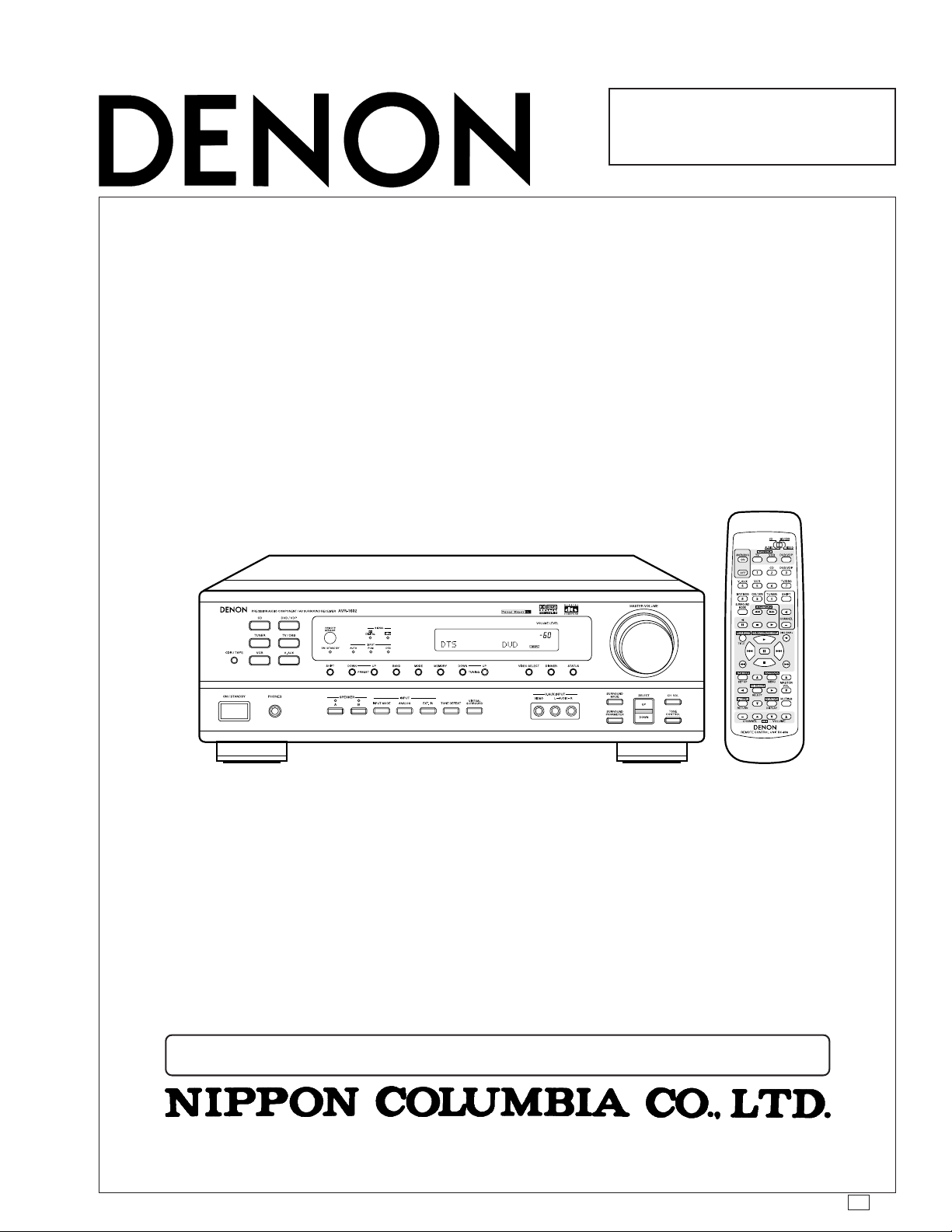
MODEL
AVR-1602/682
AV SURROUND RECEIVER
Some illustrations using in this service manual are slightly different from the actual set.
14-14, AKASAKA 4-CHOME, MINATO-KU, TOKYO 107-8011 JAPAN
Telephone: 03 (3584) 8111
X0116 1174 NC 0111
Page 2

AVR-1602/682
SAFETY PRECAUTIONS
The following check should be performed for the continued protection of the customer and service technician.
LEAKAGE CURRENT CHECK
Before returning the unit to the customer, make sure you make either (1) a leakage current check or (2) a line to chassis
resistance check. If the leakage current exceeds 0.5 milliamps, or if the resistance from chassis to either side of the
power cord is less than 460 kohms, the unit is defective.
SPECIFICATIONS
Audio Section
Power Amplifier
Rated output: Front: 70W+70W (8Ω/ohms, 20Hz~20kHz with 0.08% T.H.D )
Center: 70W (8Ω/ohms, 20Hz~20kHz with 0.08% T.H.D )
Surround: 70W+70W (8Ω/ohms, 20Hz~20kHz with 0.08% T.H.D )
Output terminals: Front: A or B 6 to 16W/ohms
Center/Surround: 6 to 16W/ohms
100W+100W (6Ω/ohms, 1kHz with 0.7% T.H.D )
110W+110W (6Ω/ohms, EIAJ ) (Asia Model)
100W (6Ω/ohms, 1kHz with 0.7% T.H.D )
110W (6Ω/ohms, EIAJ ) (Asia Model)
100W+100W (6Ω/ohms, 1kHz with 0.7% T.H.D )
110W+110W (6Ω/ohms, EIAJ ) (Asia Model)
A+B 12 to 16W/ohms
Analog
LINE input - PRE OUT
Input sensitivity/input impedance:
Frequency response: 10Hz~100kHz: +1, −3dB (TONE DEFEAT ON)
S/N ratio: 98dB (IHF-A weighted) (TONE DEFEAT ON)
200mV/47kΩ/kohms
(U.S.A., Canada & Europe Models)
(U.S.A., Canada & Europe Models)
(U.S.A., Canada & Europe Models)
Video Section
Standard video jacks
Input/output level and impedance:
Frequency response: 5Hz~10MHz +1, −3dB
1Vp-p,75Ω/ohms
S-video jacks (U.S.A., Canada & Asia Models)
Input/output level and impedance:
Frequency response: 5Hz~10MHz: +1, −3dB
Tuner section
Receiving range: [FM] (note: µV at 75Ω/ohms, 0dBf =1×10
U.S.A., Canada Models:
Europe & Asia (for China) Models:
Asia (for Multiple voltage) Models:
Usable sensitivity: 1.0µV (11.2dBf) 18µV
50 dB quieting sensitivity: MONO 1.6µV (15.3dBf)
S/N ratio: MONO 80dB (IHF-A weighted)
Total harmonic distortion: MONO 0.15% (1kHz)
General
Power supply:
U.S.A., Canada Models AC120V,60Hz
Europe Model AC230V,50Hz
Asia(for Multiple voltage)Model AC115/230V,50/60Hz
Asia(for China)Model AC220V,50Hz
Power consumption: 3.7A (USA & Canada model), 200W (Europe & Asia model)
Maximum external dimensions: 434 (W) × 147 (H) × 417 (D) mm (17-3/32″ × 5-25/32″ × 16-7/16″)
Mass: 9.8kg (20 lbs 9.7 oz)
Y(brightness)signal 1Vp-p, 75Ω/ohms
C(color)signal 0.286Vp-p, 75Ω/ohms
-15
87.50MHz~107.90MHz 520kHz~1710kHz
87.50MHz~108.00MHz 522kHz~1611kHz
87.50MHz~107.90MHz (0.2MHz steps) 520kHz~1710kHz (10kHz steps)
87.50MHz~108.00MHz (0.05MHz steps) 522kHz~1611kHz (9kHz steps)
STEREO 23µV (38.5dBf)
STEREO 75dB (IHF-A weighted)
STEREO 0.3% (1kHz)
W) [AM]
Remote control unit (RC-896)
Batteries: R6P/AA Type (two batteries)
External dimensions: 54 (W) × 172.5 (H) × 29 (D) mm (2-1/8″ × 6-51/64″ × 1-9/64″)
Mass: 120g (Approx. 4.2 oz) (including batteries)
* For purposes of improvement, specifications and design are subject to change without notice.
2
Page 3
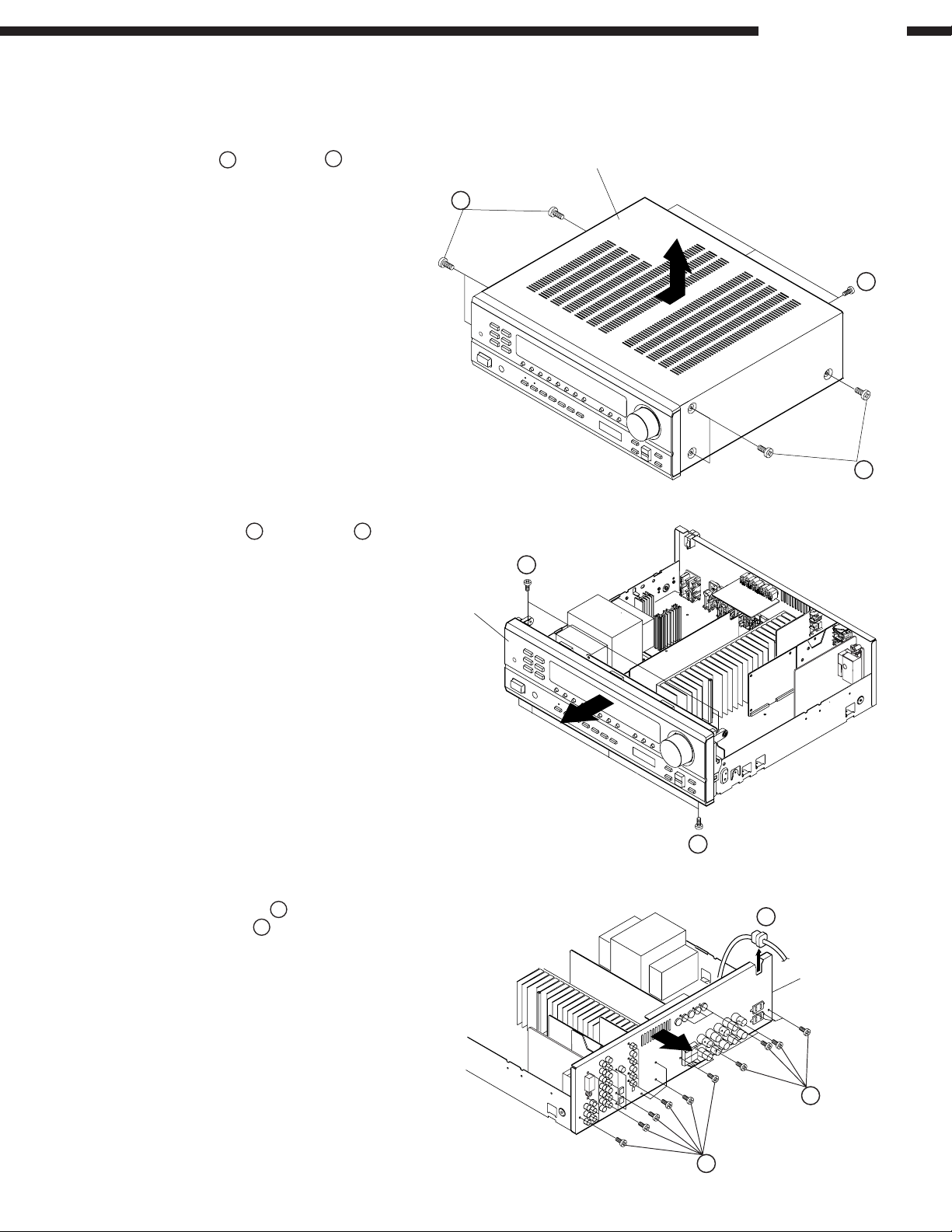
DISASSEMBLY
(Follow the procedure below in reverse order when reassembling)
Top Cover
Remove 6 screws
in the arrow direction.
and 3 screws 2, detach the Top Cover
1
1
AVR-1602/682
Top Cover
2
1
Front Panel
1. Remove 4 screws
2. Detach the Front Panel in the arrow direction.
and 2 screws 4.
3
Rear Panel
5
1. Remove cord bushing
2. Remove 31 screws
3. Detach the Rear Panel in the arrow direction.
from the Rear Panel.
.
6
4
Front Panel
3
5
Rear Panel
6
6
3
Page 4
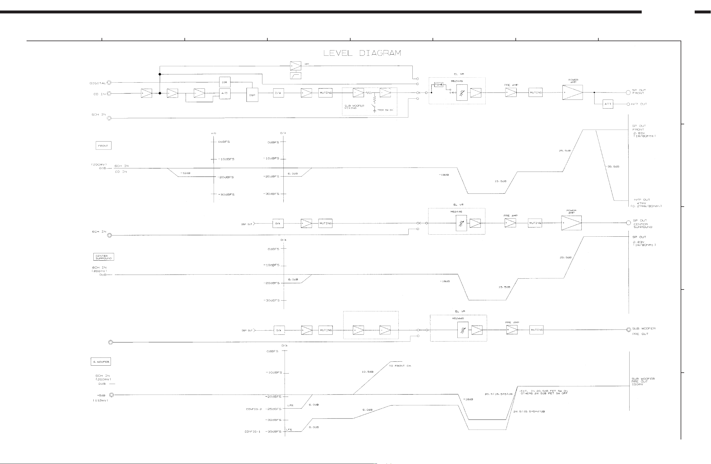
LEVEL DIAGRAM
1
AVR-1602/682
2
3
4
5
76
8
A
B
C
D
E
4
Page 5
8
76
5
4
3
2
1
A
B
C
D
E
AVR-1602/682
5
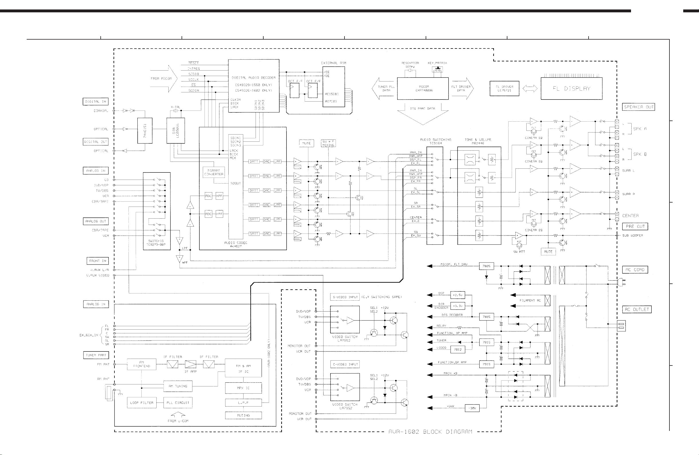
BLOCK DIAGRAM
Page 6
ADJUSTMENT
Tuner Section
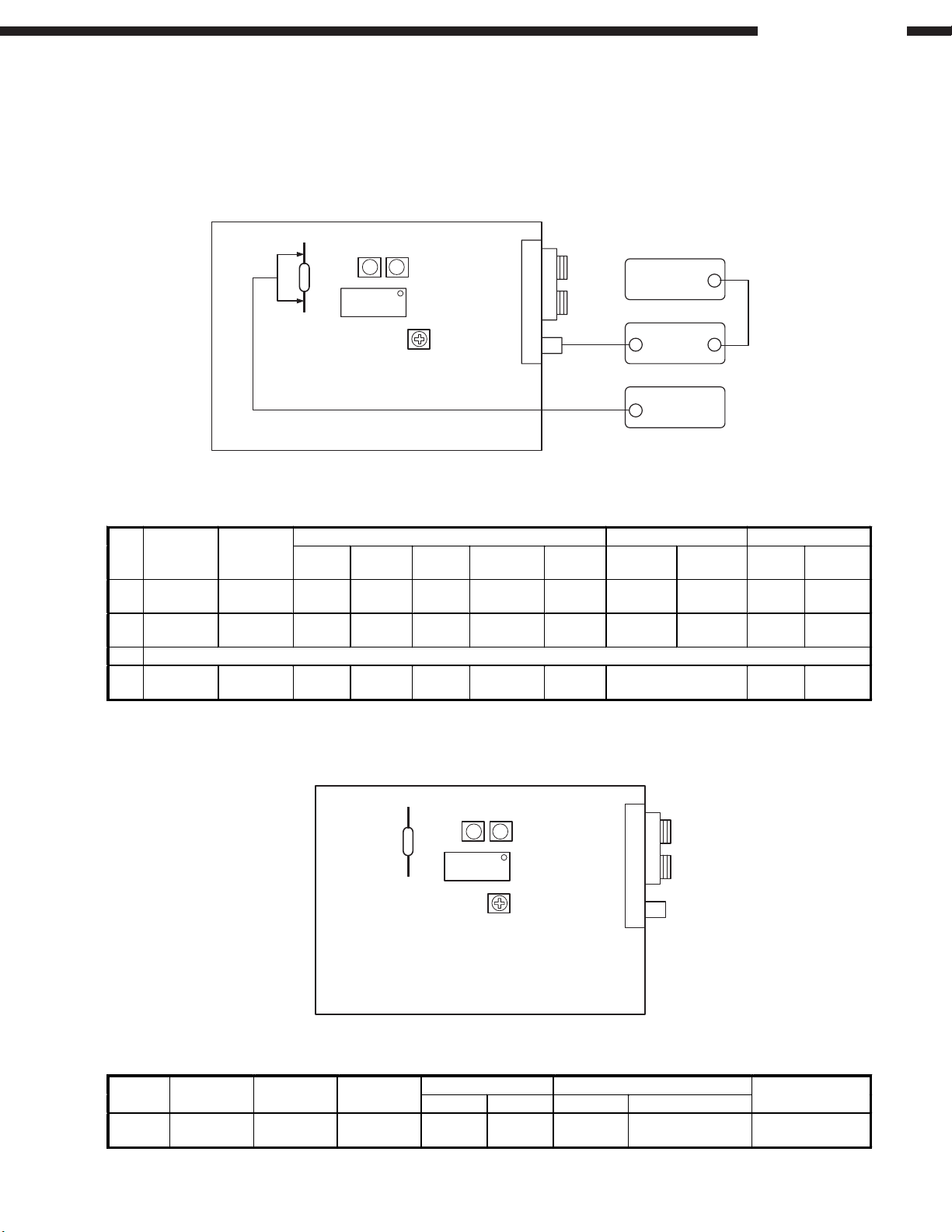
CONNECTION DIAGRAM OF MEASURING INSTRUMENTS
FM
T402 T403
R471
IC402
AVR-1602/682
STEREO
MODULATOR
VR402
TUNER B'D
FM ALIGNMENT
Alignment
Step
AM
Item
Center
1
Adjustment
2 Distortion
3 Repeat Steps 1 and 2
4 Signal Level
Tuning
Frequency
Setting
98.1MHz
(98.0MHz)
98.1MHz
(98.0MHz)
98.1MHz
(98.0MHz)
Type Frequency
FM SSG 98.1MHz 60dBP
FM SSG 98.1MHz 60dBP
FM SSG 98.1MHz 20dBP OFF
Input Output Adjustment
Input
Level
Modulation Coupling Type Connect to Points Adjust to
Mono
1kHz 100%
Mono
1kHz 100%
75ohm
Antenna
Terminal
Antenna
Terminal
Antenna
Terminal
FM SSG
Digital
Voltmeter
Digital
Volt me te r
Distortion
Meter
Light “TUNED” on
Terminal (L)
FL Display
R471 T402 r 50mV
Output
T403
VR402
Minimum
Distortion
+14
20
−10
dB
AM ALIGNMENT
Step
1 Signal Level
Alignment
Item
Frequency Input
999 (1000)
kHz
AM SSG VR401
T402 T403
R471
IC402
VR401
TUNER B’D
Output Adjustment
Type Connect to Points Adjust to
Light “TUNED” on
FL Display
Remarks
SSG OUTPUT
74dBP (EMF)
6
Page 7
AVR-1602/682
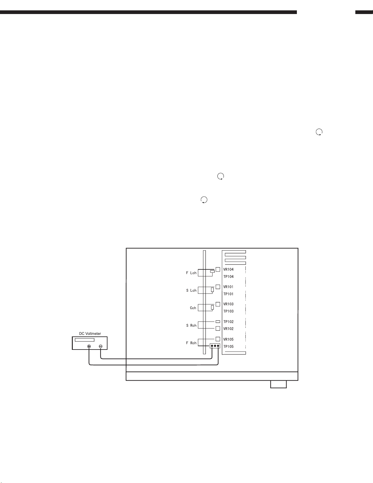
Audio Section
Idling Current
Required measurement equipment : DC Voltmeter
Preparation
(1) Avoid direct blow from an air conditioner or an electric fan, and adjust the unit at normal room tempereture
15 °C ~ 30 °C (59 °F ~ 86 °F).
(2) Presetting
● POWER (Power sourse switch) → OFF
● SPEAKER (Speaker terminal) → No load (Do not connect speaker, dummy resistor, etc.)
Adjustment
(1) Remove top cover and set VR101, VR102, VR103, VR104, VR105 on Amp. Unit at full counterclockwise ( )
position.
(2) Connect DC Voltmeter to test points (FRONT-Lch: TP104, FRONT-Rch: TP105, CENTER ch: TP103,
SURROUND-Lch: TP101, SURROUND-Rch: TP102).
(3) Connect power cord to AC Line, and turn power switch "ON".
(4) Presetting. MASTER VOLUME : "---" counterclockwise (
MODE : 5CH STEREO
FUNCTION : CD
(5) Within 2 minutes after the power on, turn VR101 clockwise (
DC.
(6) After 10 minutes from the preset above, turn VR101 to set the voltage to 2.5 mV ±0.5 mV DC.
(7) Adjust the Variable Resistors of other channels in the same way.
min.)
) to adjust the TEST POINT voltage to 1.5 mV ±0.5 mV
7
Page 8
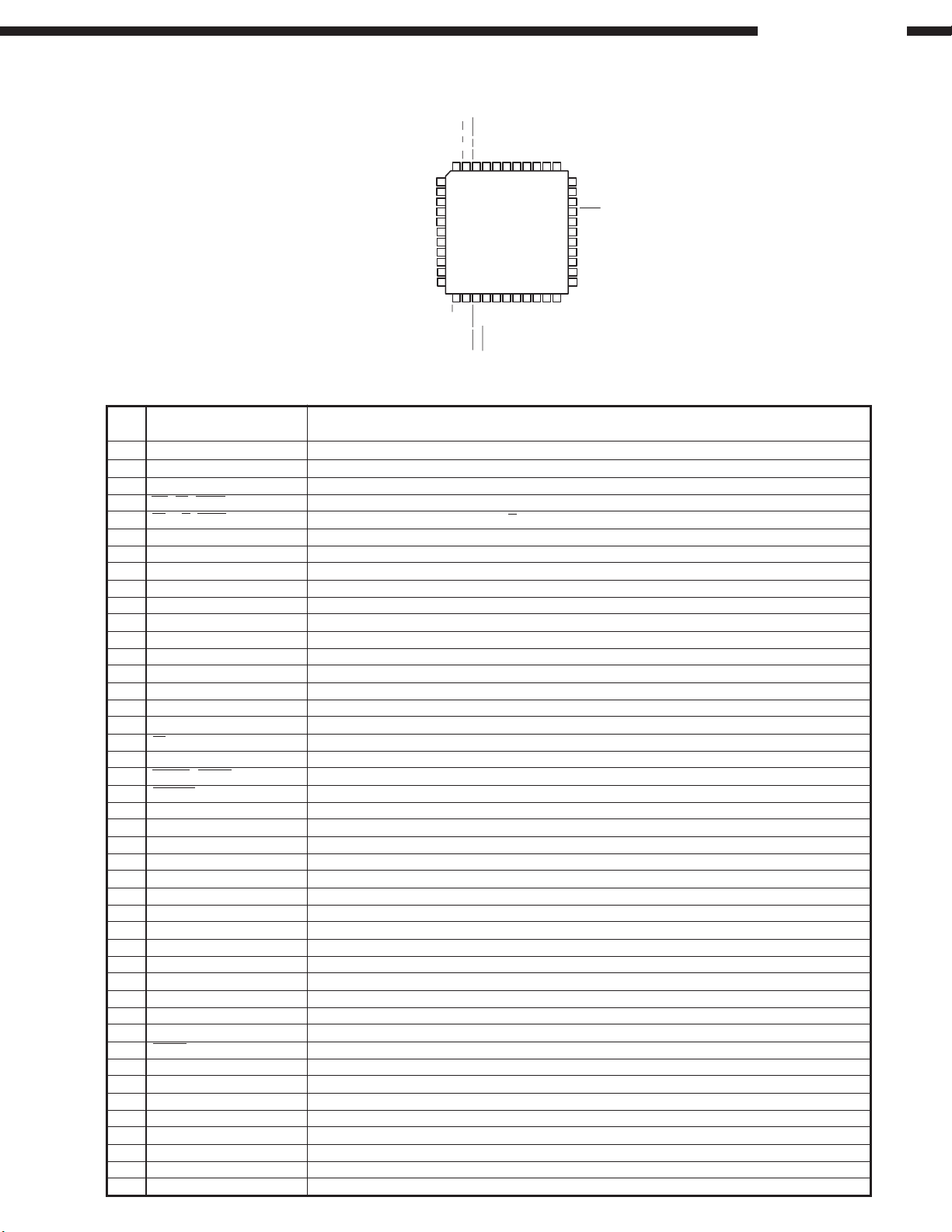
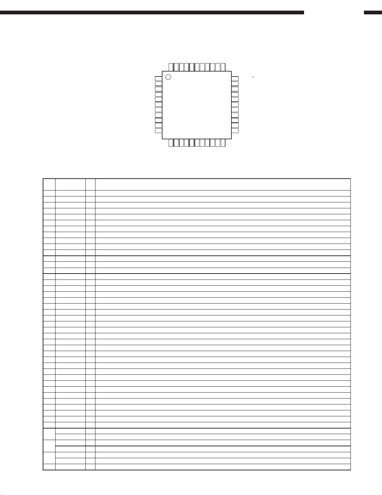
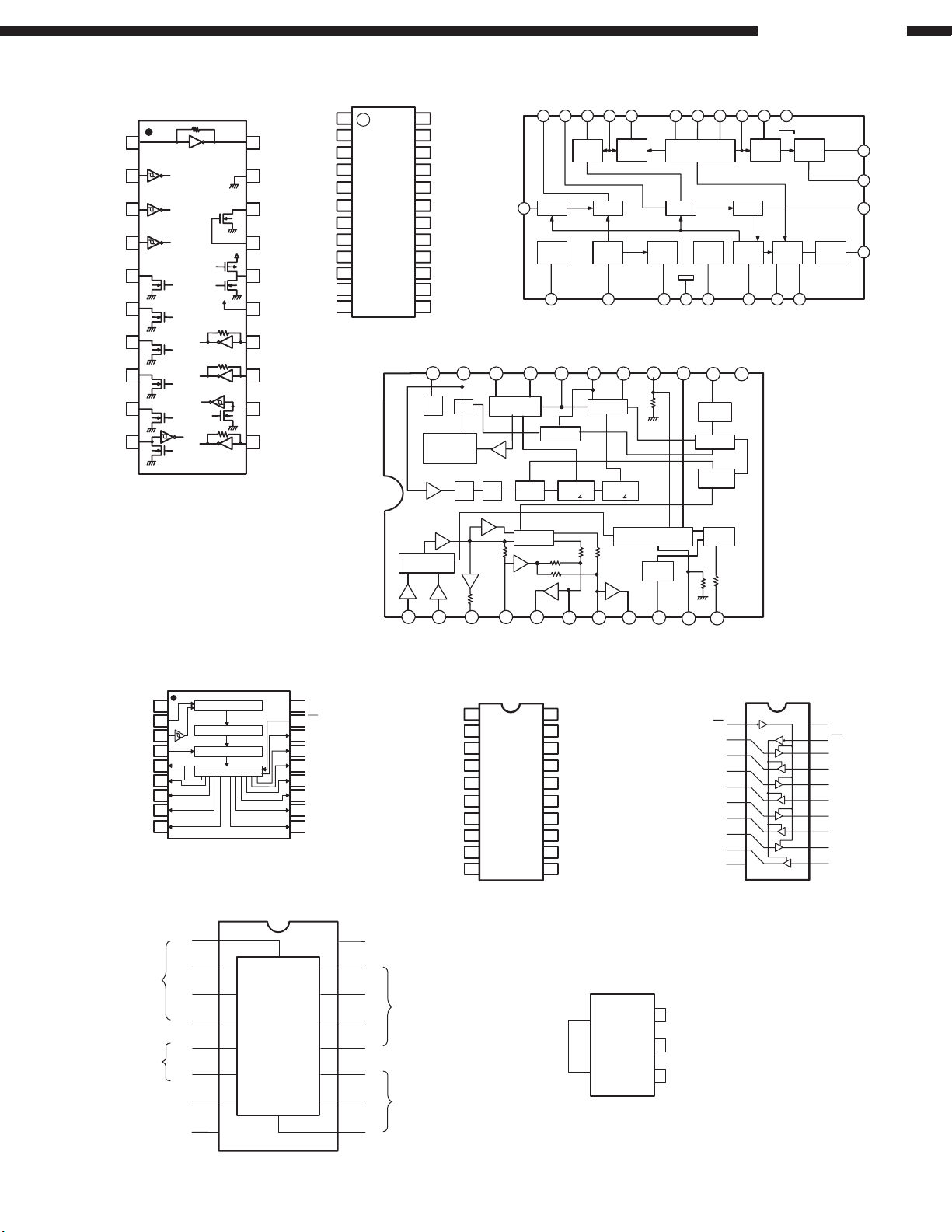
SEMICONDUCTORS
IC’s
CS49326-CL
(IC812)
A0,SCCLK
DATA7,EMAD7,GPIO7
DATA6,EMAD6,GPIO6
DATA5,EMAD5,GPIO5
DATA4,EMAD4,GPIO4
DATA3,EMAD3,GPIO3
DATA2,EMAD2,GPIO2
DATA1,EMAD1,GPIO1
DATA0,EMAD0,GPIO0
VD2
DGND2
AVR-1602/682
A1,SCDIN
RD,R/W,EMOE,GPIO11
WR,DS,EMWR,GPIO10
AUDATA3,XMT958
DGND1
VD1
MCLK
SCLK
LRCLK
AUDATA0
AUDATA1
44
56
21 22
ABOOT,INTREQ
1234
SDATAN1
EXTMEM,GPIO8
7
8
9
10
11
12
13
14
15
16
17
18 19 20
CS
404142
43
39
AUDATA2
38
DC
37
DD
RESET
36
AGND
35
34
VA
FILT1
33
FILT2
32
CLKSEL
31
CLKIN
30
CMPREQ,LRCLKN2
29
282726252423
VD3
DGND3
LRCLKN1
CMPCLK,SCLKN2
SCLKN1,STCCLK2
CS49326-CL Terminal Function
Pin
No.
Pin Name
SCDIO,SCDOUT,PSEL,GPIO9
CMPDAT,SDATAN2,RCV958
Function
1 VD1 Digital positive supply
2 DGND1 Digital supply ground
3 AUDATA3, XMT958 SPDIF transmitter output, Digital audio output 3
4 WR, DS, EMWR, GPIO10 Host write strobe or host data strobe or external memory write enable or general purpose input & output number 10
5 RD, R/W, EMOE, GPIO11
Host parallel output enable or host parallel R/W or external memory output enable or general purpose input & output number11
6 A1, SCDIN Host address bit one or SPI serial control data input
7 A0, SCCLK Host parallel address bit zero or serial control port clock
8 DATA7, EMAD7, GPIO7
9 DATA6, EMAD6, GPIO6
10 DATA5, EMAD5, GPIO5
11 DATA4, EMAD4, GPIO4
12 VD2 Digital positive supply
13 DGND2 Digital supply ground
14 DATA3, EMAD3, GPIO3
15 DATA2, EMAD2, GPIO2
16 DATA1, EMAD1, GPIO1
17 DATA0, EMAD0, GPIO0
18 CS Host parallel chip select, host serial SPI chip select
19 SCDIO, SCDOUT, PSEL, GPIO9 Serial control port data input and output, parallel port type select
20 INTREQ, ABOOT Control port interrupt request, automatic boot enable
21 EXTMEM, GPIO8 External memory chip select or general purpose input & output number 8
22 SDATAN1 PCM audio data input number one
23 VD3 Digital positive supply
24 DGND3 Digital supply ground
25 SCLKN1, STCCLK2 PCM audio input bit clock
26 LRCLKN1 PCM audio input sample rate clock
27 CMPDAT, SDATAN2, RCV958 PCM audio data input number two
28 CMPCLK, SCLKN2 PCM audio input bit clock
29 CMPREQ, LRCLKN2 PCM audio input sample rate clock
30 CLKIN Master clock input
31 CLKSEL DSP clock select
32 FILT2 Phase locked loop filter
33 FILT1 Phase locked loop filter
34 VA Analog positive supply
35 AGND Analog supply ground
36 RESET Master reset input
37 DD Reserved
38 DC Reserved
39 AUDATA2 Digital audio output 2
40 AUDATA1 Digital audio output 1
41 AUDATA0 Digital audio output 0
42 LRCLK Audio output sample rate clock
43 SCLK Audio output bit clock
44 MCLK Audio master clock
8
Page 9
AVR-1602/682
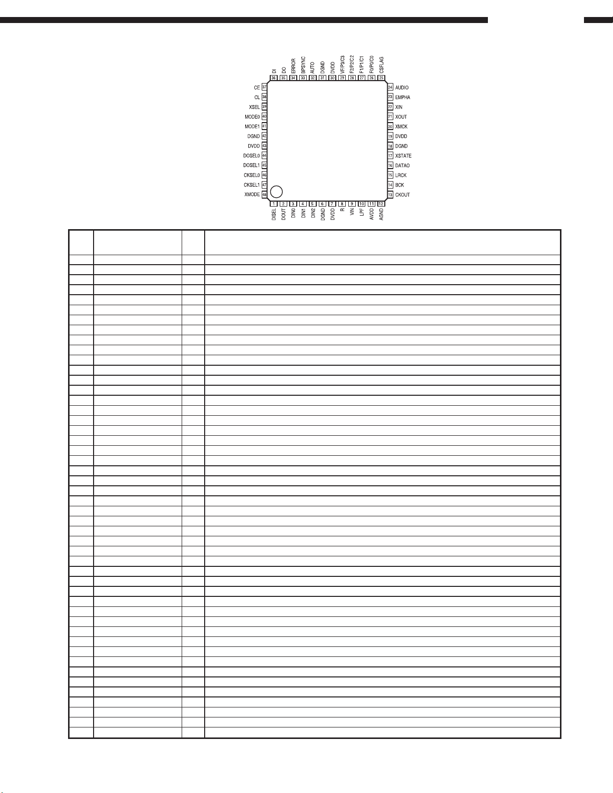
LC89055W (IC810)
LC89055W Terminal Function
Pin
No.
1 DISEL I Data input terminal (select input pin of DIN0, DIN1)
2 DOUT O Input bi-phase data through output terminal
3 DIN0 I Amp built-in coaxial/optical input correspond data input terminal
4 DIN1 I Amp built-in coaxial/optical input correspond data input terminal
5 DIN2 I Optical input correspond data input terminal
6 DGND Digital GND
7 DVDD Digital power supply
8 R I VCO gain control input terminal
9 VIN I VCO free-run frequency setting input terminal
10 LPF O PLL loop filter setting terminal
11 AVDD Analog power supply
12 AGND Analog GND
13 CKOUT O Clock output terminal (256fs, 384fs, 512fs, X’tal osc., VCO free-run osc.)
14 BCK O 64fs clock output terminal
15 LRCK O fs clock output terminal (L: Rch, H: Lch, I2S: Reverse)
16 DATAO O Data output terminal
17 XSTATE O Input data detecting result output terminal
18 DGND Digital GND
19 DVDD Digital power supply
20 XMCK O X’tal osc. clock output terminal (24.576MHz or 12.288MHz)
21 XOUT O X’tal osc. connection output terminal
22 XIN I X’tal osc. connection input terminal, external signal input possible (24.576MHz or 12.288MHz)
23 EMPHA O Emphasis information output terminal of channel status
24 AUDIO O Bit1 output terminal of channel status
25 CSFLAG O Top 40bit revise flag output terminal of channel status
26 F0/P0/C0 O Input fs cal. sig. out/data type out/input word inf. output terminal
27 F1/P1/C1 O Input fs cal. sig. out/data type out/input word inf. output terminal
28 F2/P2/C2 O Input fs cal. sig. out/data type out/input word inf. output terminal
29 VF/P3/C3 O Validity flag out/data type out/input word inf. output terminal
30 DVDD Digital power supply
31 DGND Digital GND
32 AUTO O Non PCM burst data transfer detect sig. output terminal
33 BPSYNC O Non PCM burst data preamble Pa, Pb, Pc, Pd sync sig. output terminal
34 ERROR O PLL lock error, data error flag output terminal
35 DO O CPU/IFD read data output terminal
36 DI I CPU I/F write data input terminal
37 CE I CPU I/F chip enable input terminal
38 CL I CPU I/F chip enable input terminal
39 XSEL I Frequency select input pin of XIN X’tal osc. (24.576MHz or 12.288MHz)
40 MODE0 I Mode setting input terminal
41 MODE1 I Mode setting input terminal
42 DGND Digital GND
43 DVDD Digital power supply
44 DOSEL0 I Data output format select input terminal
45 DOSEL1 I Data output format select input terminal
46 CKSEL0 I Output clock select input terminal
47 CKSEL1 I Output clock select input terminal
48 XMODE I Reset input terminal
For latch-up countermeasure, set digital (DVDD) and analog (AVDD) power on/off in the same timing.
Pin Name FunctionI/O
9
Page 10
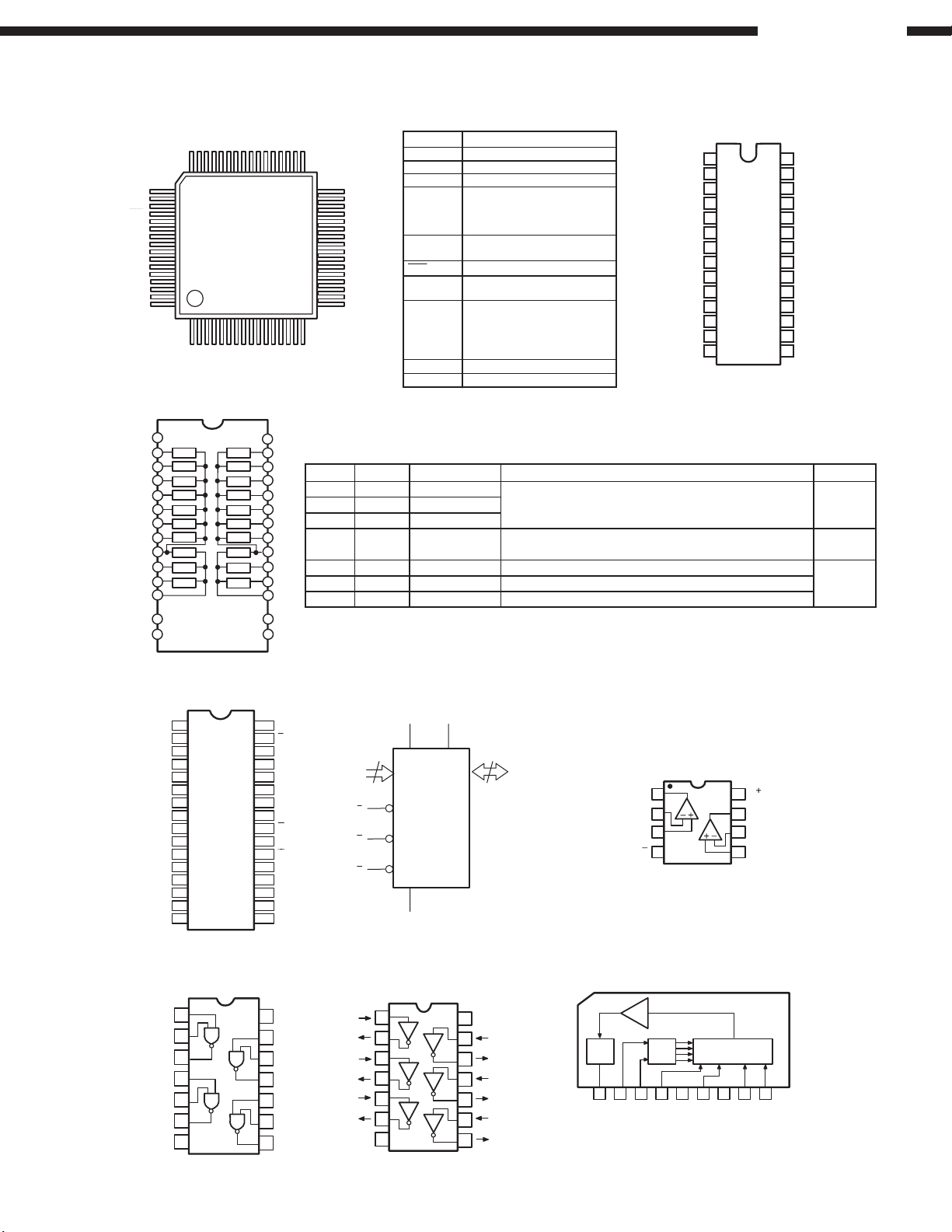
AK4527BVQ (IC813)
L0OP1
L0OP0/SDA/CDTI
444342
DIF1/SCL/CCLK
DIF0/CSN
P/S
MCLK
39
38
40
41
DZF1
37
AVSS
36
AVDD
35
VCOM
VREFH
34
AVR-1602/682
22
CAD1
CAD0
33
DZ F2/OVF
32
RIN+
31
RIN–
30
LIN+
29
LIN–
28
ROUT1
27
LOUT1
26
ROUT2
25
LOUT2
24
ROUT3
23
LOUT3
SDOS
I2C
SMUTE
BICK
LRCK
SDTI1
SDTI2
SDTI3
SDTO
DAUX
DFS
1
2
3
4
5
6
7
8
9
10
11
12
13 14
NC
AK4527BVQ
15
TVDD
DZ FE
Top View
16 17 18
PDN
DVSS
DVDD
192021
NC
TST
ADIF
AK4527BVQ Terminal Function
Pin
Pin Name I/O Function
No.
1 SDOS I SDTO source select pin, L: Internal ADC output, H: DAUX input
2 I2C I Serial control mode select pin, L: 3-core serial, H: I2C bus
3 SMUTE I Soft mute pin, H: Soft mute start, L: Release
4 BICK I Audio serial data clock pin
5 LRCK I Input channel clock pin
6 SDTI1 I DAC1 audio serial data input pin
7 SDTI2 I DAC2 audio serial data input pin
8 SDTI3 I DAC3 audio serial data input pin
9 SDTO O Audio serial data output pin
10 DAUX I Auxiliary audio serial data input pin
11 DFS I Double speed sampling mode pin, L: Normal, H: Double
12 NC No Connect, No internal bonding
13 DZFE I Zero input detect enable pin
14 TVDD Power pin for output buffer, 2.7V~5.5V
15 DVDD Digital power pin, 4.5V~5.5V
16 DVss Digital GND pin, 0V
17 PDN I Power down & reset pin, L: Powered-down and register initialized, Reset with PDN when switching P/S or CAD0-1
18 TST I Test pin, connected to DVSS
19 NC No Connect, No internal bonding
20 ADIF I Analog Input Format Select pin
21 CAD1 I Chip address-1 pin
22 CAD0 I Chip address-0 pin
23 LOUT3 O DAC3L channel analog out pin
24 ROUT3 O DAC3R channel analog out pin
25 LOUT2 O DAC2L channel analog out pin
26 ROUT2 O DAC2R channel analog out pin
27 LOUT1 O DAC1L channel analog out pin
28 ROUT1 O DAC1R channel analog out pin
29 LIN- I L-ch analog inverted input pin
30 LIN+ I L-ch analog non-inverted input pin
31 RIN- I R-ch analog inverted input pin
32 RIN+ I R-ch analog non-inverted input pin
33 DZF2/OVF O 0 input detect 2 pin/Analog input overflow detect pin
34 VCOM O Common V-out pin, AVDD/2, connect large capacitor to avoid noise
35 VREFH I Ref. V input pin, AVDD
36 AVDD Analog GND pin, 4.5V~5.5V
37 AVss Analog GND pin, 0V
38 DZF1 O 0 input detect pin, H: Input data of G1 is 8192 times “0” in a raw or RSTN bit “0”
39 MCLK I Master clock input pin
40 P/S I Parallel/Serial select pin, L: Serial control
DIF0 I Audio data I/F format 0 pin (parallel control)
41
CSN I Chip select pin (3-wire serial control), connect to DVDD when I
DIFI I Audio data I/F format 1 pin (parallel control)
42
SCL/CCLK I Control data clock pin (serial control), I
LOOP0 I Loop back mode 0 pin (parallel control), effects digital loop back ADC to all DAC
43
SDA/CDTI I/O Control data input pin (serial control), I2C=”L”: CCTI (3-wire serial), I2C =”H” SDA (I2C bus)
2
C=”L”: CCLK (3-wire serial), I2C=”H”: SCL (I2C bus)
44 LOOP1 I Loop back mode 1 pin, from SDT1 to all DAC
2
C bus control
10
Page 11
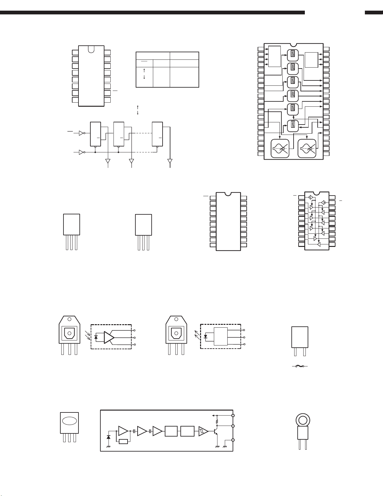
AVR-1602/682
1
2
3
4
5
6
7
8
18
17
16
15
14
13
12
11
Q3
VDD
OE
Q7
Q8
Q11
Q10
Q9
Q6
VSS
DATA
CLOCK
LCK
Q0
Q1
Q2
9
10
Q4
Q5
CONTROL CIRCUIT
12-bit SHIFT RESISTER
12-bit STRAGE RESISTER
OUTPUT BUFFER (OPEN DRAIN)
BU2090F (IC302)
1
MM74LCX244 (IC818,819)
RC1117S25T (IC820)
RC1117S33ST (IC811)
2
3
2
ADJ/GND
OUT
IN
MM74HC151 (IC832)
V
OUT
FRONT VIEW
LA1266 (IC402)
10
4
1
3
8
19
15
17
18
14
21
22
GND
Vcc
5
11
IF
BUFFER
IF
BUFFER
2
F M - IF
6
Q.D.
7
REG
23
OSC
OSC
BUFFER
24
NARROW
S-M ETER
S-M ETER
16
LED
DRIVER
RF MIX
12
20
AM -IF DET
AGC
POST
AM P
9
13
AM -IF FM-IF FM -IN
AM-IN
20
19
18
17
16
15
14
13
12
9
8
7
5
6
1
21
LA3401 (IC403)
22
VOL
REG
OSC
SYMM ETRICAL
REOCTANCE
CIRCUIT
PHASE
COM PARATO R
VCO STOP
PILOT DET
FF
FF
FF
38kHz
FF
38kHz 90°FF19kHz 90°
MUTING
FM AM CHANGE
Ro
Rc
Rc
Rb
2
3
4
DECODER
M UTIN G CO NTR O L
FM AM CHANGE O VER
Vcc ON
MUTING
MUTING
OUTPUT
STEREO
SW ITCH
TRIG G ER
LAM P
DRIVER
Rb
10
11
LC72131 (IC401)
1
20
2
19
3
18
417
5
16
6
15
7
14
8
13
9 12
10 11
XIN
CE
DI
CL
DO
BO1
BO2
BO3
BO4
IO 1
AOU T
AIN
PD
VDD
FM IN
AM IN
IO 2
IF IN
Vss
XOU T
TDA7330BD (IC202)
TOP VIEW
POR
MUXIN
TM
V
REF
FSEL
COMP
T2
FILOUT
V
CC
GND
ARI
T1
QUAL
T3
RDDA
T4
RDCL
OSCOUT
T57
OSCIN
1
2
3
4
5
6
7
8
9
10
20
19
18
17
16
15
14
13
12
11
124
12 13
1
2
3
4
5
6
7
8
20
19
18
16
15
14
13
I3
VCC
OE2
O2
I5
O0
I4
O1
I6
OE
I0
O4
I1
O5
I2
O6
912
O7
O3
10
11
GND
I7
TOP VIEW
D4
D5
D6
D7
A
B
D2
D1
D0
Y
W
S
D3
C
4
5
6
7
A
B
C
Vcc
15
14
13
12
11
10
9
16
2
3
4
5
6
7
8
1
2
1
0
Y
W
ST ROBE
GND
3
DATA
INPUTS
OUTPUTS
DATA
INPUTS
DATA
SELECT
TOP VIEW
17
11
Page 12
AVR-1602/682
LC75721E (IC301)
G7 G8G9
G10
G11
AA8/G12
AA7/G13
48 33
49
DI
CL
CE
RES
V
DD
OSCI
OSCO
Vss
TEST
V
FL
G1
G2
G3
G4
G5
G6
64
AM 1
AM 2
AM 3
AM 4
AM 5
AM 6
AM 7
TC9273N-007(IC701)
1
Vss
2
S1
S2
3
4
S3
5
S4
6
S5
7
S6
8
S7
9
S8
10
S9
11
S10
12
13
GND
14
CK
V
S1
S2
S3
S4
S5
S6
S7
S8
S9
S10
STB
DAT A
AA6/G14
AA5/G15
AA4/G16
AM 8
AM 9
DD
KIC9164AN (IC221)
LC75721E Terminal Function
AA3
AA2
AA1
AM35
AM34
AM33
32
AM 17
AM 18
AM 19
AM 20
AM 21
AM 22
AM 23
AM 24
AM 25
AM 26
AM 27
AM 28
AM 29
AM 30
AM 31
AM 32
17
161
AM 10
AM 11
AM 12
AM 13
AM 14
AM 15
AM 16
28
27
26
25
24
23
22
21
20
19
18
17
16
15
TC9273N Terminal Function
Pin No.
12~27
Symbol Function
1
Vss
13
GND
V
28
DD
2~12
S1~S10
14
CK
15
DATA
STB
16
Symbol
DD
V
V
SS
V
FL
DI
CL
CE
OSCI
OSCO
RES
AM1~AM35
AA1~AA3
AA4/G16
AA5/G15
AA6/G14
AA7/G13
AA8/G12
G1~G11
TEST
Power terminal +5V
Power terminal GND
Power terminal FL drive
Serial data transfer terminal
DI: Data
CL: Clock
CE: Chip enable
External CR connecting terminal
System reset terminal
Anode output terminal
Anode/Grid output terminal
Grid output terminal
LSI test terminal
Name
+ Power Terminal
Digital Ground
+ Power Terminal
I/O Terminal
Clock Input
Data Input
Strobe Input
Function
L-S1
L-S2
L-S3
L-S4
L-C O M 1
L-S5
L-S6
L-C O M 2
L-S7
L-S8
L-C O M 3
GND
Dual Power Use:V
Input terminal of analog switch.
Clock input for data transfer.
Serial input for switch setting.
Strobe InputStrobe input for data writing.
DD
=8.0~17V
GND=0V
Vss=- 8.0~- 17V
Single Power Use:V
SS
V
1
2
3
4
5
6
7
8
9
10
11
12
13
ST
14 15
DD
=8.0~18V
GND=0V
28
27
26
25
24
23
22
21
20
19
18
17
16
DD
V
R-S1
R-S2
R-S3
R-S4
R-COM 1
R-S5
R-S6
R-COM 2
R-S7
R-S8
R-COM 3
DATA
CK
Low level
Border Input
Terminal
W27W201 (IC807)
Vpp
A16
A15
A12
GND
1
2
3
4
5
A7
6
A6
7
A5
8
A4
9
A3
10
A2
A1
11
A0
12
13
O
0
14
1
O
15
O
2
16
32
31
30
29
28
27
26
25
24
23
22
21
20
19
18
17
SN74LV00APW (IC822)
1
GND
1A
1B
2
1Y
3
2A
4
2B
5
6
2Y
7
14
13
12
11
10
9
8
Vcc
P
A17
A14
A13
A8
A9
A11
G
A10
E
O
O
O
O
O
Vcc
4B
4A
4Y
3B
3A
3Y
NJM2068DD
CCVPP
V
18
8
A0-A17
P
E
7
6
5
4
3
G
V
SS
74HCU04 (IC803)
1
1A
1Y
2A
2Y
3A
3Y
GN D
2
3
4
5
6
7
14
Vcc
13
6A
6Y
12
11
5A
5Y
10
4A
9
8
4Y
(IC241,251,261,271,281,291,702,703)
BA4510F (IC805~806)
NJM2068MD (IC814~816)
O
0-O7
A OUTPUT
A –INPUT
A+INPUT
1
2
3
V
4
LA7952 (IC601,651,652)
6dB
am p
45
GND
VIN1
video sw itch
(4 in o u t 1 o u tp u t)
7
6
Vcc
VIN2
driver
1
VIDEO OUT
23
A
B
control
V
8
B OUTPUT
7
6
B –INPUT
B +INPUT
5
8
9
VIN3
VIN4
12
Page 13
AVR-1602/682
SN74LV4040 (IC831)
T FF1
R
16
CC
V
Q10
15
14
Q9
Q7
13
Q8
12
11
MR
10
CP
Q0
9
Q
T FF2
Q
D
R
Q0
Q11
Q5
Q4
Q6
Q3
Q2
Q1
GND
1
2
3
4
5
6
7
8
CP
MR
KIA7805AP (IC104)
KIA7815AP (IC101)
NJM7805FA (IC103,829)
NJM7812FA (IC602)
FRONT
VIEW
Terminal Function
IN P U T S O U T P U T S
MR
CP
L
L
H
X
H = H IG H v o lta g e le v e l
L=LO W voltage level
X=don't care
= L O W -to -H IG H c lo c k tr a n s itio n
= H IG H -to-L O W clo ck tra nsition
Q
Q
D
Q1
T FF12
R
D
Q
Q
Q11
NJM7915FA (IC102)
FRONT
VIEW
M62446FP (IC231)
1
OUT4
2
Cin
Rin
Lin
OUTPUT
PORT
3
4
DD
5
6
7
8
9
10
11
12
13
14
15
16
17
18
19
20
21
volume
volume
volume
volume
volume
volume
tone tone
MCU
I/F
Qn
no change
count
L
OUT3
OUT2
OUT1
AV
SWin
GNDS
SRin
SLin
GNDC
DNDR
GNDL
BYPASSR
BLPASSL
LTRE
LBASS3
LBASS2
LBASS1
MM74LCX574 (IC808,809) MM74HCT244 (IC828,830)
1G
1A
2Y
1A
2Y
1A
2Y
1A
2Y
GND
0
0
1
1
2
2
3
3
GND
OE
D
D
D
D
D
D
D
D
20 1
V
CC
0
1
2
3
4
5
6
7
0
Q
19 2
1
18 3
Q
2
17 4
Q
3
16 5
Q
4
Q
15 6
5
14 7
Q
6
13 8
Q
7
12 9
Q
11 10
CP
42
41
40
39
38
37
36
35
34
33
32
31
30
29
28
27
26
25
24
23
22
DD
DV
CLK
DATA
LATCH
DGND
AGND
SW
OUT
SR
OUT
SL
OUT
C
OUT
R
OUT
L
SS
AV
CL1
CL2
CR1
CR2
RTRE
RBASS3
RBASS2
RBASS1
20 1
19 2
18 3
1Y
17 4
16 5
1Y
15 6
14 7
1Y
13 8
12 9
1Y
11 10
OUT
V
2G
2A
2A
2A
2A
CC
0
0
1
1
2
2
3
3
Input
GND
Output
OPTICAL
INPUT
Vcc
Vout
GND
IR SENSOR
NJL64H380A(RMC301)
TOP VIEW
Vcc
Vout
GND
Input
GND
Output
OUTPUT
GP1FA502TZ(IC817)
V
CC
V
OUT
GND
Vin
Vcc
Head Amp Amp Limitter Comparator
PD
ABLC
B.P.F
GND
Detector
LED
DRIVE
IC
22kohm
V
CC
V
OUT
GND
V
CC
Vin
GND
IC PROTECTOR
ICP-N15 (IC105)GP1FA502RZ (IC802)
FRONT VIEW
POSISTOR
P43T7D330BW16
FRONT VIEW
13
Page 14
2SC1740S
2SC3199Y
KSA916Y
KSA992F
KSC1845F
KTA1266Y
KTA1268BL
KTC2874B
KTC3198Y
KTC3200BL
2SC2412K
KTC3880S
DTA114EK
DTA114YK
DTA144EK
DTC114EK
DTC114YK
DTC144EK
TOP
VIEW
E
B
C
TOP
VIEW
E
B
C
FRONT
VIEW
B
C
E
TOP VIEW
KDS160MTZJ3.3B
MTZJ5.1B
MTZJ5.6B
MTZJ6.8B
MTZJ7.5A
MTZJ7.5B
MTZJ11B
MTZJ18B
MTZJ20B
1N4007
1SS133
B
C
E
R1
R2
B
C
E
R1
R2
2SK117
FRONT
VIEW
S
G
D
DTA114ES
DTC114TS
DTC114YS
DTC144ES
FRONT
VIEW
B
C
E
DTA Series
DTC Series
DTA114EK
DTA114YK
R1
10kohm /W
R2
10kohm /W
DTA144EK
47kohm /W 47kohm /W
10kohm /W
47kohm /W
DTA114ES
10kohm /W 10kohm /W
DTC114EK
DTC114YK
10kohm /W 10kohm /W
DTC144EK
R1
R2
47kohm /W 47kohm /W
10kohm /W 47kohm /W
DTC144ES
47kohm /W 47kohm /W
DTC114YS
10kohm /W 47kohm /W
DTC114TS
10kohm /W¾
HL-50RDRF4T
TRANSISTORS
DIODES (LED included)
TOP VIEW
KBPC604
TOP VIEW
AVR-1602/682
14
Page 15
FL DISPLAY
16-st-42GNK (FL301)
AVR-1602/682
1
TUNED
STEREO
RDS
CH
G16
TUNED
RDS
CH
G15 G13
STEREO
AUTO
Pin Assignment
AUTO
G14
MULTI
REC
MULTI
REC
PHONO
VCR
G12
PHONO
VCR
G11
CD
-
1
G10
CD
-
TUNER
-2-
TUNER
-2-
1
AUXMDDVD /
3 V.AUX
G9
3
G8
G7
AUX
V.AUX
VDP TV
TAPE
/
G6
DVD /
MD
G5
/
-1-
G4
VDP
TAPE
/
2
DBS
DIGITAL
G3
TV
-
PRO LOGIC
DIGITAL
ANALOG
G2
DBS
/
1-2
DIGITAL
58
F2F1
G1
PRO LOGIC
DIGITAL
ANALOG
S38
S1
S6
S11
S16
S21
S26
S31
S14
S13
S9
S10
S15
S11
S12
G2~G16
S3
S2
S8
S7
S12
S13
S18
S17
S22
S23
S28
S27
S32
S33
G1
S9
S14
S19
S24
S29
S34
S1
S6
S2
S7
S5
S3
S4
S4
S5
S10
S15
S20
S25
S30
S35
PIN NO.
CONNECTION
PIN NO.
CONNECTION
PIN NO.
CONNECTION
12345
F1 F1 S1 S2 S3
21 22
23 24 25
S19 S20 S21 S22 S23 S24 S25 S26 S27 S28 S29 S30 S31 S32 S33 S34 S35 S36 S37 S38
41 42 43 44 45
G16 G15 G14 G13 G12 G11 G10 G9 G8 G7 G6 G5 G4 G3 G2 G1 F2 F2
Anode & Grid Assignment
G1
G2~G16
S1
S2
S3
S4
S5
S6
S7
S8
S9
TV
/
- 1
VDP
TAPE
S36
S37
S38
S1
S2
S3
S4
S5
S6
S7
S1
S2
S3
S4
S5
S6
S7
S8
S9
S9
G1 G2 G3 G4 G5 G6 G7 G8 G9 G10 G11 G12 G13 G14 G15
- 2
S38
DBS
S10
S11
S12
S13
S14
S15
S16
S17
S18
/(DVD)
/(MD)
78910111213141516171819
6
S5 S6 S7 S8 S9 S10 S11 S12 S13 S14 S15
S4
27 28 29 30 31 32 33 34
26
47 48 49 50 51 52 53 54 55 56 57
46
G2~G16
G1
S10
S11
S12
S13
S14
S15
DIGITAL
PRO LOGIC
AUXDVD
MD
V.AUX
S10
S11
S12
S13
S14
S15
S16
S17
S18
S19
S20
S21
S22
S23
S24
S25
S26
S27
TUNER
- 2
CD
-
G1
G2~G16
S19
S20
S21
S22
S23
S24
S25
S26
S27
PHONO
1
VCR
MULTI
- 3
S16 S17
35 36 37 38 39 40
58
F1, F2 : Filament
G1~G16 : Grid
S1~S38 : Anode
G1
G2~G16
S28
S29
S30
S31
S32
S33
S34
S35
S28
S29
S30
S31
S32
S33
S34
S35
G16
REC
STEREO
AUTO
TUNED
RDS
CH
20
S18
15
Page 16
PRINTED WIRING BOARDS
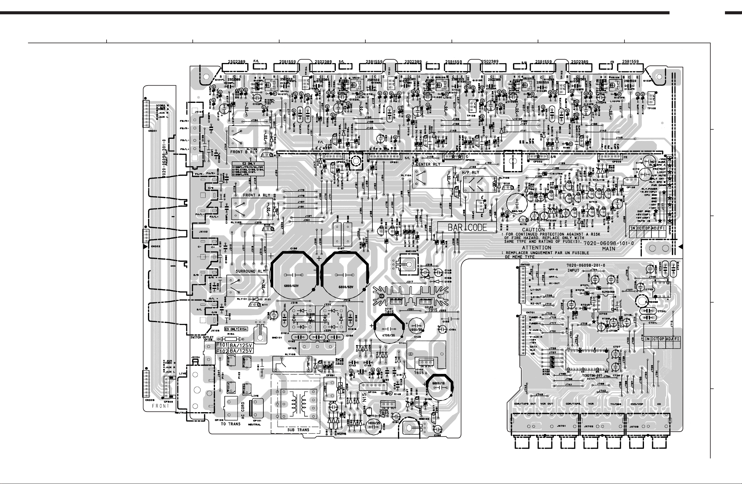
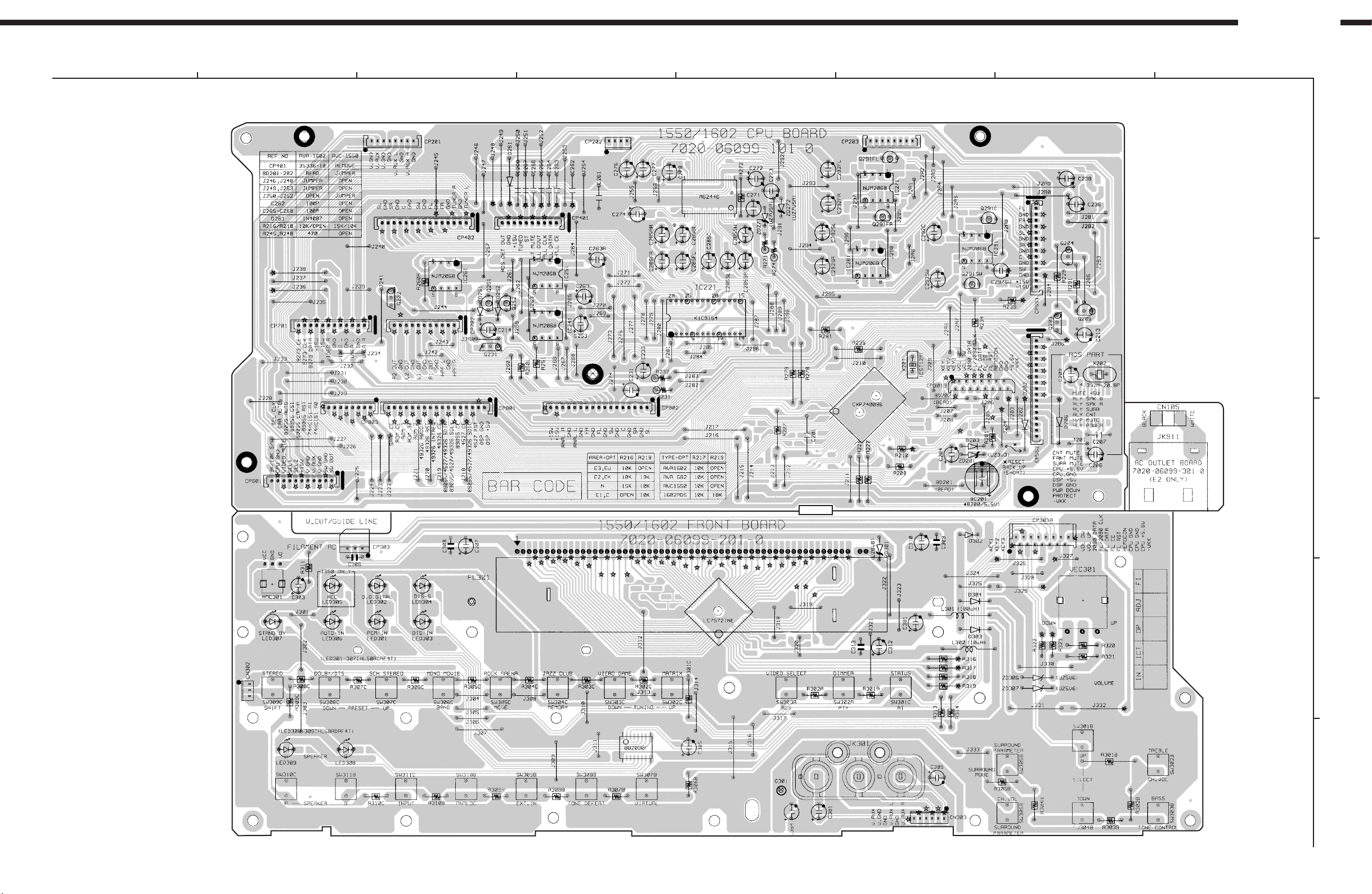
1
MAIN P.W.B. UNIT Ass'y
2
AVR-1602/682
3
4
5
76
8
1
3
1
8
1 5 1 9 1 5 1 5 1
1
3
1
3
1
3
6
1
3
A
B
13
1
3
1
4
1
8
FRONT CNT P.W.B.
C
1
11
1
D
12
16
E
MAIN P.W.B.
INPUT P.W.B.
COMPONENT SIDE
16
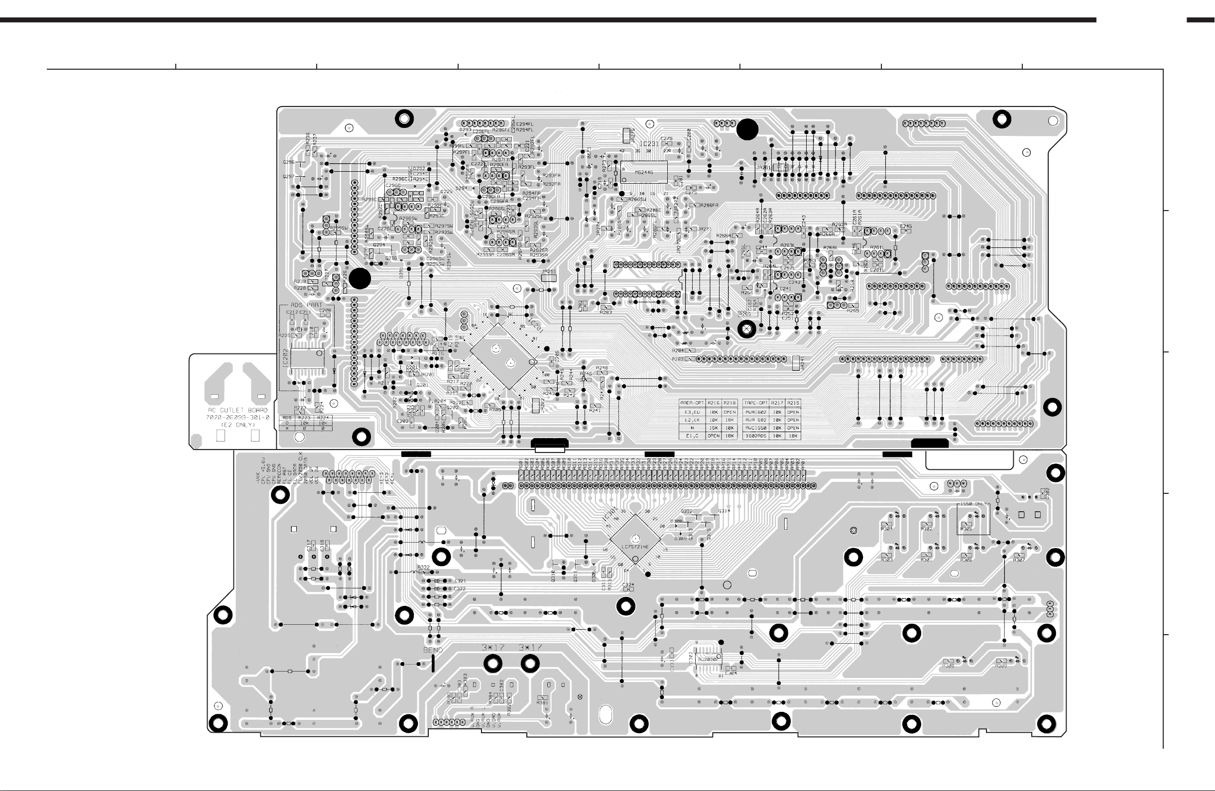
Page 17
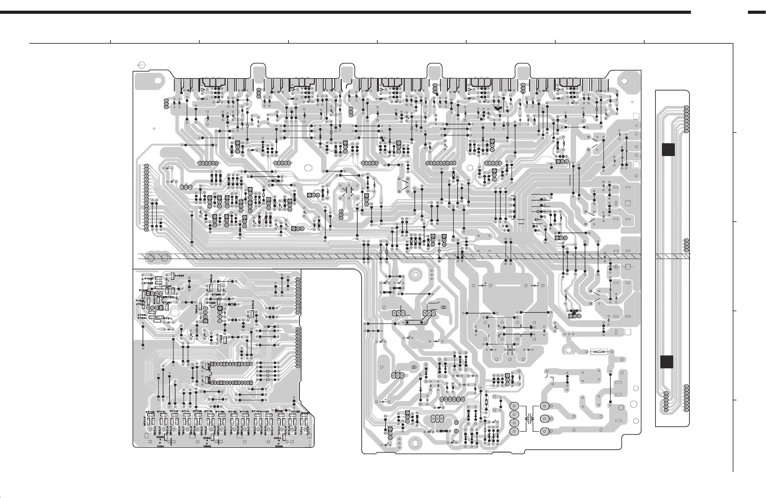
8
76
5
4
3
2
1
A
B
C
D
E
AVR-1602/682
17
FOIL SIDE
FRONT CNT P.W.B.
MAIN P.W.B.
INPUT P.W.B.
Page 18
1 8
1 1
1 4
1015
121
42
1 8
22
1
2
15
16
16
1 8
16 9
13
11711718
111
112
111
8
76
5
4
3
2
1
A
B
C
D
E
AVR-1602/682
18
CPU P.W.B. UNIT Ass'y
COMPONENT SIDE
CPU P.W.B
FRONT P.W.B
AC OUTLET P.W.B
(E2 ONLY)
Page 19
110
2011
8
76
5
4
3
2
1
A
B
C
D
E
AVR-1602/682
19
FOIL SIDE
CPU P.W.B
FRONT P.W.B
AC OUTLET P.W.B
(E2 ONLY)
Page 20
8
76
5
4
3
2
1
A
B
C
D
E
AVR-1602/682
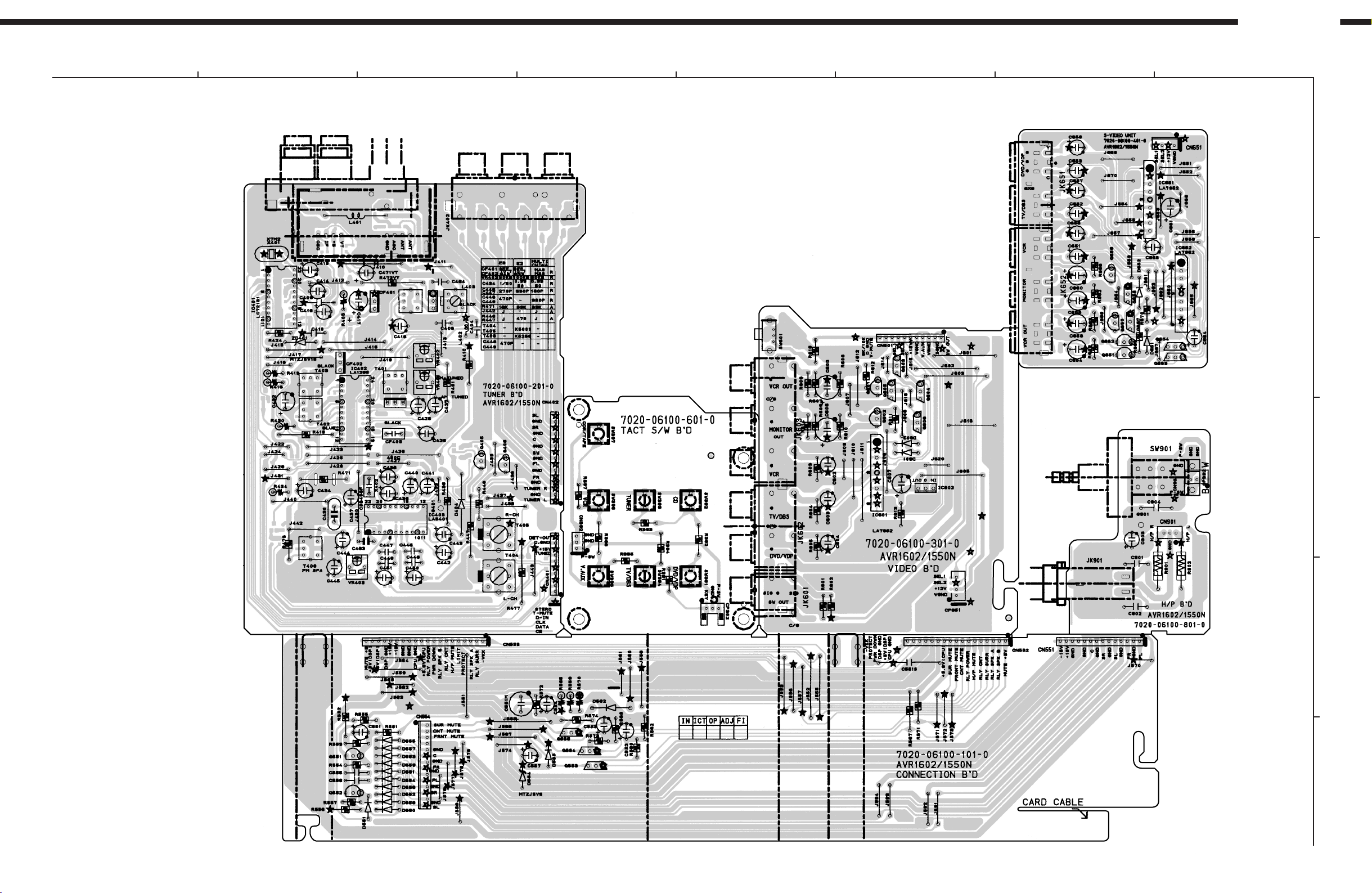
20
CONNECTION P.W.B. UNIT Ass'y
COMPONENT SIDE
TUNER P.W.B.
TACT S/W P.W.B.
VIDEO P.W.B.
S-VIDEO P.W.B.
H/P P.W.B.
CONNECTION P.W.B.
Page 21
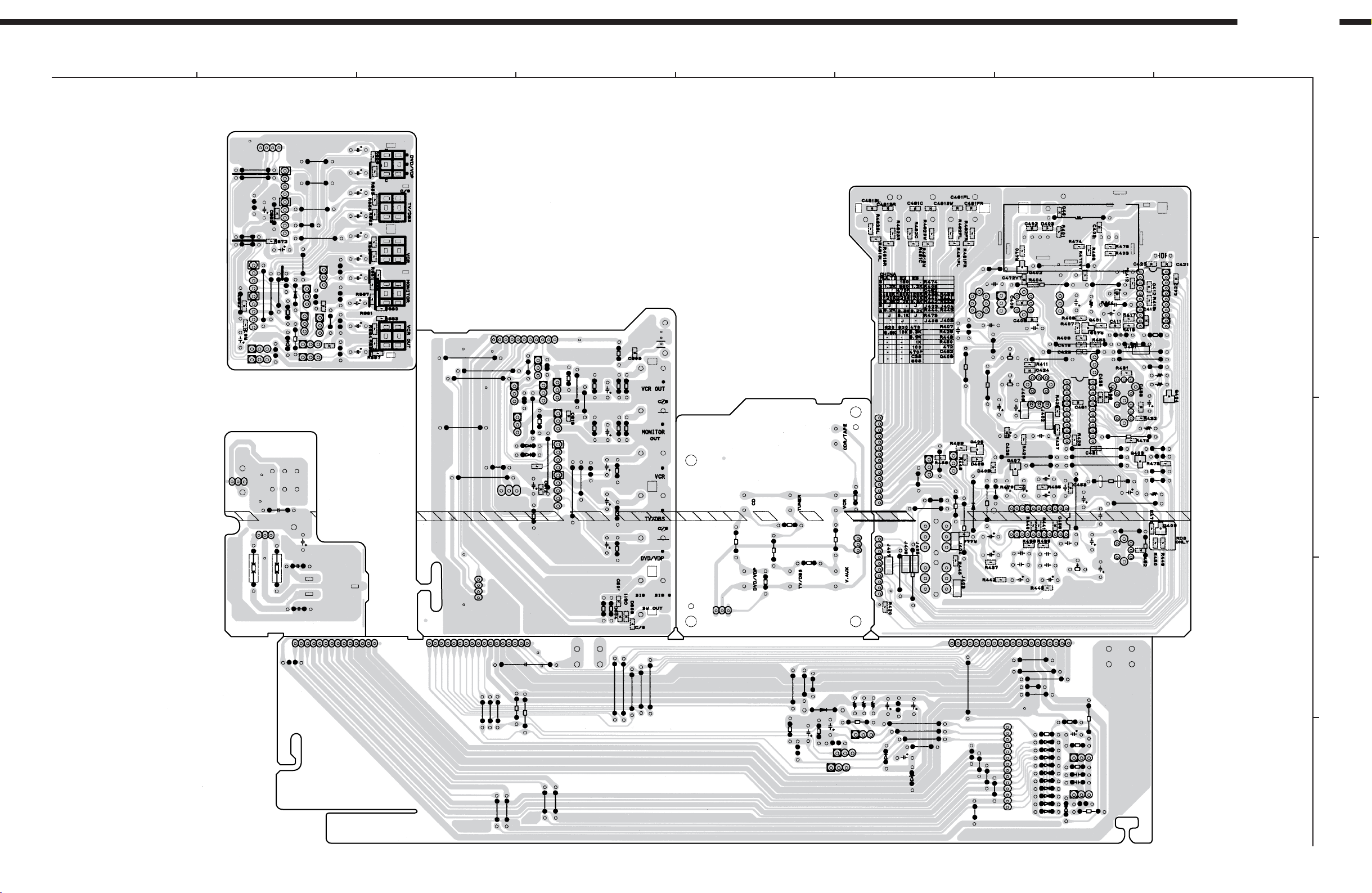
8
76
5
4
3
2
1
A
B
C
D
E
AVR-1602/682
21
FOIL SIDE
TUNER P.W.B.
TACT S/W P.W.B.
VIDEO P.W.B.
S-VIDEO P.W.B.
H/P P.W.B.
CONNECTION P.W.B.
Page 22
1
8
1 5 1 9 1 5 1 5 1 6
8
76
5
4
3
2
1
A
B
C
D
E
AVR-1602/682
22
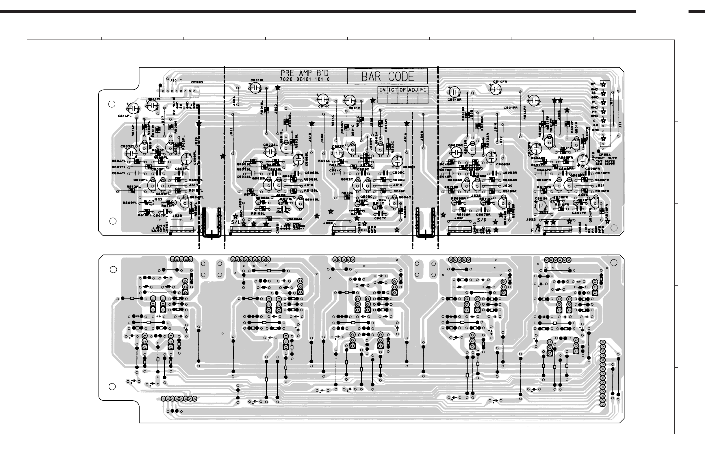
PRE AMP P.W.B. UNIT Ass'y
FOIL SIDE
COMPONENT SIDE
Page 23
1
1 10
1
17
1
17
14
15 28
1
4
8
5
1
4
8
5
1
4
8
5
1
4
85
1
4
8
5
1
8
16
9
1
7
14
1
10
20
11
8
1
12
1324
25
36
37
48
1
8
16
9
1 7
14 8
1
10
20
11
1
10
20
11
1
10
11
20
8
76
5
4
3
2
1
A
B
C
D
E
AVR-1602/682
23
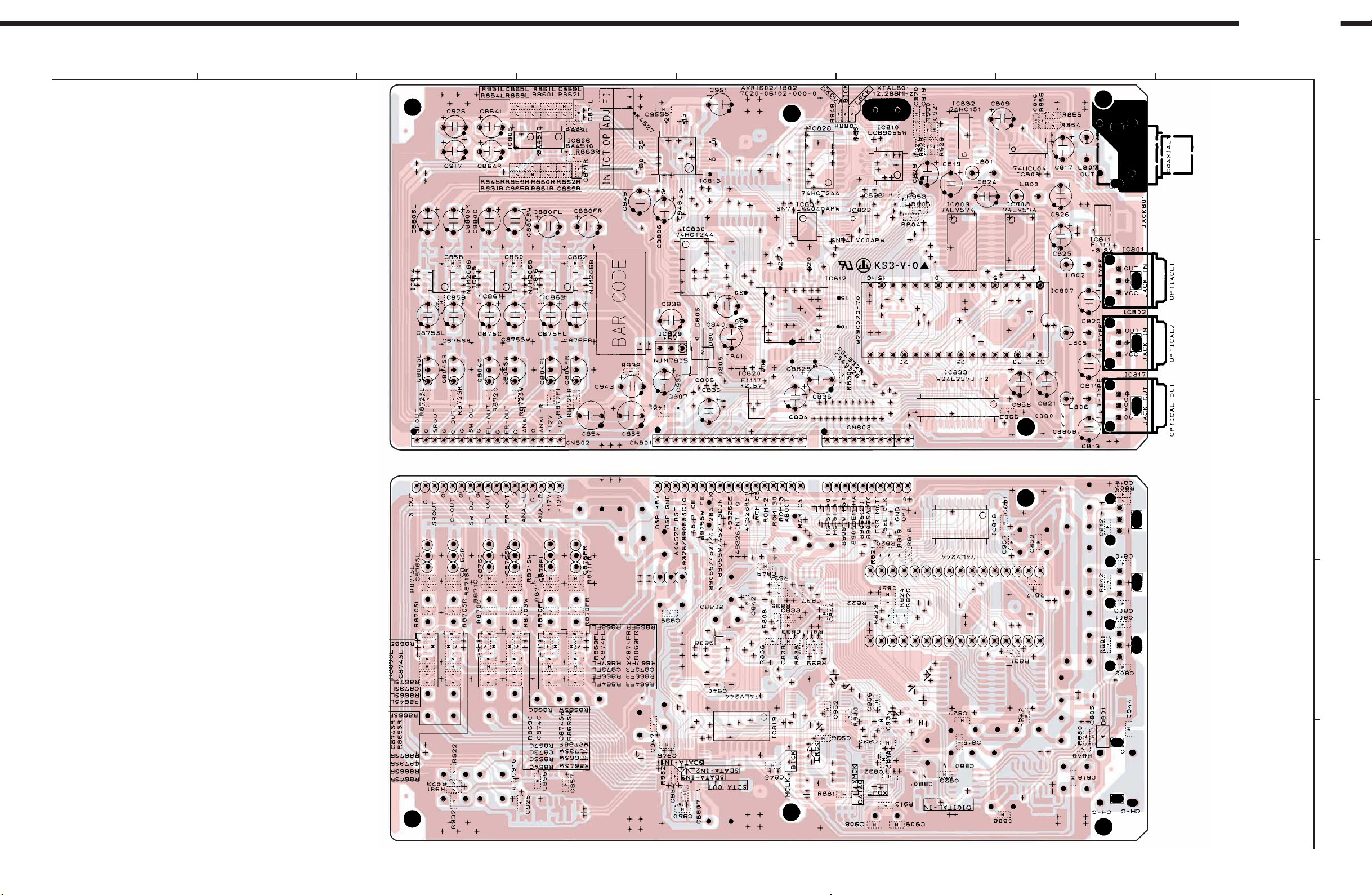
DSP P.W.B. UNIT Ass'y
FOIL SIDE
COMPONENT SIDE
10
11
1
20
10
11
1
20
Page 24
AVR-1602/682
4
32
1
A
B
C
D
E
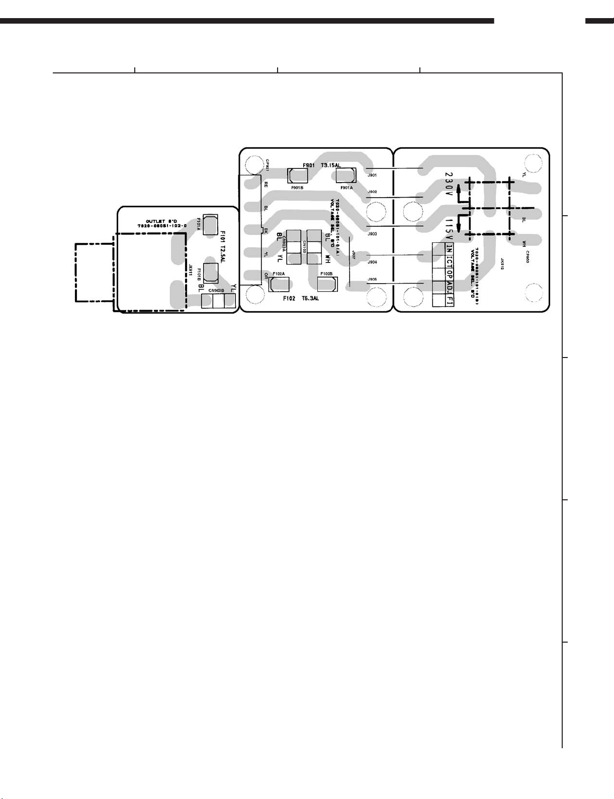
VOLTAGE SEL P.W.B. UNIT Ass'y
24
COMPONENT SIDE
Page 25
NOTE FOR PARTS LIST
l Part indicated with the mark "" are not always in stock and possibly to take a long period of time for supplying, or in
some case supplying of part may be refused.
l When ordering of part, clearly indicate "1" and "I" (i) to avoid mis-supplying.
l Ordering part without stating its part number can not be supplied.
l Part indicated with the mark "
l Not including Carbon Film ±5%, 1/4W Type in the P.W.Board parts list. (Refer to the Schematic Diagram for those parts.)
WARNING:
Parts marked with this symbol
Use ONLY replacement parts recommended by the manufacturer.
" is not illustrated in the exploded view.
have critical characteristics.
AVR-1602/682
ll
l Resistors
ll
RN 14K 2E 182 G FR
Ex.:
Type Shape Power Resist- Allowable Others
and per- ance error
formance
t
RD : Carbon 2B : 1/8W F : ±1% P : Pulse-resistant type
RC : Composition 2E : 1/4W G : ±2% NL : Low noise type
RS : Metal oxide film 2H : 1/2W J : ±5% NB : Non-burning type
RW : Winding 3A : 1W K : ±10% FR : Fuse-resistor
RN : Metal film 3D : 2W M : ±20% F : Lead wire forming
RK : Metal mixture 3F : 3W
t
3H : 5W
Resistance
1 8 2 ⇒ 1800 ohm = 1.8 kohm
s
s
• Units: ohm
1 R 2 ⇒ 1.2 ohm
s
s
• Units: ohm
Indicates number of zeros after effective number.
2-digit effective number.
1-digit effective number.
2-digit effective number, decimal point indicated by R.
t
t
ll
l Capacitors
ll
CE 04W 1H 2R2 M BP
Ex.:
Type Shape Dielectric Capacity Allowable Others
and per- strength error
formance
t
CE : Aluminum foil 0J : 6.3V F : ±1% HS : High stability type
electrolytic
CA : Aluminum solid 1A : 10V G : ±2% BP : Non-polar type
electrolytic
CS : Tantalum electrolytic 1C : 16V J : ±5% HR : Ripple-resistant type
CQ : Film 1E : 25V K : ±10% DL : For change and discharge
CK : Ceramic 1V : 35V M : ±20% HF : For assuring high
CC : Ceramic 1H : 50V Z : +80% U : UL par t
CP : Oil 2A : 100V –20% C : CSA part
CM : Mica 2B : 125V P : +100% W : UL-CSA type
CF : Metallized 2C : 160V –0% F : Lead wire forming
CH : Metallized 2D : 200V C : ±0.25pF
t
2E : 250V D : ±0.5pF
2H : 500V = : Others
2J : 630V
t
Capacity (electrolyte only)
2 2 2 ⇒ 2200µF
s
s
• Units: µF.
2 R 2 ⇒ 2.2µF
s
s
• Units: µF.
Indicates number of zeros after effective number.
2-digit effective number.
1-digit effective number.
2-digit effective number, decimal point indicated by R.
Capacity (except electrolyte)
2 2 2 ⇒ 2200pF=0.0022µF
s
s
(More than 2) Indicates number of zeros after effective number.
• Units: pF.
2 2 1 ⇒ 220pF
s
s
(0 or 1) Indicates number of zeros after effective number.
• Units: pF.
• When the dielectric strength is indicated in AC, "AC" is included after the dieelectric
strength value.
2-digit effective number.
2-digit effective number.
t
requency
25
Page 26

AVR-1602/682
Note : The symbols in the column “Remarks” indicate the following destinations.
PARTS LIST OF P.W.B. UNIT ASS'Y
MAIN P.W.B. ASS'Y
Ref. No. Part No. Part Name Remarks Ref. No. Part No. Part Name Remarks
SEMICONDUCTORS GROUP
IC101 963 0057 903 IC KIA7815AP
IC102 963 0044 806 IC NJM7915FA
IC103 960 0196 001 IC NJM7805FA
IC104 963 0057 709 IC KIA7805AP
IC105 960 0195 808 IC ICP-N15
IC701 960 0174 308 IC TC9273N-007
IC702,703 960 0179 701 IC NJM2068DD
Q104C 960 0196 506 Transistor KSC1845F
Q104FL,104FR
Q104SL,104SR
Q111-115 960 0196 904 Transistor DTC114YS
Q116 960 0196 409 Transistor 2SC1740SR
Q117 960 0196 904 Transistor DTC114YS
Q151 960 0196 409 Transistor 2SC1740SR
Q171 960 0005 202 Transistor KTC3198Y
Q171A-171C
Q172-177 960 0005 202 Transistor KTC3198Y
Q178 960 0005 105 Transistor KTA1266Y
Q179 960 0189 005 Transistor KSA916Y
Q180,181 960 0196 302 Transistor KTA1268BL
D101-105 963 0020 309 Diode 1SS133T
D121-126 963 0020 309 Diode 1SS133T
D131A,131B
D132 963 0020 309 Diode 1SS133T
D133,134 963 0046 202 Diode MTZJ18B
D135 963 0020 309 Diode 1SS133T
D136 963 0058 504 Diode MTZJ11B
D137 963 0020 309 Diode 1SS133T
D138 963 0058 407 Diode 1N4007
D141-146 963 0058 407 Diode 1N4007
D148 963 0020 309 Diode 1SS133T
D149,150 963 0058 407 Diode 1N4007
D151 963 0020 309 Diode 1SS133T
D152,153 963 0058 407 Diode 1N4007
D154 963 0047 405 Diode MTZJ7.5B
D157 963 0058 708 Diode MTZJ20B
D158-160 963 0020 309 Diode 1SS133T
RESISTORS GROUP
R104C 244 2052 957 Metal film 5.6 kohm 1W
R104FL,104FR
R104SL,104SR
R105C 244 2052 957 Metal film 5.6 kohm 1W
R105FL,105FR
R105SL,105SR
R106C 244 2051 987 Metal film 4.7 ohm 1W
R106FL,106FR
960 0196 506 Transistor KSC1845F
960 0196 506 Transistor KSC1845F
960 0196 302 Transistor KTA1268BL
960 0197 107 Diode KBPC604
244 2052 957 Metal film 5.6 kohm 1W
244 2052 957 Metal film 5.6 kohm 1W
244 2052 957 Metal film 5.6 kohm 1W
244 2052 957 Metal film 5.6 kohm 1W
244 2051 987 Metal film 4.7 ohm 1W
E3: U.S.A. & Canada model EU: U.S.A. model (AVR-682)
E2: Europe model E1: Asia model
E1C: China model E1H: Hong Kong model
E1T: Taiwan R.O.C. model
R106SL,106SR
R107C 244 2051 987 Metal film 4.7 ohm 1W
R107FL,107FR
R107SL,107SR
R108C 244 2043 982 Metal film 0.22 ohm 1W
R108FL,108FR
R108SL,108SR
R109C 244 2043 982 Metal film 0.22 ohm 1W
R109FL,109FR
R109SL,109SR
R110C 244 2043 982 Metal film 0.22 ohm 1W
R110FL,110FR
R110SL,110SR
R111C 244 2043 982 Metal film 0.22 ohm 1W
R111FL,111FR
R111SL,111SR
R118C 244 2043 937 Metal oxide 10 ohm 1W(NB)
R118FL,118FR
R118SL,118SR
R119C 244 2043 937 Metal oxide 10 ohm 1W(NB)
R119FL,119FR
R119SL,119SR
R135,136 963 0045 203 Winding 0.1 ohm 5W
R141,142 244 2043 982 Metal film 0.22 ohm 1W
R148,149 244 2043 982 Metal film 0.22 ohm 1W
R151 963 9003 343 Metal film 68 ohm 1/4W
R154 963 0043 108 Metal film 2.2 Mohm 1/2W for E3,EU
R155,156 963 9003 039 Metal film 1 ohm 1/4W
R179 963 9003 055 Metal film 47 kohm 1/4W
R181 244 2051 987 Metal film 4.7 ohm 1W
R184 244 2043 937 Metal oxide 10 ohm 1W(NB)
R185 963 9003 039 Metal film 1 ohm 1/4W
R701L,701R
R702L,702R
R703L,703R
R704L,704R
R705L,705R
R706L,706R
R707L,707R
R710L,710R
R711L,711R
R712L,712R
R713L,713R
R714L,714R
R715L,715R
R716L,716R
R725L,725R
R726L,726R
R728L,728R
R729L,729R
R730L,730R
244 2051 987 Metal film 4.7 ohm 1W
244 2051 987 Metal film 4.7 ohm 1W
244 2051 987 Metal film 4.7 ohm 1W
244 2043 982 Metal film 0.22 ohm 1W
244 2043 982 Metal film 0.22 ohm 1W
244 2043 982 Metal film 0.22 ohm 1W
244 2043 982 Metal film 0.22 ohm 1W
244 2043 982 Metal film 0.22 ohm 1W
244 2043 982 Metal film 0.22 ohm 1W
244 2043 982 Metal film 0.22 ohm 1W
244 2043 982 Metal film 0.22 ohm 1W
244 2043 937 Metal oxide 10 ohm 1W(NB)
244 2043 937 Metal oxide 10 ohm 1W(NB)
244 2043 937 Metal oxide 10 ohm 1W(NB)
244 2043 937 Metal oxide 10 ohm 1W(NB)
963 9004 339 Carbon chip 470 ohm 1/16W
963 9004 339 Carbon chip 470 ohm 1/16W
963 9004 339 Carbon chip 470 ohm 1/16W
963 9004 339 Carbon chip 470 ohm 1/16W
963 9004 339 Carbon chip 470 ohm 1/16W
963 9004 339 Carbon chip 470 ohm 1/16W
963 9004 339 Carbon chip 470 ohm 1/16W
963 9004 245 Carbon chip 2.2 Mohm 1/16W
963 9004 245 Carbon chip 2.2 Mohm 1/16W
963 9004 245 Carbon chip 2.2 Mohm 1/16W
963 9004 245 Carbon chip 2.2 Mohm 1/16W
963 9004 245 Carbon chip 2.2 Mohm 1/16W
963 9004 245 Carbon chip 2.2 Mohm 1/16W
963 9004 245 Carbon chip 2.2 Mohm 1/16W
960 9003 385 Carbon chip 100 ohm 1/16W
963 9004 083 Carbon chip 100 kohm 1/16W
963 9004 300 Carbon chip 39 kohm 1/16W
963 9003 385 Carbon chip 100 ohm 1/16W
963 9004 083 Carbon chip 100 kohm 1/16W
26
Page 27

AVR-1602/682
Ref. No. Part No. Part Name Remarks Ref. No. Part No. Part Name Remarks
R731L,731R
R732L,732R
R751L,751R
963 9004 300 Carbon chip 39 kohm 1/16W
963 9004 300 Carbon chip 39 kohm 1/16W
963 9004 083 Carbon chip 100 kohm 1/16W
C198FL,198FR
C198SL,198SR
C199FL,199FR
960 9006 202 Ceramic 0.01uF/50V for E2
960 9006 202 Ceramic 0.01uF/50V for E2
960 9006 202 Ceramic 0.01uF/50V for E2
VR101-105 960 0091 601 Semi fixed resistor 1 kohm
CAPACITORS GROUP
C101C Electrolytic 47uF/50V
C101FL,101FR
C101SL,101SR
C102C Electrolytic 10uF/35V
C102FL,102FR
C102SL,102SR
C103C 963 9003 084 Ceramic 100pF/500V
C103FL,103FR
C103SL,103SR
C104C 963 9003 084 Ceramic 100pF/500V
C104FL,104FR
C104SL,104SR
C105C 960 9003 108 Ceramic 0.022uF/25V
C105FL,105FR
C105SL,105SR
C107C 963 9003 097 Mylar film 0.1uF/250V
C107FL,107FR
C107SL,107SR
C131-135 963 9003 097 Mylar film 0.1uF/250V
C136,137 963 0087 203 Electrolytic 10000uF/63V
C138 Electrolytic 1uF/50V
C141-143 963 0021 900 Mylar film 0.047uF/100V
C144 963 9003 110 Electrolytic 4700uF/35V
C145 963 9003 123 Electrolytic 1000uF/35V
C146 Electrolytic 1uF/50V
C148 Electrolytic 1uF/50V
C150-152 963 0021 900 Mylar film 0.047uF/100V
C153 963 0021 104 Electrolytic 6800uF/16V
C154 Electrolytic 10uF/35V
C155 963 0020 202 Ceramic 0.1uF/50V
C157 Electrolytic 1uF/50V
C158 963 9003 136 Electrolytic 1000uF/25V
C159 Electrolytic 1uF/50V
C161 Electrolytic 10uF/35V
C171 Electrolytic 100uF/10V
C171A-171C
C172,173 Electrolytic 220uF/6.3V
C174 Electrolytic 10uF/35V
C175 Electrolytic 4.7uF/50V
C176,177 Electrolytic 1uF/50V
C178 963 9003 149 Electrolytic 330uF/63V
C181 963 0076 104 Ceramic 4700pF/250V(AC)
C182 963 9004 795 Electrolytic 10uF/100V
C191-197 Ceramic 2200pF/16V for E2
C198C 960 9006 202 Ceramic 0.01uF/50V for E2
963 9003 084 Ceramic 100pF/500V
963 9003 084 Ceramic 100pF/500V
963 9003 084 Ceramic 100pF/500V
963 9003 084 Ceramic 100pF/500V
960 9003 108 Ceramic 0.022uF/25V
960 9003 108 Ceramic 0.022uF/25V
963 9003 097 Mylar film 0.1uF/250V
963 9003 097 Mylar film 0.1uF/250V
963 0020 202 Ceramic 0.1uF/50V
Electrolytic 47uF/50V
Electrolytic 47uF/50V
Electrolytic 10uF/35V
Electrolytic 10uF/35V
C701L,701R
C702L,702R
C703L,703R
C704L,704R
C705L,705R
C706L,706R
C707L,707R
C716L,716R
C718L,718R
C719L,719R
C720L,720R
C721L,721R
C723L,723R
C724L,724R
C725,726 963 9004 698 Ceramic chip 0.01uF/50V
C727,728 Electrolytic 10uF/35V
OTHER PARTS GROUP
CN201 963 0046 309 8P connector base 1
CN202 963 0075 707 4P connector base 1
CN203 963 0046 309 8P connector base 1
CN701 960 0117 103 12P connector base 1
CN702 963 0046 600 11P connector base
CP101 960 0197 505 2P connector base 1
CP102 960 0123 304 2P connector base
CP102 963 0066 208 3P connector base for E1,E1H,E1T 1
CP103 963 0066 208 3P connector base 1
CP104 960 0128 804 6P connector base 1
CP105 960 0123 304 2P connector base
CP106 960 0123 207 3P connector base 1
CP303 963 0075 600 6P connector base 1
CP501 963 0046 901 9P connector base 1
CP502-504 963 0048 608 5P connector base 3
CP505 963 0049 500 6P connector base 1
CP553 963 0048 802 20P connector base 1
CP901 963 0048 909 3P connector base 1
CP931 960 0123 304 2P connector base
F101 960 0188 705 Fuse 125V-8A for E3,EU 1
F101 960 0142 602 Fuse 250V-T2.5A for E2 1
F101A,101B
F102 960 0188 705 Fuse 125V-8A for E3,EU 1
F102 963 0044 709 Fuse 250V-T3.15A for E2,E1C 1
F102A,102B
GND101-103
963 9004 575 Ceramic chip 100pF/50V for E2
963 9004 575 Ceramic chip 100pF/50V for E2
963 9004 575 Ceramic chip 100pF/50V for E2
963 9004 575 Ceramic chip 100pF/50V for E2
963 9004 575 Ceramic chip 100pF/50V for E2
963 9004 575 Ceramic chip 100pF/50V for E2
963 9004 575 Ceramic chip 100pF/50V for E2
Electrolytic 10uF/35V
Electrolytic 10uF/35V
Electrolytic 10uF/35V
963 9003 152 Mylar film 0.068uF/100V
963 9003 152 Mylar film 0.068uF/100V
Electrolytic 10uF/35V
963 9004 698 Ceramic chip 0.01uF/50V
for E3,EU,E2,E1C
for E2,E1,E1H,E1T
for E2,E1,E1C,E1H,E1T
960 0005 804 Fuse clip for E3,EU,E2 2
960 0005 804 Fuse clip
960 9006 600 Terminal 3
for E3,EU,E2,E1C
Q’ty
1
1
1
2
27
Page 28

Ref. No. Part No. Part Name Remarks
JK103 960 0194 809 2P Terminal 1
JK104 960 0181 508 AC outlet for E3,EU 1
L101C 963 0049 005 Inductor 0.5uH 1
L101FL,101FR
L101SL,101SR
RLY101-104
963 0049 005 Inductor 0.5uH 2
963 0049 005 Inductor 0.5uH 2
960 0181 702 Relay G5PA-28 24V 5A 4
RLY105 963 0071 303 Relay RSB24S 24V 2A30VDC 1
RLY106 960 0181 605 Relay G5PA-1-8 12V 5A 1
TP101-105 960 0161 405 3P connector base 5
Heat sink 1
Heat sink 1
963 0068 400 Condenser cover
for E2,E1,E1C,E1H,E1T
963 0060 000 Fuse label F101 for E2 1
963 0090 504 Fuse label F102 for E1C 1
960 0185 708 Sub trans. for E3,EU 1
960 0185 711 Sub trans. for E2 1
960 0185 737 Sub trans. for E1,E1H,E1T 1
960 0185 724 Sub trans. for E1C 1
963 0018 007 Screw 3x8 CBTS(B) 3
960 0158 308 4P Terminal 1
963 0074 009 8P Terminal 1
960 0194 702 4P pin jack 2
960 0188 307 6P pin jack 1
Note : The symbols in the column “Remarks” indicate the following destinations.
E3: U.S.A. & Canada model EU: U.S.A. model (AVR-682)
E2: Europe model E1: Asia model
E1C: China model E1H: Hong Kong model
E1T: Taiwan R.O.C. model
CPU P.W.B. ASS'Y
Q’ty
Ref. No. Part No. Part Name Remarks
SEMICONDUCTORS GROUP
IC201 963 0084 303 IC CXP740096-135Q
IC202 963 0057 602 IC TDA7330BD for E2
IC221 963 0080 201 IC KIC9164AN
IC231 960 0179 604 IC M62446FP
IC241 960 0179 701 IC NJM2068DD
IC251 960 0179 701 IC NJM2068DD
IC261 960 0179 701 IC NJM2068DD
IC271 960 0179 701 IC NJM2068DD
IC281 960 0179 701 IC NJM2068DD
IC291 960 0179 701 IC NJM2068DD
IC301 960 0180 004 IC LC75721E
IC302 963 0074 504 IC BU2090F
1
RMC301 960 0181 100 Remote sensor NJL64H380A
Q201 963 0075 202 Transistor DTC144EK
Q202 963 0045 902 Transistor 2SC2412K
Q203 963 0075 309 Transistor DTA114ES
Q204,205 960 0196 603 Transistor KTC2874B
Q231 963 0075 309 Transistor DTA114ES
Q232 963 0075 503 Transistor DTC144ES
Q251,252 960 0196 807 FET 2SK117Y
Q291C 960 0196 807 FET 2SK117Y
Q291FL,291FR
960 0196 807 FET 2SK117Y
Q291SW 960 0196 807 FET 2SK117Y
Q294 963 0058 203 Transistor DTA114EK
Q295 963 0075 202 Transistor DTC144EK
Q296 963 0058 203 Transistor DTA114EK
Q297 963 0075 202 Transistor DTC144EK
AVR-1602/682
Q310 963 0075 008 Transistor DTA144EK
Q311 963 0075 202 Transistor DTC144EK
Q312 963 0075 008 Transistor DTA144EK
Q313 963 0075 202 Transistor DTC144EK
Q314 963 0075 008 Transistor DTA144EK
Q315 963 0075 202 Transistor DTC144EK
D201 960 0197 000 Diode KDS160
D202 963 0058 407 Diode 1N4007
D203 963 0020 309 Diode 1SS133
D204,205 960 0197 000 Diode KDS160
D206 963 0020 309 Diode 1SS133 for E2
D251,252 963 0020 309 Diode 1SS133
D261 963 0058 407 Diode 1N4007
D291-294 960 0197 000 Diode KDS160
D302-304 963 0020 309 Diode 1SS133
D305 960 0197 000 Diode KDS160
D308,309 960 0197 000 Diode KDS160
28
Page 29

AVR-1602/682
Ref. No. Part No. Part Name Remarks Ref. No. Part No. Part Name Remarks
ZD201 963 0047 502 Zener diode MTZJ3.3B
ZD271,272 960 0222 603 Zener diode MTZJ7.5A
ZD301 960 0095 801 Zener diode MTZJ6.8B
ZD306,307 960 0095 607 Zener diode MTZJ5.6B
LED301-304
LED306-309
RESISTORS GROUP
R202 963 9003 398 Carbon chip 1 kohm 1/16W
R203,204 963 9004 342 Carbon chip 4.7 kohm 1/16W
R205 963 9004 070 Carbon chip 10 kohm 1/16W
R206 963 9004 232 Carbon chip 220 kohm 1/16W
R209 963 9004 070 Carbon chip 10 kohm 1/16W
R211 963 9004 070 Carbon chip 10 kohm 1/16W
R212 963 9003 398 Carbon chip 1 kohm 1/16W
R213-215 963 9004 122 Carbon chip 12 kohm 1/16W
R216 963 9004 070 Carbon chip 10 kohm 1/16W for E3,EU,E2
R217 963 9004 070 Carbon chip 10 kohm 1/16W for E3,EU
R218 963 9004 070 Carbon chip 10 kohm 1/16W for E1,E1C,E1H,E1T
R218,219 963 9004 177 Carbon chip 18 kohm 1/16W for E2
R220 963 9004 070 Carbon chip 10 kohm 1/16W
R223,224 963 9003 372 Carbon chip 0 ohm 1/16W
R223,224 963 9004 070 Carbon chip 10 kohm 1/16W for E2
R225 963 9004 245 Carbon chip 2.2 Mohm 1/16W for E2
R226 963 9004 070 Carbon chip 10 kohm 1/16W
R227 963 9003 398 Carbon chip 1 kohm 1/16W
R228 963 9004 368 Carbon chip 470 kohm 1/16W
R230 963 9004 229 Carbon chip 22 kohm 1/16W
R231,232 244 2051 961 Metal film 100 ohm 1W
R236 963 9004 216 Carbon chip 2.2 kohm 1/16W
R237 963 9004 070 Carbon chip 10 kohm 1/16W
R238 963 9004 216 Carbon chip 2.2 kohm 1/16W
R241-248 963 9004 339 Carbon chip 470 ohm 1/16W
R252 963 9004 449 Carbon chip 6.8 kohm 1/16W
R253 963 9004 834 Carbon chip 5.6 kohm 1/16W
R254 963 9004 481 Carbon chip 8.2 kohm 1/16W
R255 963 9003 385 Carbon chip 100 ohm 1/16W
R256 963 9004 083 Carbon chip 100 kohm 1/16W
R258 963 9004 070 Carbon chip 10 kohm 1/16W
R259 963 9004 216 Carbon chip 2.2 kohm 1/16W
R261L,261R
R262L,262R
R263L,263R
R264L,264R
R265L,265R
R266L,266R
R271 244 2051 958 Metal film 220 ohm 1W
R273 963 9005 325 Carbon chip 2.7 kohm 1/16W
R274 244 2051 958 Metal film 220 ohm 1W
R282-284 963 9003 385 Carbon chip 100 ohm 1/16W
960 0197 204 LED PI5-RD/HL50RDRF4T
960 0197 204 LED PI5-RD/HL50RDRF4T
for E3,EU,E1,E1C,E1H,E1T
963 9004 342 Carbon chip 4.7 kohm 1/16W
963 9004 151 Carbon chip 15 kohm 1/16W
963 9004 151 Carbon chip 15 kohm 1/16W
963 9003 385 Carbon chip 100 ohm 1/16W
963 9004 083 Carbon chip 100 kohm 1/16W
963 9004 410 Carbon chip 6.2 kohm 1/16W
R286C 963 9004 232 Carbon chip 220 kohm 1/16W
R286FL,286FR
R286SL,286SR
R286SW 963 9004 232 Carbon chip 220 kohm 1/16W
R292C 963 9003 385 Carbon chip 100 ohm 1/16W
R292FL,292FR
R292SL,292SR
R292SW 963 9003 385 Carbon chip 100 ohm 1/16W
R293C 963 9004 355 Carbon chip 47 kohm 1/16W
R293FL,293FR
R293SL,293SR
R293SW 963 9004 355 Carbon chip 47 kohm 1/16W
R294C 963 9004 481 Carbon chip 8.2 kohm 1/16W
R294FL,294FR
R294SW 963 9005 338 Carbon chip 16 kohm 1/10W
R295SW 963 9004 355 Carbon chip 47 kohm 1/16W
R296C 963 9005 341 Carbon chip 13 kohm 1/10W
R296FL,296FR
R296SL,296SR
R296SW 963 9004 122 Carbon chip 12 kohm 1/16W
R297C 963 9004 216 Carbon chip 2.2 kohm 1/16W
R297FL,297FR
R297SL,297SR
R297SW 963 9005 008 Carbon chip 620 ohm 1/16W
R298SW 963 9004 083 Carbon chip 100 kohm 1/16W
R299C 963 9004 339 Carbon chip 470 ohm 1/16W
R299FL,299FR
R299SL,299SR
R299SW 963 9003 398 Carbon chip 1 kohm 1/16W
R301-304 963 9004 436 Carbon chip 680 ohm 1/16W
R306-309 963 9004 436 Carbon chip 680 ohm 1/16W
R315 963 9004 070 Carbon chip 10 kohm 1/16W
R332 963 9004 342 Carbon chip 4.7 kohm 1/16W
R381 963 9004 465 Carbon chip 75 ohm 1/16W
R382,383 963 9004 339 Carbon chip 470 ohm 1/16W
R384,385 963 9004 245 Carbon chip 2.2 Mohm 1/16W
RG01 963 9004 397 Carbon chip 56 kohm 1/16W
RP01-38 963 9004 397 Carbon chip 56 kohm 1/16W
CAPACITORS GROUP
BC201 963 0061 504
C201 963 9004 546 Ceramic 0.01uF/16V
C202 963 9004 711 Ceramic chip 0.1uF/50V
C203 963 9004 698 Ceramic chip 0.01uF/50V
C204 Electrolytic 4.7uF/50V
C205 963 9004 711 Ceramic chip 0.1uF/50V
C206 Electrolytic 47uF/10V for E2
C207 963 9004 546 Ceramic 0.01uF/16V for E2
963 9004 232 Carbon chip 220 kohm 1/16W
963 9004 232 Carbon chip 220 kohm 1/16W
963 9003 385 Carbon chip 100 ohm 1/16W
963 9003 385 Carbon chip 100 ohm 1/16W
963 9004 355 Carbon chip 47 kohm 1/16W
963 9004 355 Carbon chip 47 kohm 1/16W
963 9004 371 Carbon chip 5.1 kohm 1/16W
963 9004 834 Carbon chip 5.6 kohm 1/16W
963 9005 341 Carbon chip 13 kohm 1/10W
963 9003 398 Carbon chip 1 kohm 1/16W
963 9004 216 Carbon chip 2.2 kohm 1/16W
963 9004 339 Carbon chip 470 ohm 1/16W
963 9004 339 Carbon chip 470 ohm 1/16W
Electric double layer 8200uF/5.5V
29
Page 30

AVR-1602/682
Ref. No. Part No. Part Name Remarks Ref. No. Part No. Part Name Remarks
C208 963 9005 354 Ceramic chip 270pF/50V for E2
C209 Electrolytic 10uF/35V for E2
C210 963 9004 698 Ceramic chip 0.01uF/50V for E2
C211,212 963 9004 614 Ceramic chip 27pF/50V for E2
C213 Electrolytic 0.1uF/50V
C214 Electrolytic 1uF/50V
C219-226 963 9004 753 Ceramic chip 0.047uF/50V
C231 Electrolytic 47uF/25V
C233 Electrolytic 47uF/25V
C236 Electrolytic 47uF/25V
C238 Electrolytic 47uF/25V
C241-246 963 9004 753 Ceramic chip 0.047uF/50V
C251 963 9004 575 Ceramic chip 100pF/50V
C252 963 9004 643 Ceramic chip 47pF/50V
C253 Electrolytic 10uF/35V
C261-268 963 9004 520 Ceramic 100pF/50V
C261L,261R
C262L,262R
C263L,263R
C271 Electrolytic 47uF/10V
C272 Electrolytic 1uF/50V
C273 Electrolytic 47uF/10V
C274 Electrolytic 0.33uF/50V
C275 963 9005 367 Ceramic chip 0.015uF/50V
C276,277 Electrolytic 3.3uF/50V
C278 Electrolytic 0.33uF/50V
C279 963 9005 367 Ceramic chip 0.015uF/50V
C280,281 963 9005 370 Ceramic chip 8200pF/50V
C282 963 9004 575 Ceramic chip 100pF/50V
C285BL,285BR
C285C Electrolytic 4.7uF/50V
C285FL,285FR
C285SL,285SR
C285SW Electrolytic 4.7uF/50V
C292C Electrolytic 4.7uF/50V
C292FL,292FR
C292SL,292SR
C292SW Electrolytic 4.7uF/50V
C294C 963 9005 383 Ceramic chip 2700pF/50V
C294FL,294FR
C295C 963 9004 575 Ceramic chip 100pF/50V
C295FL,295FR
C296C 963 9004 630 Ceramic chip 39pF/50V
C296FL,296FR
C296SL,296SR
C296SW 963 9004 575 Ceramic chip 100pF/50V
C297SW Electrolytic 4.7uF/50V
C301 Electrolytic 10uF/50V
C302 963 9004 753 Ceramic chip 0.047uF/50V
C303 Electrolytic 47uF/10V
C304 963 9004 737 Ceramic chip 0.022uF/25V
963 9004 575 Ceramic chip 100pF/50V
963 9004 627 Ceramic chip 33pF/50V
Electrolytic 10uF/35V
Electrolytic 4.7uF/50V
Electrolytic 4.7uF/50V
Electrolytic 4.7uF/50V
Electrolytic 10uF/35V
Electrolytic 10uF/35V
963 9005 396 Ceramic chip 4700pF/50V
963 9004 672 Ceramic chip 680pF/50V
963 9005 422 Ceramic chip 82pF/50V
963 9004 630 Ceramic chip 39pF/50V
C305 Electrolytic 47uF/16V
C306 963 9004 766 Mylar film 0.1uF/100V
C307 Electrolytic 1uF/50V
C308,309 963 0021 900 Mylar film 0.047uF/100V
C310 Electrolytic 1uF/50V
C311 963 9005 406 Ceramic chip 30pF/50V
C312 Electrolytic 47uF/16V
C313 963 9005 419 Mylar film 0.047uF/63V
C316,317 963 9004 698 Ceramic chip 0.01uF/50V
C321 963 9004 685 Ceramic chip 1000pF/50V
C322 963 9004 575 Ceramic chip 100pF/50V
C324 963 9004 575 Ceramic chip 100pF/50V
C333 963 9004 575 Ceramic chip 100pF/50V
C381 Electrolytic 47uF/10V
C382,383 963 9004 575 Ceramic chip 100pF/50V
C384,385 Electrolytic 1uF/50V
OTHER PARTS GROUP
BD201,202 963 0053 800 Beads inductor 2
CN105 963 0089 405 2P connector cord for E2 1
CN302 963 0087 300 3P connector cord 1
CN303 963 0090 407 6P connector cord 1
CP201 963 0046 804 8P connector base 1
CP202 963 0075 804 4P connector base 1
CP203 963 0046 804 8P connector base 1
CP301A 963 0075 901 15P FPC base 1
CP301B 960 0217 524 15P FPC base 1
CP303 963 0049 102 3P connector base 1
CP401 963 0047 007 10P connector base 1
CP402 963 0049 209 15P connector base 1
CP551 960 0123 003 14P connector base 1
CP552 963 0049 306 17P connector base 1
CP601 963 0047 104 11P connector base 1
CP701 960 0116 803 12P connector base 1
CP702 963 0047 104 11P connector base 1
CP801,802 963 0049 306 17P connector base 2
CP803 963 0046 804 8P connector base 1
FL301 960 0180 509 FLT 16-ST-42GNK 1
G301
JK301 963 0067 508 3P pin jack 1
L301 960 0128 008 Inductor 100uH 1
L302 960 0010 307 Inductor 10uH 1
SW301B,301C
SW302A-302C
SW303A-303C
963 0045 708 Tact switch 2
963 0045 708 Tact switch 3
963 0045 708 Tact switch 3
1P lug wire L60 BK 1
Q’ty
30
Page 31

Ref. No. Part No. Part Name Remarks
SW304B,304C
SW305B,305C
SW306B,306C
SW307B,307C
SW308B,308C
SW309B,309C
SW310B,310C
SW311B,311C
963 0045 708 Tact switch 2
963 0045 708 Tact switch 2
963 0045 708 Tact switch 2
963 0045 708 Tact switch 2
963 0045 708 Tact switch 2
963 0045 708 Tact switch 2
963 0045 708 Tact switch 2
963 0045 708 Tact switch 2
Note : The symbols in the column “Remarks” indicate the following destinations.
E3: U.S.A. & Canada model EU: U.S.A. model (AVR-682)
E2: Europe model E1: Asia model
E1C: China model E1H: Hong Kong model
E1T: Taiwan R.O.C. model
CNT P.W.B. ASS'Y
Q’ty
Ref. No. Part No. Part Name Remarks
SEMICONDUCTORS GROUP
IC401 963 0043 700 IC LC72131
IC402 963 0043 904 IC LA1266
IC403 963 0044 000 IC LA3401
IC601 960 0180 101 IC LA7952
IC602 963 0074 902 IC NJM7812FA
IC651,652 960 0180 101 IC LA7952
AVR-1602/682
for E3,EU,E1,E1C,E1H,E1T
VEC301 960 0181 207 Encoder EC16B2420431 1
X201 960 0181 003
Ceramic resonator CST12.0MTW
X202 960 0091 818 Crystal 4.332MHz for E2 1
960 0184 408 FLT holder 1
960 0143 203 AC outlet for E2 1
Wire clamp
for E3,EU,E1,E1C,E1H,E1T
Q401 963 0058 300 Transistor KTC3880S
Q402 963 0075 105 Transistor DTC114EK
1
Q403,404 963 0058 203 Transistor DTA114EK
Q405,406 960 0196 603 Transistor KTC2874B
Q407 963 0024 208 Transistor DTC114YK
Q408 963 0058 203 Transistor DTA114EK
Q409 963 0058 300 Transistor KTC3880S for E2
2
Q551 960 0196 700 Transistor KTC3200BL
Q552 960 0196 302 Transistor KTA1268BL
Q553-555 963 0075 309 Transistor DTA114ES
Q601,602 960 0096 800 Transistor 2SC3199Y
Q603,604 960 0196 904 Transistor DTC114YS
Q605,606 963 0075 406 Transistor DTC114TS
Q651,652 960 0096 800 Transistor 2SC3199Y
Q653,654 960 0196 904 Transistor DTC114YS
Q655,656 960 0096 800 Transistor 2SC3199Y
Q657,658 960 0196 904 Transistor DTC114YS
D403 960 0197 000 Diode KDS160
D404 963 0020 309 Diode 1SS133
D405,406 960 0197 000 Diode KDS160
for E3,EU,E1,E1C,E1H,E1T
for E3,EU,E1,E1C,E1H,E1T
for E3,EU,E1,E1C,E1H,E1T
for E3,EU,E1,E1C,E1H,E1T
D551-561 963 0020 309 Diode 1SS133
D562 963 0058 407 Diode 1N4007
D564 960 0095 607 Zener diode MTZJ5.6B
D565 963 0020 309 Diode 1SS133
D601,602 963 0020 309 Diode 1SS133
D651,652 963 0020 309 Diode 1SS133
for E3,EU,E1,E1C,E1H,E1T
ZD401 960 0095 500 Zener diode MTZJ5.1B
RESISTORS GROUP
R401 963 9004 821 Carbon chip 10 ohm 1/16W
R403 963 9004 339 Carbon chip 470 ohm 1/16W
R404 963 9004 083 Carbon chip 100 kohm 1/16W
R405 960 9003 807 Metal film 100 ohm 1/4W
R406 963 9004 342 Carbon chip 4.7 kohm 1/16W
R407 963 9004 339 Carbon chip 470 ohm 1/16W for E3,EU
R407 963 9005 008 Carbon chip 620 ohm 1/16W
R408 963 9004 119 Carbon chip 1.2 kohm 1/16W
for E2,E1,E1C,E1H,E1T
for E3,EU,E1,E1C,E1H,E1T
31
Page 32

AVR-1602/682
Ref. No. Part No. Part Name Remarks Ref. No. Part No. Part Name Remarks
R408 963 9004 436 Carbon chip 680 ohm 1/16W for E2
R409 963 9004 339 Carbon chip 470 ohm 1/16W
R411 963 9005 011 Carbon chip 68 kohm 1/16W
R412 963 9004 834 Carbon chip 5.6 kohm 1/16W
R413 960 9006 503 Metal film 220 ohm 1/4W
R414 963 9004 216 Carbon chip 2.2 kohm 1/16W
R415 963 9003 398 Carbon chip 1 kohm 1/16W
R416 963 9005 024 Metal film 680 ohm 1/4W
R417 963 9003 398 Carbon chip 1 kohm 1/16W
R418 963 9004 274 Carbon chip 33 kohm 1/16W
R420 963 9004 847 Carbon chip 3.3 kohm 1/16W
R426,427 963 9004 070 Carbon chip 10 kohm 1/16W
R428 963 9004 070 Carbon chip 10 kohm 1/16W for E2
R428 963 9004 847 Carbon chip 3.3 kohm 1/16W for E3,EU
R428 963 9004 449 Carbon chip 6.8 kohm 1/16W for E1,E1C,E1H,E1T
R429 963 9004 850 Carbon chip 82 ohm 1/16W
R430 960 9003 807 Metal film 100 ohm 1/4W
R431 963 9004 371 Carbon chip 5.1 kohm 1/16W
R432 963 9004 070 Carbon chip 10 kohm 1/16W
R434 960 9003 807 Metal film 100 ohm 1/4W
R435 963 9004 847 Carbon chip 3.3 kohm 1/16W
R437 963 9004 083 Carbon chip 100 kohm 1/16W
R438,439 963 9004 083 Carbon chip 100 kohm 1/16W
R438,439 963 9004 164 Carbon chip 150 kohm 1/16W for E2
R440,441 963 9004 863 Carbon chip 120 kohm 1/16W
R440,441 963 9004 232 Carbon chip 220 kohm 1/16W for E2
R442,443 963 9004 216 Carbon chip 2.2 kohm 1/16W for E2
R442,443 963 9004 847 Carbon chip 3.3 kohm 1/16W
R444,445 963 9004 847 Carbon chip 3.3 kohm 1/16W for E2
R444,445 963 9004 481 Carbon chip 8.2 kohm 1/16W
R448 963 9004 216 Carbon chip 2.2 kohm 1/16W
R449 963 9005 037 Carbon chip 3.9 kohm 1/16W for E2
R450 963 9003 398 Carbon chip 1 kohm 1/16W for E2
R455 963 9004 876 Carbon chip 330 ohm 1/16W
R456 963 9003 385 Carbon chip 100 ohm 1/16W
R458,459 963 9004 342 Carbon chip 4.7 kohm 1/16W
R470 963 9003 398 Carbon chip 1 kohm 1/16W
R471VT 963 9004 203 Carbon chip 220 ohm 1/16W
R472 963 9003 385 Carbon chip 100 ohm 1/16W for E2
R474 963 9004 889 Carbon chip 180 ohm 1/16W for E2
R475 963 9004 122 Carbon chip 12 kohm 1/16W
R476 963 9004 397 Carbon chip 56 kohm 1/16W
R478 963 9004 070 Carbon chip 10 kohm 1/16W
R479 963 9004 083 Carbon chip 100 kohm 1/16W
R481C 963 9004 245 Carbon chip 2.2 Mohm 1/16W
R481FL,481FR
R481SL,481SR
R481SW 963 9004 245 Carbon chip 2.2 Mohm 1/16W
R482C 963 9003 385 Carbon chip 100 ohm 1/16W
R482FL,482FR
R482SL,482SR
R482SW 963 9003 385 Carbon chip 100 ohm 1/16W
963 9004 245 Carbon chip 2.2 Mohm 1/16W
963 9004 245 Carbon chip 2.2 Mohm 1/16W
963 9003 385 Carbon chip 100 ohm 1/16W
963 9003 385 Carbon chip 100 ohm 1/16W
for E3,EU,E1,E1C,E1H,E1T
for E3,EU,E1,E1C,E1H,E1T
for E3,EU,E1,E1C,E1H,E1T
for E3,EU,E1,E1C,E1H,E1T
R559 244 2055 996 Metal film 1.2 kohm 1W
R565 244 2055 996 Metal film 1.2 kohm 1W
R570 244 2055 996 Metal film 1.2 kohm 1W
R651-656 963 9004 465 Carbon chip 75 ohm 1/16W
R657 963 9004 423 Carbon chip 68 ohm 1/10W
R658 963 9004 070 Carbon chip 10 kohm 1/16W
R660 963 9004 423 Carbon chip 68 ohm 1/10W
R661 963 9004 070 Carbon chip 10 kohm 1/16W
R663 963 9004 423 Carbon chip 68 ohm 1/10W
R664 963 9004 070 Carbon chip 10 kohm 1/16W
R666 963 9004 423 Carbon chip 68 ohm 1/10W
R667 963 9004 070 Carbon chip 10 kohm 1/16W
R671,672 963 9004 465 Carbon chip 75 ohm 1/16W
R901,902 960 9009 270 Metal film 470 ohm 2W
VR401 960 0096 606 Semi fixed resistor 20 kohm
VR402 963 0056 205 Semi fixed resistor 50 kohm
VR402 960 0096 402 Semi fixed resistor 100 kohm for E2
VR403 963 0052 005 Semi fixed resistor 200 kohm
CAPACITORS GROUP
C401,402 963 9004 685 Ceramic chip 1000pF/50V
C403 963 9004 737 Ceramic chip 0.022uF/25V
C404 963 9004 892 Ceramic 2pF/50V
C405 963 9004 737 Ceramic chip 0.022uF/25V
C406 963 9005 435 Ceramic chip 18pF/50V
C408 960 9004 709 Ceramic 6pF/50V
C409 963 9004 520 Ceramic 100pF/50V
C410 963 9004 915 Ceramic 470pF/50V
C411 963 9004 685 Ceramic chip 1000pF/50V
C412 963 9004 737 Ceramic chip 0.022uF/25V
C413 963 9004 575 Ceramic chip 100pF/50V
C414 Electrolytic 2.2uF/50V
C415 Electrolytic 47uF/10V
C416 Electrolytic 10uF/35V
C417 Electrolytic 100uF/16V
C418 963 9004 698 Ceramic chip 0.01uF/50V
C419 Electrolytic 10uF/35V
C420,421 963 9004 591 Ceramic chip 22pF/50V
C422 963 9004 656 Ceramic chip 470pF/50V
C423,424 963 9004 737 Ceramic chip 0.022uF/25V
C425 Electrolytic 4.7uF/50V
C426 Electrolytic 3.3uF/50V
C427 Electrolytic 4.7uF/50V
C428 963 9004 737 Ceramic chip 0.022uF/25V
C430 963 0021 900 Mylar film 0.047uF/200V
C431 963 9004 627 Ceramic chip 33pF/50V
C432 Electrolytic 47uF/10V
C433 963 9004 737 Ceramic chip 0.022uF/25V
C434 Electrolytic 1uF/50V for E3,EU
for E3,EU,E1,E1C,E1H,E1T
for E3,EU,E1,E1C,E1H,E1T
for E3,EU,E1,E1C,E1H,E1T
for E3,EU,E1,E1C,E1H,E1T
for E3,EU,E1,E1C,E1H,E1T
for E3,EU,E1,E1C,E1H,E1T
for E3,EU,E1,E1C,E1H,E1T
for E3,EU,E1,E1C,E1H,E1T
for E3,EU,E1,E1C,E1H,E1T
for E3,EU,E1,E1C,E1H,E1T
for E3,EU,E1,E1C,E1H,E1T
32
Page 33

AVR-1602/682
Ref. No. Part No. Part Name Remarks Ref. No. Part No. Part Name Remarks
C434 Electrolytic 0.33uF/50V
C435,436 963 9004 737 Ceramic chip 0.022uF/25V
C437 Electrolytic 47uF/10V
C438 Electrolytic 1uF/50V
C439 Electrolytic 0.22uF/50V
C440,441 Electrolytic 1uF/50V
C442 Electrolytic 2.2uF/50V
C443 Electrolytic 10uF/35V
C444 Electrolytic 4.7uF/50V
C445 Electrolytic 10uF/35V
C446,447 963 9004 931 Ceramic 180pF/50V for E1,E1C,E1H,E1T
C446,447 963 9005 448 Ceramic 330pF/50V for E2
C446,447 963 9005 053 Ceramic 270pF/50V for E3,EU
C448,449 963 9004 960 Ceramic 470pF/50V for E3,EU
C448,449 963 9004 960 Ceramic 470pF/50V for E1,E1C,E1H,E1T
C450,451 Electrolytic 10uF/35V
C453 963 9004 614 Ceramic chip 27pF/50V
C456 963 9004 672 Ceramic chip 680pF/50V
C461 963 9004 591 Ceramic chip 22pF/50V
C462 963 9004 656 Ceramic chip 470pF/50V for E2
C463 963 9004 782 Mylar film 0.056uF/200V
C464 963 9004 973 Ceramic 3pF/50V
C471VT Electrolytic 1uF/50V
C472VT 963 9004 753 Ceramic chip 0.047uF/50V
C481C 963 9004 575 Ceramic chip 100pF/50V
C481FL,481FR
C481SL,481SR
C481SW 963 9004 575 Ceramic chip 100pF/50V
963 9004 575 Ceramic chip 100pF/50V
963 9004 575 Ceramic chip 100pF/50V
for E2,E1,E1C,E1H,E1T
OTHER PARTS GROUP
C903 Electrolytic 1uF/50V
C904 960 9003 108 Ceramic 0.022uF/25V
CF401 960 0187 104 FM ceramic filter SFE10.7MA8
CF401 960 0177 509 FM ceramic filter SFE10.7MS3 for E2 1
CF402 960 0187 104 FM ceramic filter SFE10.7MA8 for E3,EU 1
CF402 960 0177 509 FM ceramic filter SFE10.7MS3
CF403 960 0187 609 Ceramic resonator BFU450C 1
CN392 963 0086 000 2P connector cord for E3,EU 1
CN401 963 0046 503 10P connector base 1
CN402 963 0049 607 15P connector base 1
CN551 960 0124 604 14P connector base 1
CN552 963 0049 704 17P connector base 1
CN553 963 0049 801 20P connector base 1
CN554 963 0090 708 14P connector cord 1
CN601 963 0046 600 11P connector base 1
CN651 963 0090 805 4P connector cord
CN901 963 0090 902 3P connector cord 1
CN931 963 0089 502 2P connector cord
CP302 963 0049 908 3P connector base 1
CP392 963 0048 909 3P connector base for E3,EU 1
CP651 963 0050 104 4P connector base
FE401 960 0187 706 FM tuner FTE4-401TB 1
for E3,EU,E1,E1C,E1H,E1T
for E2,E1,E1C,E1H,E1T
for E3,EU,E1,E1C,E1H,E1T
for E2,E1,E1C,E1H,E1T
for E3,EU,E1,E1C,E1H,E1T
Q’ty
1
1
1
1
1
C551 Electrolytic 2.2uF/50V
C551M Electrolytic 100uF/35V
C551S 963 9004 562 Ceramic 0.047uF/50V
C552-554 Electrolytic 0.1uF/50V
C555,556 963 9004 546 Ceramic 0.01uF/16V
C557 Electrolytic 10uF/35V
C601 963 9004 575 Ceramic chip 100pF/50V
C602-604 Electrolytic 47uF/10V
C605,606 Electrolytic 470uF/6.3V
C607 Electrolytic 100uF/16V
C608 963 9004 575 Ceramic chip 100pF/50V for E1,E1H,E1T
C611 963 9004 698 Ceramic chip 0.01uF/50V
C612,613 963 9004 753 Ceramic chip 0.047uF/50V
C651-653 Electrolytic 47uF/10V
C654,655 Electrolytic 470uF/10V
C656-658 Electrolytic 47uF/10V
C659,660 Electrolytic 470uF/10V
C661 Electrolytic 100uF/16V
C662,663 963 9004 753 Ceramic chip 0.047uF/50V
C664,665 Electrolytic 1uF/50V
C901,902 963 9004 533 Ceramic 0.001uF/50V
for E3,EU,E1,E1C,E1H,E1T
for E3,EU,E1,E1C,E1H,E1T
for E3,EU,E1,E1C,E1H,E1T
for E3,EU,E1,E1C,E1H,E1T
for E3,EU,E1,E1C,E1H,E1T
for E3,EU,E1,E1C,E1H,E1T
for E3,EU,E1,E1C,E1H,E1T
G401
G901
JK901 960 0187 502 Headphone jack for E3,EU,E2 1
JK901 960 0176 306 Headphone jack
L401 963 0052 102 Inductor 1uH 1
L402 960 0010 307 Inductor 10uH 1
L403 963 0056 409 MW IF coil RBW07VB 1
SW391-397 963 0045 708 Tact switch 7
SW601 963 0056 700 Slide switch for E1,E1H,E1T 1
SW901 960 0176 209 Push switch for E3,EU 1
SW901 963 0056 603 Push switch
T401 960 0007 323 MW IF coil PCFMAF-270 1
T402 960 0007 349
T403 960 0007 352 FM IF coil 292MEA-K5612X 1
T404,405 960 0071 207 MPX filter 253AGG-K5001-KR for E2 2
T406 960 0037 607 Antibirdie filter T126SE-K5256 for E2 1
X401 960 0187 405 Crystal 7.2MHz 1
X402 963 0043 302 Ceramic resonator CSB456F11 1
1P lug wire L60 BK 1
1P lug wire L80 BK 1
FM IF coil M292MEA-K5611FKG
for E1,E1C,E1H,E1T
for E2,E1,E1C,E1H,E1T
1
1
1
33
Page 34

Ref. No. Part No. Part Name Remarks
960 0184 000 Bracket 2
963 0054 003 Shield cover 1
963 0088 406 Earth plate 1
963 0052 403 3P Terminal 1
960 0188 307 6P pin jack 1
960 0194 508 1P pin jack 1
960 0194 605 2P pin jack 1
960 0188 404 3P pin jack 1
960 0181 304 3P jack
960 0181 401 DIN jack
for E3,EU,E1,E1C,E1H,E1T
for E3,EU,E1,E1C,E1H,E1T
PRE-AMP P.W.B. ASS'Y
Q’ty
Ref. No. Part No. Part Name Remarks
SEMICONDUCTORS GROUP
Q501C 960 0196 603 Transistor KTC2874B
Q501FL,501FR
Q501SL,501SR
Q502C 960 0196 205 Transistor KSA992F
Q502FL,502FR
Q502SL,502SR
Q503C 960 0196 205 Transistor KSA992F
1
Q503FL,503FR
1
Q503SL,503SR
Q504C 960 0196 506 Transistor KSC1845F
Q504FL,504FR
Q504SL,504SR
RESISTORS GROUP
R509C 960 9005 902 Metal film 1.2 kohm 1/4W
R509FL,509FR
R509SL,509SR
R511C 960 9004 301 Metal film 47 ohm 1/4W
R511FL,511FR
R511SL,511SR
960 0196 603 Transistor KTC2874B
960 0196 603 Transistor KTC2874B
960 0196 205 Transistor KSA992F
960 0196 205 Transistor KSA992F
960 0196 205 Transistor KSA992F
960 0196 205 Transistor KSA992F
960 0196 506 Transistor KSC1845F
960 0196 506 Transistor KSC1845F
960 9005 902 Metal film 1.2 kohm 1/4W
960 9005 902 Metal film 1.2 kohm 1/4W
960 9004 301 Metal film 47 ohm 1/4W
960 9004 301 Metal film 47 ohm 1/4W
AVR-1602/682
CAPACITORS GROUP
C501C Electrolytic 22uF/16V
C501FL,501FR
C501M Electrolytic 10uF/35V
C501SL,501SR
C502C Electrolytic 10uF/35V
C502FL,502FR
C502SL,502SR
C503C 960 9003 165 Ceramic 220pF/500V
C503FL,503FR
C503SL,503SR
C504C 963 9003 178 Ceramic 220pF/50V
C504FL,504FR
C504SL,504SR
C505C 963 9003 181 Ceramic 33pF/500V
C505FL,505FR
C505SL,505SR
C506C Electrolytic 100uF/10V
C506FL,506FR
C506SL,506SR
C507C 963 9003 194 Mylar film 0.0022uF/100V
C507FL,507FR
C507SL,507SR
960 9003 165 Ceramic 220pF/500V
960 9003 165 Ceramic 220pF/500V
963 9003 178 Ceramic 220pF/50V
963 9003 178 Ceramic 220pF/50V
963 9003 181 Ceramic 33pF/500V
963 9003 181 Ceramic 33pF/500V
963 9003 194 Mylar film 0.0022uF/100V
963 9003 194 Mylar film 0.0022uF/100V
Electrolytic 22uF/16V
Electrolytic 22uF/16V
Electrolytic 10uF/35V
Electrolytic 10uF/35V
Electrolytic 100uF/10V
Electrolytic 100uF/10V
OTHER PARTS GROUP
CN501 963 0046 406 9P connector base 1
CN502-504 963 0050 201 5P connector base 3
CN505 963 0050 308 6P connector base 1
CP554 963 0050 405 14P connector base 1
960 0184 000 Bracket 2
Q’ty
34
Page 35

AVR-1602/682
DSP P.W.B. ASS'Y
Ref. No. Part No. Part Name Remarks Ref. No. Part No. Part Name Remarks
SEMICONDUCTORS GROUP
IC802 269 0186 002
IC803 963 0073 903 IC 74VHCU04
IC805,806 963 0043 807 IC BA4510F
IC807 963 0073 709 IC M27W201
IC807S 963 0025 508 IC IC socket
IC808,809 963 0074 407 IC MM74LCX574WMX
IC810 960 0195 507 IC LC89055W(ES4)
IC811 963 0074 805 IC RC1117S33ST
IC812 963 0079 208 IC CS49326-CL
IC813 963 0074 601 IC AK4527B-VQ
IC814-816 963 0024 004 IC NJM2068M
IC817 269 0189 009
IC818,819 963 0074 203 IC MM74LCX244WMX
IC820 963 0074 708 IC RC1117S25T
IC822 960 0195 109 IC SN74LV00APW
IC828 963 0074 300 IC MM74HCT244WMX
IC829 960 0196 001 IC NJM7805FA
IC830 963 0074 300 IC MM74HCT244WMX
IC831 960 0195 303 IC SN74LV4040APWR
IC832 963 0074 106 IC MM74HC151MX
Q804C 960 0196 603 Transistor KTC2874B
Q804FL,804FR
Q804SL,804SR
Q804SW 960 0196 603 Transistor KTC2874B
Q805 963 0075 105 Transistor DTC114EK
Q806 963 0058 203 Transistor DTA114EK
Q807,808 963 0075 105 Transistor DTC114EK
D801 960 0197 000 Diode KDS160
D806,807 960 0197 000 Diode KDS160
RESISTORS GROUP
R801 963 9004 342 Carbon chip 4.7 kohm 1/16W
R803 963 9004 342 Carbon chip 4.7 kohm 1/16W
R804,805 963 9003 385 Carbon chip 100 ohm 1/16W
R808 963 9004 274 Carbon chip 33 kohm 1/16W
R817-825 963 9004 070 Carbon chip 10 kohm 1/16W
R830 963 9004 342 Carbon chip 4.7 kohm 1/16W
R831 963 9004 070 Carbon chip 10 kohm 1/16W
R834,835 963 9004 342 Carbon chip 4.7 kohm 1/16W
R836 963 9004 070 Carbon chip 10 kohm 1/16W
R838 963 9004 070 Carbon chip 10 kohm 1/16W
R839 963 9004 342 Carbon chip 4.7 kohm 1/16W
R841 963 9004 339 Carbon chip 470 ohm 1/16W
R842 963 9004 342 Carbon chip 4.7 kohm 1/16W
R845R 963 9004 355 Carbon chip 47 kohm 1/16W
R848 963 9003 385 Carbon chip 100 ohm 1/16W
R850 963 9004 465 Carbon chip 75 ohm 1/16W
R854 963 9004 216 Carbon chip 2.2 kohm 1/16W
R854L 963 9004 355 Carbon chip 47 kohm 1/16W
960 0196 603 Transistor KTC2874B
960 0196 603 Transistor KTC2874B
Optical connector GP1FA502RZ
Optical connector GP1FA502TZ
R855 963 9004 083 Carbon chip 100 kohm 1/16W
R856 963 9004 070 Carbon chip 10 kohm 1/16W
R859L,859R
R860L,860R
R861 963 9004 326 Carbon chip 47 ohm 1/16W
R861L,861R
R862L,862R
R863L,863R
R864C 963 9004 083 Carbon chip 100 kohm 1/16W
R864FL,864FR
R864SL,864SR
R864SW 963 9004 083 Carbon chip 100 kohm 1/16W
R866C 963 9004 342 Carbon chip 4.7 kohm 1/16W
R866FL,866FR
R866SL,866SR
R866SW 963 9004 342 Carbon chip 4.7 kohm 1/16W
R867C 963 9004 342 Carbon chip 4.7 kohm 1/16W
R867FL,867FR
R867SL,867SR
R867SW 963 9004 342 Carbon chip 4.7 kohm 1/16W
R868C 963 9004 342 Carbon chip 4.7 kohm 1/16W
R868FL,868FR
R868SL,868SR
R868SW 963 9004 342 Carbon chip 4.7 kohm 1/16W
R869C 963 9004 342 Carbon chip 4.7 kohm 1/16W
R869FL,869FR
R869SL,869SR
R869SW 963 9004 342 Carbon chip 4.7 kohm 1/16W
R870C 963 9003 398 Carbon chip 1 kohm 1/16W
R870FL,870FR
R870SL,870SR
R870SW 963 9003 398 Carbon chip 1 kohm 1/16W
R871C 963 9004 083 Carbon chip 100 kohm 1/16W
R871FL,871FR
R871SL,871SR
R871SW 963 9004 083 Carbon chip 100 kohm 1/16W
R872C 963 9004 216 Carbon chip 2.2 kohm 1/16W
R872FL,872FR
R872SL,872SR
R872SW 963 9004 216 Carbon chip 2.2 kohm 1/16W
R880,881 963 9004 326 Carbon chip 47 ohm 1/16W
R911 963 9004 070 Carbon chip 10 kohm 1/16W
R913 963 9004 096 Carbon chip 1 Mohm 1/16W
R922 963 9004 342 Carbon chip 4.7 kohm 1/16W
R923 963 9004 410 Carbon chip 6.2 kohm 1/16W
R927 963 9004 465 Carbon chip 75 ohm 1/16W
R928 963 9004 371 Carbon chip 5.1 kohm 1/16W
R929 963 9004 481 Carbon chip 8.2 kohm 1/16W
R930 963 9004 261 Carbon chip 3 kohm 1/16W
R931 963 9004 410 Carbon chip 6.2 kohm 1/16W
R931L,931R
963 9004 342 Carbon chip 4.7 kohm 1/16W
963 9004 342 Carbon chip 4.7 kohm 1/16W
963 9004 339 Carbon chip 470 ohm 1/16W
963 9004 342 Carbon chip 4.7 kohm 1/16W
963 9004 339 Carbon chip 470 ohm 1/16W
963 9004 083 Carbon chip 100 kohm 1/16W
963 9004 083 Carbon chip 100 kohm 1/16W
963 9004 342 Carbon chip 4.7 kohm 1/16W
963 9004 342 Carbon chip 4.7 kohm 1/16W
963 9004 342 Carbon chip 4.7 kohm 1/16W
963 9004 342 Carbon chip 4.7 kohm 1/16W
963 9004 342 Carbon chip 4.7 kohm 1/16W
963 9004 342 Carbon chip 4.7 kohm 1/16W
963 9004 342 Carbon chip 4.7 kohm 1/16W
963 9004 342 Carbon chip 4.7 kohm 1/16W
963 9003 398 Carbon chip 1 kohm 1/16W
963 9003 398 Carbon chip 1 kohm 1/16W
963 9004 083 Carbon chip 100 kohm 1/16W
963 9004 083 Carbon chip 100 kohm 1/16W
963 9004 216 Carbon chip 2.2 kohm 1/16W
963 9004 216 Carbon chip 2.2 kohm 1/16W
963 9004 177 Carbon chip 18 kohm 1/16W
35
Page 36

AVR-1602/682
Ref. No. Part No. Part Name Remarks Ref. No. Part No. Part Name Remarks
R932 963 9004 342 Carbon chip 4.7 kohm 1/16W
R938 963 9004 368 Carbon chip 470 kohm 1/16W
R940 963 9004 070 Carbon chip 10 kohm 1/16W
R949 963 9004 326 Carbon chip 47 ohm 1/16W
R952,953 963 9003 385 Carbon chip 100 ohm 1/16W
CAPACITORS GROUP
C801 963 9004 711 Ceramic chip 0.1uF/50V
C802,803 963 9004 591 Ceramic chip 22pF/50V
C805 963 9004 591 Ceramic chip 22pF/50V
C808 963 9004 711 Ceramic chip 0.1uF/50V
C809 Electrolytic 47uF/10V
C810 963 9004 711 Ceramic chip 0.1uF/50V
C811 Electrolytic 47uF/10V
C812 963 9004 711 Ceramic chip 0.1uF/50V
C813 Electrolytic 47uF/10V
C814 963 9004 591 Ceramic chip 22pF/50V
C815 963 9004 711 Ceramic chip 0.1uF/50V
C816 963 9004 591 Ceramic chip 22pF/50V
C817 963 9004 711 Electrolytic 0.1uF/50V
C818 963 9004 711 Ceramic chip 0.1uF/50V
C819,820 Electrolytic 47uF/10V
C821 Electrolytic 100uF/10V
C822,823 963 9004 711 Ceramic chip 0.1uF/50V
C824 Electrolytic 47uF/10V
C825 Electrolytic 1uF/50V
C826 Electrolytic 10uF/35V
C827 963 9004 711 Ceramic chip 0.1uF/50V
C828 963 9004 698 Ceramic chip 0.01uF/50V
C829 Electrolytic 10uF/35V
C830-832 963 9004 711 Ceramic chip 0.1uF/50V
C833 963 9004 656 Ceramic chip 470pF/50V
C834 Electrolytic 10uF/35V
C835 Electrolytic 1uF/50V
C836 Electrolytic 220uF/6.3V
C837,838 963 9004 711 Ceramic chip 0.1uF/50V
C839 963 9004 698 Ceramic chip 0.01uF/50V
C840 Electrolytic 2.2uF/50V
C841 Electrolytic 47uF/10V
C842 963 9004 711 Ceramic chip 0.1uF/50V
C844 963 9004 711 Ceramic chip 0.1uF/50V
C845 963 9004 698 Ceramic chip 0.01uF/50V
C849 963 9004 698 Ceramic chip 0.01uF/50V
C851 963 9004 698 Ceramic chip 0.01uF/50V
C854,855 Electrolytic 100uF/25V
C856-863 963 9004 711 Ceramic chip 0.1uF/50V
C864L,864R
C865L,865R
C866 963 9004 698 Ceramic chip 0.01uF/50V
C869L,869R
C871L,871R
C873C 963 9004 672 Ceramic chip 680pF/50V
963 9004 575 Ceramic chip 100pF/50V
963 9004 575 Ceramic chip 100pF/50V
963 9004 685 Ceramic chip 1000pF/50V
Electrolytic 10uF/35V
C873FL,873FR
C873SL,873SR
C873SW 963 9004 672 Ceramic chip 680pF/50V
C874C 963 9004 672 Ceramic chip 680pF/50V
C874FL,874FR
C874SL,874SR
C874SW 963 9004 672 Ceramic chip 680pF/50V
C875C Electrolytic 10uF/35V
C875FL,875FR
C875SL,875SR
C875SW Electrolytic 10uF/35V
C876C 963 9004 740 Ceramic chip 3300pF/50V
C876FL,876FR
C876SL,876SR
C876SW 963 9004 740 Ceramic chip 3300pF/50V
C880C Electrolytic 10uF/35V
C880FL,880FR
C880SL,880SR
C880SW Electrolytic 10uF/35V
C908,909 963 9004 614 Ceramic chip 27pF/50V
C916 963 9004 711 Ceramic chip 0.1uF/50V
C917 Electrolytic 10uF/35V
C918 963 9004 711 Ceramic chip 0.1uF/50V
C919 963 9004 698 Ceramic chip 0.01uF/50V
C920 963 9004 711 Ceramic chip 0.1uF/50V
C921 963 9004 698 Ceramic chip 0.01uF/50V
C923 963 9004 711 Ceramic chip 0.1uF/50V
C925 963 9004 711 Ceramic chip 0.1uF/50V
C926 Electrolytic 10uF/35V
C931 963 9004 698 Ceramic chip 0.01uF/50V
C936 963 9004 711 Ceramic chip 0.1uF/50V
C937 Electrolytic 10uF/35V
C938 Electrolytic 1uF/50V
C939,940 963 9004 698 Ceramic chip 0.01uF/50V
C943 963 9004 711 Electrolytic 0.1uF/50V
C944 963 9004 698 Ceramic chip 0.01uF/50V
C946,947 963 9004 711 Ceramic chip 0.1uF/50V
C948 Electrolytic 10uF/35V
C949 Electrolytic 2.2uF/50V
C950 963 9004 711 Ceramic chip 0.1uF/50V
C951 Electrolytic 100uF/10V
C952,953 963 9004 711 Ceramic chip 0.1uF/50V
C954 963 9004 698 Ceramic chip 0.01uF/50V
C956 963 9004 685 Ceramic chip 1000pF/50V
C957 963 9004 711 Ceramic chip 0.1uF/50V
C958 Electrolytic 100uF/10V
963 9004 672 Ceramic chip 680pF/50V
963 9004 672 Ceramic chip 680pF/50V
963 9004 672 Ceramic chip 680pF/50V
963 9004 672 Ceramic chip 680pF/50V
Electrolytic 10uF/35V
Electrolytic 10uF/35V
963 9004 740 Ceramic chip 3300pF/50V
963 9004 740 Ceramic chip 3300pF/50V
Electrolytic 10uF/35V
Electrolytic 10uF/35V
36
Page 37

Ref. No. Part No. Part Name Remarks
OTHER PARTS GROUP
CB801 963 0050 502 Chip beads HB-IT2012 1
CB803-808 963 0050 502 Chip beads HB-IT2012 6
CB828 963 0050 502 Chip beads HB-IT2012 1
CN801,802 963 0049 704 17P connector base 2
CN803 963 0046 309 8P connector base 1
JACK801 963 0052 500 1P pin jack 1
L801,802 963 0050 803 Inductor 4.7uH 2
L803 963 0050 900 Inductor 2.2uH 1
L805,806 963 0050 803 Inductor 4.7uH 2
L807 963 0050 900 Inductor 2.2uH 1
XTAL801 960 0180 907 Crystal 12.288MHz 1
AVR-1602/682
Note : The symbols in the column “Remarks” indicate the following destinations.
E1 : Asia model
E1H : Hong Kong model
E1T : Taiwan R.O.C. model
VOLTAGE SEL. P.W.B. ASS'Y
(for Asia, Hong Kong & Taiwan R.O.C. model)
Q’ty
Ref. No. Part No. Part Name Remarks
OTHER PARTS GROUP
CN105 963 0059 105 2P connector cord for E1,E1H,E1T 1
CN903 963 0058 805 2P connector cord for E1,E1H,E1T 1
CP901 963 0061 203 5P connector base for E1,E1H,E1T 1
CP902 963 0059 309 3P connector cord for E1,E1H,E1T 1
F101 960 0142 602 Fuse 250V-T2.5A for E1,E1H,E1T 1
F101A,101B
F102 963 0044 709 Fuse 250V-T3.15A for E1,E1H,E1T 1
F102A,102B
F901 963 0057 107 Fuse 250V-T6.3A for E1,E1H,E1T 1
F901A,901B
JK911 960 0143 203 AC outlet for E1,E1H,E1T 1
JK912 963 0056 904 Slide switch for E1,E1H,E1T 1
960 0005 804 Fuse clip for E1,E1H,E1T 2
960 0005 804 Fuse clip for E1,E1H,E1T 2
960 0005 804 Fuse clip for E1,E1H,E1T 2
Q’ty
P.C. supporter for E1,E1H,E1T 2
Card spacer for E1,E1H,E1T 1
37
Page 38

FOR E3, EU, E2
FOR E3,EU
FOR E3,EU,E1
E1C,E1H,E1T
FOR E2, E1, E1C
E1H, E1T
FOR E2, E1, E1C
E1H, E1T
FOR E2
FOR E3,EU,E1C
FOR E2,E1,E1H,E1T
FOR E2
8
76
5
4
3
2
1
A
B
C
D
E
EXPLODED VIEW
AVR-1602/682
38
WARNING:
Parts marked with this symbol have critical
characteristics.
Use ONLY r eplacement parts recommended by the
manufacturer.
Note:The symbols indicate the following destinations.
E3 : U.S.A. model, Canada model
EU : U.S.A. model (AVR-682)
E2 : Europe model
E1 : Asia model
E1C : China model
E1H : Hong Kong model
E1T : Taiwan R.O.C. model
Page 39

AVR-1602/682
39
41F 963 0073 149 CPU P.W.B. Ass’y for E3,EU 1
41F 963 0073 136 CPU P.W.B. Ass’y for E2 1
41F 963 0073 110 CPU P.W.B. Ass’y for E1,E1H,E1T 1
41F 963 0073 123 CPU P.W.B. Ass’y for E1C 1
41 Front P.W.B.
47 CPU P.W.B.
53 Video CNT P.W.B.
for E3,EU,E1,E1C,E1H,E1T
63 Outlet P.W.B. for E2
42F 963 0073 246 CNT P.W.B. Ass’y for E3,EU 1
42F 963 0073 233 CNT P.W.B. Ass’y for E2 1
42F 963 0073 217 CNT P.W.B. Ass’y for E1,E1H,E1T 1
42F 963 0073 220 CNT P.W.B. Ass’y for E1C 1
42 Switch P.W.B.
43 Headphone P.W.B.
46 CNT P.W.B.
48 Tuner P.W.B.
51 Video P.W.B.
52 S-Video P.W.B.
for E3,EU,E1,E1C,E1H,E1T
44F 963 0073 042 Main P.W.B. Ass’y for E3,EU 1
44F 963 0073 039 Main P.W.B. Ass’y for E2 1
44F 963 0073 013 Main P.W.B. Ass’y for E1,E1H,E1T 1
44F 963 0073 026 Main P.W.B. Ass’y for E1C 1
44 Main P.W.B.
49 Input P.W.B.
62 Front CNT P.W.B.
45F 963 0073 343 Pre-amp P.W.B. Ass’y for E3,EU 1
45F 963 0073 330 Pre-amp P.W.B. Ass’y for E2 1
45F 963 0073 314 Pre-amp P.W.B. Ass’y for E1,E1H,E1T 1
45F 963 0073 327 Pre-amp P.W.B. Ass’y for E1C 1
45 Pre-amp P.W.B.
50F 963 0073 440 DSP P.W.B. Ass’y for E3,EU 1
50F 963 0073 437 DSP P.W.B. Ass’y for E2 1
50F 963 0073 411 DSP P.W.B. Ass’y for E1,E1H,E1T 1
50F 963 0073 424 DSP P.W.B. Ass’y for E1C 1
50 DSP P.W.B.
64F 963 0079 004 Voltage sel. P.W.B. Ass’y for E1,E1H,E1T 1
64 Voltage sel. P.W.B. for E1,E1H,E1T
1 963 0072 056 Front panel for E3 1
1 963 0072 027 Front panel for EU 1
1 963 0072 030 Front panel for E2 1
1 963 0072 014 Front panel
for E1,E1C,E1H,E1T
1
2 960 0185 009 Power button for black model 1
2 960 0191 705 Power button for gold model 1
3 963 0072 412 Display window 1
4 963 0054 906 Volume knob for black model 1
4 960 0191 608 Volume knob for gold model 1
5 963 0053 703 5 key button for black model 1
5 960 0191 802 5 key button for gold model 1
6 963 0053 606 3 key button for black model 1
6 960 0192 209 3 key button for gold model 1
7 963 0076 706 7 key button (A) for black model 1
7 963 0072 506 7 key button (A) for gold model 1
8 963 0053 509 8 key button for black model 1
Ref. No. Part No. Part Name Remarks
Q'ty
SCREWS
A 963 0018 007 Screw 3x8 CBTS(B)-Z
for E3,EU,E1,E1C,E1H,E1T
46
A 963 0018 007 Screw 3x8 CBTS(B)-Z for E2 44
B1 960 9008 420 Screw 3x8 CBTS(B) W-Z for black model 1
B1 960 9008 420 Screw 3x8 CBTS(B) W-Z for gold model 5
B2 960 9008 527 Screw 3x8 CBTS(B) W-B for black model 4
C 963 0048 200 Screw 3x10 CBTS(B)-Z 5
D 960 0108 714
Screw 3x10 CBTS(B) DOT-B
for E3,EU 32
D 960 0108 714
Screw 3x10 CBTS(B) DOT-B
for E2 29
D 960 0108 714
Screw 3x10 CBTS(B) DOT-B
for E1,E1T 34
D 960 0108 714
Screw 3x10 CBTS(B) DOT-B
for E1C,E1H 30
E 963 9004 009
Screw 3x14 CHTS(B) SW W-Z
15
F 963 0018 104 Screw 3x17 CBTS(B)-Z
for E3,EU,E2,E1,E1H,E1T
4
F 963 0018 104 Screw 3x17 CBTS(B)-Z for E1C 2
G 963 0048 307
Screw 4x8 CBTS(B) DOT-B
for black model 6
G 963 9004 012
Screw 4x8 CBTS(B) DOT-Ni
for gold model 6
H 960 9008 417 Screw 4x8 CBTS SW W-Z 4
J 963 9004 025 Screw 4x6 CBTS(S)-Z 6
K 963 9004 038 Screw 3x8 CBTS(B) W-Z 2
L 963 9004 041 Screw 3x5 CBTS(B)-Z
for E2,E1,E1C,E1H,E1T
2
PARTS LIST OF EXPLODED VIEW
Ref. No. Part No. Part Name Remarks
Q'ty
Ref. No. Part No. Part Name Remarks
Q'ty
Note : The symbols in the column “Remarks” indicate the following destinations.
E3: U.S.A. & Canada model EU: U.S.A. model (AVR-682)
E2: Europe model E1: Asia model
E1C: China model E1H: Hong Kong model
E1T: Taiwan R.O.C. model
8 960 0192 102 8 key button for gold model 1
9 963 0076 803 7 key button (B) for black model 1
9 963 0072 603 7 key button (B) for gold model 1
10 960 0191 417 LED lens 2
11 963 0051 006 Knob spring 1
12 960 0198 229 Main chassis 1
13 960 0183 904 Foot 4
14 960 0184 107 Supporter bracket 1
15 960 0003 301 PWB supporter 2
16 963 0051 103 Card spacer 2
20 963 0081 607 Side bracket
for E2,E1,E1C,E1H,E1T
1
20A 963 0090 300 Pin jack cover for E3,EU,E2 1
23
Heat sink 1
24 960 0184 204 Heat sink bracket B 1
25 960 0184 301 Heat sink bracket F 1
26 960 0090 107 Transistor 2SB1599Y
Q102C,102FL,102FR,
102SL,102SR 5
27 960 0090 000 Transistor 2SD2389Y
Q101C,101FL,101FR,
101SL,101SR 5
28 963 0058 106 Transistor 2SD947F
Q103C,103FL,103FR,
103SL,103SR 5
29 963 0090 245 Power trans for E3,EU 1
29 963 0090 232 Power trans for E2 1
29 963 0090 216 Power trans for E1,E1H,E1T 1
29 963 0090 229 Power trans for E1C 1
35 963 0072 137 Back chassis for E3 1
35 963 0072 140 Back chassis for EU 1
35 963 0072 124 Back chassis for E2 1
35 963 0072 111 Back chassis for E1,E1H,E1T 1
35 963 0072 153 Back chassis for E1C 1
36 960 0192 403 AC cord stopper 1
37 960 0166 400 AC cord for E3,EU 1
37 960 0202 500 AC cord for E2 1
37 963 0060 408 AC cord for E1,E1T 1
37 963 0063 301 AC cord for E1C 1
37 960 0143 009 AC cord for E1H 1
40 963 0061 902 Fastener 1
55 963 0072 205 Trans bracket 1
56 963 0053 017 Top cover for black model 1
56 960 0191 019 Top cover for gold model 1
57 960 0187 900 Posistor 1
60 963 0072 302 Rubber cushion 2
65 963 0044 602 P.C. supporter
for E2,E1,E1C,E1H,E1T
1
71 960 0093 104 Terminal bushing
for E2,E1,E1C,E1H,E1T
10
72 960 0155 301 Wire clamp band 3
73 963 0054 207 Fuse caution label for E3,EU 1
74 963 0076 007 15P FCC 1
Page 40

PACKING VIEW
AVR-1602/682
PARTS LIST OF PACKING & ACCESSORIES
Ref. No. Part No. Part Name Remarks
2 963 0072 836 Instruction manual for E3,EU 1
2 963 0072 823 Instruction manual for E2 1
2 963 0072 810 Instruction manual
3 963 0052 306 Loop antenna 1
4 963 0052 209 FM antenna 1
5 963 0076 900 Remote controller RC-896 1
6 963 0045 106 Poly. bag 1
7 960 0193 101 Cushion 1
7A 963 0055 918 Pad for E1H 2
8 963 0072 933 Carton case for E3,E2 1
8 963 0072 959 Carton case for EU 1
8 963 0072 917 Carton case for E1,E1C,E1T 1
8 963 0072 920 Carton case for E1H 1
9 515 0866 005 Warranty card for E3,EU 1
9A
10
10
10
11 960 0185 601 Poly. bag for set 1
Envelope (warranty) for E3,EU 1
UPC label for E3 1
UPC label for EU 1
POS label for E2 1
for E1,E1C,E1H,E1T
Q'ty
1
Ref. No. Part No. Part Name Remarks
Note : The symbols in the column “Remarks” indicate the following destinations.
E3: U.S.A. & Canada model EU: U.S.A. model (AVR-682)
E2: Europe model E1: Asia model
E1C: China model E1H: Hong Kong model
E1T: Taiwan R.O.C. model
Q'ty
12
13 960 0092 901 Control card 2
14
16 515 0867 101 Service station list (EX) 1
21
22 513 3342 009 Carton label (B)
23 513 3341 000 Carton label (A)
24 513 3340 001 Label (A) for E1,E1H 1
25 963 0025 809 Preset label for E1,E1H,E1T 1
26 513 3331 007 DTS label for E1,E1H,E1T 1
27
28
29 513 2481 000 Serial no. label (T) for E1T 1
30
31
32
33 960 0185 300 Registration card for E3,EU 1
35 963 0061 300 AC adapter for E1,E1C,E1T 1
Battery (R6P/AA) 2
Color label (gold) for gold model 2
RDS label for E2 2
for E1,E1C,E1H,E1T
for E1,E1C,E1H,E1T
CCIB label for E1C 1
Box label (gold) for E1C 1
Caution label for E1T 1
Kolin label (rating) for E1T 1
Kolin label (box) for E1T 1
1
1
40
Page 41

8
76
5
4
3
2
1
A
B
C
D
E
AVR-1602/682
41
WIRING DIAGRAM
Page 42

SCHEMATIC DIAGRAMS(1/7)
AVR-1602/682
321
4
5
6
7
8
9
10
11
A
B
C
D
E
NOTICE
ALL RESISTANCE VALUES IN OHM. k=1,000 OHM M=1,000,000 OHM
ALL CAPACITANCE VALUES IN MICRO FARAD. P=MICRO-MICRO FARAD
EACH VOLTAGE AND CURRENT ARE MEASUERD AT MO SIGNAL INPUT
CONDITION.
CIRCUIT AND PARTS ARE SUBJECT TO CHANGE WITHOUT PRIOR
NOTICE.
WARNING:
Parts marked with this symbol have critical characteristics.
Use ONLY replacement parts recommended by the manufacture.
CAUTION:
Before returning the unit to the customer, make sure you make either (1) a
leakage current check or (2) a line to chassis resistance check. If the leakage
current exceeds 0.5 milliamps, or if the resistance from chassis to either side
of the power card is less than 460kohms, the unit is defective.
WARNING:
DO NOT return the unit to the customer until the problem is located and
corrected.
+ B LINE
-
B LINE
SIGNAL LINE
SCHEMATIC DIAGRAMS(1/7)
INPUT P.W.B. UNIT
VIDEO P.W.B. UNIT
S-VIDEO P.W.B. UNIT
FRONT INPUT P.W.B. UNIT
INPUT CNT P.W.B. UNIT
F
G
H
42
Page 43

SIGNAL LINE
-
B LINE
+ B LINE
A
A
B
B
C
C
D
D
11
10
9
8
7
6
5
4
A
B
C
D
E
F
G
H
321
SCHEMATIC DIAGRAMS(1/7)
42
SCHEMATIC DIAGRAMS(1/7)
INPUT P.W.B. UNIT
VIDEO P.W.B. UNIT
S-VIDEO P.W.B. UNIT
FRONT INPUT P.W.B. UNIT
INPUT CNT P.W.B. UNIT
NOTICE
ALL RESISTANCE VALUES IN OHM. k=1,000 OHM M=1,000,000 OHM
ALL CAPACITANCE VALUES IN MICRO FARAD. P=MICRO-MICRO FARAD
EACH VOLTAGE AND CURRENT ARE MEASUERD AT MO SIGNAL INPUT
CONDITION.
CIRCUIT AND PARTS ARE SUBJECT TO CHANGE WITHOUT PRIOR
NOTICE.
WARNING:
Parts marked with this symbol have critical characteristics.
Use ONLY replacement parts recommended by the manufacture.
CAUTION:
Before returning the unit to the customer, make sure you make either (1) a
leakage current check or (2) a line to chassis resistance check. If the leakage
current exceeds 0.5 milliamps, or if the resistance from chassis to either side
of the power card is less than 460kohms, the unit is defective.
WARNING:
DO NOT return the unit to the customer until the problem is located and
corrected.
AVR-1602/682
Page 44

5
4
321
SCHEMATIC DIAGRAMS(1/7)
Page 45

11
10
9
8
7
6
A
B
C
D
AVR-1602/682
Page 46

NOTICE
ALL RESISTANCE VALUES IN OHM. k=1,000 OHM M=1,000,000 OHM
ALL CAPACITANCE VALUES IN MICRO FARAD. P=MICRO-MICRO FARAD
EACH VOLTAGE AND CURRENT ARE MEASUERD AT MO SIGNAL INPUT
CONDITION.
CIRCUIT AND PARTS ARE SUBJECT TO CHANGE WITHOUT PRIOR
NOTICE.
WARNING:
Parts marked with this symbol hav
Use ONLY replacement parts recommended b
CAUTION:
Before returning the unit to the customer, mak
leakage current check or (2) a line to chassis resistance chec
current exceeds 0.5 milliamps, or if the resistance from chassis to either side
of the power card is less than 460kohms, the unit is def
WARNING:
DO NOT return the unit to the customer until the prob
corrected.
Page 47

SIGNAL LINE
-
B LINE
+ B LINE
E
F
G
H
42
SCHEMATIC DIAGRAMS(1/7)
INPUT P.W.B. UNIT
VIDEO P.W.B. UNIT
S-VIDEO P.W.B. UNIT
FRONT INPUT P.W.B. UNIT
INPUT CNT P.W.B. UNIT
Page 48

11
10
9
8
7
6
5
4
A
B
C
D
E
F
G
H
321
SCHEMATIC DIAGRAMS(2/7)
43
SCHEMATIC DIAGRAMS(2/7)
DSP P.W.B. UNIT
NOTICE
ALL RESISTANCE VALUES IN OHM. k=1,000 OHM M=1,000,000 OHM
ALL CAPACITANCE VALUES IN MICRO FARAD. P=MICRO-MICRO FARAD
EACH VOLTAGE AND CURRENT ARE MEASUERD AT MO SIGNAL INPUT
CONDITION.
CIRCUIT AND PARTS ARE SUBJECT TO CHANGE WITHOUT PRIOR
NOTICE.
WARNING:
Parts marked with this symbol have critical characteristics.
Use ONLY replacement parts recommended by the manufacture.
CAUTION:
Before returning the unit to the customer, make sure you make either (1) a
leakage current check or (2) a line to chassis resistance check. If the leakage
current exceeds 0.5 milliamps, or if the resistance from chassis to either side
of the power card is less than 460kohms, the unit is defective.
WARNING:
DO NOT return the unit to the customer until the problem is located and
corrected.
AVR-1602/682
SIGNAL LINE
-
B LINE
+ B LINE
Page 49

A
A
B
B
C
C
D
D
11
10
9
8
7
6
5
4
A
B
C
D
E
F
G
H
321
SCHEMATIC DIAGRAMS(2/7)
43
SCHEMATIC DIAGRAMS(2/7)
DSP P.W.B. UNIT
NOTICE
ALL RESISTANCE VALUES IN OHM. k=1,000 OHM M=1,000,000 OHM
ALL CAPACITANCE VALUES IN MICRO FARAD. P=MICRO-MICRO FARAD
EACH VOLTAGE AND CURRENT ARE MEASUERD AT MO SIGNAL INPUT
CONDITION.
CIRCUIT AND PARTS ARE SUBJECT TO CHANGE WITHOUT PRIOR
NOTICE.
WARNING:
Parts marked with this symbol have critical characteristics.
Use ONLY replacement parts recommended by the manufacture.
CAUTION:
Before returning the unit to the customer, make sure you make either (1) a
leakage current check or (2) a line to chassis resistance check. If the leakage
current exceeds 0.5 milliamps, or if the resistance from chassis to either side
of the power card is less than 460kohms, the unit is defective.
WARNING:
DO NOT return the unit to the customer until the problem is located and
corrected.
AVR-1602/682
SIGNAL LINE
-
B LINE
+ B LINE
Page 50

5
4
321
SCHEMATIC DIAGRAMS(2/7)
Page 51

11
10
9
8
7
6
A
B
C
D
AVR-1602/682
Page 52

NOTICE
ALL RESISTANCE VALUES IN OHM. k=1,000 OHM M=1,000,000 OHM
ALL CAPACITANCE VALUES IN MICRO FARAD. P=MICRO-MICRO FARAD
EACH VOLTAGE AND CURRENT ARE MEASUERD AT MO SIGNAL INPUT
CONDITION.
CIRCUIT AND PARTS ARE SUBJECT TO CHANGE WITHOUT PRIOR
NOTICE.
WARNING:
Parts marked with this symbol ha
Use ONLY replacement parts recommended b
CAUTION:
Before returning the unit to the customer
leakage current check or (2) a line to chassis resistance chec
current exceeds 0.5 milliamps, or if the resistance from chassis to either side
of the power card is less than 460kohms
WARNING:
DO NOT return the unit to the customer until the prob
corrected.
Page 53

E
G
F
+ B LINE
-
B LINE
SIGNAL LINE
SCHEMATIC DIAGRAMS(2/7)
DSP P.W.B. UNIT
H
43
Page 54

SCHEMATIC DIAGRAMS(3/7)
AVR-1602/682
321
4
5
6
7
8
9
10
11
A
B
C
D
E
WARNING:
Parts marked with this symbol have critical characteristics.
Use ONLY replacement parts recommended by the manufacture.
CAUTION:
Before returning the unit to the customer, make sure you make either (1) a
leakage current check or (2) a line to chassis resistance check. If the leakage
current exceeds 0.5 milliamps, or if the resistance from chassis to either side
of the power card is less than 460kohms, the unit is defective.
WARNING:
DO NOT return the unit to the customer until the problem is located and
corrected.
NOTICE
ALL RESISTANCE VALUES IN OHM. k=1,000 OHM M=1,000,000 OHM
ALL CAPACITANCE VALUES IN MICRO FARAD. P=MICRO-MICRO FARAD
EACH VOLTAGE AND CURRENT ARE MEASUERD AT MO SIGNAL INPUT
CONDITION.
CIRCUIT AND PARTS ARE SUBJECT TO CHANGE WITHOUT PRIOR
NOTICE.
+ B LINE
-
B LINE
SIGNAL LINE
SCHEMATIC DIAGRAMS(3/7)
CPU P.W.B. UNIT
F
G
H
44
Page 55

A
A
B
B
C
C
D
D
11
10
9
8
7
6
5
4
A
B
C
D
E
F
G
H
321
SCHEMATIC DIAGRAMS(3/7)
44
SCHEMATIC DIAGRAMS(3/7)
CPU P.W.B. UNIT
NOTICE
ALL RESISTANCE VALUES IN OHM. k=1,000 OHM M=1,000,000 OHM
ALL CAPACITANCE VALUES IN MICRO FARAD. P=MICRO-MICRO FARAD
EACH VOLTAGE AND CURRENT ARE MEASUERD AT MO SIGNAL INPUT
CONDITION.
CIRCUIT AND PARTS ARE SUBJECT TO CHANGE WITHOUT PRIOR
NOTICE.
WARNING:
Parts marked with this symbol have critical characteristics.
Use ONLY replacement parts recommended by the manufacture.
CAUTION:
Before returning the unit to the customer, make sure you make either (1) a
leakage current check or (2) a line to chassis resistance check. If the leakage
current exceeds 0.5 milliamps, or if the resistance from chassis to either side
of the power card is less than 460kohms, the unit is defective.
WARNING:
DO NOT return the unit to the customer until the problem is located and
corrected.
AVR-1602/682
SIGNAL LINE
-
B LINE
+ B LINE
Page 56

6
5
4
321
SCHEMATIC DIAGRAMS(3/7)
Page 57

11
10
9
8
7
6
A
B
C
D
AVR-1602/682
Page 58

NOTICE
ALL RESISTANCE VALUES IN OHM.
ALL CAPACITANCE VALUES IN MICR
EACH VOLTAGE AND CURRENT ARE MEASUERD A
CONDITION.
CIRCUIT AND PARTS ARE SUBJECT
NOTICE.
WARNING:
Parts marked with this symbol have critical characteristics.
Use ONLY replacement parts recommended by the manufacture.
CAUTION:
Before returning the unit to the customer, make sure you make either (1) a
leakage current check or (2) a line to chassis resistance check. If the leakage
current exceeds 0.5 milliamps, or if the resistance from chassis to either side
of the power card is less than 460kohms, the unit is defective.
WARNING:
DO NOT return the unit to the customer until the problem is located and
corrected.
Page 59

D
E
F
G
H
44
SCHEMATIC DIAGRAMS(3/7)
CPU P.W.B. UNIT
SIGNAL LINE
-
B LINE
+ B LINE
Page 60

11
10
9
8
7
6
5
4
A
B
C
D
E
F
G
H
321
SCHEMATIC DIAGRAMS(4/7)
45
SCHEMATIC DIAGRAMS(4/7)
CNT P.W.B. UNIT
PRE-AMP P.W.B. UNIT
NOTICE
ALL RESISTANCE VALUES IN OHM. k=1,000 OHM M=1,000,000 OHM
ALL CAPACITANCE VALUES IN MICRO FARAD. P=MICRO-MICRO FARAD
EACH VOLTAGE AND CURRENT ARE MEASUERD AT MO SIGNAL INPUT
CONDITION.
CIRCUIT AND PARTS ARE SUBJECT TO CHANGE WITHOUT PRIOR
NOTICE.
WARNING:
Parts marked with this symbol have critical characteristics.
Use ONLY replacement parts recommended by the manufacture.
CAUTION:
Before returning the unit to the customer, make sure you make either (1) a
leakage current check or (2) a line to chassis resistance check. If the leakage
current exceeds 0.5 milliamps, or if the resistance from chassis to either side
of the power card is less than 460kohms, the unit is defective.
WARNING:
DO NOT return the unit to the customer until the problem is located and
corrected.
AVR-1602/682
SIGNAL LINE
-
B LINE
+ B LINE
Page 61

SCHEMATIC DIAGRAMS(4/7)
AVR-1602/682
321
A
A
4
5
6
7
8
9
10
11
A
B
B
B
C
D
E
C
C
NOTICE
ALL RESISTANCE VALUES IN OHM. k=1,000 OHM M=1,000,000 OHM
ALL CAPACITANCE VALUES IN MICRO FARAD. P=MICRO-MICRO FARAD
EACH VOLTAGE AND CURRENT ARE MEASUERD AT MO SIGNAL INPUT
CONDITION.
CIRCUIT AND PARTS ARE SUBJECT TO CHANGE WITHOUT PRIOR
NOTICE.
WARNING:
Parts marked with this symbol have critical characteristics.
Use ONLY replacement parts recommended by the manufacture.
CAUTION:
Before returning the unit to the customer, make sure you make either (1) a
leakage current check or (2) a line to chassis resistance check. If the leakage
current exceeds 0.5 milliamps, or if the resistance from chassis to either side
of the power card is less than 460kohms, the unit is defective.
WARNING:
DO NOT return the unit to the customer until the problem is located and
corrected.
D
D
+ B LINE
-
B LINE
SIGNAL LINE
SCHEMATIC DIAGRAMS(4/7)
CNT P.W.B. UNIT
PRE-AMP P.W.B. UNIT
F
G
H
45
Page 62

6
5
4
321
SCHEMATIC DIAGRAMS(4/7)
Page 63

11
10
9
8
7
A
B
C
D
AVR-1602/682
Page 64

NOTICE
ALL RESISTANCE VALUES IN OHM. k=1,000 OHM M=1,000,000 OHM
ALL CAPACITANCE VALUES IN MICRO FARAD. P=MICRO-MICRO FARAD
EACH VOLTAGE AND CURRENT ARE MEASUERD AT MO SIGNAL INPUT
CONDITION.
CIRCUIT AND PARTS ARE SUBJECT TO CHANGE WITHOUT PRIOR
NOTICE.
WARNING:
Parts mar
Use ONL
CAUTION:
Before retur
leakage current chec
current e
of the po
WARNING:
DO NO
corrected.
Page 65

D
E
F
G
H
45
SCHEMATIC DIAGRAMS(4/7)
CNT P.W.B. UNIT
PRE-AMP P.W.B. UNIT
WARNING:
Parts marked with this symbol have critical characteristics.
Use ONLY replacement parts recommended by the manufacture.
CAUTION:
Before returning the unit to the customer, make sure you make either (1) a
leakage current check or (2) a line to chassis resistance check. If the leakage
current exceeds 0.5 milliamps, or if the resistance from chassis to either side
of the power card is less than 460kohms, the unit is defective.
WARNING:
DO NOT return the unit to the customer until the problem is located and
corrected.
SIGNAL LINE
-
B LINE
+ B LINE
Page 66

11
10
9
8
7
6
5
4
A
B
C
D
E
F
G
H
321
SCHEMATIC DIAGRAMS(5/7)
46
SCHEMATIC DIAGRAMS(5/7)
MAIN P.W.B. UNIT
NOTICE
ALL RESISTANCE VALUES IN OHM. k=1,000 OHM M=1,000,000 OHM
ALL CAPACITANCE VALUES IN MICRO FARAD. P=MICRO-MICRO FARAD
EACH VOLTAGE AND CURRENT ARE MEASUERD AT MO SIGNAL INPUT
CONDITION.
CIRCUIT AND PARTS ARE SUBJECT TO CHANGE WITHOUT PRIOR
NOTICE.
WARNING:
Parts marked with this symbol have critical characteristics.
Use ONLY replacement parts recommended by the manufacture.
CAUTION:
Before returning the unit to the customer, make sure you make either (1) a
leakage current check or (2) a line to chassis resistance check. If the leakage
current exceeds 0.5 milliamps, or if the resistance from chassis to either side
of the power card is less than 460kohms, the unit is defective.
WARNING:
DO NOT return the unit to the customer until the problem is located and
corrected.
AVR-1602/682
SIGNAL LINE
-
B LINE
+ B LINE
Page 67

A
A
B
B
C
C
D
D
11
10
9
8
7
6
5
4
A
B
C
D
E
F
G
H
321
SCHEMATIC DIAGRAMS(5/7)
46
SCHEMATIC DIAGRAMS(5/7)
MAIN P.W.B. UNIT
NOTICE
ALL RESISTANCE VALUES IN OHM. k=1,000 OHM M=1,000,000 OHM
ALL CAPACITANCE VALUES IN MICRO FARAD. P=MICRO-MICRO FARAD
EACH VOLTAGE AND CURRENT ARE MEASUERD AT MO SIGNAL INPUT
CONDITION.
CIRCUIT AND PARTS ARE SUBJECT TO CHANGE WITHOUT PRIOR
NOTICE.
WARNING:
Parts marked with this symbol have critical characteristics.
Use ONLY replacement parts recommended by the manufacture.
CAUTION:
Before returning the unit to the customer, make sure you make either (1) a
leakage current check or (2) a line to chassis resistance check. If the leakage
current exceeds 0.5 milliamps, or if the resistance from chassis to either side
of the power card is less than 460kohms, the unit is defective.
WARNING:
DO NOT return the unit to the customer until the problem is located and
corrected.
AVR-1602/682
SIGNAL LINE
-
B LINE
+ B LINE
Page 68

SCHEMATIC DIAGRAMS(5/7)
321
4
5
Page 69

11
10
9
8
7
6
A
B
C
D
AVR-1602/682
Page 70

NOTICE
ALL RESISTANCE VALUES IN OHM. k=1,000 OHM M=1,000,000 OHM
ALL CAPACITANCE VALUES IN MICRO FARAD. P=MICRO-MICRO FARAD
EACH VOLTAGE AND CURRENT ARE MEASUERD AT MO SIGNAL INPUT
CONDITION.
CIRCUIT AND PARTS ARE SUBJECT TO CHANGE WITHOUT PRIOR
NOTICE.
WARNING:
Parts marked with this symbol ha
Use ONLY replacement parts recommended b
CAUTION:
Before returning the unit to the customer
leakage current check or (2) a line to chassis resistance chec
current exceeds 0.5 milliamps, or if the resistance from chassis to either side
of the power card is less than 460k
WARNING:
DO NOT return the unit to the customer until the prob
corrected.
Page 71

E
F
G
H
46
SCHEMATIC DIAGRAMS(5/7)
MAIN P.W.B. UNIT
SIGNAL LINE
-
B LINE
+ B LINE
Page 72

11
10
9
8
7
6
5
4
A
B
C
D
E
F
G
H
321
SCHEMATIC DIAGRAMS(6/7)
47
SCHEMATIC DIAGRAMS(6/7)
FRONT P.W.B. UNIT
TACT S/W P.W.B. UNIT
H/P & POWER S/W P.W.B. UNIT
ALL RESISTANCE VALUES IN OHM. k=1,000 OHM M=1,000,000 OHM
ALL CAPACITANCE VALUES IN MICRO FARAD. P=MICRO-MICRO FARAD
EACH VOLTAGE AND CURRENT ARE MEASUERD AT MO SIGNAL INPUT
CONDITION.
CIRCUIT AND PARTS ARE SUBJECT TO CHANGE WITHOUT PRIOR
NOTICE.
WARNING:
Parts marked with this symbol have critical characteristics.
Use ONLY replacement parts recommended by the manufacture.
CAUTION:
Before returning the unit to the customer, make sure you make either (1) a
leakage current check or (2) a line to chassis resistance check. If the leakage
current exceeds 0.5 milliamps, or if the resistance from chassis to either side
of the power card is less than 460kohms, the unit is defective.
WARNING:
DO NOT return the unit to the customer until the problem is located and
corrected.
AVR-1602/682
-
B LINE
+ B LINE
Page 73

A
A
B
B
C
C
D
D
11
10
9
8
7
6
5
4
A
B
C
D
E
F
G
H
321
SCHEMATIC DIAGRAMS(6/7)
47
SCHEMATIC DIAGRAMS(6/7)
FRONT P.W.B. UNIT
TACT S/W P.W.B. UNIT
H/P & POWER S/W P.W.B. UNIT
ALL RESISTANCE VALUES IN OHM. k=1,000 OHM M=1,000,000 OHM
ALL CAPACITANCE VALUES IN MICRO FARAD. P=MICRO-MICRO FARAD
EACH VOLTAGE AND CURRENT ARE MEASUERD AT MO SIGNAL INPUT
CONDITION.
CIRCUIT AND PARTS ARE SUBJECT TO CHANGE WITHOUT PRIOR
NOTICE.
WARNING:
Parts marked with this symbol have critical characteristics.
Use ONLY replacement parts recommended by the manufacture.
CAUTION:
Before returning the unit to the customer, make sure you make either (1) a
leakage current check or (2) a line to chassis resistance check. If the leakage
current exceeds 0.5 milliamps, or if the resistance from chassis to either side
of the power card is less than 460kohms, the unit is defective.
WARNING:
DO NOT return the unit to the customer until the problem is located and
corrected.
AVR-1602/682AVR-1602/682
-
B LINE
+ B LINE
Page 74

5
4
321
SCHEMATIC DIAGRAMS(6/7)
Page 75

11
10
9
8
7
6
A
B
C
D
AVR-1602/682
Page 76

ALL RESISTANCE VALUES IN OHM. k=1,000 OHM M=1,000,000 OHM
ALL CAPACITANCE VALUES IN MICRO FARAD. P=MICRO-MICRO FARAD
EACH VOLTAGE AND CURRENT ARE MEASUERD AT MO SIGNAL INPUT
CONDITION.
CIRCUIT AND PARTS ARE SUBJECT TO CHANGE WITHOUT PRIOR
NOTICE.
Page 77

E
F
WARNING:
Parts marked with this symbol have critical characteristics.
Use ONLY replacement parts recommended by the manufacture.
CAUTION:
Before returning the unit to the customer, make sure you make either (1) a
leakage current check or (2) a line to chassis resistance check. If the leakage
current exceeds 0.5 milliamps, or if the resistance from chassis to either side
of the power card is less than 460kohms, the unit is defective.
WARNING:
DO NOT return the unit to the customer until the problem is located and
corrected.
+ B LINE
-
B LINE
SCHEMATIC DIAGRAMS(6/7)
FRONT P.W.B. UNIT
TACT S/W P.W.B. UNIT
H/P & POWER S/W P.W.B. UNIT
G
H
47
Page 78

SCHEMATIC DIAGRAMS(7/7)
AVR-1602/682
321
4
5
6
7
8
9
10
11
A
B
C
E
D
NOTICE
ALL RESISTANCE VALUES IN OHM. k=1,000 OHM M=1,000,000 OHM
ALL CAPACITANCE VALUES IN MICRO FARAD. P=MICRO-MICRO FARAD
EACH VOLTAGE AND CURRENT ARE MEASUERD AT MO SIGNAL INPUT
CONDITION.
CIRCUIT AND PARTS ARE SUBJECT TO CHANGE WITHOUT PRIOR
NOTICE.
WARNING:
Parts marked with this symbol have critical characteristics.
Use ONLY replacement parts recommended by the manufacture.
CAUTION:
Before returning the unit to the customer, make sure you make either (1) a
leakage current check or (2) a line to chassis resistance check. If the leakage
current exceeds 0.5 milliamps, or if the resistance from chassis to either side
of the power card is less than 460kohms, the unit is defective.
WARNING:
DO NOT return the unit to the customer until the problem is located and
corrected.
+ B LINE
SIGNAL LINE
SCHEMATIC DIAGRAMS(7/7)
TUNER P.W.B. UNIT
F
G
H
48
Page 79

A
A
B
B
C
C
D
D
11
10
9
8
7
6
5
4
A
B
C
D
E
F
G
H
321
SCHEMATIC DIAGRAMS(7/7)
48
SCHEMATIC DIAGRAMS(7/7)
TUNER P.W.B. UNIT
NOTICE
ALL RESISTANCE VALUES IN OHM. k=1,000 OHM M=1,000,000 OHM
ALL CAPACITANCE VALUES IN MICRO FARAD. P=MICRO-MICRO FARAD
EACH VOLTAGE AND CURRENT ARE MEASUERD AT MO SIGNAL INPUT
CONDITION.
CIRCUIT AND PARTS ARE SUBJECT TO CHANGE WITHOUT PRIOR
NOTICE.
WARNING:
Parts marked with this symbol have critical characteristics.
Use ONLY replacement parts recommended by the manufacture.
CAUTION:
Before returning the unit to the customer, make sure you make either (1) a
leakage current check or (2) a line to chassis resistance check. If the leakage
current exceeds 0.5 milliamps, or if the resistance from chassis to either side
of the power card is less than 460kohms, the unit is defective.
WARNING:
DO NOT return the unit to the customer until the problem is located and
corrected.
AVR-1602/682
SIGNAL LINE
+ B LINE
Page 80

5
4
321
SCHEMATIC DIAGRAMS(7/7)
Page 81

11
10
9
8
7
6
A
B
C
D
AVR-1602/682
Page 82

NOTICE
ALL RESISTANCE VALUES IN OHM. k=1,000 OHM M=1,000,000 OHM
ALL CAPACITANCE VALUES IN MICRO FARAD. P=MICRO-MICRO FARAD
EACH VOLTAGE AND CURRENT ARE MEASUERD AT MO SIGNAL INPUT
CONDITION.
CIRCUIT AND PARTS ARE SUBJECT TO CHANGE WITHOUT PRIOR
NOTICE.
WARNING:
Parts marked with this symbol ha
Use ONLY replacement parts recommended b
CAUTION:
Before returning the unit to the customer, mak
leakage current check or (2) a line to chassis resistance chec
current exceeds 0.5 milliamps, or if the resistance from chassis to either side
of the power card is less than 460kohms, the unit is def
WARNING:
DO NOT return the unit to the customer until the prob
corrected.
Page 83

E
F
G
H
48
SCHEMATIC DIAGRAMS(7/7)
TUNER P.W.B. UNIT
SIGNAL LINE
+ B LINE
 Loading...