

Dell S1909WXf Service Manual

Service Manual
- 0 -
Service Manual
LCD Monitor S1909WXf

1
Service Manual Versions and Revision
No. Version Release Date Revision
1
1.0
2008/07/10
Initial Release
Copyright
Copyright 2007 InnoLux Display. Corp. Ltd
All Rights Reserved
This manual may not, in whole or in part, be copied, Photocopied, reproduced, translated, or converted to any
electronic or machine readable form without prior written permission of Foxconn Tech. Corp. Ltd.
Dell S1909W Service Manual

Service Manual
2
Table of Contents
CHAPTER 1- PRECAUTIONS & SAFETY NOTICES...........................................................................................................3
1. SAFETY PRECAUTIONS......................................................................................................................................3
2. PRODUCT SAFETY NOTICE................................................................................................................................3
3. SERVICE NOTES..................................................................................................................................................3
CHAPTER 2- SERVICE TOOLS & EQUIPMENT REQUIRED..............................................................................................4
CHAPTER 3- CIRCUIT THEORY...........................................................................................................................................5
1. BLOCK DIAGRAM......................................................................................................................................................5
2. ELECTRONIC CIRCUIT THEORY .................................................................................................................................7
3. FACTORY PRESET TIMING TABLE ................................................................................................................... 13
4. POWER ON/OFF SEQUENCY...................................................................................................................................13
5. D-SUB CONNECTOR PIN ASSIGNMENT ...................................................................................................................14
6. AC OUTLET PIN ASSIGNMENT.................................................................................................................................14
7. INNER CONNECTOR PIN ASSIGNMENT .....................................................................................................................14
8. KEY PARTS PIN ASSIGNMENTS................................................................................................................................16
CHAPTER 4- DISASSEMBLY & ASSEMBLY .....................................................................................................................21
1. EXPLODED DIAGRAM..............................................................................................................................................21
2. S1909WFPF DISASSEMBLY BLOCK ........................................................................................................................22
3. ASSEMBLY BLOCK..................................................................................................................................................23
CHAPTER 5- TEST AND ADJUSTMENT............................................................................................................................24
1. FUNCTION KEY DEFINITIONS ...................................................................................................................................24
2. OSD CONTROL .....................................................................................................................................................24
3. FACTORY MODE INTRODUCTION..............................................................................................................................26
4. BURN-IN PATTERN ..................................................................................................................................................27
5. AUTO COLOR BALANCE (AUTOMATICALLY CALIBRATE CHIP ADC PARAMETER BY USING CHIP INTERNAL DAC.) ............27
6. UPLOAD FIRMWARE TO MCU VIA VGA CABLE..........................................................................................................26
7. AFTER REPAIR, TO ENSURE THE QUALITY YOU SHOULD DO THE FOLLOWING TEST AND ADJUSTMENT.............................27
CHAPTER 6- TROUBLE SHOOTING..................................................................................................................................30
1. COMMON ACKNOWLEDGE.......................................................................................................................................30
2. NO POWER LED OFF.............................................................................................................................................30
3. POWER NORMAL LED AMBER .................................................................................................................................31
4. BACKLIGHT CAN’T BE TURNED ON............................................................................................................................32
5. NO PICTURE BACKLIGHT ON..................................................................................................................................33
6. AT 32-GRAY SCALE PATTERN, COLOR LOST IN SOME SCALE .......................................................................................34
CHAPTER 7- RECOMMENDED PART LIST.......................................................................................................................35
ATT ACHMENT 1- BILL OF MATERIAL...............................................................................................................................37
ATT ACHMENT 2- SCHEMATIC...........................................................................................................................................47
ATT ACHMENT 3- PCB LAYOUT .........................................................................................................................................52

Service Manual
3
Chapter 1- PRECAUTIONS & SAFETY NOTICES
SAFETY PRECAUTIONS
This monitor is manufactured and tested on a ground principle that a user’s safety comes first.
However, improper used or installation may cause damage to the monitor as well as to the
user.
WARNINGS:
z This monitor should be operated only at the correct power sources indicated on the rating
label on the rear cover of the monitor. If you’re unsure the power supply in your residence,
consult your local dealer or Power Company.
z Use only the specified power cord that comes with this monitor.
z Do not try to repair the monitor by yourself, as it contains no user-serviceable parts. This
monitor should only be repaired by a qualified technician.
z Do not remove the monitor cabinet. There is high-voltage parts inside that may cause
electric shock to human bodies.
z Stop using the monitor if the cabinet is damaged. Have it checked by a service technician.
z Put your monitor only in a lean, cool, dry environment. If it gets wet, unplug the power
cable immediately and consult your closed dealer.
z Always unplug the monitor before cleaning it. Clean the cabinet with a clean, dry cloth.
Apply non-ammonia based cleaner onto the cloth, not directly onto the class screen.
z Do not place heavy objects on the monitor or power cord.
PRODUCT SAFETY NOTICE
Many electrical and mechanical parts in this chassis have special safety visual inspections
and the protection afforded by them cannot necessarily be obtained by using replacement
components rated for higher voltage, wattage, etc. Before replacing any of these components
read the parts list in this manual carefully. The use of substitute replacement parts, which do
not have the same safety characteristics as specified in the parts list, may create shock, fire,
or other hazards.
SERVICE NOTES
z When replacing parts on circuit boards, clamp the solder wires around terminals before
soldering.
z Keep wires away from high voltage, high temperature components and sharp edges.
z Keep wires in their original position so as to reduce interference.
z Adjustment of this product please refers to the user’ manual.
z Use Pb free solder wire for circuit board preparation.

Service Manual
4
Chapter 2- SERVICE TOOLS & EQUIPMENT REQUIRED
1. SIGNAL GENERATOR
2. MULTIMETER
3. SCREW DRIVER
4. OSCILLOSCOPE
5. Soldering IRON
6. SOLDER (Lead free, RoHS compliance)
7. Color Analyzer
8. Fox_VISP_Programmer
9. Fox_VEDID_Programmer
Service Manual
5
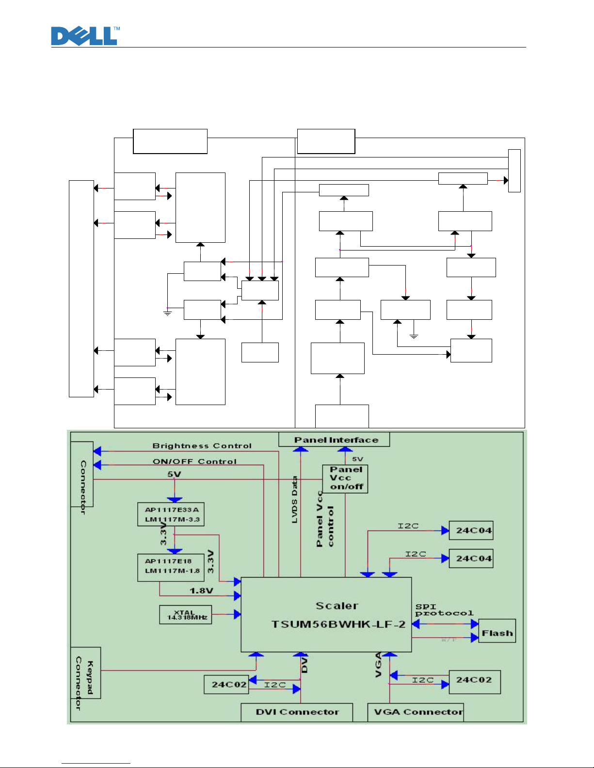
Chapter 3- CIRCUIT THEORY
Block Diagram
There are 2pcs PCBA in this monitor, one is power& inverter&Audio board which is a single layer
board, one is keypad which is OSD control.The system function block diagram as below
This PWA is included switching power supplier, inverter for CCFL and interface board.(fig.1)
OZ9937
MOSFET
MOSFET
Transformer1
Transformer2
Lamp1
Lamp2
Lamp3
Lamp4
AC Input
90V~264V
AC Line Filter
SG5841
PWM
Control
Rectifier&
Filter Circuit
Power
Transformer
Feedback
and OVP
Photocoupler
+16V DC output
+5V DC output
Brightness Control
ON/OFF Control
Feedback
Control
1
2
3
4
Power
MOSFET
To Panel CCFL
Snubber
&Schottky
Snubber
&Schottky
To IF Board
Fig.1
INVERTER POWER
Service Manual
6
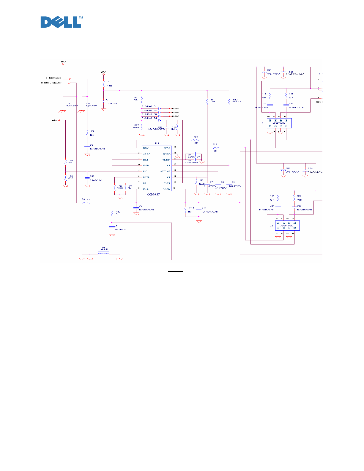
Electronic Circuit Theory
2.1 Inverter PWM circuit
2.1.1) Inverter Control circuit :( fig.2)
Fig.2
DC_5V through R1 and C1 will provide power for U1 on the pin2 (VDDA).
EN-ON/OFF voltage signal coming from scalar which is on IF BD will enable U1 to work. This
applies a level greater than approximately 2V to pin8 (ENA) enables the IC, A voltage less than 1V
will disable the IC. R3 is used to limit current.C3 and C40 is used to dump noise.
The soft-start function is provided by connecting C8 to pin12(SSTCMP), In the start-up mode,
current charges C8, its voltage controls the gradual increase in power to the transformer and
subsequently to the output load, this reduces in-rush current and provides reliable operation to the
CCFL.If no current is sensed approximately 2 seconds, U1 shuts off. Once the voltage at the pin4
(ISEN) reaches the lamp on threshold, the IC switches from the striking mode to the normal
operation mode and the PWM dimming control is activated.
DIM-ADJ duty cycle signal through R2 and C2 is on Pin 3(DIM), which adjusted will can
change the brightness of Panel.C41 is used to dump noise. Internal LPWM dimming control is
determined by R11 and C7 connected to LCT (pin11), analog dimming is implemented by providing
a DC voltage to PID (pin5).
The striking frequency is determined by R12 and C11 connected to Pin 13(CT) and R6
connected to RSTR (Pin6).The operating frequency is determined by R12 and C11 connected to
Pin 13(CT) and R7 connected to RT (pin7).
DRV1 and DRV2 of U1 are used to drive Q1 and Q2. DRV1 and DRV2 are controlled by
build-in PWM IC. Q1 and Q2 are switches which has two build-in IGBTs. The working principle of
circuit of T1 and T2.
Service Manual
7
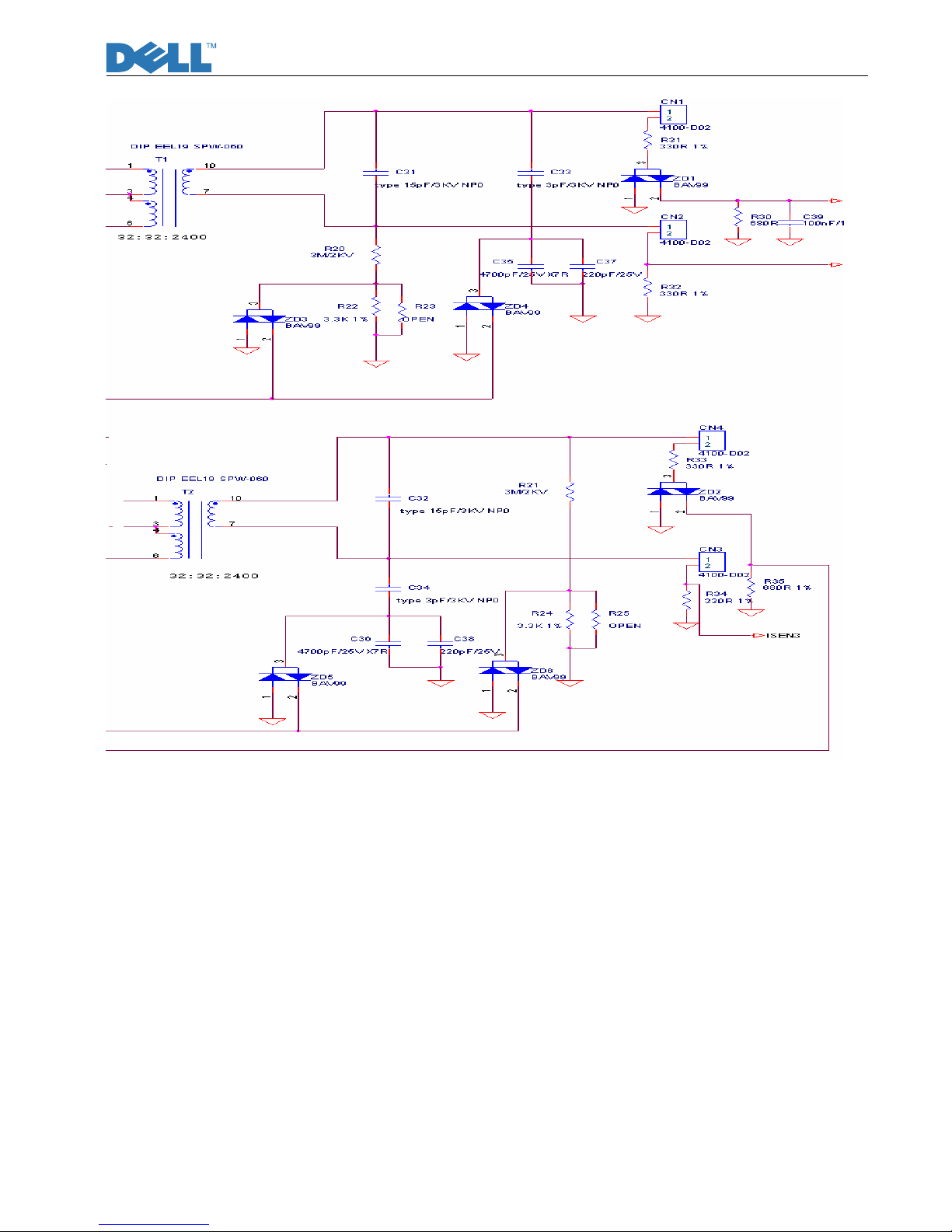
2.1.2) Output Circuit and Protection Circuit :( fig.3)
fig.3
The transformer (T1/T2) secondary winding leakage inductance and output capacitance
(C31/C32) forms a lower pass filter, which converts the square-wave driving signal into a sinusoidal
output voltage signal for CCFL.
The over-voltage protection feature is implemented by using an external capacitor divider
(C31/C32, C33/C34) or resistor divider (R20/R21, R22/R24) to sense the output voltage. The
divide-down voltage signal is sent to the IC Pin9 (VSEN), thus regulating the output voltage.
The voltage signal on negative pole of ZD1 sensed through R35 comes to Pin4 of U1 (ISEN).
The CCFL current detected at resistor R35 is converted to a voltage level and input to the ISEN
pin.C6 is used to dump noise. Once the CCFLs are ignited and current is sensed through resistor
R35, capacitor C6 performs the loop compensation function. The voltage at IC pin12 (SSTCMP)
controls the drive duty cycle of the power MOSFETs to regulate the CCFL current.
If a CCFL is removed, fails or damaged during normal operation, CCFL current is no longer
sensed and the voltage on ISEN pin drops. Once the voltage at the ISEN pin is less than the lamp”
on” threshold, the shutdown timer is activated. The IC maintains the output voltage for
approximately 2-3seconds and once the timer expires, the IC will shutdown. To restart the IC, either
toggle the SST_CMP pin or recycle the power on the VDDA pin.
Service Manual
8
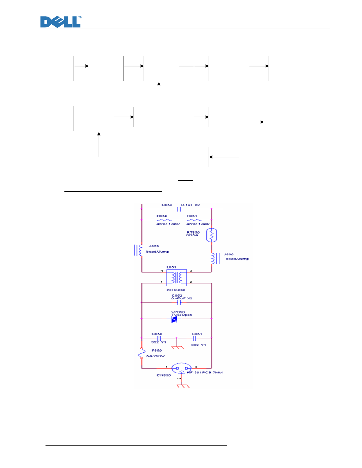
2.2 Power PWM circuit
2.2.1) Block diagram :( fig.4)
Fig.4
2.2.2) AC Input and EMI Filter :( fig.5)
fig.5
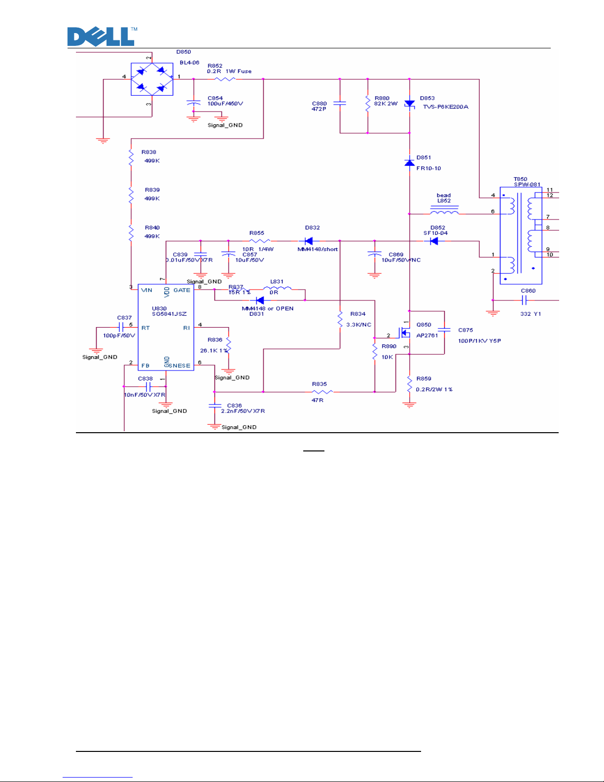
CN850 is a connector for connecting AC Power. F850 is a fuse to protect all the circuit AC.
Input voltage is from 90V to 264V. R850 and R851 are joined between two inputting main circuit
to prevent man from shock. L851 is used to clear up low frequency wave. C850 and C851 are
used to discharge the waves that L851 produced. High frequency waves are damped by C852
and C853.
2.2.3) High Voltage to Low Voltage Control Circuit :( fig.6)
EMI Filter
Rectifier and
filter
Isolation power
transformer
Rectifier and filter
Inverter circuit
PWM controller
Switching element
Feedback Isolation
Rectifier and filter
LDO regulator
Service Manual
9
fig.6
D850 is a rectifier in which there are 4 build-in diodes, inverting AC to DC.
C854 is used to smooth the wave from rectifier. R852 is a fuse resistor to protect the following
circuit when inrush current is too large. U850 is a highly integrated PWM controller. Typical
start-up current for U830 is only 8uA; R838, R839 and R840 are serial circuit to limit current flow.
When current flow through R838, R839 and R840 gets to Pin 3 of U830, with VDD hold-up
capacitor C857, U830 is enough for starting up.
When U830 begins to work, Pin8 (GATE) of U830 will output square wave to drive Q850, and
then the main current flow get to GND by passing through T850, Q850. Because of the change of
current flow, wires in the other side of T850 will induct current.At the same time, the current
inducted by wires which connected T850 Pin 1 and Pin 2, with components of D852, R855, C857
and C839, will be supplied to U830 for normal operating.
When the sense voltage across the sense resistor R859, reaches the threshold voltage around
0.85V, the output GATE drive will be turned off. Every time when the output of power supply is
shorted or over loaded, the FB voltage will increase, the build-in PWM output will then be turned off.
Both will prevent the power supply from being overheated under over loading condition. The PWM
duty cycle is determined by this current sense signal and VFB, the feedback voltage. When the
voltage on sense pin reaches Vcomp = (VFB-1.0)/3, a switch cycle will be terminated immediately.
Vcomp is internally clamped to a variable voltage around 0.85 V for output power limit.
When Q850 are turned off, the main current flow will be consumed through D851, C880, R880
and D853. This will prevent Q850 from being damaged under large current impulse and voltage
spike.
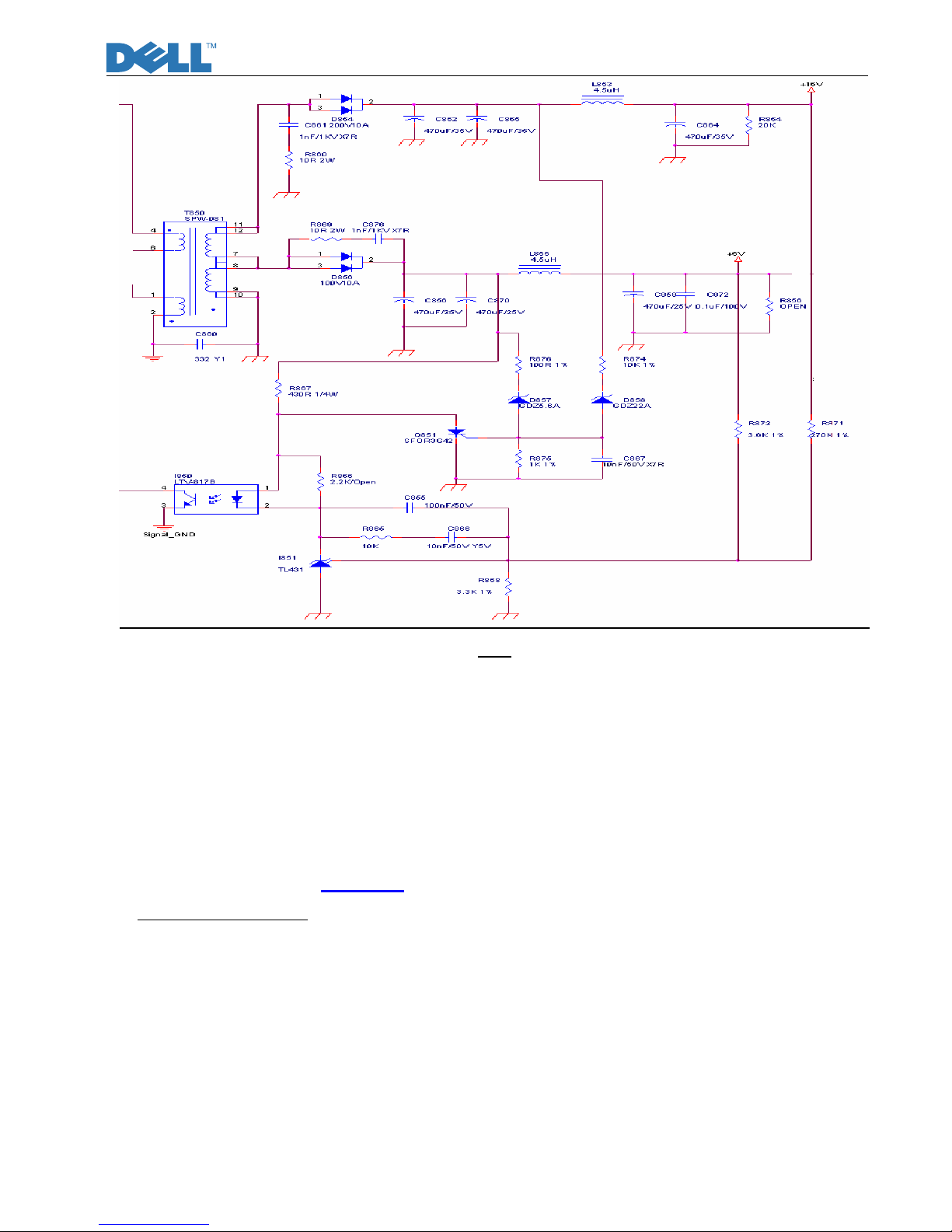
2.2.4) DC_16V and 5V Output Circuit and Feedback circuit :( fig.7)
Service Manual
10
fig.7
D854 is used to rectify the inducted current. R860 and C861 are used to store energy when
current is reversed. The parts including C862, C865, C864 and L853 are used to smooth the
current waves that are from D854, and then 16V voltage is supplied.
D856 is used to rectify the inducted current. R869 and C876 are used to store energy when
current is reversed. The parts including C856, C870, C859, C872 and L855 are used to smooth the
current waves that are from D856, and then 5V voltage is supplied.
16V and 5V supply voltage feed back to PWM controller U830 via R871, R872, R868 and
I850,I851.R865,C866 and C855 used to control respond time.
When 16V output or 5V output come out of SPEC , D857,D858 and Q851 will be operated, via
I850 ,U850 will be in Auto Restart mode until the matter is got rid of .
2.3 I/F Board Circuit (see the Attachment 2- Schematic)
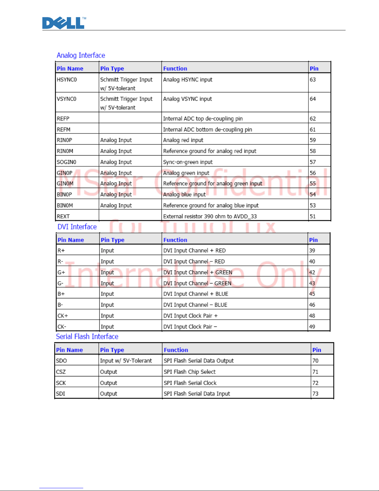
2.3.1 RGB CAPTURE
- Signal RED,GREEN,BLUE input through CN101 #1,#2,#3, Stop DC via C101, C102 and
C103, and then enter into U104 (TSUM56BWHK-LF) analog input PIN #59,#56,#54, and
then TSUM56BWHK-LF deals with signal internally. D101, D102, D103 are ESD protector to
prevent U104 from ESD.
- Signal DDC_SCL (series clock) inputs via CN101#15, and then passes through ZD104 for
ESD protection, goes into EDID EEPROM IC U102 #6.
- Signal DDC_SDA (series data) inputs via CN101#12, and then passes through ZD105 for
ESD protection, goes into EDID EEPROM IC U102 #5.
- Signal TTL vertical sync. (Vsync) inputs via CN101 #14, and then clamped by ZD103 Zener,
passes through R116, and then goes into IC U104 (TSUM56BWHK-LF) #64.
- Signal TTL horizontal sync. (Hsync) inputs via CN101 #13, and then clamped by ZD102
Zener, passes throughFB104 & R115, and then goes into IC U104 (TSUM56BWHK-LF) #63.
- CN101#5 is defined as cable detect pin, this detector realize via R113 and U104#26, and

Service Manual
11
ZD109 is ESD protector.
- U102 +3.3V is supplied by PC via CN101#9 with D104 and ZD101 for ESD protection, or
supplied by Monitor self via D104.
- U102 is an EEPROM IC which is memory and EDID data saved in it.
2.3.2 DVI CAPTURE
- Differential Signal input RX0+,RX0-,RX1+,RX1-,RX2+,RX2-,RXC+,RXC- through CN102
#18,#17,#10,#9,#2,#1,#23,#24 via R130,R131,R132,R133,R134,R135,R137,R138 enter
into U104 (TSUM56BWHK-LF) Digital input terminal #39,#40,#42,#43,#45,#46,#48,#49,
and then TSUM56BWHK-LF deals with signal internally. D108, D109, D110, D111, D112,
D113, D114, D115 are ESD protector to prevent U104 from ESD
- Signal DDC_SCL (series clock) inputs via CN102#6, and then passes through ZD106 Zener
for ESD protection, via R126, goes into EDID EEPROM IC U101 #6.
- Signal DDC_SDA (series data) inputs via CN102#7, and then passes through ZD107 Zener
for ESD protection, via R127, goes into EDID EEPROM IC U101 #5.
- CN102#15 is defined as cable detect pin, this detector realize passes through R125 ,go into
U104#27, and ZD110 is ESD protector.
- U101 +5V is supplied by PC via CN102#14 through D107, or supplied by Monitor self via
D107.
- U101 is an EEPROM IC which is memory and DVI input EDID data saved in it.
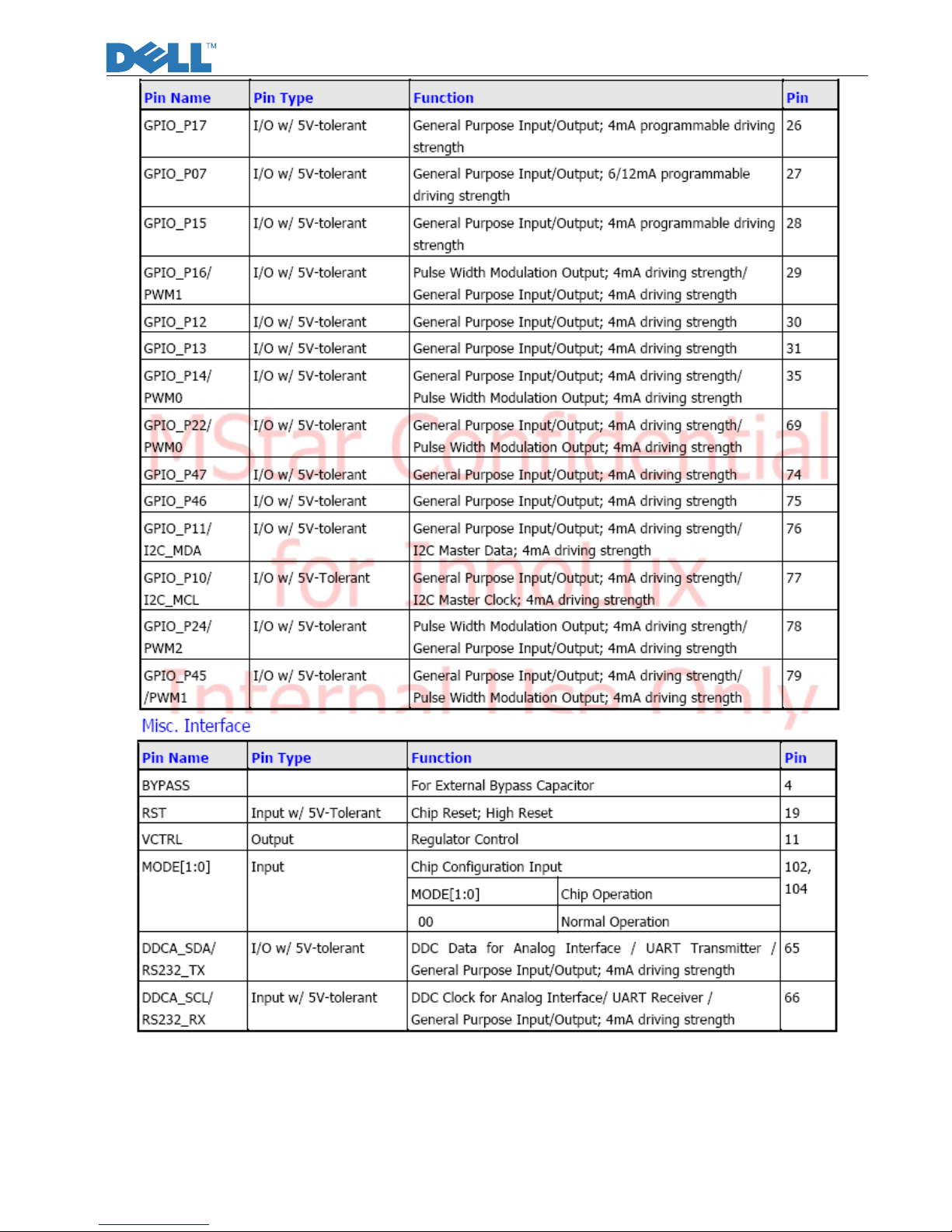
2.3.3 Buttons Control
- Button “Power” on front bezel connects to U104 (TSUM56BWHK-LF) #23 through CN104 #1,
U104 #23 is defined as power on/off.
- Button “Ï” on front bezel connects to U104 (TSUM56BWHK-LF) #24 through CN104 #2,
U104#24 Voltage is defined as “Plus”.
- Button “Д on front bezel connects to U104 (TSUM56BWHK-LF) #24 through CN104 #2,
U104 #24 Voltage is defined as “Minus”.
- Button “Menu” on front bezel connects to U104 (TSUM56BWHK-LF) #25 through CN104 #4,
U104 #25 Voltage is defined as “Menu”.
- Button “ENTER” on front bezel connects to U104 (TSUM56BWHK-LF) #25 through CN104
#4, U104 #25 Voltage is defined as “ENTER”.
- LED Indicator on Front Bezel
a. When press button “power”, U104 (TSUM56BWHK-LF) #31 be send in low Voltage, make
Q109#3 sends out high Voltage , and then to CN01#2 on keypad, LED white on.
b. When in “Suspend” mode, U104 (TSUM56BWHK-LF) #35 sends out a low Voltage, make
Q108#3 sends out high Voltage and then to CN01 #3 on keypad, LED Amber ON.
2.3.4 MATAR CHIP U104 (
TSUM56BWHK-LF)
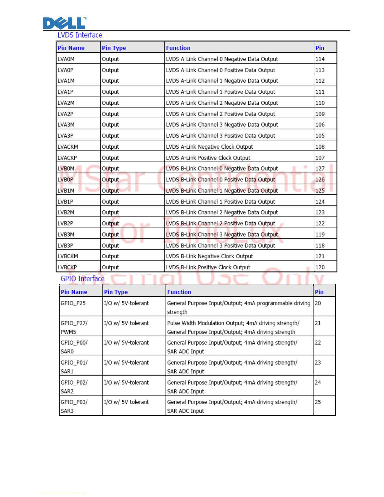
- U104 (TSUM56BWHK-LF ) #105~#114 output 8 bit even and #118~#127 output 8 bit odd
LVDS digital data to panel control circuit through CN106.
- U104 (TSUM56BWHK-LF ) #75 output PPWR ”H” potential to make Q106 conducted, and
then make Q103 conducted, +5V flow to CN106#1~#3 as Panel Vdd .
- U104 (TSUM56BWHK-LF) #20 output CCFL_ON/OFF ”L” potential to control Inverter on/off.
- U104 (TSUM56BWHK-LF) #21 outputs Brightness “PWM” signals to control CCFL
brightness.
- TCLK by Crystal 14.318MHz input to U104 (TSUM56BWHK-LF) #32.
- U104 (TSUM56BWHK-LF) #19 is RESET signals input pin
Please refer to TSUM56BWHK-LF Pin Assignments table in page
2.3.5 Regulator Circuit
- +5V is from switching mode power supply for panel
- +3.3V is generated from Regulator U103 which is supplied by+5V through C168 filtering,
C130 is 3.3V output filter ,the output 3.3V supplies toU104, U108,U107,U106,U105,U102,
U101.
Service Manual
12
- +1.8V is generated from Regulator U108 which is supplied byU103-3.3V through C143
filtering.The1.8V via FB105 supplies to U104.
3. FACTORY PRESET TIMING TABLE
Standard Resolution Horizontal Frequency
(KHz)
Vertical Frequency
(Hz)
640 x 480 31.469 59.940
640 x 480 37.500 75.000
800 x 600 37.879 60.317
800 x 600 46.875 75.000
1024 x 768 48.363 60.004
1024 x 768 60.023 75.029
1152x864 67.500 75.000
1280x1024 48.483 60.042
1280x1024 60.087 75.034
VESA
1440x900 55.935 59.887
IBM DOS 720 x 400 31.469 70.087
4. Power On/Off Sequency
Hardware power On/Off
When power cord plug into AC socket, Power provides 16V and DC_5V.
DC_5V is main voltage for panel and Regulator U103.
DC_3.3V is coming from Regulator U103, DC_3.3v is main voltage for U104. When DC_3.3V
input to U104 and U104 reset circuit active, U104 all registers will be set to default, that means
finish hardware power on.
When pull out power cord from AC socket,the system shut down instantly for no supply
Software power On/Off
- When press power key, U104 #23 receives low pulse, then (
TSUM56BWHK-LF) U104 will be
wake up and send control signals(at 20,75pin) to on CCFL and switch 5.0v to panel module,
at the same time,U104 make the VGA/DVI cable input signal source display normal on panel
if the VGA/DVI cable input signal is active
- If power ON, U104 #31 (LED_green) will send out low potential, and then LED white on.
- If power saveing, U104 #35 (LED_Amber) will send out low potential, and then LED Amber
on.
- If power ON or power saveing, when press power key, U104 #23 receives low pulse, then
U104 will be sleeping and turn off backlight, at the same time, the panel will lose +5V.
The Panel_Vcc, Backlight_En, CLK/DATA output to panel will follow the following sequency.
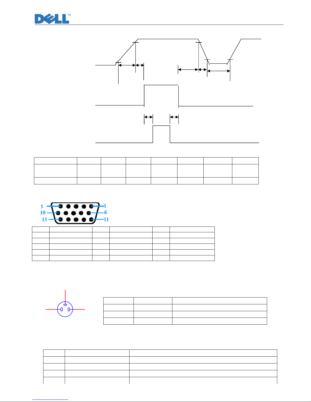
Service Manual
13
Power supply for panel+5V VDD
90% 90%
10%
0V 10%
T1 T2
T5 T6 T7
Signals Valid data
(Digital RGB, HS, VS, DE, CLOCK)
0V
T3 T4
Power supply for backlight
T1 (ms) T2 (ms) T3 (ms) T4 (ms) T5 (ms) T6 (ms) T7(ms)
SPEC
(Samsung)
0.3~10 0.0~50 >500 >200 0.0~50 NA >1000
SPEC (LPL) 0.5~10 0.01~50 >500 >200 0.01~50 NA >1000
5. D-SUB Connector Pin Assignment
6. AC input connector Pin Assignment
Pin Symbol Description
1 Line
AC Line(Vin=100 to 240 Vrms,50/60Hz)
2 GND GND
3 Neutral
AC Line(Vin=100 to 240 Vrms,50/60Hz)
7. Inner Connector Pin Assignment
7.1 CN106 (Connect M/B to Panel,)
Pin Symbol Description
1 Panel_Vcc Panel power supply (typ.5.0V)
2 Panel_Vcc Panel power supply (typ. 5.0V)
3 Panel_Vcc Panel power supply (typ. 5.0V)
4 NC
Pin Symbol Pin Symbol Pin Symbol
1 Red 6 Red_GND 11 GND
2 Green 7 Green_GND 12 DDC_SDA
3 Blue 8 Blue_GND 13 Hsync
4 GND 9 PC+5V 14 Vsync
5 Cable Detect 10 GND 15 DDC_SCL
CN850
1 3
2
Service Manual
14
5 NC
6 NC
7 GND_LVDS LVDS Ground
8 RXE3+ LVDS signal of even channel 3(-)
9 RXE3- LVDS signal of even channel 3(+)
10 RXEC+ LVDS signal of even channel clock (+)
11 RXEC- LVDS signal of even channel clock (-)
12 RXE2+ LVDS signal of even channel 2(+)
13 RXE2- LVDS signal of even channel 2(-)
14 GND_LVDS LVDS Ground
15 RXE1+ LVDS signal of even channel 1(+)
16 RXE1- LVDS signal of even channel 1(-)
17 GND_LVDS LVDS Ground
18 RXE0+ LVDS signal of odd channel 0(+)
19 RXE0- LVDS signal of odd channel 0(-)
20 RXO3+ LVDS signal of odd channel 3(+)
21 RXO3- LVDS signal of odd channel 3(-)
22 RXOC+ LVDS signal of even channel clock (+)
23 RXOC- LVDS signal of even channel clock (-)
24 GND_LVDS LVDS Ground
25 RXO2+ LVDS signal of even channel 2(+)
26 RXO2- LVDS signal of even channel 2(-)
27 RXO1+ LVDS signal of even channel 1(+)
28 RXO1- LVDS signal of even channel 1(-)
29 RXO0+ LVDS signal of odd channel 0(+)
30 RXO0- LVDS signal of odd channel 0(-)
7.2 CN1, CN2, CN3, CN4 (Connect to Panel Backlight,)
Pin Symbol Description
1 HV High voltage for lamp
2 LV Low voltage for lamp
7.3 CN104 (Connect to keypad, WAFER2*4P or compatible connector)
Pin Symbol Description
1 POWER OSD “POWER” control
2 PLUS/MINUS OSD “+/-” control and “AUTO/Brightness”adjustable hot
key
3 LED white LED white on/off control
4 MENU/ENTER OSD “MENU/ENTER” control
5 LED Amber LED amber on/off control
6 GND Ground
7 GND Ground
8 GND Ground
Service Manual
15
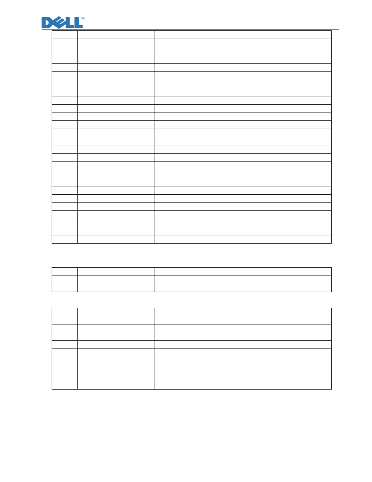
8. Key Parts Pin Assignments
8.1 U104(TSUM56BWHK-LF-2)
Service Manual
16
Service Manual
17
 Loading...