

Dell S1909WNf Service Manual

Service Manual
- 0 -
Service Manual
LCD Monitor S1909WNf

1
Service Manual Versions and Revision
No. Version Release Date Revision
1
1.0
2008/08/22
Initial Release
Copyright
Copyright 2007 InnoLux Display. Corp. Ltd
All Rights Reserved
This manual may not, in whole or in part, be copied, Photocopied, reproduced, translated, or converted to any
electronic or machine readable form without prior written permission of Foxconn Tech. Corp. Ltd.
Dell S1909WNf Service Manual

Service Manual
2
Table of Contents
CHAPTER 1- PRECAUTIONS & SAFETY NOTICES...........................................................................................................3
1. SAFETY PRECAUTIONS......................................................................................................................................3
2. PRODUCT SAFETY NOTICE................................................................................................................................3
3. SERVICE NOTES..................................................................................................................................................3
CHAPTER 2- SERVICE TOOLS & EQUIPMENT REQUIRED..............................................................................................4
CHAPTER 3- CIRCUIT THEORY...........................................................................................................................................5
1. BLOCK DIAGRAM......................................................................................................................................................5
2. ELECTRONIC CIRCUIT THEORY .................................................................................................................................7
3. FACTORY PRESET TIMING TABLE ................................................................................................................... 13
4. POWER ON/OFF SEQUENCY...................................................................................................................................13
5. D-SUB CONNECTOR PIN ASSIGNMENT ...................................................................................................................14
6. AC OUTLET PIN ASSIGNMENT.................................................................................................................................14
7. INNER CONNECTOR PIN ASSIGNMENT .....................................................................................................................14
8. KEY PARTS PIN ASSIGNMENTS................................................................................................................................16
CHAPTER 4- DISASSEMBLY & ASSEMBLY .....................................................................................................................21
1. EXPLODED DIAGRAM..............................................................................................................................................21
2. 1908WFPF DISASSEMBLY BLOCK ..........................................................................................................................22
3. ASSEMBLY BLOCK..................................................................................................................................................23
CHAPTER 5- TEST AND ADJUSTMENT............................................................................................................................24
1. FUNCTION KEY DEFINITIONS ...................................................................................................................................24
2. OSD CONTROL .....................................................................................................................................................24
3. FACTORY MODE INTRODUCTION..............................................................................................................................26
4. BURN-IN PATTERN ..................................................................................................................................................27
5. AUTO COLOR BALANCE (AUTOMATICALLY CALIBRATE CHIP ADC PARAMETER BY USING CHIP INTERNAL DAC.) ............27
6. UPLOAD FIRMWARE TO MCU VIA VGA CABLE..........................................................................................................26
7. AFTER REPAIR, TO ENSURE THE QUALITY YOU SHOULD DO THE FOLLOWING TEST AND ADJUSTMENT.............................27
CHAPTER 6- TROUBLE SHOOTING..................................................................................................................................30
1. COMMON ACKNOWLEDGE.......................................................................................................................................30
2. NO POWER LED OFF.............................................................................................................................................30
3. POWER NORMAL LED AMBER .................................................................................................................................31
4. BACKLIGHT CAN’T BE TURNED ON............................................................................................................................32
5. NO PICTURE BACKLIGHT ON..................................................................................................................................33
6. AT 32-GRAY SCALE PATTERN, COLOR LOST IN SOME SCALE .......................................................................................34
CHAPTER 7- RECOMMENDED PART LIST.......................................................................................................................35
ATT ACHMENT 1- BILL OF MATERIAL...............................................................................................................................37
ATT ACHMENT 2- SCHEMATIC...........................................................................................................................................47
ATT ACHMENT 3- PCB LAYOUT .........................................................................................................................................58

Service Manual
3
Chapter 1- PRECAUTIONS & SAFETY NOTICES
SAFETY PRECAUTIONS
This monitor is manufactured and tested on a ground principle that a user’s safety comes first.
However, improper used or installation may cause damage to the monitor as well as to the
user.
WARNINGS:
z This monitor should be operated only at the correct power sources indicated on the rating
label on the rear cover of the monitor. If you’re unsure the power supply in your residence,
consult your local dealer or Power Company.
z Use only the specified power cord that comes with this monitor.
z Do not try to repair the monitor by yourself, as it contains no user-serviceable parts. This
monitor should only be repaired by a qualified technician.
z Do not remove the monitor cabinet. There is high-voltage parts inside that may cause
electric shock to human bodies.
z Stop using the monitor if the cabinet is damaged. Have it checked by a service technician.
z Put your monitor only in a lean, cool, dry environment. If it gets wet, unplug the power
cable immediately and consult your closed dealer.
z Always unplug the monitor before cleaning it. Clean the cabinet with a clean, dry cloth.
Apply non-ammonia based cleaner onto the cloth, not directly onto the class screen.
z Do not place heavy objects on the monitor or power cord.
PRODUCT SAFETY NOTICE
Many electrical and mechanical parts in this chassis have special safety visual inspections
and the protection afforded by them cannot necessarily be obtained by using replacement
components rated for higher voltage, wattage, etc. Before replacing any of these components
read the parts list in this manual carefully. The use of substitute replacement parts, which do
not have the same safety characteristics as specified in the parts list, may create shock, fire,
or other hazards.
SERVICE NOTES
z When replacing parts on circuit boards, clamp the solder wires around terminals before
soldering.
z Keep wires away from high voltage, high temperature components and sharp edges.
z Keep wires in their original position so as to reduce interference.
z Adjustment of this product please refers to the user’ manual.
z Use Pb free solder wire for circuit board preparation.

Service Manual
4
Chapter 2- SERVICE TOOLS & EQUIPMENT REQUIRED
1. SIGNAL GENERATOR
2. MULTIMETER
3. SCREW DRIVER
4. OSCILLOSCOPE
5. Soldering IRON
6. SOLDER (Lead free, RoHS compliance)
7. Color Analyzer
8. Fox_VISP_Programmer
9. Fox_VEDID_Programmer
Service Manual
5
Chapter 3- CIRCUIT THEORY
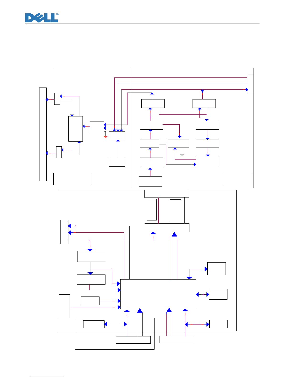
Block Diagram
There are 2pcs PCBA in this monitor, one is power& inverter board which is a single layer board,
one is interface board .The system function block diagram as below.This PWA is included
switching power supplier, inverter for CCFL and interface board.(fig.1)
Feedback
Control
1
Lamp1
To Panel CCFL
To IF Board
AC Line Filter
ON/OFF Control
Power
Transformer
Power
MOSFET
Photocoupler
Inverter
Transformer
MOSFET
+5V DC output
Snubber
&Schottky
2
INL836
AC Input
90V~264V
Brightness Control
Feedback
and OVP
Lamp2
PWM Control IC
LD7552B
Rectifier&
Filter
Circuit
Snubber
&Schottky
+12V DC output
24C02
Mstar TSUM1PEJ-LF-2
I2C
Flash
LVDS for 2
Channels
VGA Connector
5V
14.318MHz
LM1117MPX-1.8
DVI
3.3V
AP1117E33A/
I2C
Brightness Control
DVI Connector
VGA
LM1117MPX-3.3
24C04
Wire Harness
for 1 Channel
1.8V
One Connector
AP1117E18A/
XTAL
ON/OFF Control
SPI
Connector
24C02
Connector
5V
Scalar
Keypad
Panel Interface
I2C
DVI For Reserved
Fig.1
INVERTER POWER
Service Manual
6
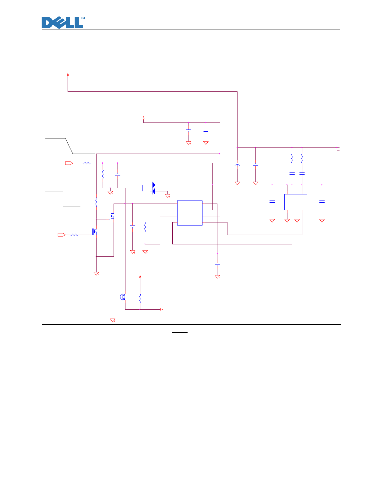
Electronic Circuit Theory
2.1 Inverter PWM circuit
2.1.1) Inverter Control circuit :( fig.2)
C5
1500pF/ 50V X7R
3.3V Light est
C27
1nF/50V
C22
1500pF/ 50V X7R
CCFL_ ON/O FF
C1
0.1/50V
Q2
RK7002
1
32
U1
INL836
8
7
6
2
3
1
54
ISEN
DIM
VDDA
RT
GNDA
SST_CMP
DRV1DRV2
OVP
R1
open
Q3
2N3904
E
B
C
R17
33R
C9
470uF/25V
C21
1500pF/ 50V X7R
C12
22nF/25V
C8
1nF/50V
ON/OF F5
R18
33R
C6
33nF/5 0V
+5V
Q1
RK7002
1
32
R5 10K
DIM5
Q4 AP9971GD
123
4
678
5
S1G1S2
G2
D2
D1D1D2
C23
2.2uF/16V
R22
47K
+12V
C2
0.1/50V
ZD7
open
2
3
1
Bright ness
3.3V On
R4
113K
0V of lightest
C25
open
0V Of f
+5V
R3 10K
R7
1M
Fig.2
DC_5V through C23 and C2 will provide power for U1 on the pin6.
EN-ON/OFF voltage signal coming from scalar which is on IF BD will enable U1 to work.
During start up, The voltage of SST_CMP is determined by Pin8(ISEN).When ON/OFF signal is off,
MOSFET Q1 will be closed, then upper resister R22 give high signal to Q2’ GATE pin, and make
IC’Pin1(SST_CMP) to GND, so IC will shut down. If giving a high signal to Q1, Q2 will be
closed .then Pin1 will be floating. Once the voltage at the ISEN pin reaches the lamp on threshold,
the IC switches from the striking mode to the normal operation mode and the PWM dimming
control is activated. At the same time, the voltage of Pin1 will change following the voltage of Pin 8.
R5 is limited current resister and C6 accomplishes the soft start function.
DIM-ADJ duty cycle signal through R3 and C5 is on Pin 7(DIM), which will adjust IC’ output
duty cycle, then changing the brightness of Panel
The striking and operating frequency is determined by the external resistor (R4) connected to Pin
2. The striking frequency is 1.3 times of normal frequency.
DRV1 and DRV2 of U1 are used to drive Q4. DRV1 and DRV2 are controlled by build-in PWM
IC. DRV1 is reverse with DRV2.Q4 is built in 2 N-chanel MOSFET. DRV1 and DRV2’PWM signal

Service Manual
7
drive Q4, this push and pull the energy in the transformer.
The voltage signal on negative pole of ZD4 sensed through R35 comes to Pin4 of U1, ISEN
(Lamp Current Detection & Control). The CCFL current is detected through R14and reaches a
regulated value. The CCFL current detected at resistor R14 is converted to a voltage level and
input to the ISEN pin.C12 is used to dump noise. Once the CCFL are ignited and current is sensed
through resistor R14 .capacitor C12 performs the loop compensation function. The voltage at IC
pin8 controls the drive duty cycle of the power MOSFET to regulate the CCFL current.
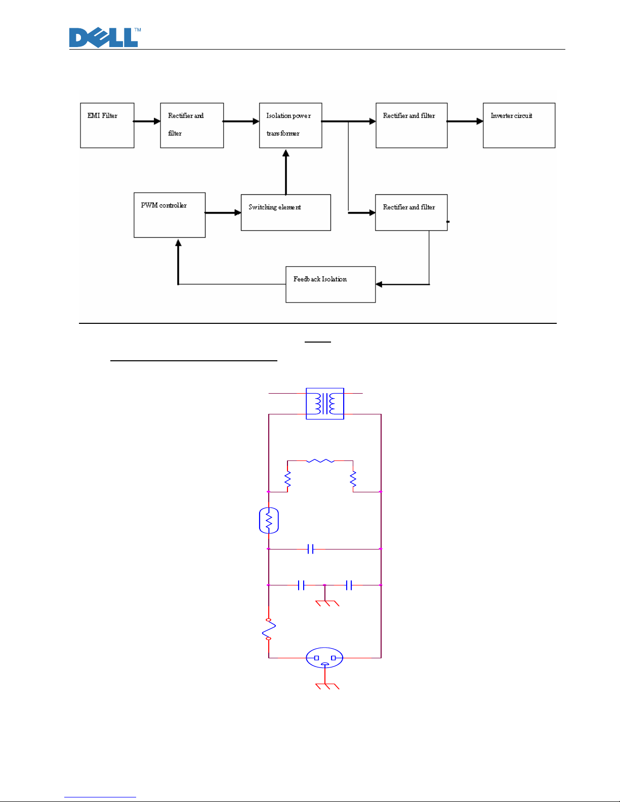
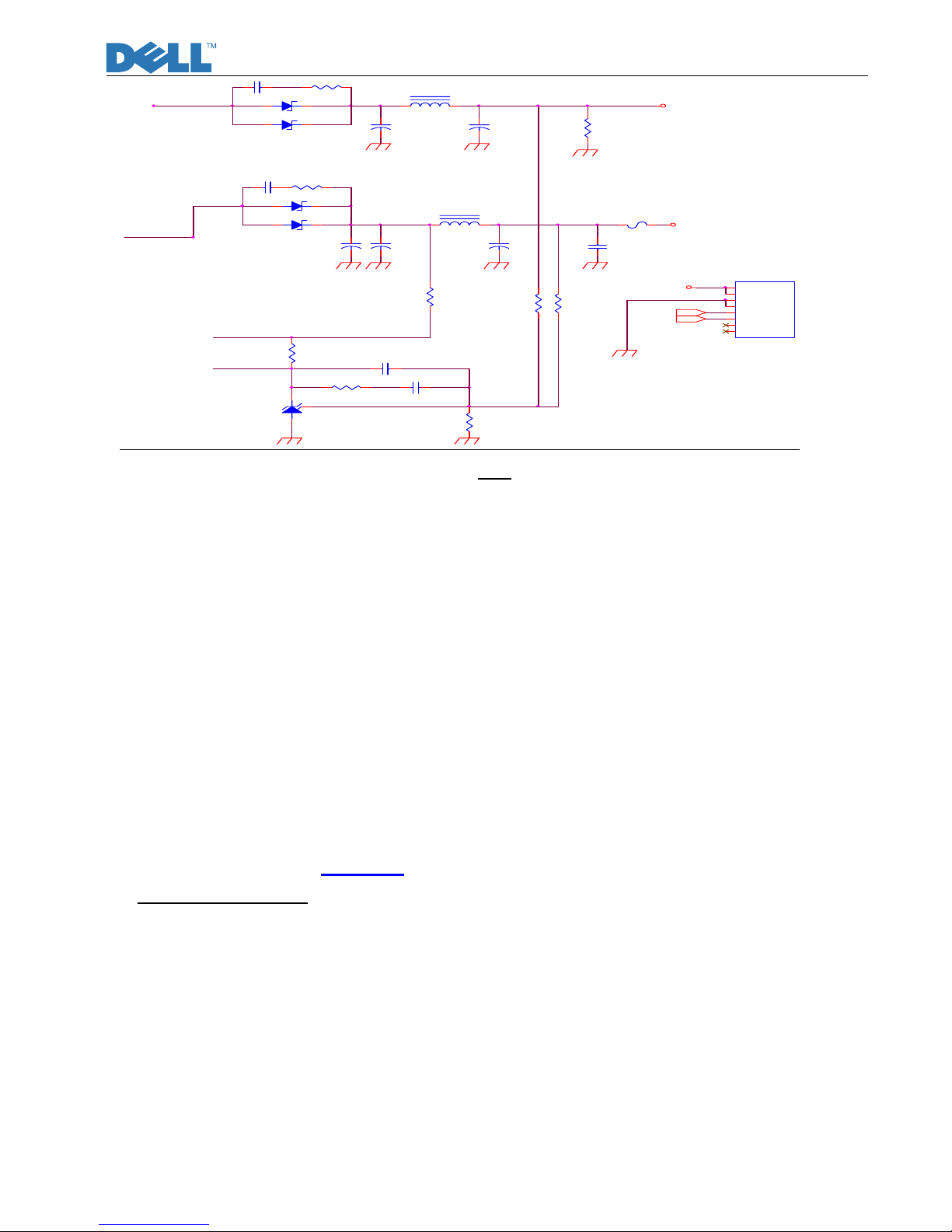
2.1.2) Output Circuit and Protection Circuit :( fig.3)
ZD6
BAV99
2
3
1
NC
CN4
1
2
4100-D02
CN2
1
2
T1
SPW-054
1
6
4
3
10
7
C17
3pF/3KV
C14
2700pF/50V X7R
ZD4
BAV99
2
3
1
+5V
C19
2700pF/50V X7R
OVP
C18
15pF/3KV
ZD5
BAV99
2
3
1
C24
NC/ 220pF/50V X7R
R14
390R 1%
4100-D02
CN1
1
2
C15
NC/ 220pF/50V X7R
NC
CN3
1
2
R6
1K
+5V
R2
1K
C13
3pF/3KV
OVP
fig.3
C9 and C2 is the filter capacitance.R17 and C21 as the snubber circuit will decrease the peak
voltage on Q4 drain pole witch have bad effort for MOSFET safety area.R18 and C22 have the
same effect with R17 and C21.C8 and C27 will deeply decrease the voltage on Q4 drain pole.
The transformer (T1) secondary winding leakage inductance and output capacitance(C18)
forms a lower pass filter, which converts the square-wave driving signal into a sinusoidal output
voltage signal for CCFL.
The over-voltage protection feature is implemented by using an external capacitor
devider(C13/C14,C17/C19) to sense the output voltage.The divide-down voltage signal is
transferred though ZD5 and ZD6,witch will rise the OVP voltage ,then this OVP signal though Q3
determine the voltage of SST_CMP ,thus regulating the output voltage.
If a CCFL is removed, fails or damaged during normal operation, CCFL current is no longer
sensed and the voltage on ISEN pin drops. Once the voltage at the ISEN pin is less than the lamp”
on” threshold, the shutdown timer is activated. The IC maintains the output voltage for
approximately 2-3seconds and once the timer expires, the IC will shutdown. To restart the IC, either
toggle the SST_CMP pin or recycle the power on the VDDA pin.
Service Manual
8
2.2 Power PWM circuit
2.2.1) Block diagram :( fig.4)
Fig.4
2.2.2) AC Input and EMI Filter :( fig.5)
L850
CHK-007
4 1
3 2
R852
499K
F850
3.15A 250V
CN850
HF-301PC B 7MM
1 3
2
R851 499K
C850
222 Y2
RT850
5R4A
C852
0.47uF X2
R850
499K
C851
222 Y2
fig.5
CN850 is a connector for connecting AC Power. F850 is a fuse to protect all the circuit AC.
Input voltage is from 90V to 264V. R850 ,R851 and R852 are joined between two inputting main
circuit to prevent man from shock. L850 is used to clear up low frequency wave. C850 and C851
are used to discharge the waves that L850 produced. High frequency waves are damped by
C852
Service Manual
9
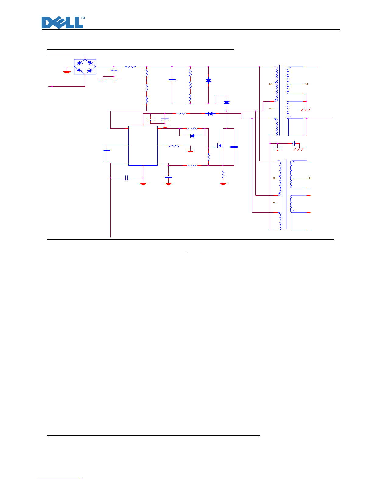
2.2.3) High Voltage to Low Voltage Control Circuit :( fig.6)
T850
SPW-119
3
2
1
5
6
8
9
10
11
12
7
4
C847
1nF/50V X7R
Signal_GND
R842
499K
R853
27K
D841
NC/1N 4148
R839 0. 2R/1W FUSE
C849
0.01uF/50V X7R
U850
LD7552B
1
45
2
83
7
6
GND
RTNC
COMP
OUTVCC
VCC
CS
C846
NC/47pF /50V X7R
Signal_GND
R843
499K
C854
68uF/450V
C875
472P
R859
0.75R/2W 1%
C860
332 Y1
R856
10R
C872
NC/100P/1KV Y5P
T851
NC
3
2
1
5
6
8
9
10
11
12
7
4
Signal_GND
R841
499K
D851
FR10-10
Signal_GND
R840
47R
D853
NC/P6KE170A
C848
1nF/50V X7R
R854
27K
R855
27K
R848
100K 1%
D852
SF10-04
Signal_GND
Q850
AP2762
2
13
R884
10K
-+
D850
BL4-06
3
1
2
4
R844 47R
C855
10uF/50V
Signal_GND
fig.6
D850 is a rectifier in which there are 4 build-in diodes, inverting AC to DC.
C854 is used to smooth the wave from rectifier. R839 is a fuse resistor to protect the following
circuit when inrush current is too large. U850 is a highly integrated PWM controller. Typical
start-up current for U850 is only 30 uA, R841, R842 and R843 are serial circuit to limit current
flow. When current flow through R838 and R839 gets to Pin 3 of U850, with VDD
hold-up capacitor C855, U850 is enough for starting up.
When U850 begins to work Pin8 of U850 will output square wave to drive Q850, and then the
main current flow get to GND bypassing through T850, Q850. Because of the change of current
flow, wires in the other side of T850 will induct current. At the same time, the current inducted by
wires which connected T850 Pin 1 and Pin 2, with components of D852, R855, C855 and C849,
will be supplied to U850 for normal operating.
When the sense voltage across the sense resistor R859, reaches the threshold voltage around
0.85V, the output GATE drive will be turned off. Every time when the output of power supply is
shorted or over loaded, the FB voltage will increase, the build-in PWM output will then be turned off.
Both will prevent the power supply from being overheated under over loading condition. The PWM
duty cycle is determined by this current sense signal and VFB, the feedback voltage. When the
voltage on sense pin reaches Vcomp = (VFB-1.0)/3, a switch cycle will be terminated immediately.
Vcomp is internally clamped to a variable voltage around 0. 85 V for output power limit.
When Q850 are turned off, the main current flow will be consumed through D851, C875 R853 ,
R854 and R855. This will prevent Q850 from being damaged under large current impulse and
voltage spike.
2.2.4) DC_12V and 5V Output Circuit and Feedback circuit :( fig.7)
Service Manual
10
DIM
C876
0.1uF/5 0V
ON/OF F
R858
NC/5K1
CN853
SIP-8P
2
1
3
4
6
5
7
8
+5V
+5V
GND
GND
DIM
ENA
Audio_detect
Audio_on/of f
F851
5A/125V
D855 SR520
R860
5K1
R887
20K
D854 SR520
C859
10nF/50V Y 5V
R857
270R
C862
1000pF/1KV X7R
D856 NC /SB5150
R871
270K
R868
3.3K
C873
1000pF/1KV X7R
C864
470uF/25V
C858
470uF/25V
L855
NC/CHK-XXX
+5V
R862
10R 2W
+5V
+12V
I851
TL431
C871 0. 1uF/50V
C857
470uF/25V
C856
470uF/25V
L854
CHK-XXX
D857 SB5150
C863
470uF/25V
R873
10R 2W
R872
3.6K
fig.7
D854 is used to rectify the inducted current. R862 and C862 are used to store energy when
current is reversed. The parts including C863, C864, and R887 are used to smooth the current
waves that are from D854 and D855, and then 12V voltage is supplied. We can see, there have two
parts C862 and R862 paralleling with D857,they have two functions ,One is used to damp the peak
voltage of D857, the other is used for EMI.
D857 is used to rectify the inducted current. R873 and C873 are used to store energy when
current is reversed. The parts including C856, C857, C858 , C876 and L854 are used to smooth
the current waves that are from D857, and then 5V voltage is supplied.C873 and R873 have the
same function with C862 and R862.
In order to limit the 5V and 12V over Spec, we need a sampling circuit to accomplish this
function. At first, use R871 ,R872 and R868 this divider circuit to sample 2.5V, and comparing it to a
reference voltage 2.5,so we will get a differential signal witch can control the current of I851(TL431).
R860,C859 and C871 is frequency compensating circuit witch be able to control feedback loop
speed rate,R857 is else able to accomplish this function, and its main task is getting current for
I851 and I850
2.3 I/F Board Circuit (see the Attachment 2- Schematic)
2.3.1 RGB CAPTURE
- Signal RED,GREEN,BLUE input through CN102 #1,#2,#3, Stop DC via C113, C114 and
C115, and then enter into U105 (TSUM1PEJ-LF-2) analog input PIN #28,#25,#23, and then
TSUM1PEJ-LF-2 deals with signal internally. D103, D104, D105 are ESD protector to
prevent U105 from ESD.
- Signal DDC_SCL (series clock) inputs via CN102#15, and then passes through ZD106 for
ESD protection, goes into EDID EEPROM IC U103 #6.
- Signal DDC_SDA (series data) inputs via CN102#12, and then passes through ZD103 for
ESD protection, goes into EDID EEPROM IC U103 #5.
- Signal TTL vertical sync. (Vsync) inputs via CN102 #14, and then clamped by ZD105 Zener,
passes through R134, and then goes into IC U105 (TSUM1PEJ-LF-2) #33.
- Signal TTL horizontal sync. (Hsync) inputs via CN102 #13, and then clamped by ZD104
Zener, passes throughFB101 & R133, and then goes into IC U105 (TSUM1PEJ-LF-2) #32.
- CN102#5 is defined as cable detect pin, this detector realize via R113 and U105#36, and
D102 is ESD protector.

Service Manual
11
- U103 +3.3V is supplied by PC via CN102#9 with D106 and ZD102 for ESD protection, or
supplied by Monitor self via D106.
- U103 is an EEPROM IC which is memory and EDID data saved in it.
2.3.2 DVI CAPTURE(NA)
- Differential Signal input RX0+,RX0-,RX1+,RX1-,RX2+,RX2-,RXC+,RXC- through CN102
#18,#17,#10,#9,#2,#1,#23,#24 via R130,R131,R132,R133,R134,R135,R137,R138 enter
into U104 (TSUM1PEJ-LF-2) Digital input terminal #39,#40,#42,#43,#45,#46,#48,#49, and
then TSUM56BWHK-LF deals with signal internally. D108, D109, D110, D111, D112, D113,
D114, D115 are ESD protector to prevent U104 from ESD
- Signal DDC_SCL (series clock) inputs via CN102#6, and then passes through ZD106 Zener
for ESD protection, via R126, goes into EDID EEPROM IC U101 #6.
- Signal DDC_SDA (series data) inputs via CN102#7, and then passes through ZD107 Zener
for ESD protection, via R127, goes into EDID EEPROM IC U101 #5.
- CN102#15 is defined as cable detect pin, this detector realize passes through R125 ,go into
U104#27, and ZD110 is ESD protector.
- U101 +5V is supplied by PC via CN102#14 through D107, or supplied by Monitor self via
D107.
- U101 is an EEPROM IC which is memory and DVI input EDID data saved in it.
2.3.3 Buttons Control
- Button “Power” on front bezel connects to U105 (TSUM1PEJ-LF-2) #4 through CN104 #1,
U105 #4 is defined as power on/off.
- Button “Ï” on front bezel connects to U105(TSUM1PEJ-LF-2) #24 through CN104 #2,
U105#120 Voltage is defined as “Plus”.
- Button “Д on front bezel connects to U104 (TSUM1PEJ-LF-2) #24 through CN104 #2, U105
#120 Voltage is defined as “Minus”.
- Button “Menu” on front bezel connects to U105 (TSUM1PEJ-LF-2) #121 through CN104 #4,
U105 #121 Voltage is defined as “Menu”.
- Button “ENTER” on front bezel connects to U105 (TSUM1PEJ-LF-2) #121 through CN104
#4, U104 #121 Voltage is defined as “ENTER”.
- LED Indicator on Front Bezel
a. When press button “power”, U105 (TSUM1PEJ-LF-2) #123 be send in low Voltage, make
Q107#3 sends out low Voltage , and then to CN01#2 on keypad, LED white on.
b. When in “Suspend” mode, U105 (TSUM1PEJ-LF-2) #124 sends out a low Voltage, make
Q108#3 sends out low Voltage and then to CN01 #3 on keypad, LED Amber ON.
2.3.4 MATAR CHIP U105 (
TSUM1PEJ-LF-2)
- U105 (TSUM1PEJ-LF-2 ) #86~#77 output 8 bit even and #100~#91 output 8 bit odd LVDS
digital data to panel control circuit through CN103.
- U105 (TSUM1PEJ-LF-2) #73 output PPWR ”H” potential to make Q104 conducted, and then
make Q101 conducted, +5V flow to CN103#1~#3 as Panel Vdd .
- U105 (TSUM1PEJ-LF-2) #109 output CCFL_ON/OFF ”L” potential to control Inverter on/off.
- U105 (TSUM1PEJ-LF-2) #125 outputs Brightness “PWM” signals to control CCFL
brightness.
- TCLK by Crystal 14.318MHz input to U105 (TSUM1PEJ-LF-2) #128.
- U105 (TSUM1PEJ-LF-2) #7is RESET signals input pin
Please refer to TSUM1PEJ-LF-2 Pin Assignments table in page
2.3.5 Regulator Circuit
- +5V is from switching mode power supply for panel
- +3.3V is generated from Regulator U101 which is supplied by+5V through C104 filtering,
C102 is 3.3V output filter ,the output 3.3V supplies to U102, U103,U105,U108.
- +1.8V is generated from Regulator U102 which is supplied byU101-3.3V through C106
filtering.The1.8V via FB105 supplies to U105.
Service Manual
12
3. FACTORY PRESET TIMING TABLE
Standard Resolution Horizontal Frequency
(KHz)
Vertical Frequency
(Hz)
640 x 480 31.469 59.940
640 x 480 37.500 75.000
800 x 600 37.879 60.317
800 x 600 46.875 75.000
1024 x 768 48.363 60.004
1024 x 768 60.023 75.029
1152x864 67.500 75.000
1280x1024 48.483 60.042
1280x1024 60.087 75.034
VESA
1366x768 55.935 59.887
IBM DOS 720 x 400 47.712 59.790
4. Power On/Off Sequency
Hardware power On/Off
When power cord plug into AC socket, Power provides 16V and DC_5V.
DC_5V is main voltage for panel and Regulator U103.
DC_3.3V is coming from Regulator U103, DC_3.3v is main voltage for U104. When DC_3.3V
input to U104 and U104 reset circuit active, U104 all registers will be set to default, that means
finish hardware power on.
When pull out power cord from AC socket,the system shut down instantly for no supply
Software power On/Off
- When press power key, U104 #23 receives low pulse, then (TSUM1PEJ-LF-2) U104 will be
wake up and send control signals(at 20,75pin) to on CCFL and switch 5.0v to panel module,
at the same time,U104 make the VGA/DVI cable input signal source display normal on panel
if the VGA/DVI cable input signal is active
- If power ON, U104 #31 (LED_green) will send out low potential, and then LED white on.
- If power saveing, U104 #35 (LED_Amber) will send out low potential, and then LED Amber
on.
- If power ON or power saveing, when press power key, U104 #23 receives low pulse, then
U104 will be sleeping and turn off backlight, at the same time, the panel will lose +5V.
The Panel_Vcc, Backlight_En, CLK/DATA output to panel will follow the following sequency.
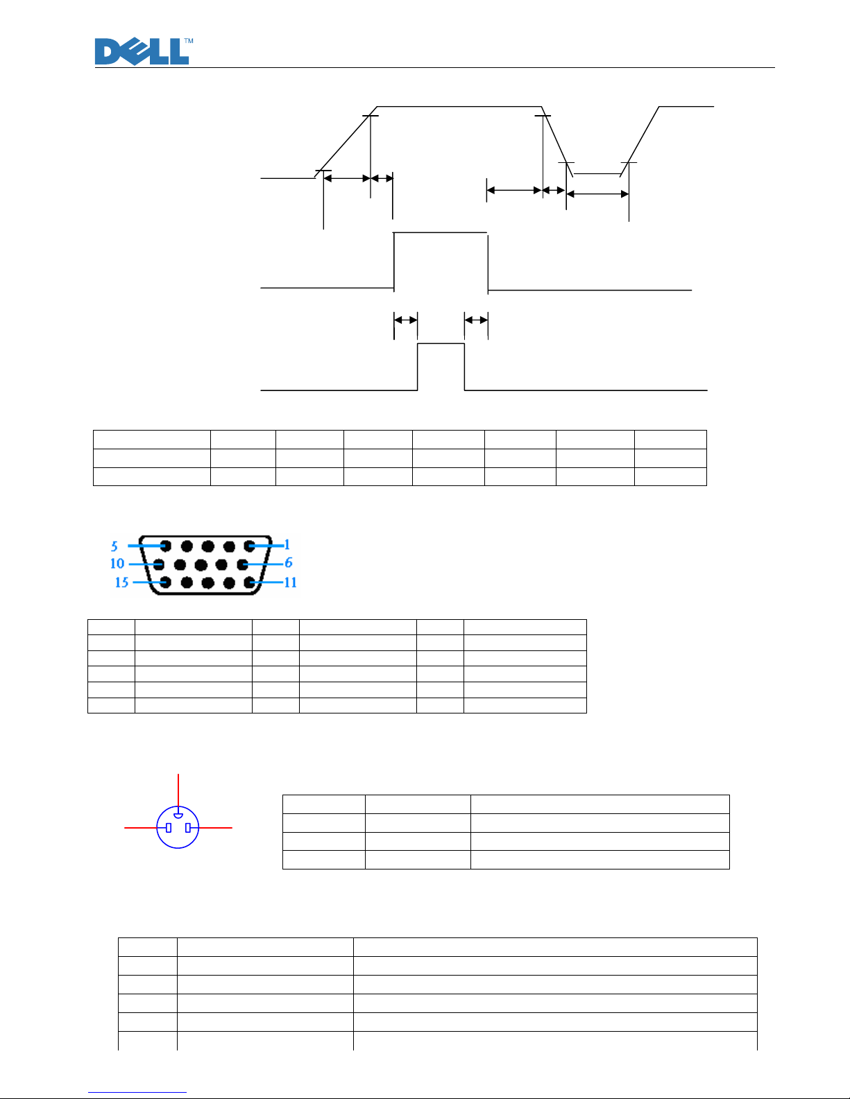
Service Manual
13
Power supply for panel+5V VDD
90% 90%
10%
0V 10%
T1 T2
T5 T6 T7
Signals Valid data
(Digital RGB, HS, VS, DE, CLOCK)
0V
T3 T4
Power supply for backlight
T1(ms) T2 (ms) T3 (ms) T4 (ms) T5 (ms) T6 (ms) T7(ms)
SPEC (AUO) 0.5~10 0.0~50 >200 >200 0.5~50 NA >1000
SPEC (LPL) 0.5~10 0.01~50 >500 >200 0.01~50 NA >1000
5. D-SUB Connector Pin Assignment
6. AC input connector Pin Assignment
Pin Symbol Description
1 Line
AC Line(Vin=100 to 240 Vrms,50/60Hz)
2 GND GND
3 Neutral
AC Line(Vin=100 to 240 Vrms,50/60Hz)
7. Inner Connector Pin Assignment
7.1 CN103 (Connect M/B to Panel,)
Pin Symbol Description
1 Panel_Vcc Panel power supply (typ.5.0V)
2 Panel_Vcc Panel power supply (typ. 5.0V)
3 Panel_Vcc Panel power supply (typ. 5.0V)
4 NC
5 NC
Pin Symbol Pin Symbol Pin Symbol
1 Red 6 Red_GND 11 GND
2 Green 7 Green_GND 12 DDC_SDA
3 Blue 8 Blue_GND 13 Hsync
4 GND 9 PC+5V 14 Vsync
5 Cable Detect 10 GND 15 DDC_SCL
CN850
1 3
2
Service Manual
14
6 NC
7 GND_LVDS LVDS Ground
8 RXE3+ LVDS signal of even channel 3(-)
9 RXE3- LVDS signal of even channel 3(+)
10 RXEC+ LVDS signal of even channel clock (+)
11 RXEC- LVDS signal of even channel clock (-)
12 RXE2+ LVDS signal of even channel 2(+)
13 RXE2- LVDS signal of even channel 2(-)
14 GND_LVDS LVDS Ground
15 RXE1+ LVDS signal of even channel 1(+)
16 RXE1- LVDS signal of even channel 1(-)
17 GND_LVDS LVDS Ground
18 RXE0+ LVDS signal of odd channel 0(+)
19 RXE0- LVDS signal of odd channel 0(-)
20 RXO3+ LVDS signal of odd channel 3(+)
21 RXO3- LVDS signal of odd channel 3(-)
22 RXOC+ LVDS signal of even channel clock (+)
23 RXOC- LVDS signal of even channel clock (-)
24 GND_LVDS LVDS Ground
25 RXO2+ LVDS signal of even channel 2(+)
26 RXO2- LVDS signal of even channel 2(-)
27 RXO1+ LVDS signal of even channel 1(+)
28 RXO1- LVDS signal of even channel 1(-)
29 RXO0+ LVDS signal of odd channel 0(+)
30 RXO0- LVDS signal of odd channel 0(-)
7.2 CN1, CN2 (Connect to Panel Backlight,)
Pin Symbol Description
1 HV High voltage for lamp
2 LV Low voltage for lamp
7.3 CN104 (Connect to keypad, WAFER2*4P or compatible connector)
Pin Symbol Description
1 POWER OSD “POWER” control
2 PLUS/MINUS OSD “+/-” control and “AUTO/Brightness”adjustable hot
key
3 LED white LED white on/off control
4 MENU/ENTER OSD “MENU/ENTER” control
5 LED Amber LED amber on/off control
6 GND Ground
7 GND Ground
8 GND Ground
 Loading...