

Page 1

Z
H
FRQQHFW
97&%
6RXWK%ULGJH
3,3&
3&,,QWHJUDWHG3HULSKHUDO&RQWUROOHU
3&&RPSOLDQW3&,WR,6$%ULGJH
ZLWK$&3,(QKDQFHG3RZHU0DQDJHPHQW60%XV
$3,&'LVWULEXWHG'0$6HULDO,543OXJDQG3OD\
8OWUD'0$0DVWHU0RGH3&,(,'(&RQWUROOHU
86%&RQWUROOHU.H\ERDUG&RQWUROOHUDQG57&
5HYLVLRQ
-XQH
9,$7(&+12/2*,(6,1&
Page 2
&RS\ULJKW1RWLFH
&RS\ULJKW 9,$ 7HFKQRORJLHV ,QFRUSRUDWHG 3ULQWHG LQ WKH 8QLWHG 6WDWHV $//5
1R SDUW RI WKLV GRFXPHQW PD\ EH UHSURGXFHG WUDQVPLWWHG WUDQVFULEHG VWRUHG LQ D UHWULHYDO V\VWHP RU WUDQVODWHG LQWR
DQ\ ODQJXDJH LQ DQ\ IRUP RU E\ DQ\ PHDQV HOHFWURQLF PHFKDQLFDO PDJQHWLF RSWLFDO FKHPLFDO PDQXDO RU RWKHUZLVH
ZLWKRXW WKH SULRU ZULWWHQ SHUPLVVLRQ RI 9,$ 7HFKQRORJLHV ,QFRUSRUDWHG
97&% PD\ RQO\ EH XVHG WR LGHQWLI\ D SURGXFW RI 9,$ 7HFKQRORJLHV ,QF
LV D UHJLVWHUHG WUDGHPDUN RI 9,$ 7HFKQRORJLHV ,QFRUSRUDWHG
70
36
&HOHURQ
:LQGRZV
3&,
$OO WUDGHPDUNV DUH WKH SURSHUWLHV RI WKHLU UHVSHFWLYH RZQHUV
LV D UHJLVWHUHG WUDGHPDUN RI ,QWHUQDWLRQDO %XVLQHVV 0DFKLQHV &RUS
70
3HQWLXP,,70 3HQWLXP,,,70 *7/70 $3,&70 DQG ,QWHO70DUH UHJLVWHUHG WUDGHPDUNV RI ,QWHO &RUS
70
70
LV D UHJLVWHUHG WUDGHPDUN RI WKH 3&, 6SHFLDO ,QWHUHVW *URXS
DQG 3OXJ DQG 3OD\70DUH UHJLVWHUHG WUDGHPDUNV RI 0LFURVRIW &RUS
,*+765(6(59('
'LVFODLPHU1RWLFH
1R OLFHQVH LV JUDQWHG LPSOLHG RU RWKHUZLVH XQGHU DQ\ SDWHQW RU SDWHQW ULJKWV RI 9,$ 7HFKQRORJLHV 9,$ 7HFKQRORJLHV
PDNHV QR ZDUUDQWLHV LPSOLHG RU RWKHUZLVH LQ UHJDUG WR WKLV GRFXPHQW DQG WR WKH SURGXFWV GHVFULEHG LQ WKLV GRFXPHQW
7KH LQIRUPDWLRQ SURYLGHG E\ WKLV GRFXPHQW LV EHOLHYHG WR EH DFFXUDWH DQG UHOLDEOH WR WKH SXEOLFDWLRQ GDWH RI WKLV
GRFXPHQW +RZHYHU 9,$ 7HFKQRORJLHV DVVXPHV QR UHVSRQVLELOLW\ IRU DQ\ HUURUV LQ WKLV GRFXPHQW )XUWKHUPRUH 9,$
7HFKQRORJLHV DVVXPHV QR UHVSRQVLELOLW\ IRU WKH XVH RU PLVXVH RI WKH LQIRUPDWLRQ LQ WKLV GRFXPHQW DQG IRU DQ\ SDWHQW
LQIULQJHPHQWV WKDW PD\ DULVH IURP WKH XVH RI WKLV GRFXPHQW 7KH LQIRUPDWLRQ DQG SURGXFW VSHFLILFDWLRQV ZLWKLQ WKLV
GRFXPHQW DUH VXEMHFW WR FKDQJH DW DQ\ WLPH ZLWKRXW QRWLFH DQG ZLWKRXW REOLJDWLRQ WR QRWLI\ DQ\ SHUVRQ RI VXFK FKDQJH
2IILFHV
86$ 2IILFH 7DLSHL 2IILFH
0LVVLRQ &RXUW
)UHPRQW &$ &KXQJ&KHQJ 5RDG +VLQ7LHQ
86$ 7DLSHL 7DLZDQ 52&
7HO 7HO
)D[ )D[
2QOLQH6HUYLFHV
+RPH 3DJH
)73 6HUYHU
%%6
http://www.via.com.tw
ftp.via.com.tw
¤RU
http://www.viatech.com
WK
)ORRU 1R
Page 3
7HFKQRORJLHV ,QF
&
:H&RQQHFW
RQQHFW
:H
R
EVISION HISTORY
Document Release Date Revision Initials
Revision 0.1 2/23/99 Initial release based on 82C596A Data Sheet revision 1.1
- Added UltraDMA-66 to feature bullets and overview
- Added integrated APIC (changed H18, K18, J17 pin descriptions)
- Added note to RTC CMOS Register Summary
- Added / changed function 0 Rx42[6], Rx48[7-4], Rx5B[3], Rx5C[7-4, 2],
Rx74[29-24, 8, 1], Rx87-89
- Added / changed function 3 Rx8, Rx4D[2-0], Rx54-55, Rx58-5B, Rx90-91,
RxD2-D6 (80-88 renumbered), PMU I/O Offset 0[11], 20[14, 7-1],
22[14, 7-1], 24[14, 7-1], 28[15-11], 2A[15-11], 2C[11-10], 38[2-1],
44[10-1], 4C[30-0]
Revision 0.2 3/9/99 Updated feature bullets, overview, and pin descriptions
Replaced IDE function 1 with registers from 686B to reflect UltraDMA-66
Added / changed PMU function 3 registers Rx42[7-6, 4], Rx58-5B, PMU I/O
Offset 0[8], 2C[2], 30[10-0], 34[10-0], 38[6, 4-3], 40 (removed)
Revision 0.3 6/17/99 Changed Function 0 Rx42[2-0], 43[5-4], 50 default, 55[3-0], 57[3-0], 58[3-0],
88[5], Function 1 RxD, 42-43, 45[3-2], 54[4-3], 70, 74-75, 78, 7C-7D,
Function 2 Rx41[7-3], Function 3 Rx4C-4F default value
VT82C596B
DH
DH
DH
Revision 0.3 June 17, 1999 -i- Revision History
Page 4

7HFKQRORJLHV ,QF
&
:H&RQQHFW
RQQHFW
:H
T
ABLE OF CONTENTS
VT82C596B
REVISION HISTORY........................................................................................................................................................................I
TABLE OF CONTENTS..................................................................................................................................................................II
LIST OF FIGURES..........................................................................................................................................................................IV
LIST OF TABLES ...........................................................................................................................................................................IV
OVERVIEW.......................................................................................................................................................................................3
PINOUTS............................................................................................................................................................................................4
REGISTERS.....................................................................................................................................................................................21
EGISTER OVERVIEW
R
ONFIGURATION SPACE
C
EGISTER DESCRIPTIONS
R
.................................................................................................................................................................21
I/O .......................................................................................................................................................28
............................................................................................................................................................29
Legacy I/O Ports...................................................................................................................................................................29
Keyboard Controller Registers.............................................................................................................................................................. 30
DMA Controller I/O Registers.............................................................................................................................................................. 32
Interrupt Controller Registers ............................................................................................................................................................... 33
Timer / Counter Registers..................................................................................................................................................................... 33
CMOS / RTC Registers......................................................................................................................................................................... 34
Function 0 Registers - PCI to ISA Bridge...........................................................................................................................35
PCI Configuration Space Header..........................................................................................................................................................35
ISA Bus Control.................................................................................................................................................................................... 36
Plug and Play Control........................................................................................................................................................................... 39
Distributed DMA / Serial IRQ Control................................................................................................................................................. 41
Miscellaneous / General Purpose I/O.................................................................................................................................................... 42
Function 1 Registers - Enhanced IDE Controller..............................................................................................................47
PCI Configuration Space Header..........................................................................................................................................................47
IDE-Controller-Specific Confiiguration Registers................................................................................................................................ 49
IDE I/O Registers.................................................................................................................................................................................. 54
Function 2 Registers - Universal Serial Bus Controller.....................................................................................................55
PCI Configuration Space Header..........................................................................................................................................................55
USB-Specific Configuration Registers.................................................................................................................................................. 56
USB I/O Registers................................................................................................................................................................................. 57
Function 3 Registers - Power Management and SMBus..................................................................................................58
PCI Configuration Space Header..........................................................................................................................................................58
Power Management-Specific PCI Configuration Registers .......................................................................... ........................................ 59
System Management Bus-Specific Configuration Registers................................................................................................................. 65
System Management Bus I/O-Space Registers...................................................................................................................................... 66
Power Management I/O-Space Registers..............................................................................................................................................70
FUNCTIONAL DESCRIPTIONS..................................................................................................................................................78
OWER MANAGEMENT
P
Power Management Subsystem Overview............................................................................................................................................ 78
Processor Bus States............................................................................................................................................................................. 78
System Suspend States and Power Plane Control................................................................................................................................. 79
General Purpose I/O Ports..................................................................................................................................................................... 79
Power Management Events................................................................................................................................................................... 80
System and Processor Resume Events.................................................................................................................................................. 80
Legacy Power Management Timers...................................................................................................................................................... 81
System Primary and Secondary Events................................................................................................................................................. 81
Peripheral Events.................................................................................................................................................................................. 81
................................................................................................................................................................78
ELECTRICAL SPECIFICATIONS...............................................................................................................................................82
Revision 0.3 June 17, 1999 -ii- Table of Contents
Page 5

7HFKQRORJLHV ,QF
&
:H&RQQHFW
RQQHFW
:H
BSOLUTE MAXIMUM RATINGS
A
HARACTERISTICS
DC C
IMING SPECIFICATIONS
AC T
................................................................................................................................................................82
.................................................................................................................................................82
......................................................................................................................................................83
VT82C596B
PACKAGE MECHANICAL SPECIFICATIONS........................................................................................................................90
Revision 0.3 June 17, 1999 -iii- Table of Contents
Page 6

7HFKQRORJLHV ,QF
&
:H&RQQHFW
RQQHFW
:H
L
IST OF FIGURES
FIGURE 1. PC SYSTEM CONFIGURATION USING THE VT82C596B.................................................................................3
FIGURE 2. VT82C596B BALL DIAGRAM (TOP VIEW)...........................................................................................................4
FIGURE 3. VT82C596B PIN LIST (NUMERICAL ORDER)......................................................................................................5
FIGURE 4. VT82C596B PIN LIST (ALPHABETICAL ORDER)............................................................................................... 6
FIGURE 5. STRAP OPTION CIRCUIT.......................................................................................................................................40
FIGURE 6. POWER MANAGEMENT SUBSYSTEM BLOCK DIAGRAM........................................................................... 78
FIGURE 8. ULTRADMA-33 IDE TIMING - DRIVE INITIATING DMA BURST FOR READ COMMAND....................85
FIGURE 9. ULTRADMA-33 IDE TIMING - DRIVE INITIATING BURST FOR WRITE COMMAND............................ 85
FIGURE 10. ULTRADMA-33 IDE TIMING - PAUSING A DMA BURST .............................................................................86
FIGURE 11. ULTRADMA-33 IDE TIMING - DRIVE TERMINATING DMA BURST DURING READ COMMAND....87
FIGURE 12. ULTRADMA-33 IDE TIMING - DRIVE TERMINATING DMA BURST DURING WRITE COMMAND .87
FIGURE 13. ULTRADMA-33 IDE TIMING - HOST TERMINATING DMA BURST DURING READ COMMAND......88
FIGURE 14. ULTRADMA-33 IDE TIMING - HOST TERMINATING DMA BURST DURING WRITE COMMAND...88
FIGURE 15. ULTRADMA-33 IDE TIMING - PIO CYCLE......................................................................................................89
FIGURE 16. MECHANICAL SPECIFICATIONS - 324-PIN BALL GRID ARRAY PACKAGE.........................................90
VT82C596B
L
IST OF TABLES
TABLE 1. PIN DESCRIPTIONS.....................................................................................................................................................7
TABLE 2. SYSTEM I/O MAP.......................................................................................................................................................21
TABLE 3. REGISTERS..................................................................................................................................................................21
TABLE 4. KEYBOARD CONTROLLER COMMAND CODES ..............................................................................................31
TABLE 5. CMOS REGISTER SUMMARY.................................................................................................................................34
TABLE 6. AC CHARACTERISTICS - PCI CYCLE TIMING..................................................................................................83
TABLE 7. AC CHARACTERISTICS - ULTRADMA-33 IDE BUS INTERFACE TIMING..................................................84
Revision 0.3 June 17, 1999 -iv- Table of Contents
Page 7

7HFKQRORJLHV ,QF
&
:H&RQQHFW
RQQHFW
:H
VT82C596B
VT82C596B PIPC
PCI I
WITH
ACPI, E
APIC, D
U
LTRA
DMA-33/66 M
USB C
Inter-operable with VIA and other Host-to-PCI Bridges
•
−
Combine with VT82C598 (Apollo MVP3) for a complete 66 / 75 / 83 / 100MHz Socket-7 PCI / AGP / ISA system
−
Combine with VT82C693 (Apollo ProPlus) for a complete 66 / 100 MHz Socket-370 or Slot-1 PCI / ISA system
−
Combine with VT82C693A (Apollo Pro133) for a complete 66 / 100 / 133 MHz Skt-370 or Slot-1 PCI / ISA system
PC98 Compliant PCI to ISA Bridge
•
−
Integrated ISA Bus Controller with integrated DMA, timer, and interrupt controller
−
Integrated Keyboard Controller with PS2 mouse support
−
Integrated DS12885-style Real Time Clock with extended 256 byte CMOS RAM and Day/Month Alarm for ACPI
−
Integrated USB Controller with root hub and two function ports
−
Integrated UltraDMA-33/66 master mode EIDE controller with enhanced PCI bus commands
−
PCI-2.1 compliant with delay transaction
−
Eight double-word line buffer between PCI and ISA bus
−
One-level PCI to ISA post-write buffer
−
Supports type F DMA transfers
−
Distributed DMA support for ISA legacy DMA across the PCI bus
−
Sideband signal support for PC/PCI and serial interrupt for docking and non-docking applications
−
Serial Interrupt input
−
Fast reset and Gate A20 operation
−
Edge trigger or level-sensitive interrupts
−
Flash EPROM, 2Mb EPROM and combined BIOS support
−
Supports positive and subtractive decoding
NTEGRATED PERIPHERAL CONTROLLER
PC98 C
OMPLIANT
PCI-TO-ISA B
NHANCED POWER MANAGEMENT
ISTRIBUTED
DMA, S
ERIAL
ASTER MODE
ONTROLLER
, K
EYBOARD CONTROLLER, AND
RIDGE
IRQ, P
LUG AND PLAY
PCI-EIDE C
, SMBUS,
,
ONTROLLER
RTC
,
Universal Serial Bus Controller
•
−
USB v.1.1 and Intel Universal HCI v.1.1 compatible
−
Eighteen level (doublewords) data FIFO with full scatter / gather capabilities
−
Root hub and two function ports
−
Integrated physical layer transceivers with over-current detection status on USB inputs
−
Legacy keyboard and PS/2 mouse support
Advanced Programmable Interrupt Controller (APIC)
•
−
Integrated on-chip
−
Control pins provided for support of optional external APIC
−
Used to extend system interrupt capability
−
PC98 compliant
Revision 0.3 June 17, 1999 -1- Features
Page 8

7HFKQRORJLHV ,QF
&
:H&RQQHFW
RQQHFW
:H
UltraDMA-33/66 Master Mode PCI EIDE Controller
•
−
Dual channel master mode PCI supporting four Enhanced IDE devices
−
Transfer rate up to 22MB/sec to cover PIO mode 4, multi-word DMA mode 2 drives, and beyond
−
Extension to UltraDMA-33 interface for transfer rates to 33MB/sec
−
Extension to UltraDMA-66 interface for transfer rates to 66MB/sec
−
Thirty-two levels (doublewords) of prefetch and write buffers
−
Dual DMA engine for concurrent dual channe l operation
−
Bus master programming interface for SFF-8038i rev.1.0 and Windows-95 compliant
−
Full scatter gather capability
−
Support ATAPI compliant devices including DVD devices
−
Support PCI native and ATA compatibility modes
−
Complete software driver support
−
Supports glue-less “Swap-Bay” option with full electrical isolation
System Management Bus Interface
•
−
Host interface for processor communications
−
Slave interface for external SMBus masters
Sophisticated PC98-Compatible Mobile Power Management
•
−
Supports both ACPI (Advanced Configuration and Power Interface) and legacy (APM) power management
−
ACPI v1.0 Compliant
−
APM v1.2 Complia nt
−
CPU clock throttling and clock stop control for complete ACPI C0 to C3 state support
−
PCI bus clock run a nd PCI/CPU clock gene rator stop control
−
Supports multiple system suspend types: power-on suspends with flexible CPU/PCI bus reset options,
suspend to DRAM, and suspend to disk (soft-off), all with hardware automatic wake-up
−
Multiple suspend power plane controls and suspend status indicato rs
−
One idle timer, one peripheral timer and one general purpose timer, plus 24/32-bit ACPI compliant timer
−
Normal, doze, sleep, suspend and conserve modes
−
Global and local device power control
−
System event monitoring with two event classes
−
Primary and secondary interrupt differentiation for individual channels
−
Dedicated input pins for power and sleep buttons, external modem ring indicator, and notebook lid open/close for
system wake-up
−
Up to 22 general purpose input ports and 31 output ports
−
Multiple internal and external SMI sources for flexible power management models
−
Two programmable chip selects and one microcontroller chip select
−
Enhanced integrated real time clock (RTC) with date alarm, month alarm, and century field
−
Thermal alarm support
−
Cache SRAM power-down control
−
Hot docking support
−
I/O pad leakage control
VT82C596B
Plug and Play Controller
•
−
PCI interrupts steerable to any interrupt channel
−
Dual interrupt and DMA signal steering for on-board plug and play devices
−
Microsoft Windows 95
Built-in NAND-tree pin scan test capability
•
0.5u, 3.3V, low power CMOS process
•
Single chip 324 pin BGA
•
Revision 0.3 June 17, 1999 -2- Features
TM
and plug and play BIOS compliant
Page 9
7HFKQRORJLHV ,QF
&
:H&RQQHFW
RQQHFW
:H
O
VERVIEW
VT82C596B
The VT82C596B south bridge is a high integration, high performance, power-efficient, and high compatibility device that supports
PCI / ISA bus bridge functionality to make a complete Microsoft PC98-compliant system. In addition to complete ISA extension
bus functionality, the VT82C596B includes standard intelligent peripheral controllers:
a) Master mode enhanced IDE controller with dual channel DMA engine and interlaced dual channel commands. Dedicated
FIFO coupled with scatter and gather master mode operation allows high performance transfers between PCI and IDE
devices. In addition to standard PIO and DMA mode operation, the VT82C596B also supports the UltraDMA-33 standard to
allow reliable data transfer rate s up to 33 MB /se c thro ughp ut and the Ultra DMA-66 stand ar d fo r 6 6M B/ sec d ata transfer . T he
IDE controller is SFF-8038i v1.0 and Microsoft Windows-95 / 98 / NT compliant.
b) Universal Serial Bus controller that is USB v1.1 and Universal HCI v1.1 compliant. The VT82C596B includes the root hub
with two function ports with integrated physical layer transceivers. The USB controller allows hot plug and play and
isochronous peripherals to be inserted into the system with universal driver support. The controller also implements legacy
keyboard and mouse support so that legacy software can run transparently in a non-USB-aware operating system
environment.
c) Keyboard controller with PS2 mouse support.
d) Real Time Clock with 256 byte extended CMOS. In addition to the standard ISA RTC functionality, the integrated RTC also
includes the date alarm, century field, and other enhancements for compatibility with the ACPI standard.
e) Notebook-class power management functionality compliant with ACPI and legacy APM requirements. Multiple sleep states
(power-on suspend, suspend-to-DRAM, and suspend-to-Disk) are supported with hardware automatic wake-up. Additional
functionality includes event monitoring, CPU clock throttling and stop (Intel processor p rotoco l), PCI b us clock stop control,
modular power, clock and leakage control, hardware-based and software-based event handling, general purpose I/O, chip
select and external SMI.
f) Full System Management Bus (SMBus) interface.
g) Distributed DMA capability for support of ISA legacy DMA over the PCI bus. PC/PCI and Serial IRQ mechanisms are also
supported for docking and non-docking applications.
h) Plug and Play controller that allows complete steerability of all PCI interrupts to any interrupt channel. Three additional
steerable interrupt channels are provided to allow plug and play and reconfigurability of on-board perip herals for Windows
95 compliance.
i) Integrated APIC (see the Win98 Hardware Design Guide)
The VT82C596B also enhances the functionality of the standard ISA peripherals. The integrated interrupt controller supports both
edge and level triggered interrupts channel by channel. The integrated DMA controller supports type F DMA in addition to
standard ISA DMA modes. Compliant with the PCI-2.1 specification, the VT82C596B supports delayed transactions so that
slower ISA peripherals do not block the traffic of the PCI bus. Special circuitry is built in to allow concurrent operation without
causing dead lock even in a PCI-to-PCI bridge environment. The chip also includes eight levels (doublewords) of line buffers from
the PCI bus to the ISA bus to further enhance overall system performance.
CPU / Cache
Sideband Signals:
Init / CPUreset
IRQ / NMI
SMI / StopClk
FERR / IGNNE
Boot ROM
CA
CD
RTC
Crystal
North Bridge
VT82C596B
324 BGA
MA/Command
MD
PCI
I2C (Module ID)
USB
KBC
IDE
GPIO, Power Control, Reset
ISA
System Memory
Expansion
Cards
Figure 1. PC System Configuration Using the VT82C596B
Revision 0.3 June 17, 1999 -3- Overview
Page 10
7HFKQRORJLHV ,QF
&
:H&RQQHFW
RQQHFW
:H
P
INOUTS
VT82C596B
Figure 2. VT82C596B Ball Diagram (Top View)
Key1234567891011121314151617181920
PCI
A
RST#AD27IDSELAD19
AD31AD26AD23AD18I
B
AD30AD25AD22AD17T
C
AD28CBE3#AD20CBE
D
AD29AD24AD21AD16DEV
E
USB-
F
G
H
J
K
L
M
N
P
R
T
U
V
W
Y
GPO28GPO29
P1+
PIRQD#USB-
GPI18USB
USB
OC0#
KBCS#
/MSDT
RTC-
ALE
REQA#RTC
GNTA#REQB#NC /
A20G/
MSCK
CPU
STP#
SD6SD
IRQ
9
SD
7
RST
DRV
IO
CHK#
SCI#
GPI21GPO0GPO
P0+
USB
P1-
P0-
USB
GPI14NC /
OC1#
ROM
GPI16GPI
CS#
GPI13USB
CLK
CS#XDIR#XOE#
KBCKMCCS#
GNTB#REQC#GNTC#PIRQ
PCI
PIRQA#PIRQ
STP#
IOCH
RDY
3
SMEMW#SA18DRQ3DRQ1SA11IRQ5SA
SD
2
DRQ
SD
2
SD4SD
SD
ZWS# AEN IOR#
5
0
1
FRA
SERR#
ME#
RDY#
RDY#
STOP#
2#
SEL#AD15
GPO
VCC VCC VCC VCC
30
27
GPI19GPI
20
GND
KEYL
USB
VCC
17
USB
PCS0#GPI
15
NC /
KBDT
PCS
1#
C#
NC VCC VCC VCC
B#
IOW#
SMEMR#SA17DACK
SA
16
SA19DACK3#SA14SA12IRQ6SA
AD13AD9AD5AD1PCI
AD12AD8AD4AD0PCI
PAR
CBE1#AD11CBE0#AD3PCK
AD14AD10AD6AD
GND
VCC
VCC
B
CLKSA9
RFSH#
1#
SA15SA13IRQ7SA8DACK2#SA3MCS
2
AD
VCC
7
GND GND GND GND VREF
GND GND GND GND
GND GND GND GND
GND GND GND GND
IRQ3SA4SA1LA23IRQ12LA18DACK
6
7
SA10IRQ4SA5SA2S
RQB#PGNT#SDD6SDD4SDD13SDDRQ
RQC#PREQ#SDD9SDD11SDD1SDIOW#SDA1SDCS1#PDD9PDD6
RUN#
RQA#
BALE
PCI
RQD#SDD7SDD5SDD3SDD14SDIOR#SDA0SDCS3#PDD10PDD5
GND
P
CLKSDD8SDD10SDD2SDD15SDRDYPDD12PDD3PDD11PDD4
PCI
VCC VCC GND
SA0IRQ10LA20DACK0#MEMW#DRQ6DRQ7SUSC#BAT
TC OSC
IOCS
16#LA21
BHE#
16#LA22
SD
D12SDD0
VCC
5#
IRQ14MEMR#DACK
IRQ11LA19DRQ
0
IRQ15LA17DRQ
DACK#
VCC
PD
IOW#PDIOR#PDDRQPDD15PDD0
PDA0PDA2PDA1PD
PD
CS3#PDCS1#
AAK#/
ZZ SPKR
V
BAT
NC
VCC
ALRT#
SUS
LID
VCC
SUS
SD9
6#
DACK
SD
8
5
SDA2PDD8PD
SD
PD
D14PDD1PDD13PDD2
DACK#
RDY
ACS#/
APD0THRM#
STP
APD1
CLK#
ARQ#/
WSC#
IGN
INIT INTR NMI
NE#
RSM
PWRGDCPU
RST#
SMB
NC
SUS
RI#
CLK
CFG1CFG2SMB
SUS
SUS
ST1#
ST2#
SD
TEST#
11
SD13SD
7#
SD10SD12SD
IRQ0
OUT
SER
IRQ
FERR# SLP#
RST
RTCX1RC
GPI
SMI#
1
RTC
CLK
GPO8SMB
DATA
PWR
LOW#
BTN#
SUSB#EXT
SMI#
SUS
15
14
D7
PD
IRQ
1
A20
M#
IN#
X2
A#
IRQ
8#
Note: Some of the pins above have alternate functions and alternate names. The table above contains only one name, but the pin lists and pin descriptions contain
all names.
Revision 0.3 June 17, 1999 -4- Pinouts
Page 11
7HFKQRORJLHV ,QF
&
Q
Q
:H&RQQHFW
RQQHFW
:H
VT82C596B
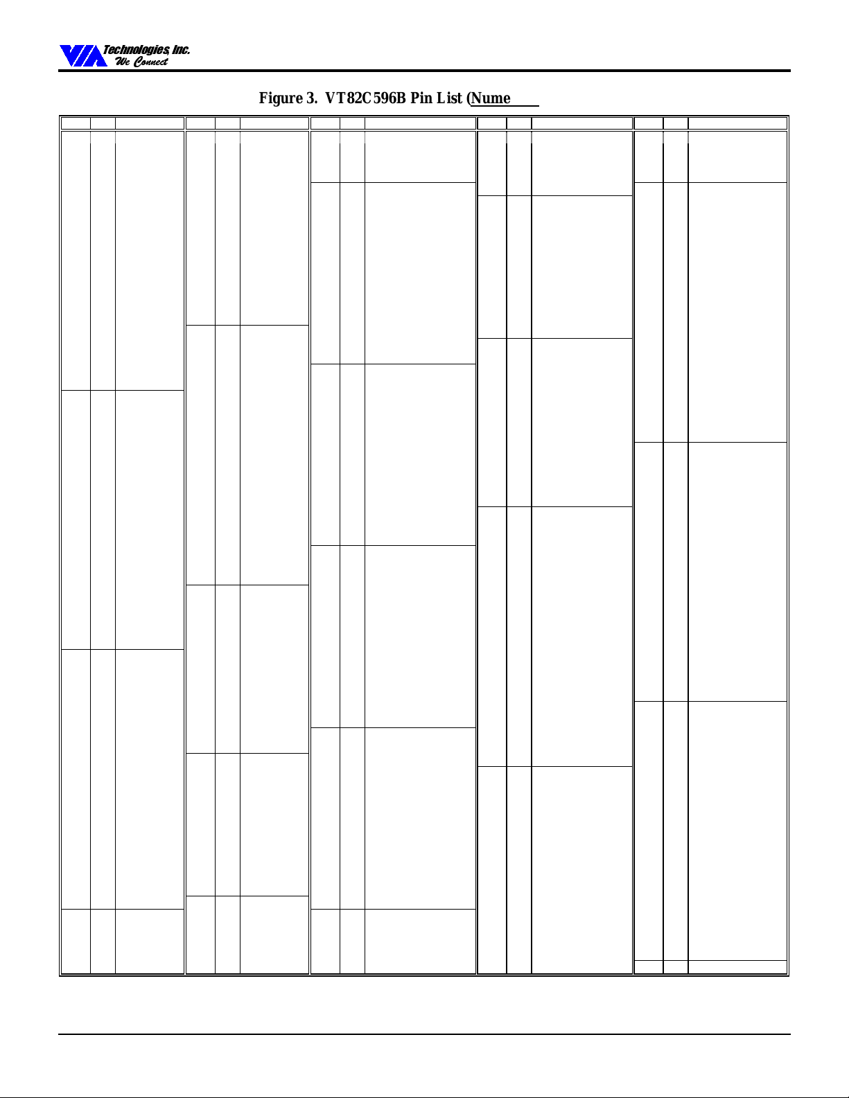
Figure 3. VT82C596B Pin List (Numerical Order)
Pin Pin
A01 O PCIRST# D06 IO AD14 H17 O PDCS1#
A02 IO AD27 D07 IO AD10 H18 O APICCS#/D0/GPO13 N17 I SMBALRT# / GPI11 U18 O SUSC# / GPO16
A03 I IDSEL D08 IO AD6 H19 I THRM# / GPI8 N18 - NC U19 I BATLOW# / GPI9
A04 IO AD19 D09 IO AD2 H20 O IRQ0OUT / GPO14 N19 I RTCX1 U20 I PWRBTN#
A05 IO FRAME#
A06 I SERR# D11 I PCLK J02 I USBOC1# P01 IO A20GATE / MSCK V02 I DRQ2
A07 IO AD13 D12 IO SDD8 J03 I GPI14 P02 O GNTB# / GPO10 V03 IO SD0
A08 IO AD9 D13 IO SDD10 J04 I NC / KEYLOCK P03 I REQC# / GPI4 V04 IO SA19
A09 IO AD5 D1 4 IO SDD2
A10 IO AD1 D1 5 IO SDD15
A11 I PCIREQB# D16 I SDRDY
A12 I PGNT# D17 IO PDD12
A13 IO SDD6 D18 IO PDD3
A14 IO SDD4 D19 IO PDD11
A15 IO SDD13 D20 IO PDD4 J17 O APICACK#/D1/GPO12 P19 I GPI1 / PME# V11 I OSC
A16 I SDDR
A17 O SDDACK# E02 IO AD24 J19 I SERIRQ / GPI7 R01 O CPUSTP# / GPO17 V13 IO LA21
A18 O SDA2 E03 IO AD21 J20 I IRQ1 R02 O PCISTP# / GPO18 V14 I IRQ14
A19 IO PDD8 E04 IO AD16 K01 IO KBCS#/GPO26/MSDT R03 IOD PIRQA# V15 IO MEMR#
A20 IO PDD7 E05 IO DEVSEL# K02 O ROMCS# R04 IOD PIRQB# V16 O DACK6#
B01 IO AD31 E06 IO AD15 K03 I GPI16 R05 - NC V17 IO SD11
B02 IO AD26
B03 IO AD23 E08 IO AD7
B04 IO AD18
B05 IO IRDY# E10 I PCIREQA#
B06 O PAR
B07 IO AD12
B08 IO AD8
B09 IO AD4 E14 IO SDD12 K17 O SPKR R20 O RTCX2 W05 IO SA17
B10 IO AD0 E15 IO SDD0 K18 I APICRQ#/WSC#/GPI5 T01 IO SD6 W06 O DACK1#
B11 I PCIREQC#
B12 O PREQ# E17 IO PDD14 K20 OD SLP# T03 IOD IOCHRDY W08 IO SA10
B13 IO SDD9 E18 IO PDD1 L01 O RTCAS / GPO25 T04 IO IOW# W09 I IRQ4
B14 IO SDD11 E19 IO PDD13 L02 I GPI13 / SLPBTN# T05 IO SA16 W10 IO SA5
B15 IO SDD1 E20 IO PDD2 L03 I USBCLK
B16 O SDIOW# F01 IO USBP1+ L04 O PCS0# T07 O BCLK W12 IO SBHE#
B17 O SDA1 F02 O GPO28 L05 I GPI15 T08 IO SA9 W13 I IRQ11
B18 O SDCS1# F03 O GPO29/SCI#
B19 IO PDD9 F04 O GPO30
B20 IO PDD6
C01 IO AD30
C02 IO AD25
C03 IO AD22
C04 IO AD17 F16 O PDIOW# L18 OD INIT T15 O DACK5# W20 O SUSA#
C05 IO TRDY# F17 O PDIOR# L19 OD INTR T16 IO SD9 Y01 I IOCHCK# / GPI0
C06 IO CBE1# F18 I PDDR
C07 IO AD11 F19 IO PDD15 M01 I REQA# / GPI2 T18 O SUSST2# / GPO21 Y 03 I ZWS#
C08 IO CBE0# F20 IO PDD0 M02 O RTCCS# / GPO24 T19 O GPO8 Y04 O AEN
C09 IO AD3 G01 IOD PIRQD# M03 O XDIR# / GPO22 T20 IO SMBDATA Y05 IO IOR#
C10 IO PCKRUN# G02 IO USBP0+ M04 O XOE# / GPO23 U01 I IRQ9 Y06 IO SA15
C11 I PCIREQD# G03 I GPI21 M05 IO NC / KBDT U02 IO SD2 Y07 IO SA13
C12 IO SDD7 G04 O GPO0
C13 IO SDD5 G05 O GPO27
C14 IO SDD3
C15 IO SDD14 G16 O PDA0
C16 O SDIOR# G17 O PDA2 M16 - NC U07 IO SA11 Y12 IO MCS16#
C17 O SDA0 G18 O PDA1 M17 I RSMRST# U08 I IRQ5 Y13 IO LA22 / GPO6
C18 O SDCS3# G19 O PDDACK# M18 I PWRGD U09 IO SA6 Y14 I IRQ15
C19 IO PDD10 G20 I PDRDY M19 OD CPURST U10 O BALE Y15 IO LA17 / GPO1
C20 IO PDD5 H01 I GPI18 M20 OD A20M# U11 IO SA0 Y16 I DRQ5
D01 IO AD28 H02 IO USBP1 - N01 O GNTA# / GPO9 U12 I IRQ10 Y17 IO SD10
D02 IO CBE3 # H03 IO USBP0- N02 I REQB# / GPI3 U13 IO LA20 / GPO4 Y18 IO SD12
D03 IO AD20 H04 I GPI19 N03 IO NC / KBCK U14 O DACK0# Y19 IO SD14
D04 IO CBE2# H05 I GPI20 N04 O M CCS# U15 IO MEMW# Y20 I IRQ8# / GPI6
D05 IO STOP# H16 O PDCS3# N05 O PCS1# U16 I DRQ6
m
Pin Pin
D10 P GND
E01 IO AD29 J18 OD STPCLK# P20 OD SMI# V12 IO IOCS16#
E07 P GND
E09 P VCC K09 P GND R15 P VCC
E11 P VCC K11 P GND
E12 P VCC K12 P GND
E13 P GND
E16 P VCC
F05 P VCC L11 P GND
F06 P VCC L12 P GND
F14 P VCC L16 P VBAT
F15 P VCC
G06 P VCC M11 P GND
m
Pin Pin
J01 I USBOC0# N20 I RCIN# V01 IO SD7
J05 P GNDUSB
J09 P GND
J10 P GND P15 P VCC
J11 P GND
J12 P GND
J16 P VREF
K04 I GPI17
K05 P VCCUSB R07 P VCC
K10 P GND R16 P VCCSUS
K16 O ZZ / GPO19 R19 IO SMBCLK W04 O SMEMR#
K19 I FERR# T02 IO SD3 W07 IO RFSH#
L09 P GND
L10 P GND
L17 OD IGNNE# T14 IO LA18 / GPO2 W19 IO SD15
L20 OD NMI T17 O SUSST1# / GPO20 Y02 IO SD5
M09 P GND
M10 P GND
M12 P GND
m
Pin Pin
N16 P VCCSUS
P04 O GNTC# / GPO11 V0 5 O DACK3#
P05 IOD PIRQC# V06 IO SA14
P16 I LID / GPI10 V08 I IRQ6
P17 O SUSCLK V09 IO SA7
P18 I RI# / GPI12 V10 O TC
R06 P VCC
R17 I CFG1 W02 IO SD4
R18 I CFG2 W03 IO SD1
T06 P VCC
T09 I IRQ3 W14 IO LA19 / GPO3
T10 IO SA4 W15 I DRQ0
T11 IOSA1 W16 IOSD8
T12 IO LA23 / GPO7 W17 O DACK7#
T13 I IRQ12 W18 IO SD13
U03 O SMEMW# Y08 I IRQ7
U04 IO SA18 Y09 IO SA8
U05 I DRQ3 Y10 O DACK2#
U06 I DRQ1Y11IOSA3
m
W01 O RSTDRV
W11 IO SA2
Pin Pin
U17 I DRQ7
V07 IO SA12
V18 I TEST#
V19 O SUSB# / GPO15
V20 IOD EXTSMI#
m
Revision 0.3 June 17, 1999 -5- Pinouts
Page 12
7HFKQRORJLHV ,QF
&
Q
Q
Q
Q
Q
Q
Q
Q
Q
:H&RQQHFW
RQQHFW
:H
VT82C596B
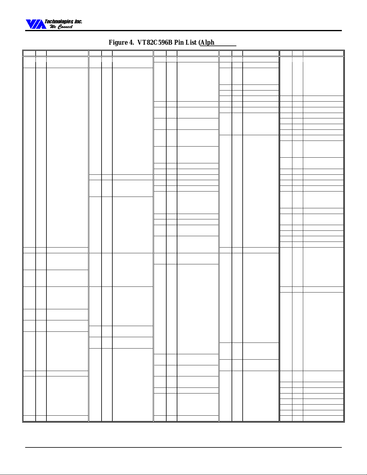
Figure 4. VT82C596B Pin List (Alphabetical Order)
Pin Pin
P01 IO A20GATE / MSCK K19 I FERR# K01 IO
M20 OD A20M# A05 IO FRAME# Y15 IO LA17 / GPO1 N20 I RCIN# D13 IO SDD10
B10 IO AD00
A10 IO AD01
D09 IO AD02
C09 IO AD03
B09 IO AD04
A09 IO AD05
D08 IO AD06
E08 IO AD07
B08 IO AD08
A08 IO AD09
D07 IO AD10
C07 IO AD11
B07 IO AD12
A07 IO AD13
D06 IO AD14
E06 IO AD15
E04 IO AD16
C04 IO AD17
B04 IO AD18
A04 IO AD19
D03 IO AD20 N01 O GNTA# / GPO9 C10 IO PCKRUN# Y09 IO SA08 D05 IO STOP#
E03 IO AD21 P02 O GNTB# / GPO10 D11 I PCLK T08 IO SA09 J18 OD STPCLK#
C03 IO AD22 P04 O GNTC# / GPO11 E10 I PCIREQA# W08 IO SA10 W20 O SUSA#
B03 IO AD23 P19 I GPI1 / PME# A11 I PCIREQB# U07 IO SA11 V19 O SUSB# / GPO15
E02 IO AD24 L02 I GPI13 / SLPBTN# B11 I PCIREQC# V07 IO SA12 U18 O SUSC# / GPO16
C02 IO AD25 J03 I GPI14 C11 I PCIREQD# Y07 IO SA13 P17 O SUSCLK
B02 IO AD26 L05 I GPI15 A01 O PCIRST# V06 IO SA14 T17 O SUSST1# / GPO20
A02 IO AD27 K03 I GPI16 R02 O PCISTP#/GPO18 Y06 IO SA15 T18 O SUSST2# / GPO21
D01 IO AD28 K04 I GPI17 L04 O PCS0# T05 IO SA16 V10 O TC
E01 IO AD29 H01 I GPI18 N05 O PCS1# W05 IO SA17 V18 I TEST#
C01 IO AD30 H04 I GPI19 G16 O PDA0 U04 IO SA18 H19 I THRM# / GPI8
B01 IO AD31 H05 I GPI20 G18 O PDA1 V04 IO SA19 C05 IO TRDY#
Y04 O AEN G03 I GPI21 G17 O PDA2 W12 IO SBHE# L03 I USBCLK
J17 O APICAK#//D1/O12 G04 O GPO00 H17 O PDCS1# V03 IO SD00 J01 I USBOC0#
H18 O APICCS#/D0/O13 T19 O GPO08 H16 O PDCS3# W03 IO SD01 J02 I USBOC1#
K18 I APICRQ#/WSC#/I5 G05 O GPO27 F20 IO PDD00 U02 IO SD02 H03 IO USBP0U10 O BALE F02 O GPO28 E18 IO PDD01 T02 IO SD03 G02 IO USBP0+
U19 I BATLOW# / GPI9 F03 O GPO29 / SCIOUT# E20 IO PDD02 W02 IO SD04 H02 IO USBP1T07 O BCLK F04 O GPO30 D18 IO PDD03 Y02 IO SD05 F01 IO USBP1+
C08 IO CBE0# A03 I IDSEL D20 IO PDD04 T01 IO SD06
C06 IO CBE1# L17 OD IGNNE# C20 IO PDD05 V01 IO SD07
D04 IO CBE2# L18 OD INIT B20 IO PDD06 W16 IO SD08
D02 IO CBE3# L19 OD INTR A20 IO PDD07 T16 IO SD09
R17 I CFG1 Y01 I IOCHCK# / GPI0 A19 IO PDD08 Y17 IO SD10
R18 I CFG2 T03 IOD IOCHRDY B19 IO PDD09 V17 IO SD11
M19 OD CPURST V12 IO IOCS16# C19 IO PDD10 Y18 IO SD12
R01 O CPUSTP# / GPO17 Y05 IO IOR# D19 IO PDD11 W18 IO SD13
U14 O DACK0# T04 IO IOW# D17 IO PDD12 Y19 IO SD14
W06 O DACK1# B05 IO IRDY# E1 9 IO PDD13 W19 IO SD15
Y10 O DACK2# H20
V05 O DACK3# J20 I IRQ1 F19 IO PDD15 B17 O SDA1
T15 O DACK5# T09 I IRQ3 G19 O PDDACK# A18 O S DA2
V16 O DACK6# W09 I IRQ4 F18 I PDDR
W17 O DACK7# U08 I IRQ5 F17 O PDIOR# C18 O SDCS3#
E05 IO DEVSEL# V08 I IRQ6 F16 O PDIOW# E15 IO SDD00
W15 I DRQ0Y08IIR
U06 I DRQ1Y20IIR
V02 I DRQ2U01IIR
U05 I DRQ3U12IIR
Y16 I DRQ5W13IIR
U16 I DRQ6T13IIR
U17 I DRQ7V14IIR
V20 IOD EXTSMI# Y14 I IRQ15 U20 I PWRBTN# D12 IO SDD08
Referenced to VCCSUS: BATLOW#, CFG1-2, EXTSMI#, GPI1, GPO8, IRQ8#, LID, PWRBTN#, PWRGD, RI#, RSMRST#, SUSA-C#, SUSST1-2#, TEST#
m
Pin Pin
D10 P GND
E07 P GND
E13 P GND
J09 P GND
J10 P GND
J11 P GND
J12 P GND
K09 P GND
K10 P GND
K11 P GND
K12 P GND
L09 P GND
L10 P GND
L11 P GND
L12 P GND
M09 P GND
M10 P GND
M11 P GND
M12 P GND
J05 P GNDUSB
IRQ0OUT / GPO14 E17 IO PDD14 C17 O SDA0
O
7 A12 I PGNT# B15 IO SDD01
8# / GPI6 B12 O PREQ# D14 IO SDD02
9 G20 I PDRDY C14 IO SDD03
10 R03 IOD PIRQA# A14 IO SDD04 M03 O XDIR# / GPO22
11 R04 IOD PIRQB# C13 IO SDD05 M04 O XOE# / GPO23
12 P05 IOD PIRQC# A13 IO SDD06 Y03 I ZWS#
14 G01 IOD PIRQD# C12 IO SDD07 K16 O ZZ / GPO19
m
Pin Pin
T14 IO LA18 / GPO2 M01 I REQA# / GPI2 B14 IO SDD11
W14 IO LA19 / GPO3 N02 I REQB# / GPI3 E14 IO SDD12
U13 IO LA20 / GPO4 P03 I REQC# / GPI4 A15 IO SDD13
V13 IO LA21 / GPO5 W07 IO RFSH# C15 IO SDD14
Y13 IO LA22 / GPO6 P18 I RI# / GPI12 D15 IO SDD15
T12 IO LA23 / GPO7 K02 O ROMCS# A17 O SDDACK#
P16 I LID / GPI10 M17 I RSMRST# A16 I SDDR
N04 O MC CS# W01 O RSTDRV C16 O SDIOR#
Y12 IO MCS16# L01 O RTCAS/GPO25 B16 O SDIOW#
V15 IO MEMR# M02 O RTCCS#/GPO24 J19 I SERIRQ / GPI7
U15 IO MEMW# N19 I RTCX1 A06 I SERR#
J04 I NC / KEYLOCK R20 O RTCX2 D16 I SDRDY
M05 IO NC / KBDT U11 IO SA00 K20 OD SLP#
N03 IO NC / KBCK T11 IO SA01 N17 I SMBALRT#/GPI11
M16 - NC W11 IO SA02 R19 IO SMBCLK
N18 - NC Y11 IO SA03 T20 IO SMBDATA
R05 - NC T10 IO SA04 W04 O SMEMR#
L20 OD NMI W10 IO SA05 U03 O SMEMW#
V11 I OSC U09 IO SA06 P20 OD SMI#
B06 O PAR V09 IO SA07 K17 O SPKR
m
KBCS#/GPO26/MSDT
Pin Pin
M18 I PWRGD B13 IO SDD09
B18 O SDCS1#
m
Pin Pin
L16 P VBAT
E09 P VCC
E11 P VCC
E12 P VCC
E16 P VCC
F05 P VCC
F06 P VCC
F14 P VCC
F15 P VCC
G06 P VCC
P15 P VCC
R06 P VCC
R07 P VCC
R15 P VCC
T06 P VCC
N16 P VCCSUS
R16 P VCCSUS
K05 P VCCUSB
J16 P VREF
m
Revision 0.3 June 17, 1999 -6- Pinouts
Page 13
7HFKQRORJLHV ,QF
&
:H&RQQHFW
RQQHFW
:H
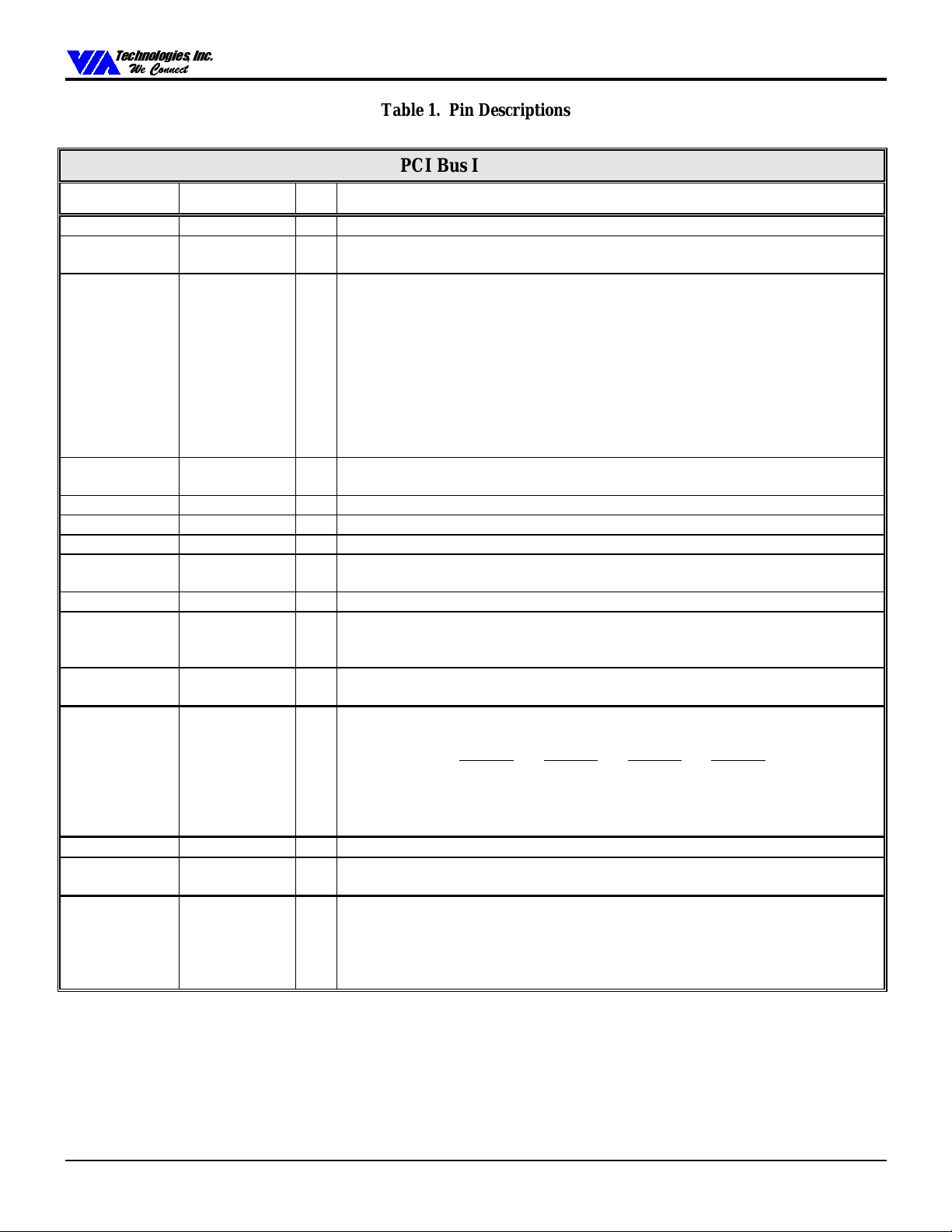
Table 1. Pin Descriptions
PCI Bus Interface
Signal Name Pin # I/O Signal Description
VT82C596B
PCLK
FRAME#
AD[31:0]
C/BE[3:0]#
IRDY#
TRDY#
STOP#
DEVSEL#
PAR
SERR#
IDSEL
PIRQA-D#
PREQ#
PGNT#
PCKRUN#
D11 I
A5 IO
B1, C1, E1,
D1, A2, B2,
C2, E2, B3, C3,
E3, D3, A4,
B4, C4, E4, E6,
D6, A7, B7,
C7, D7, A8,
B8, E8, D8,
A9, B9, C9,
D9, A10, B10
D2, D4, C6, C8 IO
B5 IO
C5 IO
D5 IO
E5 IO
B6 IO
A6 I
A3 I
R3, R4, P5, G1 I
B12 O
A12 I
C10 IO
IO
PCI Clock.
Frame.
that one more data transfer is desired by the cycle initiator.
Address/Data Bus.
with FRAME# assertion and data is driven or received in following cycles.
Comma nd/By te Ena ble.
enables corresponding to supplied or requested data are driven on following clocks.
Initiator Ready.
Target Ready.
Stop.
Device Select.
positive or subtractive decoding.
Parity.
System Error.
error condition. Upon sampling SERR# active, the VT82C596B can be programmed
to generate an NMI to the CPU.
Initialization Device Select.
configuration read and write cycles.
PCI Interrupt Request
INTD# pins as follows:
PCI Slot 1 INTA# INTB# INTC# INTD#
PCI Slot 2 INTB# INTC# INTD# INTA#
PCI Slot 3 INT C# INTD# INTA# INTB#
PCI Slot 4 INTD# INTA# INTB# INTC#
PCI Request.
PCI Grant.
VT82C596B.
PCI Bus Clock Run.
stopped (high) or running (low). The VT82C596B drives this signal low when the
PCI clock is running (de fault on reset) and releases it when it stops the PCI clock.
External devices may assert this signal low to request that the PCI clock be restarted
or prevent it from stopping. Refer to the PCI Mobile Design Guide for more details.
PCLK provides timing for all transactions on the PCI Bus.
Assertion indicates the address phase of a PCI transfer. Negation indicates
The standard PCI address and data lines. The address is driven
The command is driven with FRAME# assertion. Byte
Asserted when the initiator is ready for data transfer.
Asserted when the target is ready for data transfer.
Asserted by the target to request the master to stop the current transaction.
The VT82C596B asserts this signal to claim PCI transactions through
A single parity bit is provided over AD[31:0] and C/BE[3:0]#.
SERR# can be pulsed active by any PCI device that detects a system
IDSEL is used as a chip select during PCI
. These pins are typically connected to the PCI bus INTA#-
PIRQA# PIRQB#
This signal goes to the North Bridge to req uest the PCI bus.
This signal is driven by the North Bridge to grant PCI access to the
This signal indicates whether the PCI clock is or will be
PIRQC# PIRQD#
Revision 0.3 June 17, 1999 -7- Pinouts
Page 14
7HFKQRORJLHV ,QF
&
:H&RQQHFW
RQQHFW
:H
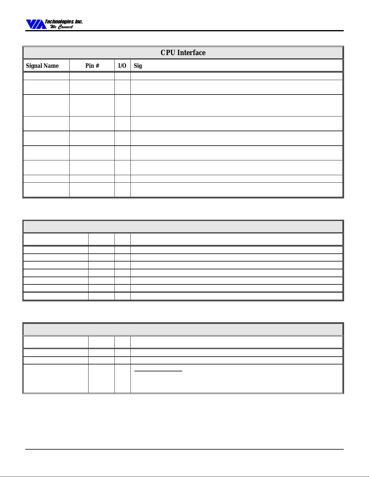
CPU Interface
Signal Name Pin # I/O Signal Description
VT82C596B
CPURST
INTR
NMI
INIT
STPCLK#
SMI#
FERR#
IGNNE#
SLP#
M19 OD
L19 OD
L20 OD
L18 OD
J18 OD
P20 OD
K19 I
L17 OD
K20 OD
CPU Reset.
CPU Interrupt.
interrupt request is pending and needs service.
Non-Maskable Interrupt.
CPU. The VT82C596B generates an NMI when either SERR# or IOCHK# is
asserted.
Initialization.
on the PCI bus or if a soft reset is initiated by the register
Stop Clock.
different Power-Management events.
System Management Interrupt.
in response to different Power-Management events.
Numerical Coprocessor Error.
the CPU. Internally generates interrupt 13 if active.
Ignore Numeric Error.
Sleep.
used with socket-7 CPUs.
The VT82C596B asserts CPURST to reset the CPU during power-up.
INTR is driven by the VT82C596B to signal the CPU that an
The VT82C596B asserts INIT if it detects a shut-down special cycle
STPCLK# is asserted by the VT82C596B to the CPU in response to
Used to put the CPU to sleep. Used with slot-1 CPUs only. Not currently
Universal Serial Bus Interface
Signal Name Pin # I/O Signal Description
USBP0+
USBP0USBOC0#
USBP1+
USBP1USBOC1#
USBCLK
G2 IO
H3 IO
J1 I
F1 I O
H2 IO
J2 I
L3 I
USB Port 0 Data +
USB Port 0 Data USB Port 0 Over Current Detect.
USB Port 1 Data +
USB Port 1 Data USB Port 1 Over Current Detect.
USB Clock.
48MHz clock input for Universal Serial Bus interface
NMI is used to force a non-maskable interrupt to the
SMI# is asserted by the VT82C596B to the CPU
This signal is tied to the coprocessor error signal on
This pin is connected to the “ignore error” pin on the CPU.
Port 0 is disabled if this input is low.
Port 1 is disabled if this input is low.
System Management Bus (SMB) Interface (I2C Bus)
Signal Name Pin # I/O Signal Description
SMBCLK
SMBDATA
SMBALRT#
Revision 0.3 June 17, 1999 -8- Pinouts
/ GPI11
R19 IO
T20 IO
N17 I
SMB / I2C Clock.
SMB / I2C Data.
MultiFunction Pin
SMB Alert.
an IRQ or SMI interrupt or a power management resume event.
General Purpose Input 11.
(Rx74[5] = 0) When the chip is enabled to allo w it, assertion generates
(Rx74[5] = 1) General purpose input.
Page 15
7HFKQRORJLHV ,QF
&
:H&RQQHFW
RQQHFW
:H
UltraDMA-33 / 66 Enhanced IDE Interface
Signal Name Pin # I/O Signal Description
VT82C596B
PDRDY /
PDDMARDY# /
PDSTROBE
SDRDY /
SDDMARDY# /
SDSTROBE
PDIOR# /
PHDMARDY# /
PHSTROBE
SDIOR# /
SHDMARDY# /
SHSTROBE
PDIOW# /
PSTOP
SDIOW# /
SSTOP
PDDRQ
SDDRQ
PDDACK#
SDDACK#
G20 I
D16 I
F17 O
C16 O
F16 O
B16 O
F18 I
A16 I
G19 O
A17 O
EIDE Mode:
UltraDMA Mode:
EIDE Mode:
UltraDMA Mode:
EIDE Mode:
UltraDMA Mode:
EIDE Mode:
UltraDMA Mode:
EIDE Mode:
UltraDMA Mode:
EIDE Mode:
UltraDMA Mode:
Primary Device DMA Request.
Secondary Device DMA Request.
Primary Device DMA Acknowledge.
Secondary Device DMA Acknowledge.
Primary I/O Channel Ready.
Primary Device DMA Ready
may assert PDDMARDY# to pause output transfers
Primary Device Strobe
device may stop PDSTROBE to pause input data transfers
Secondary I/O Channel Ready.
Secondary Device DMA Ready
device may assert SDDMARDY# to pause output transfers
Secondary Device Strobe
device may stop SDSTROBE to pause input data transfers
Primary Device I/O Read.
Primary Host DMA Ready
The host may assert PHDMARDY# to pause input transfers
Primary Host Strobe
host may stop PHSTROBE to pause output data transfers
Secondary Device I/O Read.
Secondary Host DMA Ready
may assert SHDMARDY# to pause input transfers
Host Strobe B
SHSTROBE to pause output data transfers
Primary Device I/O Write.
Primary Stop
initiation of an UltraDMA burst; negated by the host before data
is transferred in an UltraDMA burst. Assertion of STOP by the
host during or after data transfer in UltraDMA mode signals the
termination of the burst.
Secondary Device I/O Write.
Secondary Stop
initiation of an UltraDMA burst; negated by the host before data
is transferred in an UltraDMA burst. Assertion of STOP by the
host during or after data transfer in UltraDMA mode signals the
termination of the burst.
. Output strobe (both edges). The host may stop
. Stop transfer: Asserted by the host prior to
. Stop transfer: Asserted by the host prior to
Primary channel DMA request
Secondary channel DMA request
Primary channel DMA acknowledge
Device ready indicator
. Output flow control. The device
. Input data strobe (both edges). The
Device ready indicator
. Output flow control. The
. Input data strobe (both edges). The
Device read strobe
. Primary channel input flow control
. Output data strobe (both edges). The
Device read strobe
. Input flow control. The host
Device write strobe
Device write strobe
Secondary channel DMA acknowledge
.
Revision 0.3 June 17, 1999 -9- Pinouts
Page 16
7HFKQRORJLHV ,QF
&
:H&RQQHFW
RQQHFW
:H
UltraDMA-33 / 66 Enhanced IDE Interface (continued)
Signal Name Pin # I/O Signal Description
VT82C596B
PDCS1#
PDCS3#
SDCS1#
SDCS3#
PDA[2-0]
SDA[2-0]
PDD[15-0]
SDD[15-0]
H17 O
H16 O
B18 O
C18 O
G17, G18,
G16
A18, B17,
C17
F19, E17,
E19, D17,
D19, C19,
B19, A19,
A20, B20,
C20, D20,
D18, E20,
E18, F20
D15, C15,
A15, E14,
B14, D13,
B13, D12,
C12, A13,
C13, A14,
C14, D14,
B15, E15
Primary Master Chip Select.
IDE connector.
Primary Slave Chip Select.
IDE connector.
Secondary Master Chip Select.
secondary IDE connector.
Secondary Slave Chip Select.
IDE connector.
O
Primary Disk Address.
command block or control block is being accessed.
O
Secondary Disk Address.
ATA command block or control block is being accessed.
IO
Primary Disk Data
IO
Secondary Disk Data
This signal corresponds to CS1FX# on the primary
This signal corresponds to CS3FX# on the primary
This signal corresponds to CS17X# on the
This signal corresponds to CS37X# on the secondary
PDA[2:0] are used to indicate which byte in either the ATA
SDA[2:0] are used to indicate which byte in either the
Revision 0.3 June 17, 1999 -10- Pinouts
Page 17
7HFKQRORJLHV ,QF
&
:H&RQQHFW
RQQHFW
:H
ISA Bus Interface
Signal Name Pin # I/O Signal Description
VT82C596B
SA[19:0]
LA[23:17]
SD[15:0]
SBHE#
IOR#
IOW#
MEMR#
MEMW#
SMEMR#
SMEMW#
BALE
IOCS16#
MCS16#
IOCHCK#
IOCHRDY
ZWS#
V4, U4, W5,
T5, Y6, V6,
Y7, V7, U7,
W8, T8, Y9,
V9, U9, W10,
T10, Y11,
W11, T11, U11
T12, Y13, V13,
U13, W14,
T14, Y15
W19, Y19,
W18, Y18,
V17, Y17, T16,
W16, V1, T1,
Y2, W2, T2,
U2, W3, V3
W12 IO
Y5 IO
T4 IO
V15 IO
U15 IO
W4 O
U3 O
U10 O
V12 IO
Y12 IO
Y1 I
T3 IOD
Y3 I
IO
ISA Address Bus
IO
ISA “Latched” Address Bus
These address lines allow accesses to physical memory on the ISA bus up to
16Mbytes.
IO
ISA Bus Data.
SD7:4 are strap options for keyboard inputs 6:3 (see Function 0 Rx5A)
ISA Byte High Enable.
transferred on the upper byte (SD[15:8]) of the data bus. SBHE# is negated during
refresh cycles.
ISA I/O Read.
that the slave may drive data on to the ISA data bus.
ISA I/O Write.
that the slave may latch data from the ISA data bus.
ISA Memory Read.
that it may drive data onto the ISA data bus.
ISA Memory Write.
that it may latch data from the ISA data bus.
ISA Standard Memory Read.
under 1MB, which indicates that it may drive data onto the ISA data bus
ISA Standard Memory Write.
under 1MB, which indicates that it may latch data from the ISA data bus.
ISA Bus Address Latch Enable.
VT82C596B to indicate that the address (SA[19:0], LA[23:17] and the SBHE#
signal) is valid
ISA 16-Bit I/O Chip Select.
indicate that they support 16-bit I/O bus cycles.
ISA Memory Chip Select 16.
line low to indicate they support 16-bit memory bus cycles.
ISA I/O Channel Check.
an uncorrectable error has occurred for a device or memory on the ISA Bus.
ISA I/O Channel Ready.
assert IOCHRDY low to indicate that additional time (wait states) is required to
complete the cycle.
ISA Zero Wait State.
states are required.
SD[15:0] provide the data path fo r devices residing on the ISA bus.
IOR# is the command to an ISA I/O slave device which indicates
IOW# is the command to an ISA I/O slave device which indicates
MEMR# is the command to a memory slave which indicates
MEMW# is the command to a memory slave which indicates
: The LA[23:17] address lines are bi-directional.
SBHE# indicates, when asserted, that a byte is being
SMEMR# is the command to a memory slave,
SMEMW# is the command to a memory slave,
BALE is an active high signal asserted by the
This signal is driven by I/O devices on the ISA Bus to
ISA slaves that are 16-bit memory devices drive this
When this signal is asserted, it indicates that a parity or
This signal is normally high. Devices on the ISA Bus
Devices on the ISA Bus assert ZWS# to indicate that no wait
Revision 0.3 June 17, 1999 -11- Pinouts
Page 18
7HFKQRORJLHV ,QF
&
:H&RQQHFW
RQQHFW
:H
ISA Bus Interface (continued)
Signal Name Pin # I/O Signal Description
VT82C596B
RFSH#
AEN
IRQ0OUT
GPO14
IRQ1
IRQ3
IRQ4
IRQ5
IRQ6
IRQ7
IRQ8#
IRQ9
IRQ10
IRQ11
IRQ12
IRQ14
IRQ15
DRQ7-5, 3-0
DACK7-5, 3-0#
TC
SPKR
/
/ GPI6
W7 IO
Y4 O
H20 O
J20 I
T9 I
W9 I
U8 I
V8 I
Y8 I
Y20 I
U1 I
U12 I
W13 I
T13 I
V14 I
Y14 I
U17, U16,
Y16, U5, V2,
U6, W15
W17, V16,
T15, V5, Y10,
W6, U14
V10 O
K17 O
Refresh.
input RFSH# is driven by 16-bit ISA Bus masters to indicate refresh cycle.
Address Enable.
misinterpreting DMA cycles as valid I/O cycles.
Multifunction Pin
Interrupt Request 1.
Interrupt Request 3.
Interrupt Request 4.
Interrupt Request 5.
Interrupt Request 6.
Interrupt Request 7.
Multifunction Pin
Interrupt Request 9.
Interrupt Request 10.
Interrupt Request 11.
Interrupt Request 12.
Interrupt Request 14.
Interrupt Request 15.
I
DMA Request.
O
Acknowledge.
DMA service has been granted.
Terminal Count.
Speaker Drive.
As an output RFSH# indicates when a refresh cycle is in progress. As an
AEN is asserted during DMA cycles to prevent I/O slaves from
Rx74[7] = 1
Rx74[7] = 0
Rx5A[2] = 0 Internal RTC disabled.
Rx5A[2] = 1 Internal RTC enabled.
Interrupt Request 0 Output.
system timer IRQ0 signal.
General Purpose Output 14
Used to request DMA services from the internal DMA controller.
Used by the internal DMA controller to indicate that a request for
Asserted to DMA slaves as a terminal count indicator.
The output of internal timer/counter 2.
General Purpose Input 6
Reflects the state of the internal
.
Interrupt Request 8
from external RTC
.
Revision 0.3 June 17, 1999 -12- Pinouts
Page 19
7HFKQRORJLHV ,QF
&
:H&RQQHFW
RQQHFW
:H
XD Interface
Signal Name Pin # I/O Signal Description
VT82C596B
XDIR#
XOE#
KBCS#
ROMCS#
MCCS#
PCS[1-0]#
/ GPO22
/ GPO23
/ GPO26
M3 O
M4 O
K1 O
K2 O
N4 O
N5, L4 O
MultiFunction Pin
X-Bus Data Direction.
memory read cycles to the programmed BIOS or APIC address space. XDIR# is
tied directly to the direction control of a 74F245 transceiver that buffers the X-Bus
data and ISA-Bus data. SD0-7 connect to the “A” side of the transceiver and
XD0-7 connect to the “B” side. XDIR# high indicates that SD0-7 drives XD0-7.
General Purpose Output 22.
MultiFunction Pin
X-Bus Output Enable.
XOE# is tied directly to the output enable of a 74F245 transceiver that buffers the
X-Bus data and ISA-Bus data (see XDIR# above).
General Purpose Output 23.
MultiFunction Pin
External Keyboard Controller Chip Select.
or write accesses to I/O ports 60h and 64h.
General Purpose Output 26.
ROM Chip Select.
Microcontroller Chip Select.
62h or 66h.
Programmable Chip Selects.
write ISA address ranges. Devices selected by these pins are assumed to be on the XBus (XDIR# and XOE# are enabled).
(Rx75[6]=0) Asserted low for all I/O read cycles and for
(Rx75[6]=1) General purpose output.
(Rx75[6]=0) Asserted low for all decoded X-Bus cycles.
(Rx75[6]=1) General purpose output.
(Rx76[2] = 0) Asserted during read
(Rx76[2]=1) General purpose output.
Chip Select to the BIOS ROM.
Asserted during read or write accesses to I/O ports
Asserted during I/O cycles to programmable read or
Revision 0.3 June 17, 1999 -13- Pinouts
Page 20
7HFKQRORJLHV ,QF
&
:H&RQQHFW
RQQHFW
:H
Internal Real Time Clock
Signal Name Pin # I/O Signal Description
VT82C596B
RTCX1
RTCX2
RTCCS#
RTCAS
/ GPO24
/ GPO25
N19 I
R20 O
M2 O
L1 O
RTC Crystal Input
RTC Crystal Output
MultiFunction Pin
External RTC Chip Select.
RTC port 71h. Externally connected to a pair of OR gates (to logically AND
the chip select with IOR# and IOW#) to generate the active-low RTC read and
write commands.
General Purpose Output 24.
MultiFunction Pin
External RTC Address Strobe.
Port 70h.
General Purpose Output 25.
Internal Keyboard Controller
Signal Name Pin # I/O Signal Description
KEYLOCK
/ NC
KBCK
/ NC
KBDT
/ A20GATE
MSCK
/ KBCS# / GPO26
MSDT
/ PIRQ1
J4 I
N3 IO
M5 IO
P1 IO
K1 IO
Extended Function
Rx59[1]=1
Key Lock.
Extended Function
Rx5A[0]=1 (Internal keyboard controller enabled –strapped from XD0)
Keyboard Clock
Extended Function
Rx5A[0]=1 (Internal keyboard controller enabled –strapped from XD0)
Keyboard Data
MultiFunction Pin
Rx5A[1]=0 (internal keyboard controller disabled – strapped from XD1)
Gate A20.
Rx5A[1]=1 (internal keyboard controller enabled
Mouse Clock.
MultiFunction Pin
Rx5A[1]=0 (Internal keyboard controller disabled –strapped from XD1)
Keyboard Controller Chip Select.
enabled) Chip select for external keyboard controller.
General Purpose Output 26
disabled) General purpose output
Rx5A[1]=1 (Internal keyboard controller enabled –strapped from XD1)
Mouse Data.
Input to internal keyboard controller
From optional external keyboard controller
Mouse clock (exte nded function not available on PIIX4)
Mouse data (extended function not available on PIIX4)
: 32.768 KHz crystal or oscillator input.
: 32.768 KHz crystal output
(Rx76[0] = 0) Asserted for read or write accesses to
(Rx76[0] = 1) General purpose output.
(Rx76[1] = 0) Asserted for writes to RTC I/O
(Rx76[1] = 1) General purpose output.
(PIIX4 PIRQ1)
(PIIX4 No Connect)
(PIIX4 No Connect)
–strapped from XD1)
(Rx76[2]=0 external keyboard controller
(Rx76[2]=1 external keyboard controller
Revision 0.3 June 17, 1999 -14- Pinouts
Page 21
7HFKQRORJLHV ,QF
&
:H&RQQHFW
RQQHFW
:H
PC/PCI and Serial IRQ Control
Signal Name Pin # I/O Signal Description
VT82C596B
REQ[A-C]#
GNT[A-C]#
SERIRQ
/ GPI7
/ GPI[2-4]
/ GPO[9-11]
M1, N2, P3 I
N1, P2, P4 O
J19 I
PC/PCI DMA Requests.
per the PC/PCI protocol. For GPI functions refer to Rx7D[2-0].
PC/PCI DMA Grants.
PC/PCI protocol. For GPO functions refer to Rx7D[2-0].
Serial Interrupt Request.
Rx68[3].
A20 Control
Signal Name Pin # I/O Signal Description
A20GATE
A20M#
/ MSCK
P1 I
M20 OD
Gate A20:
if used. Logically combined with Port 92 bit-1 (Fast_A20) and output
on the A20M# signal. If the internal keyboard / PS2 mouse co ntroller is
used, this pin becomes the mouse clock input (the A20GATE signal
comes directly from the internal keyboard controller).
A20 Mask.
Gate A20 output from optional external keyboard controller
Connect to A20 mask input of the CPU.
APIC Interface
Signal Name Pin # I/O Signal Description
APICREQ#
APICCS#
APICACK#
/ APICD0 / GPO13
/ WSC# / GPI5
/ APICD1 / GPO12
K18 I / I / I
H18 O / O / O
J17 O / O / O
MultiFunction Pin
Internal APIC Write Snoop Complete.
Asserted by the north bridge to indicate that all snoop activity on the
CPU bus initiated by the last PCI-to-DRAM write is complete and
that it is safe to perform an APIC interrupt.
External APIC Request.
external APIC synchronous to PCICLK prior to sending an interrupt
over the APIC serial bus. This signals the VT82C596B to flush its
internal buffers.
General Purpose Input 5.
MultiFunction Pin
Internal APIC Data 0.
External APIC Chip Select.
VT82C596B drives this signal active to select an external APIC (if
used). This occurs if the external APIC is enabled and a PCI cycle is
detected within the programmed APIC address range.
General Purpose Output 13.
MultiFunction Pin
Internal APIC Data 1.
External APIC Acknowledge.
the VT82C596B to indicate that it internal buffers have been flushed
(in response to APICREQ#). This indicates to the external APIC that
the VT82C596B’s internal buffers have been flushed and that it is OK
for the APIC to send its interrupt.
General Purpose Output 12.
Used by PCI agent to request DMA services
Used to acknowledge DMA services per the
Used with Distributed DMA. For GPI see
(Rx74[7]=1 & Rx74[1]=1)
(Rx74[7]=1 & Rx74[1]=0) Asserted by
(Rx74[7] = 0)
(Rx74[7]=1 & Rx74[1]=1)
(Rx74[7]=1 & Rx74[1]=0) The
(Rx74[7] = 0)
(Rx74[7]=1 & Rx74[1]=1)
(Rx74[7]=1 & Rx74[1]=0) Asserted by
(Rx74[7] = 0)
Revision 0.3 June 17, 1999 -15- Pinouts
Page 22
7HFKQRORJLHV ,QF
&
:H&RQQHFW
RQQHFW
:H
General Purpose Inputs
Signal Name Pin # I/O Signal Description
VT82C596B
/ IOCHCK#
GPI0
/ PME#
GPI1
/ REQA#
GPI2
/ REQB#
GPI3
/ REQC#
GPI4
/ APICREQ#
GPI5
/ IRQ8#
GPI6
/ SERIRQ
GPI7
/ THRM#
GPI8
/ BATLOW#
GPI9
/ LID
GPI10
/ SMBALRT#
GPI11
/ RI#
GPI12
/ SLPBTN#
GPI13
GPI14
GPI15
GPI16
GPI17
GPI18
GPI19
/ PIRQ0
GPI20
/ PIRQ2
GPI21
The underlined name above indicates the default function on power up.
Y1 I
P19 I
M1 I
N2 I
P3 I
K18 I
Y20 I
J19 I
H19 I
U19 I
P16 I
N17 I
P18 I
L2 I
J3 I
L5 I
K3 I
K4 I
H1 I
H4 I
H5 I
G3 I
General Purpose Input 0.
General Purpose Input 1.
General Purpose Input 2.
General Purpose Input 3.
General Purpose Input 4.
General Purpose Input 5.
General Purpose Input 6.
General Purpose Input 7.
General Purpose Input 8.
General Purpose Input 9.
General Purpose Input 10.
General Purpose Input 11.
General Purpose Input 12.
General Purpose Input 13.
register 0 of ACPI I/O Space (Function 3) is enabled
General Purpose Input 14.
General Purpose Input 15.
General Purpose Input 16.
General Purpose Input 17.
General Purpose Input 18.
General Purpose Input 19.
General Purpose Input 20.
General Purpose Input 21.
(Rx74[0] = 0)
(Rx7D[0] = 0)
(Rx7D[1] = 0)
(Rx7D[2] = 0)
(Rx74[7] = 0)
(Rx5A[2] = 1)
(Rx68[3] = 0)
(Rx74[2] = 1)
(Rx74[3] = 1)
(Rx74[4] = 1)
(Rx74[5] = 1)
(Rx74[6] = 1)
Also functions as the ACPI sleep button if bit-9 of
(Rx59[0] = 1) See also Rx55[3:0]
(Rx59[2] = 1) See also Rx58[3:0]
Revision 0.3 June 17, 1999 -16- Pinouts
Page 23

7HFKQRORJLHV ,QF
&
:H&RQQHFW
RQQHFW
:H
General Purpose Outputs
Signal Name Pin # I/O Signal Description
VT82C596B
GPO0
/ LA17
GPO1
/ LA18
GPO2
/ LA19
GPO3
/ LA20
GPO4
/ LA21
GPO5
/ LA22
GPO6
/ LA23
GPO7
GPO8
/ GNTA#
GPO9
GPO10
GPO11
GPO12
GPO13
GPO14
GPO15
GPO16
GPO17
GPO18
GPO19
GPO20
GPO21
GPO22
GPO23
GPO24
GPO25
GPO26
GPO27
GPO28
GPO29
GPO30
The underlined name above indicates the default function on power up.
/ GNTB#
/ GNTC#
/ APICACK#
/ APICCS#
/ IRQ0OUT
/ SUSB#
/ SUSC#
/ CPUSTP#
/ PCISTP#
/ ZZ
/ SUSST1#
/ SUSST2#
/ XDIR#
/ XOE#
/ RTCCS#
/ RTCAS
/ KBCS#
/ SCIOUT#
G4 O
Y15
T14
W14
U13
V13
Y13
T12
T19 O
N1 O
P2 O
P4 O
J17 O
H18 O
H20 O
V19 O
U18 O
R1 O
R2 O
K16 O
T17 O
T18 O
M3 O
M4 O
M2 O
L1 O
K1 O
G5 O
F2 O
F3 O
F4 O
General Purpose Output 0.
IO General Purpose Output 1.
IO General Purpose Output 2.
IO General Purpose Output 3.
IO General Purpose Output 4.
IO General Purpose Output 5.
IO General Purpose Output 6.
IO General Purpose Output 7.
General Purpose Output 8.
General Purpose Output 9.
General Purpose Output 10.
General Purpose Output 11.
General Purpose Output 12.
General Purpose Output 13.
General Purpose Output 14.
General Purpose Output 15.
General Purpose Output 16.
General Purpose Output 17.
General Purpose Output 18.
General Purpose Output 19.
General Purpose Output 20.
General Purpose Output 21.
General Purpose Output 22.
General Purpose Output 23.
General Purpose Output 24.
General Purpose Output 25.
General Purpose Output 26.
General Purpose Output 27.
General Purpose Output 28.
General Purpose Output 29.
General Purpose Output 30.
Rx74[0] = 0.
Rx74[0] = 0.
Rx74[0] = 0.
Rx74[0] = 0.
Rx74[0] = 0.
Rx74[0] = 0.
Rx74[0] = 0.
F3Rx54[1-0]. Optional 1Hz / 2Hz / 4Hz clock output
Rx7D[0] = 0.
Rx7D[1] = 0.
Rx7D[2] = 0.
Rx74[7] = 0.
Rx74[7] = 0.
Rx74[7] = 0.
Rx75[0] = 1. See also F3Rx54[3].
Rx75[0] = 1. See also F3Rx54[2].
Rx75[1] = 1.
Rx75[2] = 1.
Rx75[3] = 1.
Rx75[4] = 1. See also F3Rx54[4].
Rx75[5] = 1. See also F3Rx54[7].
Rx75[6] = 1.
Rx75[6] = 1.
Rx76[0] = 1.
Rx76[1] = 1.
Rx76[2] = 1.
Rx74[7] = 0.
Revision 0.3 June 17, 1999 -17- Pinouts
Page 24
7HFKQRORJLHV ,QF
&
:H&RQQHFW
RQQHFW
:H
Power Management
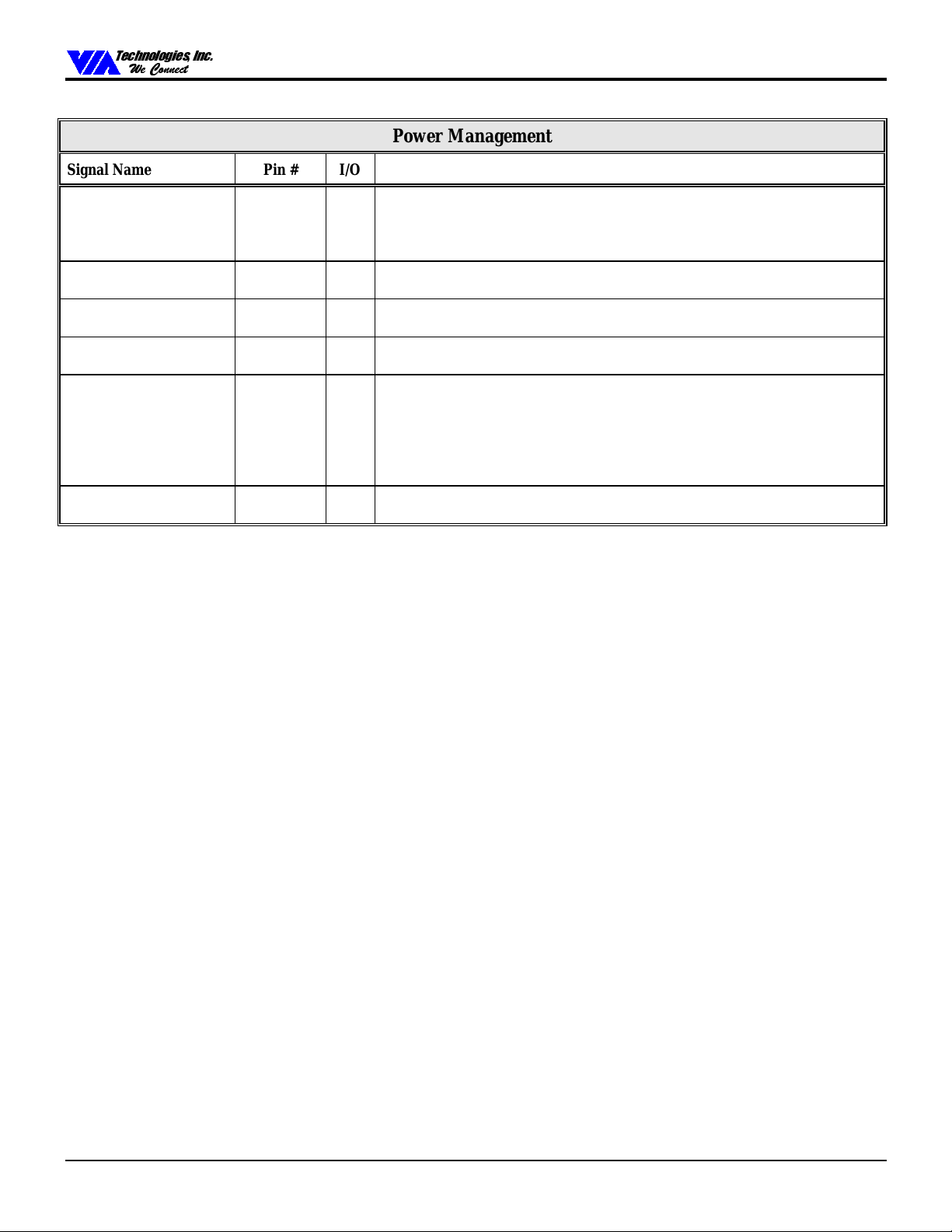
Signal Name Pin # I/O Signal Description
VT82C596B
PWRBTN#
SLPBTN#
RCIN#
RSMRST#
EXTSMI#
PCIREQ[A-D]#
/ GPI13
U20 I
L2 I
N20 I
M17 I
V20 IOD
E10, A11,
B11, C11
Power Button.
external system on/off button or switch. The VT82C596B performs a 200us
debounce of this input if Rx40[5] is set to 1. This input is referenced to
VCCSUS.
ACPI Sleep Button.
sleep button if bit-9 of register 0 of ACPI I/O Space (Function 3) is enabled.
Reset CPU.
used) causes an INIT signal to be generated to the CPU.
Resume Reset.
plane and also resets portions of the internal RTC logic.
External System Management Interrupt.
edge on this input causes an SMI# to be generated to the CPU to enter SMI
mode. Once asserted, this pin should be held low for at least four PCICLKs.
The VT82C596B also asserts EXTSMI# in response to SMI# being activated
within the Serial IRQ function. This pin should be connected to an external
pullup.
I
Power Management PCI Requests.
monitor PCI requests for use of the PCI bus.
Used by the Power Management subsystem to monitor an
General purpose input 13, but also functions as the ACPI
This signal from an optional external keyboard controller (if
Resets the internal logic connected to the VCCSUS power
When enabled to allow it, a falling
Used by internal power management to
Revision 0.3 June 17, 1999 -18- Pinouts
Page 25
7HFKQRORJLHV ,QF
&
:H&RQQHFW
RQQHFW
:H
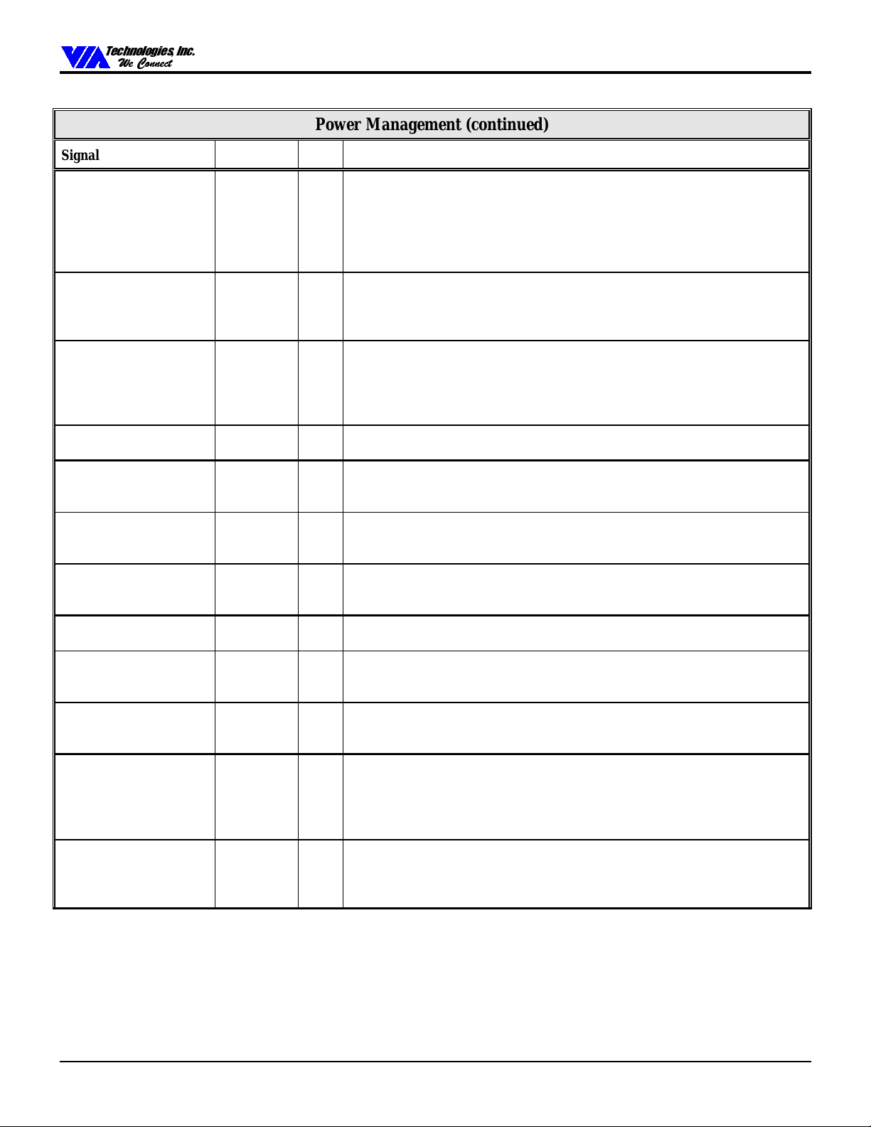
Power Management (continued)
Signal Name Pin # I/O Signal Description
VT82C596B
/ GPI10
LID
/ GPI12
RI#
THRM#
SCIOUT#
CPUSTP#
PCISTP#
/ GPO19
ZZ
SUSA#
/ GPO15
SUSB#
SUSC#
SUSST1#
SUSST2#
/ GPO16
/ GPI8
/ GPO29
/ GPO17
/ GPO18
/ GPO20
/ GPO21
P16 I
P18 I
H19 I
F3 O
R1 O
R2 O
K16 O
W20 O
V19 O
U18 O
T17 O
T18 O
Notebook Computer Display Lid Open / Closed Monitor.
Power Management subsystem to monitor the opening and closing of the
display lid of notebook computers. Can be used to detect either low-to-high
and/or high-to-low transitions to generate an SMI#. The VT82C596B
performs a 200 usec debounce of this input if Rx40[5] is set to 1. May
optionally be programmed as a general purpose input (Rx74[4]=1).
Ring Indicator.
system to be re-activated by a received phone call. This input is referenced to
VCCSUS. May optionally be programmed as a general purpose input
(Rx74[6]=1).
Thermal Detect.
signal initiates hardware Clock Throttling mode. This causes STPCLK# to be
cycled at a preset programmable rate (see Function 3 configuration space
Rx4C). May optionally be programmed as a general purpose input
(Rx74[2]=1).
ACPI System Control Interrupt.
May optionally be programmed as a general purpose output (Rx74[7]=0).
CPU Clock Stop.
outputs. May optionally be programmed as a general purpose output
(Rx75[1]=1).
PCI Clock Stop.
outputs. May optionally be programmed as a general purpose output
(Rx75[2]=1).
L2 Cache SRAM Low Power Mode.
SRAMs during CPU Stop Clock state. May optionally be programmed as a
general purpose output (Rx75[3]=1).
Suspend Plane A Control.
and STD suspend states. Used to control the primary power plane.
Suspend Plane B Control.
suspend states. Used to control the secondary power plane. May optionally be
programmed as a general purpose output (Rx75[0]=1).
Suspend Plane C Control.
state. Used to control the tertiary power plane. May optionally be
programmed as a general purpose output (Rx75[0]=1).
Suspend Status 1.
Apollo MVP3) to provide information on host clock status. Asserted when the
system may stop the host clock, such as Stop Clock or during POS, STR, or
STD suspend states. May optionally be programmed as a general purpose
output (Rx75[4]=1).
Suspend Status 2.
information on system suspend state. Asserted during POS, STR, or STD
suspend states. May optionally be programmed as a general purpose output
(Rx75[5]=1).
May be connected to external modem circuitry to allow the
If the VT82C596B is enabled to allow it, asserting this
Connected to the external APIC if used.
Signals the system clock generator to disable the CPU clock
Signals the system clock generator to disable the PCI clock
Used to power down the L2 Cache
Asserted during po wer management POS, STR,
Asserted during power management STR and STD
Asserted during p ower manage ment ST D susp end
Typically connected to the North Bridge (e.g., VT82C598
Typically connected to other system devices to provide
Used by the
Revision 0.3 June 17, 1999 -19- Pinouts
Page 26
7HFKQRORJLHV ,QF
&
:H&RQQHFW
RQQHFW
:H
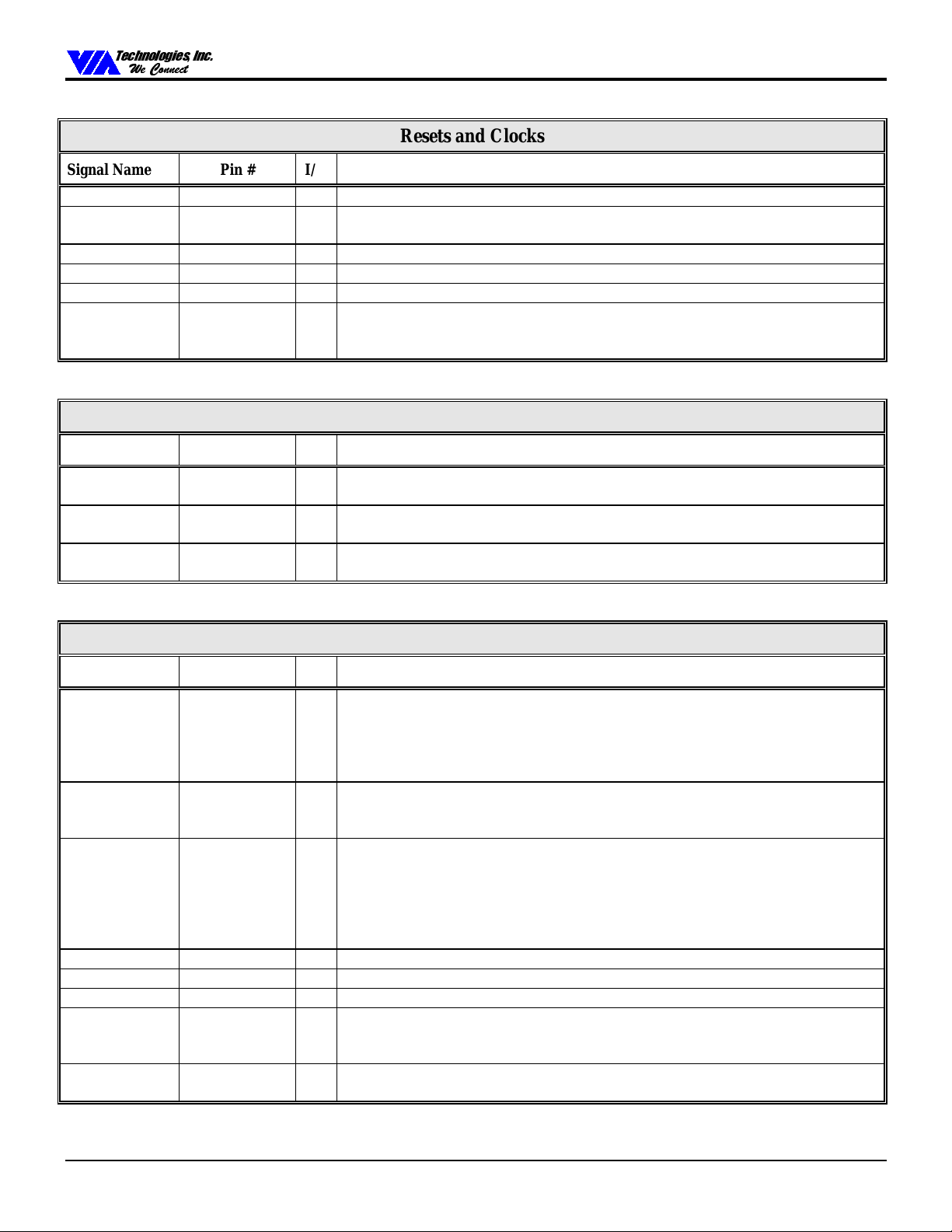
Resets and Clocks
Signal Name Pin # I/O Signal Description
VT82C596B
PWRGD
PCIRST#
RSTDRV
BCLK
OSC
SUSCLK
M18 I
A1 O
W1 O
T7 O
V11 I
P17 O
Power Good.
PCI Reset.
this pin during power-up or from the control register.
Reset Drive.
Bus Clock.
Oscillator.
Suspend Clock.
VT82C598 Apollo MVP3) for DRAM refresh purposes. Stopped during Suspend-to-
Disk and Soft-Off modes.
Connected to the PWRGOOD signal on the Power Supply.
Active low reset signal for the PCI bus. The VT82C596B will assert
Reset signal to the ISA bus.
ISA bus clock.
14.31818 MHz clock signal used by the internal Timer.
32.768 KHz output clock for use by the North Bridge (e.g.,
Configuration and Test
Signal Name Pin # I/O Signal Description
CFG1
CFG2
TEST#
R17 I
R18 I
V18 I
Configuration 1.
the polarity of the INIT and CPURST signals.
Configuration 2.
memory (FFFF0000h-FFFFFFFFh): 0 = Positive decode, 1 = Subtractive decode.
Used to select chip test modes. Pulled up externally to VCCSUS for normal
Test.
operation.
Used to select the CPU type (0=Socket-7, 1=Slot-1). Determines
Used to select the type of decoding for the top 64 Kbytes of
Power and Ground
Signal Name Pin # I/O Signal Description
VCC
VREF
VCCSUS
VBAT
VCCUSB
GNDUSB
GND
NC
E9, E11, E12,
E16, F5, F6,
F14, F15, G6,
P15, R6, R7 ,
R15, T6
J16 P
N16, R16 P
L16 P
K5 P
J5 P
D10, E7, E13,
J9-12, K9-12,
L9-12, M9-12
J4, M5, M16,
N3, N18, R5
P
Core Power.
the mechanical switch on the power supply is turned on and the PWRON signal is
conditioned high. This pin should b e connected to the same voltage as the CPU I/O
circuitry.
Voltage Reference.
voltage should be on only when the mechanical switch on the power supply is turned
on and the PWRON signal is conditioned high.
Suspend Power.
is turned off. If the "soft-off" state is not implemented, then this pin can be
connected to VCC. Signals powered by or referenced to this plane are: BATLOW#,
CFG1-2, EXTSMI#, GPI1, GPO8, IRQ8#, LID, RI#, SMBALRT#, SMBCLK,
SMBDATA, PWRBTN#, SUS[A-C]#, SUSCLK, SUSST[1-2]#, TEST#, PWROK,
RSMRST#.
RTC Battery.
USB Differential Output Power Source
USB Differential Output Ground
P
Ground
-
No Connect
3.3V nominal (3.15V to 3.45V). This supply is turned on only when
Always available unless the mechanical switch of the power supply
Battery input for internal RTC (RTCX1, RTCX2)
5V nominal (4.75 to 5.25) to provide 5V input tolerance. This
(USBP0+, P0-, P1+, P1-)
Revision 0.3 June 17, 1999 -20- Pinouts
Page 27
7HFKQRORJLHV ,QF
&
:H&RQQHFW
RQQHFW
:H
VT82C596B
R
EGISTERS
Register Overview
The following tables summarize the configuration and I/O
registers of the VT82C596B. These tables also document the
power-on default value (“Default”) and access type (“Acc”) for
each register. Access type definitions used are RW
(Read/Write), RO (Read/Only), “—” for reserved / used
(essentially the same as RO), and RWC (or just WC) (Read /
Write 1’s to Clear individual bits). Registers indicated as RW
may have some read/only bits that always read back a fixed
value (usually 0 if unused); registers designated as RWC or
WC may have some read-only or read write bits (see individual
register descriptions for details).
Detailed register descriptions are provided in the following
section of this document. All offset and default values are
shown in hexadecimal unless otherwise indicat ed
Table 2. System I/O Map
Port Function Actual Port Decoding
00-1F Master DMA Controller 0000 0000 000x nnnn
20-3F Master Interrupt Controller 0000 0000 001x xxxn
40-5F Timer / Counter 0000 0000 010x xxnn
60-6F Keyboard Controller 0000 0000 0110 xnxn
(60h) KBC Data 0000 0000 0110 x0x0
(61h) Misc Functions & Spkr Ctrl 0000 0000 0110 xxx1
(64h) KBC Command / Status 0000 0000 0110 x1x0
70-77 RTC/CMOS/NMI-Disable 0000 0000 0111 0nnn
78-7F -available for system use- 0000 0000 0111 1xxx
80 -reserved- (debug port) 0000 0000 1000 0000
81-8F DMA Page Registers 0000 0000 1000 nnnn
90-91 -available for system use- 0000 0000 1001 000x
92 System Control 0000 0000 1001 0010
93-9F -available for system use- 0000 0000 1001 nnnn
A0-BF Slave Interrupt Controller 0000 0000 101x xxxn
C0-DF Slave DMA Controller 0000 0000 110n nnnx
E0-FF -available for system use- 0000 0000 111x xxxx
100-CF7 -available for system useCF8-CFB PCI Configuration Address 0000 1100 1111 10xx
CFC-CFF PCI Configuration Data 0000 1100 1111 11xx
D00-FFFF -available for system use-
Table 3. Registers
Legacy I/O Registers
Port Master DMA Controller Registers Default Acc
00 Channel 0 Base & Current Address RW
01 Channel 0 Base & Current Count RW
02 Channel 1 Base & Current Address RW
03 Channel 1 Base & Current Count RW
04 Channel 2 Base & Current Address RW
05 Channel 2 Base & Current Count RW
06 Channel 3 Base & Current Address RW
07 Channel 3 Base & Current Count RW
08 Status / Command RW
09 Write Request
0A Write Single Mask
0B Write Mode
0C Clear Byte Pointer FF
0D Master Clear
0E Clear Mask
0F Read / Write Mask RW
Port Master Interrupt Controller Regs Default Acc
20 Master Interrupt Control — *
21 Master Interrupt Mask — *
20 Master Interrupt Control Shadow —
21 Master Interrupt Mask Shadow —
* RW if shadow registers are disabled
Timer/Counter Registers Default Acc
Port
40 Timer / Counter 0 Count RW
41 Timer / Counter 1 Count RW
42 Timer / Counter 2 Count RW
43 Timer / Counter Control
Port Keyboard Controller Registers Default Acc
60 Keyboard Controller Data RW
61 Misc Functions & Speaker Control RW
64 Keyboard Ctrlr Command / Status RW
Port CMOS / RTC / NMI Registers Default Acc
70 CMOS Memory Address & NMI Disa
71 CMOS Memory Data (128 bytes) RW
72 CMOS Memory Address RW
73 CMOS Memory Data (256 bytes) RW
74 CMOS Memory Address RW
75 CMOS Memory Data (256 bytes) RW
NMI Disable is port 70h (CMOS Memory Address) bit-7.
RTC control occurs via specific CMOS data locations (0-0Dh).
Ports 72-73 may be used to access all 256 locations of CMOS.
Ports 74-75 may be used to access CMOS if the internal RTC is
disabled.
WO
WO
WO
WO
WO
WO
RW
RW
WO
WO
Revision 0.3 June 17, 1999 -21- Register Overview
Page 28
7HFKQRORJLHV ,QF
&
:H&RQQHFW
RQQHFW
:H
VT82C596B
Port DMA Page Registers Default Acc
87 DMA Page - DM A Channel 0 RW
83 DMA Page - DM A Channel 1 RW
81 DMA Page - DM A Channel 2 RW
82 DMA Page - DM A Channel 3 RW
8F DMA Page - DMA Channel 4 RW
8B DMA Page - DMA Cha nnel 5 RW
89 DMA Page - DM A Channel 6 RW
8A DMA Page - DMA Channel 7 RW
Port System Control Registers Default Acc
92 System Control RW
Port Slave Interrupt Controller Regs Default Acc
A0 Slave Interrupt Control — *
A1 Slave Interrupt Mask — *
A0 Slave Interrupt Control Shadow —
A1 Slave Interrupt Mask Shadow —
* RW accessible if shadow registers are disabled
RW
RW
Slave DMA Controller Registers Default Acc
Port
C0 Channel 0 Base & Current Address RW
C2 Channel 0 Base & Current Count RW
C4 Channel 1 Base & Current Address RW
C6 Channel 1 Base & Current Count RW
C8 Channel 2 Base & Current Address RW
CA Channel 2 Base & Current Count RW
CC Channel 3 Base & Current Address RW
CE Channel 3 Base & Current Count RW
D0 Status / Command RW
D2 Write Request
D4 Write Single Mask
D6 Write Mode
D8 Clear Byte Pointer FF
DA Master Clear
DC Clear Mask
DE Read / Write Mask RW
WO
WO
WO
WO
WO
WO
Revision 0.3 June 17, 1999 -22- Register Overview
Page 29
7HFKQRORJLHV ,QF
&
:H&RQQHFW
RQQHFW
:H
PCI Function 0 Registers - PCI-to-ISA Bridge
VT82C596B
Configuration Space PCI-to-ISA Bridg e Header Registers
Offset PCI Configuration Space Header Default Acc
1-0 Vendor ID 1106 RO
3-2 Device ID 0596 RO
5-4 Command 0087
7-6 Status 0200
8 Revision ID nn RO
9 Programming Interface 00 RO
A Sub Class Code 01 RO
B Base Class Code 06 RO
C -reserved- (cache line size) 00 —
D -reserved- (latency timer) 00 —
E Header Type 80 RO
F Built In Self Test (BIST) 00 RO
10-27 -reserved- (base address registers) 00 —
28-2B -reserved- (unassigned) 00 —
2F-2C Subsystem ID Read 00 RO
30-33 -reserved- (expan. ROM base addr) 00 —
34-3B -reserved- (unassigned) 00 —
3C -reserved- (interrupt line) 00 —
3D -reserved- (interrupt pin) 00 —
3E -reserved- (min gnt) 00 —
3F -reserved- (max lat) 00 —
Configuration Space PCI-to-ISA Bridg e - Specific Registers
RW
WC
Configuration Space PCI-to-ISA Bridg e - Specific Registers
Offset Plug and Play Control Default Acc
50 -reserved- (do not program) 24 RW
51-53 -reserved- 00 —
54 PCI IRQ Edge / Level Selection 00 RW
55 PnP Routing for External MIRQ0-1 00 RW
56 PnP Routing for PCI INTB-A 00 RW
57 PnP Routing for PCI INTD-C 00 RW
58 PnP Routing for External MIRQ2 00 RW
59 PIRQ Pin Configuration 04 RW
5A KBC / RTC Control x4† RW
5B Internal RTC Test Mode 00 RW
5C DMA Control 00 RW
5F-5D -reserved- 00 —
† Bit 7-4 power-up default value depends on external strapping
Distributed DMA Default Acc
Offset
61-60 Channel 0 Base Address / Enable 0000 RW
63-62 Channel 1 Base Address / Enable 0000 RW
65-64 Channel 2 Base Address / Enable 0000 RW
67-66 Channel 3 Base Address / Enable 0000 RW
69-68 Serial IRQ Control 0000 RW
6B-6A Channel 5 Base Address / Enable 0000 RW
6D-6C Channel 6 Base Address / Enable 0000 RW
6F-6E Channel 7 Base Address / Enable 0000 RW
Offset ISA Bus Control Default Acc
40 ISA Bus Control 00 RW
41 ISA Test Mode 00 RW
42 ISA Clock Control 00 RW
43 ROM Decode Control 00 RW
44 Keyboard Controller Control 00 RW
45 Type F DMA Control 00 RW
46 Miscellaneous Control 1 00 RW
47 Miscellaneous Control 2 00 RW
48 Miscellaneous Control 3 01 RW
49 -reserved- 00 —
4A IDE Interrupt Routing 04 RW
4B -reserved- 00 —
4C DMA / Master Mem Access Control 1 00 RW
4D DMA / Master Mem Access Control 2 00 RW
4F-4E DMA / Master Mem Access Control 3 0300 RW
Offset Miscellaneous Default Acc
70 Subsystem ID Write 00 WO
71-73 -reserved- 00 —
77-74 GPIO / Chip Select Control 0000 0000 RW
7B-78 Programmable Chip Select Control 0000 0000 RW
7F-7C PC/PCI Control 0000 0000 RW
80 Programmable Chip Select Mask 00 RW
81 ISA Positive Decoding Control 1 00 RW
82 ISA Positive Decoding Control 2 00 RW
83 ISA Positive Decoding Control 3 00 RW
84 ISA Positive Decoding Control 4 00 RW
85-86 -reserved- 00 —
87 Test 1 00 RW
88 Test 2 00 RW
89 PLL Control 00 RW
8A-FF -reserved- 00 —
Revision 0.3 June 17, 1999 -23- Register Overview
Page 30
7HFKQRORJLHV ,QF
&
:H&RQQHFW
RQQHFW
:H
PCI Function 1 Registers – IDE Controller
VT82C596B
Configuration Space IDE Header Registers
Offset PCI Configuration Space Header Default Acc
1-0 Vendor ID 1106 RO
3-2 Device ID 0571 RO
5-4 Command 0080 RO
7-6 Status 0280
8 Revision ID nn RO
9 Programming Interface 85
A Sub Class Code 01 RO
B Base Class Code 01 RO
C -reserved- (cache line size) 00 —
D Latency Timer 00 RW
E Header Type 00 RO
F Built In Self Test (BIST) 00 RO
13-10 Base Address – Pri Data / Command 000001F0 RO
17-14 Base Address – Pri Control / Status 000003F4 RO
1B-18 Base Address – Sec Data / Command 00000170 RO
1F-1C Base Address – Sec Control / Status 00000374 RO
23-20 Base Address – Bus Master Control 0000CC01
24-2F -reserved- (unassigned) 00 —
30-33 -reserved- (expan ROM base addr) 00 —
34-3B -reserved- (unassigned) 00 —
3C Interrupt Line 0E RW
3D Interrupt Pin 00 RO
3E Mi nimum Grant 00 RO
3F Maximum Latency 00 RO
RW
RW
RW
Configuration Space IDE-Specific Registers
Offset Configuration Space IDE Registers Default Acc
40 Chip Enable 08 RW
41 IDE Configuration 02 RW
42 -reserved- (do not program) 09
43 FIFO Co nfiguration 3A RW
44 Miscellaneous Control 1 68 RW
45 Miscellaneous Control 2 00 RW
46 Miscellaneous Control 3 C0 RW
4B-48 Drive Timing Control
4C Address Setup Time FF RW
4D -reserved- (do not program) 00
4E Sec Non-1F0 Port Access Timing FF RW
4F Pri Non-1F0 Port Access Timing FF RW
53-50 UltraDMA33 Extd Timing Control 03030303 RW
54 UltraDMA FIFO Control 06 RW
55-5F -reserved- 00 —
61-60 IDE Primary Sector Size 0200 RW
62-67 -reserved- 00 —
69-68 IDE Secondary Sector Size 0200 RW
69-6F -reserved- 00 —
70 IDE Primary Status 00 RW
71 IDE Primary Interrupt Control 00 RW
72-73 -reserved- 00 —
74 IDE Primary Comma nd 1 00 RW
75 IDE Primary Comma nd 2 00 RW
76-77 -reserved- 00 —
78 IDE Secondary Status 00 RW
79 IDE Secondary Interrupt Control 00 RW
7A-7B -reserved- 00 —
7C IDE Secondary Command 1 00 RW
7D IDE Secondary Command 2 00 RW
7E-7F -reserved- 00 —
83-80 IDE Primary S/G Descriptor Address 0000 0000 RW
84-87 -reserved- 00 —
8B-88 IDE Secondary S/G Descriptor Addr 0000 0000 RW
8C-FF -reserved- 00 —
A8A8A8A8
RW
RW
RW
I/O Registers – IDE Controller (SFF 8038 v1.0 Compliant
Offset IDE I/O Registers Default Acc
0 Primary Channel Command 00 RW
1 -reserved- 00 —
2 Primary Channel Status 00 WC
3 -reserved- 00 —
4-7 Primary Channel PRD Table Addr 00 RW
8 Se condary Channel Command 00 RW
9 -reserved- 00 —
A Secondary Channel Status 00 WC
B -reserved- 00 —
C-F Secondary Channel PRD Table Addr 00 RW
Revision 0.3 June 17, 1999 -24- Register Overview
Page 31

7HFKQRORJLHV ,QF
&
:H&RQQHFW
RQQHFW
:H
PCI Function 2 Registers – USB Controller
VT82C596B
Configuration Space USB Header Registers
Offset PCI Configuration Space Header Default Acc
1-0 Vendor ID 1106 RO
3-2 Device ID 3038 RO
5-4 Command 0000
7-6 Status 0200
8 Revision ID nn RO
9 Programming Interface 00 RO
A Sub Class Code 03 RO
B Base Class Code 0C RO
C Cache Line Size 00 RO
D Latency Timer 16
E Header Type 00 RO
FBIST 00 RO
10-1F -reserved- 00 —
23-20 Base Address 00000301
24-3B -reserved- 00 —
3C Interrupt Line 00
3D Interrupt Pin 04
3E-3F -reserved- 00 —
Configuration Space USB-Specific Registers
Offset USB Control Default Acc
40 Miscellaneous Control 1 00
41 Miscellaneous Control 2 00
42-43 -reserved- 00 RO
44-45 -reserved- (test only, do not program)
46-47 -reserved- (test) RO
48-5F -reserved- 00 —
60 Serial Bus Release Number 10 RO
61-BF -reserved- 00 —
C1-C0 Legacy Support 2000
C2-FF -reserved- 00 —
RW
WC
RW
RW
RW
RO
RW
RW
RW
RW
I/O Registers – USB Controller
Offset USB I/O Registers Default Acc
1-0 USB Command 0000 RW
3-2 USB Status 0000
5-4 USB Interrupt Enable 0000 RW
7-6 Frame Number 0000 RW
B-8 Frame List Base Address 00000000 RW
C Start Of Frame Modify 40 RW
11-10 Port 1 Status / Control 0080
13-12 Port 2 Status / Control 0080
WC
WC
WC
Revision 0.3 June 17, 1999 -25- Register Overview
Page 32

7HFKQRORJLHV ,QF
&
:H&RQQHFW
RQQHFW
:H
PCI Function 3 Registers – Power Management
VT82C596B
Configuration Space Power Management Header Registers
Offset PCI Configuration Space Header Default Acc
1-0 Vendor ID 1106 RO
3-2 Device ID 3050 RO
5-4 Command 0000 RO
7-6 Status 0280
8 Revision ID nn RO
9Programming Interface
A Sub Class Code
B Base Class Code
C Cache Line Size 00 RO
D Latency Timer 00 RO
E Header Type00RO
FBIST 00 RO
10-3F -reserved- 00 —
† Default values may be changed by writing to offsets 61-63h.
WC
RO
RO
RO
Configuration Space Power Management-Specific Registers
Offset Power Management Default Acc
40 Debounce Control 00 RW
41 General Configuration 00 RW
42 SCI Interrupt Configuration 00 RW
43 -reserved- 00 —
45-44 Primary Interrupt Channel 0000 RW
47-46 Secondary Interrupt Channel 0000 RW
4B-48 Power Mgmt I/O Base (256 Bytes) 0000 0001 RW
4C Host Bus Power Management Control 00 RW
4D Clock Stop Control 00 RW
4E-4F -reserved- 00
53-50 GP0/1 Timer Control 0000 0000 RW
54 GPIO Select 00 RW
55 Wakeup Control 00 RW
56-57 -reserved- 00
5B-58 GP2/3 Timer Control 0000 0000 RW
5C-60 -reserved- 00
61 Write value for Offset 9 (Prog Intfc) 00
62 Write value for Offset A (Sub Class) 00
63 Write value for Offset B (Base Class) 00
64-8F -reserved- 00
Offset System Management Bus Default Acc
93-90 SMBus I/O Base 0000 0001 RW
94-D1 -reserved- 00
D2 SMBus Control 00 RW
D3 SMBus Host Slave Command 00 RW
D4 SMBus Slave Address for Port 1 00 RW
D5 SMBus Slave Address for Port 2 00 RW
D6 SMBus Revision ID nn
D7-FF -reserved- 00
—
—
—
WO
WO
WO
—
—
RO
—
Revision 0.3 June 17, 1999 -26- Register Overview
Page 33

7HFKQRORJLHV ,QF
&
:H&RQQHFW
RQQHFW
:H
VT82C596B
I/O Space System Management Bus Registers
Offset System Management Bus Default Acc
0 SMBus Host Status 00
1 SMBus Slave Status 00 RW
2 SMBus Host Control 00 RW
3 SMBus Host Command 00 RW
4 SMBus Host Address 00 RW
5 SMBus Host Data 0 00 RW
6 SMBus Host Data 1 00 RW
7 SMBus Block Data 00 RW
8 SMBus Slave Control 00 RW
9 SMBus Shadow Command 00
A-B SMBus Slave Event 0000 RW
C-D SMBus Slave Data 0000
E-F -reserved- 00
WC
RO
RO
—
I/O Space Power Management- Registers
Offset Basic Control / Status Registers Default Acc
1-0 Power Management Status 0000
3-2 Power Management Enable 0000 RW
5-4 Power Management Control 0000 RW
6-7 -reserved- 00
B-8 Power Management Timer 0000 0000 RW
C-F -reserved- 00
Offset Processor Registers Default Acc
13-10 Processor and PCI Bus Control 0000 0000 RW
14 Processor LVL2 00
15 Processor LVL3 00
16-1F -reserved- 00
Offset General Purpose Registers Default Acc
21-20 General Purpose Status 0000
23-22 General Purpose SCI Enable 0000 RW
25-24 General Purpose SMI Enable 0000 RW
26-27 -reserved- 00
Offset Generic Registers Default Acc
29-28 Global Status 0000
2B-2A Global Enable 0000 RW
2D-2C Global Control 0010 RW
2E -reserved- 00
2F SMI Command 00 RW
33-30 Primary Activity Detect Status 0000 0000
37-34 Primary Activity Detect Enable 0000 0000 RW
3B-38 GP Timer Reload Enable 0000 0000 RW
3C-3F -reserved- 00
Offset General Purpose I/O Registers Default Acc
40 General Purpose Control 00 RW
41-43 -reserved- 00
45-44 External SMI Input Value input
46-47 -reserved- 00
4B-48 GPI Port Input Value input
4F-4C GPO Port Output Value 7FFFFFFF RW
50-FF -reserved- 00
WC
—
—
RO
RO
—
WC
—
WC
—
WC
—
—
RO
—
RO
—
Revision 0.3 June 17, 1999 -27- Register Overview
Page 34

7HFKQRORJLHV ,QF
&
:H&RQQHFW
RQQHFW
:H
Configuration Space I/O
Mechanism #1
These ports respond only to double-word accesses. Byte or
word accesses will be passed on unchanged.
Port CFB-CF8 - Configuration Address ......................... RW
31 Configuration Space Enable
0 Disabled .................................................default
1 Convert configuration data port writes to
configuration cycles on the PCI bus
30-24 Reserved
23-16 PCI Bus Number
Used to choose a specific PCI bus in the system
15-11 Device Number
Used to choose a specific device in the system
10-8 Function Number
Used to choose a specific function if the selected
device supports multiple functions
7-2 Register Number
Used to select a specific DWORD in the device’s
configuration space
1-0 Fixed
........................................ always reads 0
........................................ always reads 0
VT82C596B
Port CFF-CFC - Configuration Data .............................. RW
Refer to PCI Bus Specification Version 2.1 for further details
on operation o f the above configuration registe rs.
Revision 0.3 June 17, 1999 -28- Configuration Space I/O
Page 35

7HFKQRORJLHV ,QF
&
:H&RQQHFW
RQQHFW
:H
VT82C596B
Register Descriptions
Legacy I/O Ports
This group of registers includes the DMA Controllers,
Interrupt Controllers, and Timer/Counters as well as a number
of miscellaneous ports originally implemented using discrete
logic on original PC/AT motherboards. All of the registers
listed are integrated on-chip. These registers are implemented
in a precise manner for backwards compatibility with previous
generations of PC hardware. These registers are listed for
information purposes only. Detailed descriptions of the
actions and programming of these registers are included in
numerous industry publications (duplication of that
information here is beyond the scope of this document). All of
these registers reside in I/O space.
Port 61 - Misc Functions & Speaker Control ................. RW
7 Reserved
6 IOCHCK# Active
This bit is set when the ISA bus IOCHCK# signal is
asserted. Once set, this bit may be cleared by setting
bit-3 of this register. Bit-3 should be cleared to
enable recording of the next IOCHCK#. IOCHCK#
generates NMI to the CPU if NMI is enabled.
5 Timer/Counter 2 Output
This bit reflects the output of Timer/Counter 2
without any synchronization.
4 Refresh Detected
This bit toggles on every rising edge of the ISA bus
REFRESH# signal.
3 IOCHCK# Disable
0 Enable IOCHCK# assertions..................default
1 Force IOCHCK# inactive and clear any
2 Reserved
1 Speaker Enable
0 Disable ...................................................default
1 Enable Timer/Ctr 2 output to drive SPKR pin
0 Timer/Counter 2 Enable
0 Disable ...................................................default
1 Enable Timer/Counter 2
........................................ always reads 0
.................................................RO
.....................................RO
..................................................RO
..............................................RW
“IOCHCK# Active” condition in bit-6
........................................RW, default=0
....................................................RW
.....................................RW
Port 92h - System Control ................................................ RW
7-6 Hard Disk Activity LED Status
0 Off ....................................................default
1-3 On
5-4 Reserved
3 Power-On Password Bytes Inaccessable
2 Reserved
1 A20 Address Line Enable
0 A20 disabled / forced 0 (real mode) ...... default
1 A20 address line enabled
0 High Speed Reset
0Normal
1 Briefly pulse system reset to switch from
........................................always reads 0
..default=0
........................................always reads 0
protected mode to real mode
Revision 0.3 June 17, 1999 -29- Register Descriptions - Legacy I/O Ports
Page 36

7HFKQRORJLHV ,QF
&
:H&RQQHFW
RQQHFW
:H
VT82C596B
Keyboard Controller Registers
The keyboard controller handles the keyboard and mouse
interfaces. Two ports are used: port 60 and port 64. Reads
from port 64 return a status byte. Writes to port 64h are
command codes (see command code list following the register
descriptions). Input and output data is transferred via port 60.
A “Control” register is also available. It is accessable by
writing commands 20h / 60h to the command port (port 64h);
The control byte is written by first sending 60h to the
command port, then sending the control byte value. The
control register may be read by sending a command of 20h to
port 64h, waiting for “Output Buffer Full” status = 1, then
reading the control byte value from port 60h.
Traditional (non-integrated) keyboard controllers have an
“Input Port” and an “Output Port” with specific pins dedicated
to certain functions and other pins available for general
purpose I/O. Specific commands are provided to set these pins
high and low. All outputs are “open-collector” so to allow
input on one of these pins, the output value for that pin would
be set high (non-driving) and the desired input value read on
the input port. These ports are defined as follows:
Bit Input Port
0 P10 - Keyboard Data In B0 B8
1 P11 - Mouse Data In B1 B9
2 P12 - Turbo Pin (PS/2 mode only) B2 BA
3 P13 - user-defined B3 BB
4 P14 - user-defined B6 BE
5 P15 - user-defined B7 BF
6 P16 - user-defined – –
7 P17 - undefined – –
Bit Output Port
0 P20 - SYSRST (1=execute reset) – –
1 P21 - GATEA20 (1=A20 enabled) – –
2 P22 - Mouse Data Out B4 BC
3 P23 - Mouse Clock Out B5 BD
4 P24 - Keyboard OBF Interrupt (IRQ1) – –
5 P25 - Mouse OBF Interrupt (IRQ 12) – –
6 P26 - Keyboard Clock Out – –
7 P27 - Keyboard Data Out – –
Bit Test Port Lo Code
0 T0 - Keyboard Clock In – –
1 T1 - Mouse Clock In – –
Note: Command code C0h transfers input port data to the
output buffer. Command code D0h copies output port values
to the output buffer. Command code E0h transfers test input
port data to the output buffer.
Port 60 - Keyboard Controller Input Buffer ................. WO
Only write to port 60h if port 64h bit-1 = 0 (1=full).
Port 60 - Keyboard Controller Output Buffer ................ RO
Only read from port 60h if port 64h bit-0 = 1 (0=empty).
Lo Code Hi Code
Lo Code Hi Code
Hi Code
Port 64 - Keyboard / Mouse Status .................................. RO
0 Keyboard Output Buff er Full
0 Keyboard Output Buffer Empty.............default
1 Keyboard Output Buffer Full
1 Input Buffer Full
0 Input Buffer Empty................................ default
1 Input Buffer Full
2 System Flag
0 Power-On Default..................................default
1 Self T e st Successful
3 Command / Data
0 Last write was data write ....................... default
1 Last write was command write
4 Keylock Status
0Locked
1Free
5 Mouse Output Buffer Full
0 Mouse output buffer empty....................default
1 Mouse output buffer holds mouse data
6 General Receive / Transmit Timeout
0 No error .................................................default
1 Error
7 Parity Error
0 No parity error (odd parity received).....default
1 Even parity occurred on last byte received
from keyboard / mouse
KBC Control Register .......... (R/W via Commands 20h/60h)
7 Reserved
6 PC Compatibility
0 Disable scan conversion
1 Convert scan codes to PC format; convert 2-
5 Mouse Disable
0 Enable Mouse Interface.........................default
1 Disable Mouse Interface
4 Keyboard Disable
0 Enable Keyboard Interface .................... default
1 Disable Keyboard Interface
3 Keyboard Lock Disable
0 Enable Keyboard Inhibit Function......... default
1 Disable Keyboard Inhibit Function
2 System Flag
This bit may be read back as status register bit-2
1 Mouse Interrupt Enable
0 Disable mouse interrupts .......................default
1 Generate interrupt on IRQ12 when mouse data
0 Keyboard Interrupt Enable
0 Disable Keyboard Interrupts..................default
1 Generate interrupt on IRQ1 when output buffer
........................................always reads 0
byte break sequences to 1-byte PC-compatible
break codes............................................ default
................................................default=0
comes in output bufer
has been written.
Revision 0.3 June 17, 1999 -30- Register Descriptions - Legacy I/O Ports
Page 37

7HFKQRORJLHV ,QF
&
:H&RQQHFW
RQQHFW
:H
Port 64 - Keyboard / Mouse Command .......................... WO
This port is used to send co mmands to the keyboard / mouse
controller. The command codes recognized by the
VT82C596B are listed n the table below.
Note: The VT82C596B Keyboard Controller is compatible
with the VIA VT82C42 Industry-Standard Keyboard
Controller except that due to its integrated nature, many of the
input and output port pins are not available externally for use
as general purpo se I/O pins (even though P 13-P16 are set on
power-up as strapping options). In other words, many of the
commands below are provided and “work”, but otherwise
perform no useful function (e. g., commands that set P12-P 17
high or low). Also note that setting P10-11, P22-23, P26-27,
and T0-1 high or lo w directly serves no useful purpose, sinc e
these bits are used to implement the keyboard and mouse ports
and are directly controlled by keyboard controller logic.
Table 4. Keyboard Controller Command Codes
VT82C596B
Code Key board Command Code Description
20h Read Control Byte (next byte is Control Byte)
21-3Fh Read SRAM Data (next byte is Data Byte)
60h Write Control Byte (next byte is Control Byte)
61-7Fh Write SRAM Data (next byte is Data Byte)
9xh Write low nibble (bits 0-3) to P10-P13
A1h Output Keyboard Controller Version #
A4h Test if Password is installed
(always returns F1h to indicate not installed)
A7h Disable Mouse Interface
A8h Enable Mouse Interface
A9h Mouse Interface Test (puts test results in port 60h)
(value: 0=OK, 1=clk stuck low, 2=clk stuck high,
3=data stuck lo, 4= data stuck hi, FF=general error)
AAh KBC self test (returns 55h if OK, FCh if not)
ABh Keyboard Interface Test (see A9h Mouse Test)
ADh Disable Keyboard Interface
AEh Enable Keyboard Interface
AFh Return Version #
B0h Set P10 low
B1h Set P11 low
B2h Set P12 low
B3h Set P13 low
B4h Set P22 low
B5h Set P23 low
B6h Set P14 low
B7h Set P15 low
B8h Set P10 high
B9h Set P11 high
BAh Set P12 high
BBh Set P13 high
BCh Set P22 high
BDh Set P23 high
BEh Set P14 high
BFh Set P15 high
Code Key board Command Code Description
C0h Read input port (read P10-17 input data to
the output buffer)
C1h Poll input port low (read input data on P11-13
repeatably & put in bits 5-7 of status
C2h Poll input port high (same except P15-17)
C8h Unblock P22-23 (use before D1 to change
active mode)
C9h Reblock P22-23 (protection mechanism for D1)
CAh Read mode (output KBC mode info to port 60
output buffer (bit-0=0 if ISA, 1 if PS/2)
D0h Read Output Port (copy P10-17 output port values
to port 60)
D1h Write Output Port (data byte following is written to
keyboard output port as if it came from keyboard)
D2h Write Keyboard Output Buffer & clear status bit-5
(write following byte to keyboard)
D3h Write Mouse Output Buffer & set status bit-5 (write
following byte to mouse; put value in mouse input
buffer so it appears to have come from the mouse)
D4h Write Mouse (write following byte to mouse)
E0h Read test inputs (T0-1 read to bits 0-1 of resp byte)
Exh Set P23-P21 per command bits 3-1
Fxh Pulse P23-P20 low for 6usec per command bits 3-0
All other codes not listed are undefined.
Revision 0.3 June 17, 1999 -31- Register Descriptions - Legacy I/O Ports
Page 38

7HFKQRORJLHV ,QF
&
:H&RQQHFW
RQQHFW
:H
VT82C596B
DMA Controller I/O Registers
Ports 00-0F - Master DMA Controller
Channels 0-3 of the Master DMA Controller control System
DMA Channels 0-3. There are 16 Master DMA Controller
registers:
I/O Address Bits 15-0 Register Name
0000 0000 000x 0000 Ch 0 Base / Current Address RW
0000 0000 000x 0001 Ch 0 Base / Current Count RW
0000 0000 000x 0010 Ch 1 Base / Current Address RW
0000 0000 000x 0011 Ch 1 Base / Current Count RW
0000 0000 000x 0100 Ch 2 Base / Current Address RW
0000 0000 000x 0101 Ch 2 Base / Current Count RW
0000 0000 000x 0110 Ch 3 Base / Current Address RW
0000 0000 000x 0111 Ch 3 Base / Current Count RW
0000 0000 000x 1000 Status / Command RW
0000 0000 000x 1001 Write Request WO
0000 0000 000x 1010 Write Single Mask WO
0000 0000 000x 1011 Write Mode WO
0000 0000 000x 1100 Clear Byte Pointer F/F WO
0000 0000 000x 1101 Master Clear WO
0000 0000 000x 1110 Clear Mask WO
0000 0000 000x 1111 R/W All Mask Bits RW
Note that not all bits of the address are decoded.
The Master DMA Controller is compatible with the Intel 8237
DMA Controller chip. Detailed descriptions of 8237 DMA
Controller operation can be obtained from the Intel Peripheral
Components Data Book and numerous other industry
publications.
Ports C0-DF - Slave DMA Controller
Channels 0-3 of the Slave DMA Controller control System
DMA Channels 4-7. There are 16 Slave DMA Controller
registers:
I/O Address Bits 15-0 Register Name
0000 0000 1100 000x Ch 0 Base / Current Address RW
0000 0000 1100 001x Ch 0 Base / Current Count RW
0000 0000 1100 010x Ch 1 Base / Current Address RW
0000 0000 1100 011x Ch 1 Base / Current Count RW
0000 0000 1100 100x Ch 2 Base / Current Address RW
0000 0000 1100 101x Ch 2 Base / Current Count RW
0000 0000 1100 110x Ch 3 Base / Current Address RW
0000 0000 1100 111x Ch 3 Base / Current Count RW
0000 0000 1101 000x Status / Command RW
0000 0000 1101 001x Write Request WO
0000 0000 1101 010x Write Single Mask WO
0000 0000 1101 011x Write Mode WO
0000 0000 1101 100x Clear Byte Pointer F/F WO
0000 0000 1101 101x Master Clear WO
0000 0000 1101 110x Clear Mask WO
0000 0000 1101 111x Read/Write All Mask Bits WO
Note that not all bits of the address are decoded.
The Slave DMA Controller is compatible with the Intel 8237
DMA Controller chip. Detailed description of 8237 DMA
controller operation can be obtained from the Intel Peripheral
Components Data Book and numerous other industry
publications.
Ports 80-8F - DMA Page Registers
There are eight DMA Page Registers, one for each DMA
channel. These registers provide bits 16-23 of the 24-bit
address for each DMA channel (bits 0-15 are stored in
registers in the Master and Slave DMA Controllers). They are
located at the following I/O Port addresses:
I/O Address Bits 15-0 Register Name
0000 0000 1000 0111 Channel 0 DMA Page (M-0).........RW
0000 0000 1000 0011 Channel 1 DMA Page (M-1).........RW
0000 0000 1000 0001 Channel 2 DMA Page (M-2).........RW
0000 0000 1000 0010 Channel 3 DMA Page (M-3).........RW
0000 0000 1000 1111 Channel 4 DMA Page (S-0)..........RW
0000 0000 1000 1011 Channel 5 DMA Page (S-1)..........RW
0000 0000 1000 1001 Channel 6 DMA Page (S-2)..........RW
0000 0000 1000 1010 Channel 7 DMA Page (S-3) .........RW
Revision 0.3 June 17, 1999 -32- Register Descriptions - Legacy I/O Ports
Page 39

7HFKQRORJLHV ,QF
&
:H&RQQHFW
RQQHFW
:H
VT82C596B
Interrupt Controller Registers
Ports 20-21 - Master Interrupt Controller
The Master Interrupt Controller controls system interrupt
channels 0-7. Two registers control the Master Interrupt
Controller. They are:
I/O Address Bits 15-0 Register Name
0000 0000 001x xxx0 Master Interrupt Control RW
0000 0000 001x xxx1 Master Interrupt Mask RW
Note that not all bits of the address are decoded.
The Master Interrupt Controller is compatible with the Intel
8259 Interrupt Controller chip. Detailed descriptions of 8259
Interrupt Controller operation can be obtained from the Intel
Peripheral Components Data Book and numerous other
industry publications.
Ports A0-A1 - Slave Interrupt Contro ller
The Slave Interrupt Controller controls system interrupt
channels 8-15. The slave system interrupt controller also
occupies two register locations:
I/O Address Bits 15-0 Register Name
0000 0000 101x xxx0 Slave Interrupt Control RW
0000 0000 101x xxx1 Slave Interrupt Mask RW
Note that not all address bits are decoded.
The Slave Interrupt Controller is compatible with the Intel
8259 Interrupt Controller chip. Detailed descriptions of 8259
Interrupt Controller operation can be obtained from the Intel
Peripheral Components Data Book and numerous other
industry publications.
Interrupt Controller Shadow Registers
The following shadow registers are enabled by setting bit 4 of
Rx47 to 1 (offset 47h in the PCI-ISA Bridge function 0
register group). If the shadow registers are enabled, they are
read back at the indicated I/O port instead of the standard
interrupt controller registers (writes to the interrupt controller
register ports are directed to the standard interrupt controller
registers).
Port 20 - Master Interrupt Control Shadow ................... RO
7-5 Reserved
4OCW3 bit 5
3OCW2 bit 7
2ICW4 bit 4
1ICW4 bit 1
0ICW1 bit 3
Port 21 - Master Interrupt Mask Shadow ....................... RO
7-5 Reserved
4-0 T7-T3 of Interrupt Vector Address
Port A0 - Slave Interrupt Control Shadow ..................... RO
7-5 Reserved
4OCW3 bit 5
3OCW2 bit 7
2ICW4 bit 4
1ICW4 bit 1
0ICW1 bit 3
Port A1 - Slave Interrupt Mask Shadow ........................ RO
7-5 Reserved
4-0 T7-T3 of Interrupt Vector Address
Timer / Counter Registers
........................................always reads 0
........................................always reads 0
........................................always reads 0
........................................always reads 0
Ports 40-43 - Timer / Counter Registers
There are 4 Timer / Counter registers:
I/O Address Bits 15-0 Register Name
0000 0000 010x xx00 Timer / Counter 0 Count RW
0000 0000 010x xx01 Timer / Counter 1 Count RW
0000 0000 010x xx10 Timer / Counter 2 Count RW
0000 0000 010x xx11 Timer / Counter Cm d Mode WO
Note that not all bits of the address are decoded.
The Timer / Counters are compatible with the Intel 8254
Timer / Counter chip. Detailed descriptions of 8254 Timer /
Counter operation can be obtained from the Intel Peripheral
Components Data Book and numerous other industry
publications.
Revision 0.3 June 17, 1999 -33- Register Descriptions - Legacy I/O Ports
Page 40

7HFKQRORJLHV ,QF
&
:H&RQQHFW
RQQHFW
:H
CMOS / RTC Registers
Port 70 - CMOS Address ................................................. WO
7NMI Disable
0 Enable NMI Generation. NMI is asserted on
1 Disable NMI Generation ........................default
6-0 CMOS Address
Port 71 - CMOS Data........................................................ RW
7-0 CMOS Data
Note: P orts 70-71 may be accessed if Rx5A bit-2 is set to
one to select the internal RTC. If Rx5A bit-2 is set to
zero, accesses to ports 70-71 will be directed to an
external RTC.
.........................................................WO
encountering IOCHCK# on the ISA bus or
SERR# on the PCI bus.
(lower 128 bytes).......................WO
(128 bytes)
Offset Description
00 Seconds
01 Seconds Alarm
02 Minutes
03 Minutes Alarm
04 Hours
05 Hours Alarm
06 Day of the Week
07 Day of the Month
08 Month
09 Year
VT82C596B
Binary Range BCD Range
00-3Bh 00-59h
00-3Bh 00-59h
00-3Bh 00-59h
00-3Bh 00-59h
am 12hr: 01-1Ch 01-12h
pm 12hr: 81-8Ch 81-92h
24hr: 00-17h 00-23h
am 12hr: 01-1Ch 01-12h
pm 12hr: 81-8Ch 81-92h
24hr: 00-17h 00-23h
Sun=1: 01-07h 01-07h
01-1Fh 01-31h
01-0Ch 01-12h
00-63h 00-99h
Port 72 - CMOS Address .................................................. RW
7-0 CMOS Address
Port 73 - CMOS Data........................................................ RW
7-0 CMOS Data
Note: P orts 72-73 may be accessed if Rx5A bit-2 is set to
one to select the internal RTC. If Rx5A bit-2 is set to
zero, accesses to ports 72-73 will be directed to an
external RTC.
Port 74 - CMOS Address .................................................. RW
7-0 CMOS Address
Port 75 - CMOS Data........................................................ RW
7-0 CMOS Data
Note: P orts 74-75 may be accessed only if Function 0 Rx5B
bit-1 is set to one to enable the internal RTC SRAM
and if Rx48 bit-3 (Port 74/75 Access Enable) is set to
one to enable port 74/75 access.
Note: Ports 70-71 are compatible with PC industry-
standards and may be used to access the lower 128
bytes of the 256-byte on-chip CMOS RAM. Ports
72-73 may be used to access the full extended 256byte space. Ports 74-75 may be used to access the
full on-chip extended 256-byte space in cases where
the on-chip RTC is disabled.
Note: The system Real Time Clock (RTC) is part of the
“CMOS” block. The RTC control registers are
located at specific offsets in the CMOS data area (00Dh and 7D-7Fh). Detailed descriptions of CMOS /
RTC operation and programming can be obtained
from the VIA VT82887 Data Book or numerous
other industry publications. For reference, the
definition of the RTC register locations and bits are
summarized in the following table:
(256 bytes).................................RW
(256 bytes)
(256 bytes).................................RW
(256 bytes)
0A Register A
7UIP
6-4 DV2-0
3-0 RS3-0
0B Register B
7SET
6PIE
5AIE
4UIE
3SQWE
2DM
1 24/12
0DSE
0C Register C
7IRQF
6PF
5AF
4UF
3-0 0
0D Register D
7 VRT
6-0 0
0E-7C Software-Defined Storage Registers
Offset Extended Functions
7D Date Alarm
7E Month Alarm
7F Century Field
80-FF Software-Defined Storage Registers
(See also Function 0 Rx5B[3] and Rx77[2-1])
Update In Progress
Divide (010=ena osc & keep time)
Rate Select for Periodic Interrupt
Inhibit Update Transfers
Periodic Interrupt Enable
Alarm Interrupt Enable
Update Ended Interrupt Enable
No function (read/write bit)
Data Mode (0=BCD, 1=binary)
Hours Byte Format (0=12, 1=24)
Daylight Savings Enable
Interrupt Request Flag
Periodic Interrupt Flag
Alarm Interrupt Flag
Update Ended Flag
Unused (always read 0)
Reads 1 if VBAT voltage is OK
Unused (always read 0)
Binary Range BCD Range
01-1Fh 01-31h
01-0Ch 01-12h
13-14h 19-20h
Table 5. CMOS Register Summary
(111 Bytes)
(128 Bytes)
Revision 0.3 June 17, 1999 -34- Register Descriptions - Legacy I/O Ports
Page 41

7HFKQRORJLHV ,QF
&
:H&RQQHFW
RQQHFW
:H
Function 0 Registers - PCI to ISA Bridge
All registers are located in the function 0 PCI configuration
space of the VT82C596B. These registers are accessed
through PCI configuration mechanism #1 via I/O address
CF8/CFC.
PCI Configuration Space Header
VT82C596B
Offset 1-0 - Vendor ID = 1106h ......................................... RO
Offset 3-2 - Device ID = 0596h .......................................... RO
Offset 5-4 - Command ....................................................... RW
15-8 Reserved
7 Address / Data Stepping
0 Disable
1 Enable ....................................................default
6-4 Reserved
3 Special Cycle Enable
2Bus Master
1 Memory Space
0 I/O Space
† If the test bit at offset 46 bit-4 is set, access to the above
indicated bits is reversed: bit-3 above becomes read only
(reading back 1) and bits 0-1 above become read / write (with
a default of 1).
Offset 7-6 - Status ........................................................... RWC
15 Detected Parity Error
14 Signalled System Error
13 Signalled Master Abort
12 Received Target Abort
11 Signalled Target Abort
10-9 DEVSEL# Timing
8 Data Parity Detected
7 Fast Back-to-Back Capable
6-0 Reserved
........................................ always reads 0
........................................ always reads 0
.....Normally RW†, default = 0
........................................ always reads 1
.................. Normally RO†, reads as 1
...................... Normally RO†, reads as 1
....................write one to clear
...................... always reads 0
.................write one to clear
..................write one to clear
..................write one to clear
....................fixed at 01 (medium)
.......................... always reads 0
............... always reads 0
........................................ always reads 0
Offset 8 - Revision ID = nn ................................................ RO
7-0 Revision ID (00h is first silicon)
Offset 9 - Program Interface = 00h .................................. RO
Offset A - Sub Class Code = 01h ....................................... RO
Offset B - Class Code = 06h .............................................. RO
Offset E - Header Type = 80h ........................................... RO
7-0 Header Type Code.........
Offset F - BIST = 00h ........................................................ RO
Offset 2F-2C - Subsystem ID ............................................ RO
Use offset 70-73 to change the value returned.
80h (Multifunction Device)
Revision 0.3 June 17, 1999 -35- PCI Function 0 Registers - PCI-to-ISA Bridge
Page 42

7HFKQRORJLHV ,QF
&
:H&RQQHFW
RQQHFW
:H
ISA Bus Control
VT82C596B
Offset 40 - ISA Bus Control .............................................. RW
7 ISA Command Delay
0 Normal ...................................................default
1Extra
6 Extended ISA Bus Ready
0 Disable ...................................................default
1Enable
5 ISA Slave Wait States
0 4 Wait States ..........................................default
1 5 Wait States
4 Chipset I/O Wait States
0 2 Wait States ..........................................default
1 4 Wait States
3 I/O Recovery Time
0 Disable ...................................................default
1Enable
2 Extend-ALE
0 Disable ...................................................default
1Enable
1ROM Wait States
0 1 Wait State............................................default
1 0 Wait States
0 ROM Write
0 Disable ...................................................default
1Enable
Offset 42 - ISA Clock Control. ......................................... RW
7 Latch IO16#
0 Enable (recommended setting) .............. default
1 Disable
6 MS16# Output
0 Enable (recommended setting) .............. default
1 Disable
5 Master Request Test Mode
4 Reserved
3 ISA CLOCK Select Enable
2-0 ISA Bus Clock Select
000 PCICLK/3..............................................default
001 PCICLK/2
010 PCICLK/4
011 PCICLK/6
100 PCICLK/5
101 PCICLK/10
110 PCICLK/12
111 OSC
Note: Procedure for ISA CLOCK switching:
1) Set bit 3 to 0; 2) Change value of bit 2-0; 3) Set bit 3 to 1
(no defined function) .................default = 0
0 ISA Clock = PCICLK/4.........................default
1 ISA Clock selected per bits 2-0
(do not program)..def=0
(if bit-3 = 1)
Offset 41 - ISA Test Mode ................................................ RW
7 Bus Refresh Arbitration
6 XRDY Test Mode
5 Port 92 Fast Reset
0 Disable ...................................................default
1Enable
4 A20G Emulation
3 Double DMA Clock
0 Disable (DMA Clock = ½ ISA Clock)...default
1 Enable (DMA Clock = ISA Clock)
2 SHOLD Lock During INTA
1 Refresh Request Test Mode
0 ISA Refresh
0 Disable ...................................................default
1Enable
(do not program).............default=0
(do not program) default=0
(do not program)........... default=0
(do not program) def=0
(do not program) def=0
Revision 0.3 June 17, 1999 -36- PCI Function 0 Registers - PCI-to-ISA Bridge
Page 43

7HFKQRORJLHV ,QF
&
:H&RQQHFW
RQQHFW
:H
VT82C596B
Offset 43 - ROM Decode Control .................................... RW
Setting these bits enables the indicated address range to be
included in the ROMCS# decode:
7 FFFE0000h-FFFEFFFFh
6 FFF80000h-FFFDFFFFh
5 FFF00000h-FFF7FFFFh (new)
4 000E0000h-000EFFFFh (new)
5 000E8000h-000EFFFFh (old)
4 000E0000h-000E7FFFh (old)
3 000D8000h-000DFFFFh
2 000D0000h-000D7FFFh
1 000C8000h-000CFFFFh
0 000C0000h-000C7FFFh
Offset 44 - Keyboard Controller Control ........................ RW
7 KBC Timeout Test
6-4 Reserved
3 Mouse Lo ck Enable
2-1 Reserved
0 Reserved
(do not program)........................default = 0
0 Disabled .................................................default
1Enabled
(do not program)........................default = 0
(no function).............................. default = 0
.......................... default=0
......................... default=0
................. default=0
.................. default=0
.................... default=0
.................... default=0
........................... default=0
............................ default=0
........................... default=0
............................. default=0
(do not program)....... default = 0
Offset 46 - Miscellaneous Control 1 ................................ RW
7 PCI Master Write Wait States
0 0 Wait States.......................................... default
1 1 Wait State
6Gate INTRQ
0 Disable................................................... default
1Enable
5 Flush Line Buffer for Int or DMA IOR Cycle
0 Disable................................................... default
1Enable
4 Config Command Reg Rx04 Access (Test Only)
0 Normal: Bits 0-1=RO, Bit 3=RW......... default
1 Test Mode: Bits 0-1=RW, Bit-3=RO
3 Reserved
2 Reserved
1 PCI Burst Read Interruptability
0 Post Memory Write Enable
The Post Memory Write function is automatically
enabled when Delay Transaction (see Rx47 bit-6
below) is enabled, independent of the state of this bit.
(do not program)........................default = 0
(no function)..............................default = 0
0 Allow burst reads to be interrupted........default
1 Don’t allow PCI burst reads to be interrupted
0 Disable................................................... default
1Enable
Offset 45 - Type F DMA Control ..................................... RW
7 ISA Master / DMA to PCI Line Buffer
6 DMA type F Timing on Channel 7
5 DMA type F Timing on Channel 6
4 DMA type F Timing on Channel 5
3 DMA type F Timing on Channel 3
2 DMA type F Timing on Channel 2
1 DMA type F Timing on Channel 1
0 DMA type F Timing on Channel 0
.... default=0
........... default=0
........... default=0
........... default=0
........... default=0
........... default=0
........... default=0
........... default=0
Offset 47 - Miscellaneous Control 2 ................................ RW
7 CPU Reset Source
0 Use CPURST as CPU Reset..................default
1 Use INIT as CPU Reset
6 PCI Delay Transaction Enable
0 Disable................................................... default
1Enable
The "Post Memory Write" function is automatically
enabled when this bit is enabled, independent of the
state of Rx46 bit-0 above.
5 EISA 4D0/4D1 Port Enable
0 Disable (ignore ports 4D0-1)................. default
1 Enable (ports 4D0-1 per EISA specification)
4 Interrupt Controller Shadow Register Enable
0 Disable................................................... default
1Enable
3 Reserved (always program to 0)
Note: Always mask this bit. This bit may read back
as either 0 or 1 but must always be
programmed with 0.
2 Write Delay Tra nsaction Time-Out Timer Enable
0 Disable................................................... default
1Enable
1 Read Delay Tra nsaction Time-Out Timer Enable
0 Disable................................................... default
1Enable
0 Software PCI Reset
......write 1 to generate PCI reset
..............default = 0
Revision 0.3 June 17, 1999 -37- PCI Function 0 Registers - PCI-to-ISA Bridge
Page 44

7HFKQRORJLHV ,QF
&
:H&RQQHFW
RQQHFW
:H
VT82C596B
Offset 48 - Miscellaneous Control 3 ................................. RW
7 Low Voltage CPU Interface
0 Disable ...................................................default
1Enable
6-4 Reserved (Do Not Program)
3 Extra RTC Port 74/75 Enable
0 Disable ...................................................default
1Enable
2 Integrated USB Controller Disable
0 Enable.....................................................default
1 Disable
1 Integrated IDE Controller Disable
0 Enable.....................................................default
1 Disable
0 512K PCI Memory Decode
0 Use Rx4E[15-12] to select top of PCI memory
1 Use contents of Rx4E[15-12] plus 512K as top
of PCI memory.......................................default
Offset 4A - IDE Interrupt Routing .................................. RW
7 Wait for PGNT Before Grant to ISA Master /
DMA
0 Disable ...................................................default
1Enable
6 Bus Select for Access to I/O Devices Below 100h
0 Access ports 00-FFh via XD bus............default
1 Access ports 00-FFh via SD bus (applies to
external devices only; internal devices such as
the mouse controller are not effected)
5-4 Reserved (do not program)
3-2 IDE Second Channel IRQ Routing
00 IRQ14
01 IRQ15.....................................................default
10 IRQ10
11 IRQ11
1-0 IDE Primary Channel IRQ Routing
00 IRQ14.....................................................default
01 IRQ15
10 IRQ10
11 IRQ11
(must be set to 1)
.............. always reads 0
..................... default = 0
4C - ISA DMA/Master Memory Access Control 1 ........ RW
7-0 PCI Memory Hole Bottom Address
These bits correspond to HA[23:16]............default=0
4D - ISA DMA/Master Memory Access Control 2 ........ RW
7-0 PCI Memory Hole Top Address
These bits correspond to HA[23:16]............default=0
Note: Access to the memory defined in the PCI memory
hole will not be forwarded to PCI. This function is
disabled if the top address less than or equal to the
bottom address.
4F-4E - ISA DMA/Master Memory Access Control 3 ... RW
15-12 Top of PCI Memory
0000 1M ....................................................default
0001 2M
... ...
1111 16M
Note: All ISA DMA / Masters that access addresses higher
than the top of PCI memory will not be directed to the
PCI bus.
11 Forward E0000-EFFFF Accesses to PCI
10 Forward A0000-BFFFF Accesses to PCI
9 Forward 80000-9FFFF Accesses to PCI
8 Forward 00000-7FFFF Accesses to PCI
7 Forward DC000-DFFFF Accesses to PCI
6 Forward D8000-DBFFF Accesses to PCI
5 Forward D4000-D7FFF Accesses to PCI
4 Forward D0000-D3FFF Accesses to PCI
3 Forward CC000-CFFFF Accesses to PCI
2 Forward C8000-CBFFF Accesses to PCI
1 Forward C4000-C7FFF Accesses to PCI
0 Forward C0000-C3FFF Accesses to PCI
for ISA DMA/Master accesses
(HA[23:16])
........def=0
.......def=0
........ def=1
........ def=1
......def=0
...... def=0
....... def=0
....... def=0
.....def=0
...... def=0
....... def=0
....... def=0
Revision 0.3 June 17, 1999 -38- PCI Function 0 Registers - PCI-to-ISA Bridge
Page 45

7HFKQRORJLHV ,QF
&
:H&RQQHFW
RQQHFW
:H
Plug and Play Control
VT82C596B
Offset 50 - Reserved (Do Not Program) .......................... RW
7-0 Reserved
Offset 54 - PCI IRQ Polarity ............................................ RW
7-4 Reserved
3PIRQA#
0 Non-invert (Level)..................................default
1 Invert (Edge)
2PIRQB#
0 Non-invert (Level)..................................default
1 Invert (Edge)
1PIRQC#
0 Non-invert (Level)..................................default
1 Invert (Edge)
0PIRQD#
0 Non-invert (Level)..................................default
1 Invert (Edge)
Note: PIRQA-D# normally connect to PCI interrupt pins
INTA-D# (see pin definitions for more information).
Offset 55 - PNP IRQ Routing 1 ........................................ RW
7-4 PIRQA# Routing
3-0 PIRQ0 Routing
Offset 56 - PNP IRQ Routing 2 ........................................ RW
7-4 PIRQC# Routing
3-0 PIRQB# Routing
Offset 57 - PNP IRQ Routing 3 ........................................ RW
7-4 PIRQD# Routing
3-0 PIRQ1 Routing
.......................................... default = 24h
........................................ always reads 0
(see PnP IRQ routing table)
(see PnP IRQ routing table)
(see PnP IRQ routing table)
(see PnP IRQ routing table)
(see PnP IRQ routing table)
(see PnP IRQ routing table)
Offset 58 - PNP IRQ Routing 4 ....................................... RW
7-4 Reserved
3-0 PIRQ2 Routing
PnP IRQ Routing Table
0000 Disabled................................................. default
0001 IRQ1
0010 Reserved
0011 IRQ3
0100 IRQ4
0101 IRQ5
0110 IRQ6
0111 IRQ7
1000 Reserved
1001 IRQ9
1010 IRQ10
1011 IRQ11
1100 IRQ12
1101 Reserved
1110 IRQ14
1111 IRQ15
Offset 59 - PIRQ Pin Configuration (04h) ...................... RW
7-3 Reserved
2 PIRQ2 / GPI21 Selection (Pin G3)
0PIRQ2
1 GPI21 .................................................... default
1 PIRQ1 / KEYLOCK Selection (Pin J4)
0 PIRQ1....................................................default
1KEYLOCK
0 PIRQ0 / GPI20 Selection (Pin H5)
0 PIRQ0....................................................default
1GPI20
........................................always reads 0
(see PnP IRQ routing table)
........................................always reads 0
Revision 0.3 June 17, 1999 -39- PCI Function 0 Registers - PCI-to-ISA Bridge
Page 46

7HFKQRORJLHV ,QF
&
:H&RQQHFW
RQQHFW
:H
VT82C596B
Offset 5A – KBC / RTC Control ...................................... RW
Bits 7-4 of this register are latched from pins SD7-4 at powerup but are read/write accessible so may be changed after
power-up to change the default strap setting:
7 Keyboard RP16
6 Keyboard RP15
5 Keyboard RP14
4 Keyboard RP13
3 Reserved
............................. latched from SD7
............................ latched from SD6
............................ latched from SD5
............................ latched from SD4
....................................... always reads 0
2 Internal RTC Enable
0 Disable
1 Enable ....................................................default
1 Internal PS2 Mouse Enable
0 Disable ..................................................default
1Enable
0 Internal KBC Enable
0 Disable ..................................................default
1Enable
Note: External strap option values may be set by connecting
the indicated external pin to a 4.7K ohm pullup (for
1) or driving it low during reset with a 7407 TTL
open collector buffer (for 0) as shown in the
suggested circuit below:
9&&
5(6(7
9&&
.
6'Q
Figure 5. Strap Option Circuit
Offset 5B - Internal RTC Test Mode .............................. RW
7-4 Reserved
........................................always reads 0
3 RTC Map Rx32 to Rx7F Century Byte
0 Disable................................................... default
1Enable
2 RTC Reset Enable
(do not program)..........default=0
1 RTC SRAM Access Enable
0 Disable................................................... default
1Enable
This bit is set if the internal RTC is disabled but it is
desired to still be able to access the internal RTC
SRAM via ports 74-75. If the internal RTC is
enabled, setting this bit does nothing (the internal
RTC SRAM should be accessed at either ports 70/71
or 72/73.
0 RTC Test Mode Enable
(do not program).default=0
Offset 5C - DMA Control ................................................. RW
7 Gate Port 61 Command Output
0 Disable................................................... default
1Enable
6 Passive Release
0 Disable................................................... default
1Enable
5 Internal Passive Release
0 Disable................................................... default
1Enable
4 Dummy Request
0 Disable................................................... default
1Enable
3 Extended DMA Command and TC
0 Disable................................................... default
1Enable
2 External APIC Configuration
0 External APIC on XD Bus..................... default
1 External APIC on SD B us (disable XOE# for
APIC cycles)
1 Reserved
........................................always reads 0
0 DMA Line Buffer Disable
0 DMA cycles can be to/from line buffer.......def
1 Disable DMA Line Buffer
Revision 0.3 June 17, 1999 -40- PCI Function 0 Registers - PCI-to-ISA Bridge
Page 47

7HFKQRORJLHV ,QF
&
:H&RQQHFW
RQQHFW
:H
Distributed DMA / Serial IRQ Control
VT82C596B
Offset 61-60 - Distributed DMA Ch 0 Base / Enable ...... RW
15-4 Channel 0 Base Address Bits 15-4
3 Channel 0 Enable
0 Disable ...................................................default
1Enable
2-0 Reserved
Offset 63-62 - Distributed DMA Ch 1 Base / Enable ...... RW
15-4 Channel 1 Base Address Bits 15-4
3 Channel 1 Enable
0 Disable ...................................................default
1Enable
2-0 Reserved
Offset 65-64 - Distributed DMA Ch 2 Base / Enable ...... RW
15-4 Channel 2 Base Address Bits 15-4
3 Channel 2 Enable
0 Disable ...................................................default
1Enable
2-0 Reserved
Offset 67-66 - Distributed DMA Ch 3 Base / Enable ...... RW
15-4 Channel 3 Base Address Bits 15-4
3 Channel 3 Enable
0 Disable ...................................................default
1Enable
2-0 Reserved
........................................ always reads 0
........................................ always reads 0
........................................ always reads 0
........................................ always reads 0
.......... default = 0
.......... default = 0
.......... default = 0
.......... default = 0
Offset 6B-6A - Distributed DMA Ch 5 Base / Enable .... RW
15-4 Channel 5 Base Address Bits 15-4
3 Channel 5 Enable
0 Disable................................................... default
1Enable
2-0 Reserved
Offset 6D-6C - Distributed DMA Ch 6 Base / Enable ... RW
15-4 Channel 6 Base Address Bits 15-4
3 Channel 6 Enable
0 Disable................................................... default
1Enable
2-0 Reserved
Offset 6F-6E - Distributed DMA Ch 7 Base / Enable .... RW
15-4 Channel 7 Base Address Bits 15-4
3 Channel 7 Enable
0 Disable................................................... default
1Enable
2-0 Reserved
........................................always reads 0
........................................always reads 0
........................................always reads 0
...........default = 0
...........default = 0
...........default = 0
Offset 69-68 – Serial IRQ Control ................................... RW
15-4 Reserved
3 Serial IRQ Enable
0 Disable ...................................................default
1Enable
2 Serial IRQ Mode
0 Continuous Mode...................................default
1 Quiet Mode
1-0 Start-Frame Width
00 4 PCI Clocks ..........................................default
01 6 PCI Clocks
10 8 PCI Clocks
11 -reserved-
The frame size is fixed at 21 PCI clocks.
........................................ always reads 0
Revision 0.3 June 17, 1999 -41- PCI Function 0 Registers - PCI-to-ISA Bridge
Page 48

7HFKQRORJLHV ,QF
&
:H&RQQHFW
RQQHFW
:H
Miscellaneous / General Purpose I/O
Offset 73-70 - Subsystem ID ............................................ WO
31-0 Subsystem ID and Subsystem Vendor ID
Write Only. Always reads back 0.
Contents may be read at offset 2C.
Offset 77-74 – GPIO / Chip Select Control ..................... RW
31-30 Reserved
29 PCS1# For Internal I/O (Pin N5)
0 Disable ...................................................default
1Enable
28 PCS0# For Internal I/O (Pin L4)
0 Disable ...................................................default
1Enable
27 RTC Rx32 Remap to Rx7F Century Byte
0 Disable ...................................................default
1Enable
26 RTC Rx32 Write Protect
0 Disable ...................................................default
1Enable
25 RTC Rx0D Write Protect
0 Disable ...................................................default
1Enable
24 DMA Controller Shadow Registers
0 Disable ...................................................default
1Enable
23-22 Reserved
21 PCS1# Enable (Pin N5)
0 Disable ...................................................default
1Enable
20 PCS0# Enable (Pin L4)
0 Disable ...................................................default
1Enable
19 MCCS# Enable (Pin N4)
0 Disable ...................................................default
1Enable
18 GPO26 Enable (Pin K1)
0 Disable ...................................................default
1Enable
17 GPO25 Enable (Pin L1)
0 Disable ...................................................default
1Enable
16 GPO24 Enable (Pin M2)
0 Disable ...................................................default
1Enable
15 GPO23 Enable (Pin M4)
0 Disable ...................................................default
1Enable
14 GPO22 Enable (Pin M3)
0 Disable ...................................................default
1Enable
........................................ always reads 0
........................................ always reads 0
VT82C596B
13 GPO21 Enable
0 Disable................................................... default
1Enable
12 GPO20 Enable
0 Disable................................................... default
1Enable
11 GPO19 Enable (Pin K16)
0 Disable................................................... default
1Enable
10 GPO18 Enable (Pin R2)
0 Disable................................................... default
1Enable
9 GPO17 Enable (Pin R1)
0 Disable................................................... default
1Enable
8 Decode
0 Subtractive............................................. default
1 Positive
7APIC Enable
0 Disable................................................... default
1Enable
6 GPI12 Enable (Pin P18)
0 Disable................................................... default
1Enable
5 GPI11 Enable (Pin N17)
0 Disable................................................... default
1Enable
4 GPI10 Enable (Pin P16)
0 Disable................................................... default
1Enable
3 GPI9 Enable (Pin U19)
0 Disable................................................... default
1Enable
2 GPI8 Enable (Pin H19)
0 Disable................................................... default
1Enable
1 Internal APIC
0 Disable................................................... default
1Enable
0 GPI0/IOCHCK, GPO[7-1]/LA[23-17] Select
0 GPI0, GP O[7-1].....................................default
1 IOCHCK, LA[23-17]
Bits 18-0 also control multi-function pin definitions. Refer to
the General Purpose Inputs and Outputs sections of the pin
descriptions for more information.
Revision 0.3 June 17, 1999 -42- PCI Function 0 Registers - PCI-to-ISA Bridge
Page 49

7HFKQRORJLHV ,QF
&
:H&RQQHFW
RQQHFW
:H
VT82C596B
Offset 7B-78 – Programmable Chip Select Control ....... RW
31-16 PCS1 I/O Port Address [15-0]
15-0 PCS0 I/O Port Address [15-0]
Offset 7F-7C – PC/PCI Control ....................................... RW
31-11 Reserved
10 PCI DMA Pair C Enable
0 Disable ...................................................default
1Enable
9 PCI DMA Pair B Enable
0 Disable ...................................................default
1Enable
8 PCI DMA Pair A Enable
0 Disable ...................................................default
1Enable
7 PCI DMA Channel 7 Enable
0 Disable ...................................................default
1Enable
6 PCI DMA Channel 6 Enable
0 Disable ...................................................default
1Enable
5 PCI DMA Channel 5 Enable
0 Disable ...................................................default
1Enable
4 Reserved
3 PCI DMA Channel 3 Enable
0 Disable ...................................................default
1Enable
2 PCI DMA Channel 2 Enable
0 Disable ...................................................default
1Enable
1 PCI DMA Channel 1 Enable
0 Disable ...................................................default
1Enable
0 PCI DMA Channel 0 Enable
0 Disable ...................................................default
1Enable
........................................ always reads 0
........................................ always reads 0
Offset 80 – Programmable Chip Select Mask ................ RW
7-4 PCS1 I/O Port Address Mask bits 3-0
3-0 PCS0 I/O Port Address Mask bits 3-0
Revision 0.3 June 17, 1999 -43- PCI Function 0 Registers - PCI-to-ISA Bridge
Page 50

7HFKQRORJLHV ,QF
&
:H&RQQHFW
RQQHFW
:H
VT82C596B
Offset 81 – ISA Positive Decoding Control 1 .................. RW
7 On-Board I/O Port Positive Decoding
0 Disable ...................................................default
1Enable
6 Microsoft-Sound System I/O Port Positive
Decoding
0 Disable ...................................................default
1Enable
5-4 Microsoft-Sound System I/O Decode Range
00 0530h-0537h ..........................................default
01 0604h-060Bh
10 0E80-0E87h
11 0F40h-0F47h
3 APIC Positive Decoding
0 Disable ...................................................default
1Enable
2 BIOS ROM Positive Decoding
0 Disable ...................................................default
1Enable
1 PCS1 Positive Decoding
0 Disable ...................................................default
1Enable
0 PCS0 Positive Decoding
0 Disable ...................................................default
1Enable
Offset 82 – ISA Positive Decoding Control 2 .................. RW
7 FDC Positive Decoding
0 Disable................................................... default
1Enable
6 LPT Positive Decoding
0 Disable................................................... default
1Enable
5-4 LPT Decode Range
00 3BCh-3BFh, 7BCh-7BEh......................default
01 378h-37Fh, 778h-77Ah
10 278h-27Fh, 678h-67Ah
11 -reserved-
3 Game Port Positive Decoding
0 Disable................................................... default
1Enable
2 MIDI Positive Decoding
0 Disable................................................... default
1Enable
1-0 MIDI Decode Range
00 300h-303h..............................................default
01 310h-313h
10 320h-323h
11 330h-333h
Revision 0.3 June 17, 1999 -44- PCI Function 0 Registers - PCI-to-ISA Bridge
Page 51

7HFKQRORJLHV ,QF
&
:H&RQQHFW
RQQHFW
:H
VT82C596B
Offset 83 – ISA Positive Decoding Control 3 .................. RW
7 COM Port B Positive Decoding
0 Disable ...................................................default
1Enable
6-4 COM-Port B Decode Range
000 3F8h-3FFh (COM1) ............................default
001 2F8h-2FFh (COM2)
010 220h-227h
011 228h-22Fh
100 238h-23Fh
101 2E8h-2EFh (COM4)
110 338h-33Fh
111 3E8h-3EFh (COM3)
3 COM Port A Positive Decoding
0 Disable ...................................................default
1Enable
2-0 COM-Port A Decode Range
000 3F8h-3FFh (COM1) ............................default
001 2F8h-2FFh (COM2)
010 220h-227h
011 228h-22Fh
100 238h-23Fh
101 2E8h-2EFh (COM4)
110 338h-33Fh
111 3E8h-3EFh (COM3)
Offset 84 – ISA Positive Decoding Control 4 .................. RW
7-4 Reserved
3 FDC Decoding Range
0 Primary .................................................. default
1 Secondary
2 Sound Blaster Positive Decoding
0 Disable................................................... default
1Enable
1-0 Sound Blaster Decode Range
00 220h-22Fh, 230h-233h .......................... default
01 240h-24Fh, 250h-253h
10 260h-26Fh, 270h-273h
11 280h-28Fh, 290h-293h
........................................always reads 0
Revision 0.3 June 17, 1999 -45- PCI Function 0 Registers - PCI-to-ISA Bridge
Page 52

7HFKQRORJLHV ,QF
&
:H&RQQHFW
RQQHFW
:H
VT82C596B
Offset 87 – Test 1 ............................................................... RW
7 UltraDMA-66 Test
0 Disable ...................................................default
1Enable
6 USB Port Test
0 Disable ...................................................default
1Enable
5-4 USB Port Test Select
3-0 Reserved
Offset 88 – Test 2 ............................................................... RW
7-5 Reserved
4 PLL PU
0 Enable.....................................................default
1 Disable
3 PLL Test Mode
0 Disable ...................................................default
1Enable
2-0 PLL Test Mode Select
........................................ always reads 0
........................................ always reads 0
Offset 89 – PLL Control ................................................... RW
7-4 Reserved
3-2 PLL PCLK Input Delay Select
1-0 PLL CLK66 Feedback Delay Select
........................................always reads 0
Revision 0.3 June 17, 1999 -46- PCI Function 0 Registers - PCI-to-ISA Bridge
Page 53

7HFKQRORJLHV ,QF
&
:H&RQQHFW
RQQHFW
:H
VT82C596B
Function 1 Registers - Enhanced IDE Controller
This Enhanced IDE controller interface is fully compatible
with the SFF 8038i v.1.0 specification. There are two sets of
software accessible registers -- PCI configuration registers and
Bus Master IDE I/O registers. The PCI configuration registers
are located in the function 1 PCI configuration space of the
VT82C596B. The Bus Master IDE I/O registers are defined in
the SFF8038i v1.0 specification.
PCI Configuration Space Header
Offset 1-0 - Vendor ID (1106h=VIA) ................................ RO
Offset 3-2 - Device ID (0571h=IDE Controller) ............... RO
Offset 5-4 - Command ....................................................... RW
15-10 Reserved
9 Fast Back to Back Cycles
8 SERR# Enable
7 Address Stepping
VIA recommends that this bit always be set to 1 to
provide additional address decode time to IDE
devices.
6 Parity Error Response
5 VGA Palette Snoop
4 Memory Write & Invalidate
3 Special Cycles
2Bus Master
S/G operation can be issued only when the “Bus
Master” bit is enabled.
1 Memory Space
0 I/O Space
When the “I/O Space” bit is disabled, the device will
not respond to any I/O addresses for both compatible
and native mode.
Offset 7-6 - Status ........................................................... RWC
15 Detected Parity Error
14 Signalled System Error
13 Received Master Abort
12 Received Target Abort
11 Signalled Target Abort
10-9 DEVSEL# Timing
8 Data Parity Detected
7 Fast Back to Back
6-0 Reserved
........................................ always reads 0
..........fixed at 0 (disabled)
............................fixed at 0 (disabled)
...................... default=1
...............fixed at 0 (disabled)
....................fixed at 0 (disabled)
.....fixed at 0 (disabled)
.............................fixed at 0 (disabled)
............................. default = 0 (disabled)
............................fixed at 0 (disabled)
............................. default = 0 (disabled)
................................ default=0
.............................. default=0
.............................. default=0
.............................. default=0
..............................Fixed at 0
..................default = 01 (medium)
.................................. default=0
......................................Fixed at 1
........................................ always reads 0
(enabled)
Offset 9 - Programming Interface ................................... RW
7 Master IDE Capability
6-4 Reserved
3 Programmable Indicator - Secondary
Supports both modes (may be set to either mode by
writing bit-2)
2 Channel Operating Mo de - Secondary
0 Compatibility Mode (fixed ad dressing)
1 Native PCI Mode (flexible addressing) .......def
1 Programmable Indicator - Primary
Supports both modes (may be set to either mode by
writing bit-0)
0 Channel Operating Mo de - Primary
0 Compatibility Mode (fixed ad dressing)
1 Native PCI Mode (flexible addressing) .......def
Compatibility Mode (fixed IRQs and I/O addresses):
Command Block Control Block
Channel Registers
Pri 1F0-1F7 3F6 14
Sec 170-177 376 15
Native PCI Mode (registers are programmable in I/O space)
Command Block Control Block
Channel Registers
Pri BA @offset 10h BA @offset 14h
Sec BA @offset 18h BA @offset 1Ch
Command register blocks are 8 bytes of I/O space
Control registers are 4 bytes of I/O space (only byte 2 is used)
Offset A - Sub Class Code (01h=IDE Controller) ........... RO
Offset B - Base Class Code (01h=Mass Storage Ctrlr) ... RO
Offset D - Latency Timer (00h) ....................................... RW
7-4 Latency Timer
3-0 Reserved
Offset E - Header Type (00h) ............................................ RO
Offset F - BIST (00h) ......................................................... RO
........................................always reads 0
.............................................default=0
........................................always reads 0
...........fixed at 1 (Supported)
......fixed at 1
..........fixed at 1
Registers IRQ
Registers
Offset 8 - Revision ID ......................................................... RO
0-7 Revision Code for IDE Controller Logic Block
Revision 0.3 June 17, 1999 -47- Function 1 Registers - Enhanced IDE Controller
Page 54

7HFKQRORJLHV ,QF
&
:H&RQQHFW
RQQHFW
:H
VT82C596B
Offset 13-10 - Pri Data / Command Base Address.......... RW
pecifies an 8 byte I/O address space.
S
31-16 Reserved
15-3 Port Address
2-0 Fixed at 001b
Offset 17-14 - Pri Control / Status Base Address............ RW
Specifies a 4 byte I/O address space of which only the third
byte is active (i.e., 3F6h for the default base address of 3F4h).
31-16 Reserved
15-2 Port Address
1-0 Fixed at 01b
Offset 1B-18 - Sec Data / Command Base Address ........ RW
pecifies an 8 byte I/O address space.
S
31-16 Reserved
15-3 Port Address
2-0 Fixed at 001b
Offset 1F-1C - Sec Control / Status Base Address .......... RW
Specifies a 4 byte I/O address space of which only the third
byte is active (i.e., 376h for the default base address of 374h).
31-16 Reserved
15-2 Port Address
1-0 Fixed at 01b
..........................................always read 0
.......................................default=01F0h
..................................................... fixed
..........................................always read 0
.......................................default=03F4h
....................................................... fixed
..........................................always read 0
...................................... default=0170h
..................................................... fixed
..........................................always read 0
...................................... default=0374h
....................................................... fixed
Offset 3C - Interrupt Line (0Eh) ..................................... RW
Offset 3D - Interrupt Pin (00h) ......................................... RO
7-0 Interrupt Routing Mode
00h Legacy mode interrupt routing...............default
01h Native mode interrupt routing
Offset 3E - Min Gnt (00h) ................................................. RO
Offset 3F - Max Latency (00h).......................................... RO
Offset 23-20 - Bus Master Control Regs Base Address .. RW
Specifies a 16 byte I/O address space compliant with the
8038i rev 1.0
31-16 Reserved
15-4 Port Address
3-0 Fixed at 0001b
specification.
..........................................always read 0
....................................... default=CC0h
.................................................. fixed
SFF-
Revision 0.3 June 17, 1999 -48- Function 1 Registers - Enhanced IDE Controller
Page 55

7HFKQRORJLHV ,QF
&
:H&RQQHFW
RQQHFW
:H
IDE-Controller-Specific Confiiguration Registers
VT82C596B
Offset 40 - Chip Enable ..................................................... RW
7-4 Reserved
3-2 Reserved (Do Not Program)
1 Primary Channel Enable
0 Secondary Channel Enable
Offset 41 - IDE Configuration .......................................... RW
7 Primary IDE Read Prefetch Buffer
0 Disable ...................................................default
1Enable
6 Primary IDE Post Write Buffer
0 Disable ...................................................default
1Enable
5 Secondary IDE Read Prefetch Buffer
0 Disable ...................................................default
1Enable
4 Secondary IDE Post Write Buffer
0 Disable ...................................................default
1Enable
3 Reserved (Do Not Change)
2 Reserved (Do Not Change)
1 Reserved (Do Not Change)
0 Reserved (Do Not Change)
Offset 42 - Reserved (Do Not Program) .......................... RW
7-2 Reserved
1-0 Reserved (Do Not Program)
........................................ always reads 0
...........R/W, default = 0
........ default = 0 (disabled)
.... default = 0 (disabled)
........................ default=0
........................ default=1
........................ default=1
........................ default=0
........................................ always reads 0
.................... default = 0
Offset 43 - FIFO Configuration ....................................... RW
7-4 Reserved
3-2 Threshold for Primary Channel
00 1
01 1/4
10 1/2 ....................................................default
11 3/4
1-0 Threshold for Secondary Channel
00 1
01 1/4
10 1/2 ....................................................default
11 3/4
........................................always reads 0
Revision 0.3 June 17, 1999 -49- Function 1 Registers - Enhanced IDE Controller
Page 56

7HFKQRORJLHV ,QF
&
:H&RQQHFW
RQQHFW
:H
VT82C596B
Offset 44 - Miscellaneous Control 1 ................................. RW
7 Reserved
6 Master Read Cycle IRDY# Wait States
0 0 wait states
1 1 wait state..............................................default
5 Master Write Cycle IRDY# Wait States
0 0 wait states
1 1 wait state..............................................default
4 Reserved (Do Not Program)
3 Bus Master IDE Status Register Read Retry
Retry bus master IDE status register read when
master write operation for DMA read is not complete
0 Disabled
1 Enabled...................................................default
2-1 Reserved (Do Not Program)
0 UltraDMA Host Must Wait for First Strobe
Before Termination
0 Enabled...................................................default
1 Disabled
Offset 45 - Miscellaneous Control 2 ................................. RW
7 Reserved
6 Interrupt Steering Swap
0 Don’t swap channel interrupts................default
1 Swap interrupts between the two channels
5-4 Reserved
3 Memory Read Multiple Command
0 Disable ...................................................default
1Enable
2 Memory Read and Invalidate Command
0 Disable ...................................................default
1Enable
1 Secondary Channel Threshold Enable
0 Disable (data transfer starts immediately if
1 Enable (data transfer will not start until the
0 Primary Channel Threshold Enable
0 Disable (data transfer starts immediately if
1 Enable (data transfer will not start until the
........................................ always reads 0
...........R/W, default = 0
...........R/W, default = 0
........................................ always reads 0
........................................ always reads 0
FIFO is not empty)
FIFO is filled to the threshold set in bits 1 -0 of
Rx43) .....................................................default
FIFO is not empty)
FIFO is filled to the threshold set in bits 3 -2 of
Rx43) .....................................................default
Offset 46 - Miscellaneous Control 3 ................................ RW
7 Primary Channel Read DMA FIFO Flush
1 = Enable FIFO flush for read DMA when interrupt
asserts primary channel. ...............default=1 (enabled)
6 Secondary Channel Read DMA FIFO Flush
1 = Enable FIFO flush for Read DMA when interrupt
asserts secondary channel............Default=1 (enabled)
5 Primary Channel End-of-Sector FIFO Flush
1 = Enable FIFO flush at the end of each sector for
the primary channel....................Default=0 (disabled)
4 Secondary Channel End-of-Sector FIFO Flush
1 = Enable FIFO flush at the end of each sector for
the secondary channel.................Default=0 (disabled)
3-2 Reserved
1-0 Max DRDY Pulse Width
Maximum DRDY# pulse width after the cycle count.
Command will deassert in spite of DRDY# status to
avoid system ready hang.
00 No limitation..........................................default
01 64 PCI clocks
10 128 PCI clocks
11 192 PCI clocks
........................................always reads 0
Revision 0.3 June 17, 1999 -50- Function 1 Registers - Enhanced IDE Controller
Page 57

7HFKQRORJLHV ,QF
&
:H&RQQHFW
RQQHFW
:H
VT82C596B
Offset 4B-48 - Drive Timing Control ............................... RW
The following fields define the Active Pulse Width and
Recovery Time for the IDE DIOR# and DIOW# signals:
31-28 Primary Drive 0 Active Pulse Width
27-24 Primary Drive 0 Recovery Time
23-20 Primary Drive 1 Active Pulse Width
19-16 Primary Drive 1 Recovery Time
15-12 Secondary Drive 0 Active Pulse Width
11-8 Secondary Drive 0 Recovery Time
7-4 Secondary Drive 1 Active Pulse Width
3-0 Secondary Drive 1 Recovery Time
The actual value for each field is the encoded value in the field
plus one and indicates the number of PCI clocks.
Offset 4C - Address Setup Time ....................................... RW
7-6 Primary Drive 0 Address Setup Time
5-4 Primary Drive 1 Address Setup Time
3-2 Secondary Drive 0 Address Setup Time
1-0 Secondary Drive 1 Address Setup Time
For each field above:
00 1T
01 2T
10 3T
11 4T ..................................................... default
Offset 4E - Secondary Non-1F0 Port Access Timing ...... RW
7-4 DIOR#/DIOW# Active Pulse Width
3-0 DIOR#/DIOW# Recovery Time
The actual value for each field is the encoded value in
the field plus one and indicates the number of PCI
clocks.
Offset 4F - Primary Non-1F0 Port Access Timing` ........ RW
7-4 DIOR#/DIOW# Active Pulse Width
3-0 DIOR#/DIOW# Recovery Time
The actual value for each field is the encoded value in
the field plus one and indicates the number of PCI
clocks.
......def=1010b
.............def=1000b
......def=1010b
.............def=1000b
..def=1010b
.........def=1000b
..def=1010b
.........def=1000b
.......def=1111b
..............def=1111b
.......def=1111b
..............def=1111b
Offset 53-50 - UltraDMA Extended Timing Control ..... RW
31 Pri Drive 0 UltraDMA-Mode Enable Method
0 Enable by using “Set Feature” command..... def
1 Enable by setting bit-30 of this register
30 Pri Drive 0 UltraDMA-Mode Enable
0 Disable................................................... default
1 Enable UltraDMA-Mode Operation
29 Pri Drive 0 Transfer Mode
0 Based on DMA or PIO Mode ...............default
1 Based on UltraDMA Mode
28-26 Reserved
25-24 Pri Drive 0 Cycle Time (T = 30nsec @33MHz)
00 2T
01 3T
10 4T
11 5T .................................................... default
23 Pri Drive 1 UltraDMA-Mode Enable Method
22 Pri Drive 1 UltraDMA-Mode Enable
21 Pri Drive 1 Transfer Mode
20 Reserved
19 Pri Clock Source
0 33 MHz.................................................. default
1 66 MHz
18 Reserved
17-16 Pri Drive 1 Cycle Time
15 Sec Drive 0 UltraDMA-Mode Enable Method
14 Sec Drive 0 UltraDMA-Mode Enable
13 Sec Drive 0 Transfer Mode
12-10 Reserved
9-8 Sec Drive 0 Cycle Time
7 Sec Drive 1 UltraDMA-Mode Enable Method
6 Sec Drive 1 UltraDMA-Mode Enable
5 Sec Drive 1 Transfer Mode
4 Reserved
3 Sec Clock Source
0 33 MHz.................................................. default
1 66 MHz
2 Reserved
1-0 Sec Drive 1 Cycle Time
Each byte defines UltraDMA operation for the indicated drive.
The bit definitions are the same within each byte.
........................................always reads 0
........................................always reads 0
........................................always reads 0
........................................always reads 0
........................................always reads 0
........................................always reads 0
Revision 0.3 June 17, 1999 -51- Function 1 Registers - Enhanced IDE Controller
Page 58

7HFKQRORJLHV ,QF
&
:H&RQQHFW
RQQHFW
:H
VT82C596B
Offset 54 – UltraDMA FIFO Control .............................. RW
7-5 Reserved (Do Not Program)
4 Split REQ Change Channel
0 Enable ....................................................default
1 Disable
3 Reserved
2 Change Drive to Clear All FIFO & Internal States
0 Disabled
1 Enabled ..................................................default
1 Add Dummy FIFO Push After End of Transfer
0Enabled
1 Disabled ................................................default
This bit is normally set to 0 for effective handling of
transfer lengths that are not doubleword multiples
0 Complete DMA Cycle with Transfer Size Less
Than FIFO Size
0 Enabled...................................................default
1 Disabled
........................................ always reads 0
..............RW, default=0
Offset 61-60 - Primary Sector Size .................................. RW
15-12 Reserved
11-0 Number of Bytes Per Sector
Offset 69-68 - Secondary Sector Size .............................. RW
15-12 Reserved
11-0 Number of Bytes Per Sector
........................................always reads 0
................default=200h
........................................always reads 0
...def=200h (512 bytes)
Revision 0.3 June 17, 1999 -52- Function 1 Registers - Enhanced IDE Controller
Page 59

7HFKQRORJLHV ,QF
&
:H&RQQHFW
RQQHFW
:H
VT82C596B
Offset 70 – Primary IDE Status ....................................... RW
7 Interrupt Status
6 Prefetch Buffer Status
5 Post Write Buffer Status
4 DMA Read Prefetch Status
3 DMA Write Prefetch Status
2 S/G Operation Complete
1-0 Reserved
Offset 71 – Primary Interrupt Control ............................ RW
7-1 Reserved
0 Flush FIFO Before Generating IDE Interrupt
0 Desable...................................................default
1Enable
Offset 74 – Primary IDE Command 1 ............................. RW
7 Reload Sector Size After Last Command Register
Write
6-0 Reserved
Offset 75 – Primary IDE Command 2 ............................. RW
7 Set Controller to Perform PIO Mode Data Port
Prefetch
6 Set Controller to Perform PIO Mode Data Port
Buffer Write
5 Set Controller to Perform DMA Mode Read
Pipeline Operation
4 Set Controller to Perform DMA Mode Write
Pipeline Operation
3 Stop S/G Bus Master
2-0 Reserved
........................................ always reads 0
........................................ always reads 0
........................................ always reads 0
........................................ always reads 0
Offset 78 – Secondary IDE Status ................................... RW
7 Interrupt Status
6 Prefetch Buffer Status
5 Post Write Buffer Status
4 DMA Read Prefetch Status
3 DMA Write Prefetch Status
2 S/G Operation Complete
1-0 Reserved
Offset 79 - Secondary Interrupt Control ........................ RW
7-1 Reserved
0 Flush FIFO Before Generating IDE Interrupt
0 Desable .................................................. default
1Enable
Offset 7C – Secondary IDE Command 1 ........................ RW
7 Reload Sector Size After Last Command Register
Write
6-0 Reserved
Offset 7D – Secondary IDE Command 2 ........................ RW
7 Set Controller to Perform PIO Mode Data Port
Prefetch
6 Set Controller to Perform PIO Mode Data Port
Buffer Write
5 Set Controller to Perform DMA Mode Read
Pipeline Operation
4 Set Controller to Perform DMA Mode Write
Pipeline Operation
3 Stop S/G Bus Master
2-0 Reserved
........................................always reads 0
........................................always reads 0
........................................always reads 0
........................................always reads 0
Revision 0.3 June 17, 1999 -53- Function 1 Registers - Enhanced IDE Controller
Page 60

7HFKQRORJLHV ,QF
&
:H&RQQHFW
RQQHFW
:H
VT82C596B
Offset 83-80 – Primary S/G Descriptor Address ............ RW
Offset 8B-88 – Secondary S/G Descriptor Address ........ RW
IDE I/O Registers
These registers are compliant with the SFF 8038I v1.0
standard. Refer to the SFF 8038I v1.0 specification for further
details.
I/O Offset 0 - Primary Channel Command
I/O Offset 2 - Primary Channel Status
I/O Offset 4-7 - Primary Channel PRD Table Address
I/O Offset 8 - Secondary Channel Command
I/O Offset A - Secondary Channel Status
I/O Offset C-F - Secondary Channel PRD Table Address
Revision 0.3 June 17, 1999 -54- Function 1 Registers - Enhanced IDE Controller
Page 61

7HFKQRORJLHV ,QF
&
:H&RQQHFW
RQQHFW
:H
VT82C596B
Function 2 Registers - Universal Serial Bus Controller
This USB host controller interface is fully compatible with
UHCI specification v1.1. There are two sets of software
accessible registers: PCI configuration registers and USB I/O
registers. The PCI configuration registers are located in the
function 2 PCI configuration space of the VT82C596B. The
USB I/O registers are defined in the UHCI v1.1 specification.
PCI Configuration Space Header
Offset 1-0 - Vendor ID ....................................................... RO
0-7 Vendor ID
Offset 3-2 - Device ID ......................................................... RO
0-7 Device ID
Offset 5-4 - Command ....................................................... RW
15-8 Reserved
7 Address Stepping
6 Reserved
5 Reserved
4 Memory Write and Invalidate
3 Reserved
2Bus Master
1 Memory Space
0 I/O Space
Offset 7-6 - Status ........................................................... RWC
15 Reserved
14 Signalled System Error
13 Received Master Abort
12 Received Target Abort
11 Signalled Target Abort
10-9 DEVSEL# Timing
00 Fast
01 Medium ......................................default (fixed)
10 Slow
11 Reserved
8-0 Reserved
................. (1106h = VIA Technologies)
(3038h = VT82C596B USB Controller)
........................................ always reads 0
...................... default=0 (disabled)
(parity error response)..................fixed at 0
(VGA palette snoop)....................fixed at 0
. default=0 (disabled)
(special cycle monitoring)............fixed at 0
............................... default=0 (disabled)
........................... default=0 (disabled)
............................... default=0 (disabled)
(detected parity error).......... always reads 0
.............................. default=0
.............................. default=0
.............................. default=0
.............................. default=0
........................................ always reads 0
Offset 8 - Revision ID (nnh) .............................................. RO
7-0 Silicon Revision Code (0 indicates first silicon)
Offset 9 - Programming Interface (00h) .......................... RO
Offset A - Sub Class Code (03h) ....................................... RO
Offset B - Base Class Code (0Ch) ..................................... RO
Offset 0D - Latency Timer ............................................... RW
7-0 Timer Value
Offset 0E - Header Type (00h) .......................................... RO
Offset 23-20 - USB I/O Register Base Address ............... RW
31-16 Reserved
15-5 USB I/O Reg ister Base Address.
the base of the 32-byte USB I/O Register block,
corresponding to AD[15:5]
4-0 00001b
Offset 3C - Interrupt Line (00h) ...................................... RW
7-4 Reserved
3-0 USB Interrupt Routing
0000 Disabled................................................. default
0001 IRQ1
0010 Reserved
0011 IRQ3
0100 IRQ4
0101 IRQ5
0110 IRQ6
0111 IRQ7
1000 IRQ8
1001 IRQ9
1010 IRQ10
1011 IRQ11
1100 IRQ12
1101 IRQ13
1110 IRQ14
1111 Disabled
Offset 3D - Interrupt Pin (04h) ......................................... RO
..........................................default = 16h
........................................always reads 0
Port Address for
........................................always reads 0
........................default = 16h
Revision 0.3 June 17, 1999 -55- Function 2 Registers - Universal Serial Bus Controller
Page 62

7HFKQRORJLHV ,QF
&
:H&RQQHFW
RQQHFW
:H
USB-Specific Configuration Registers
VT82C596B
Offset 40 - Miscellaneous Control 1 ................................. RW
7 PCI Memory Command Option
0 Support Memory-Read-Line, Memory-Read-
Multiple, and Memory-Write-and-Invalidate....
.....................................................default
1 Only support Memory Read, Memory Write
Commands
6 Babble Option
0 Automatically disable babbled port when EOF
babble occurs..........................................default
1 Don’t disable babbled port
5 PCI Parity Check Option
0 Disable PERR# generation.....................default
1 Enable parity check and PERR# generation
4 Reserved
3 USB Data Length Option
0 Support TD length up to 1280................default
1 Support TD length up to 1023
2 USB Power Management
0 Disable USB power management...........default
1 Enable USB po wer mana gement
1DMA Option
0 16 DW burst access................................default
1 8 DW burst access
0PCI Wait States
0 Zero wait ................................................default
1One wait
........................................ always reads 0
Offset 41 - Miscellaneous Control 2 ................................ RW
7 USB 1.1 Improvement for EOP
0 USB Specification 1.1 Compliant.......... default
If a bit stuffing error occurs before EOP, the
receiver will accept the packet
1 USB Specification 1.0 Compliant
If a bit stuffing error occurs before EOP, the
receiver will ignore the packet
6 Patch Read / Resume Issue
0 E nable (Fix the Bug) (Normal Setting)..default
1 Disable (when one USB port is in reset or
resume status, the controller may not see the
device attached at the other USB port)
5 Patch 1 Bit-Time EOP
The USB spec says that the device must assert an
EOP in at least two bit times.
0 Enable (accept 1 bit-time EOP) ............. default
1 Disable (req uire 2 b it-time EOP)
4 Hold PCI Request for Successive Accesses
0 Disable
1 Enable.................................................... default
Setting this bit to “enable” causes the system to treat
the USB request as higher priority
3 Frame Counter Test Mode
0 Disable................................................... default
1Enable
2Trap Option
0 Set trap 60/64 status bits only when trap 60/64
enable bits are set...................................default
1 Set trap 60/64 status bits without checking
enable bits
1 A20gate Pass Through Option
0 Pass through A20GATE command sequence
defined in UHCI....................................default
1 D on’t pass through Write I/O port 64 (ff)
0 Reserved
........................................always reads 0
Revision 0.3 June 17, 1999 -56- Function 2 Registers - Universal Serial Bus Controller
Page 63

7HFKQRORJLHV ,QF
&
:H&RQQHFW
RQQHFW
:H
VT82C596B
Offset 60 - Serial Bus Release Number ............................. RO
7-0 Release Number
Offset C1-C0 - Legacy Support ......................................... RO
15-0 UHCI v1.1 Compliant
.............................. always reads 10h
................ always reads 2000h
USB I/O Registers
These registers are compliant with the UHCI v1.1 standard.
Refer to the UHCI v1.1 specification for further details.
I/O Offset 1-0 - USB Command
I/O Offset 3-2 - USB Status
I/O Offset 5-4 - USB Interrupt Enable
I/O Offset 7-6 - Frame Number
I/O Offset B-8 - Frame List Base Address
I/O Offset 0C - Start Of Frame Modify
I/O Offset 11-10 - Port 1 Status / Control
I/O Offset 13-12 - Port 2 Status / Control
I/O Offset 1F-14 - Reserved
Revision 0.3 June 17, 1999 -57- Function 2 Registers - Universal Serial Bus Controller
Page 64

7HFKQRORJLHV ,QF
&
:H&RQQHFW
RQQHFW
:H
Function 3 Registers - Power Management and SMBus
This section describes the ACPI (Advanced Configuration and
Power Interface) Power Management system of the
VT82C596B which includes a System Management Bus
(SMBus) interface controller. The power management system
of the VT82C596B supports both ACPI and legacy power
management functions and is compatible with the APM v1.2
and ACPI v1.0 specifications.
PCI Configuration Space Header
VT82C596B
Offset 1-0 - Vendor ID ....................................................... RO
0-7 Vendor ID
Offset 3-2 - Device ID ......................................................... RO
0-7 Device ID
Offset 5-4 - Command ....................................................... RW
15-8 Reserved
7 Address Stepping
6 Reserved
5 Reserved
4 Memory Write and Invalidate
3 Reserved
2Bus Master
1 Memory Space
0 I/O Space
Offset 7-6 - Status ........................................................... RWC
15 Detected Parity Error
14 Signalled System Error
13 Received Master Abort
12 Received Target Abort
11 Signalled Target Abort
10-9 DEVSEL# Timing
00 Fast
01 Medium .....................................default (fixed)
10 Slow
11 Reserved
8 Data Parity Detected
7 Fast Back to Back Capable
6-0 Reserved
................. (1106h = VIA Technologies)
................(3050h = ACPI Power Mgmt)
........................................ always reads 0
........................................fixed at 0
(parity error response)..................fixed at 0
(VGA palette snoop)....................fixed at 0
...................fixed at 0
(special cycle monitoring)............fixed at 0
.................................................fixed at 0
.............................................fixed at 0
.................................................fixed at 0
........................ always reads 0
...................... always reads 0
...................... always reads 0
...................... always reads 0
...................... always reads 0
.......................... always reads 0
............... always reads 1
........................................ always reads 0
Offset 8 - Revision ID (nnh) .............................................. RO
7-0 Silicon Revision Code
Offset 9 - Programming Interface (00h) .......................... RO
The value returned by this register may be changed by writing
the desired value to PCI Configuration Function 3 offset 61h.
Offset A - Sub Class Code (00h) ....................................... RO
The value returned by this register may be changed by writing
the desired value to PCI Configuration Function 3 offset 62h.
Offset B - Base Class Code (00h) ...................................... RO
The value returned by this register may be changed by writing
the desired value to PCI Configuration Function 3 offset 63h.
Offset 0D - Latency Timer ............................................... RW
7-0 Timer Value
Offset 0E - Header Type (00h) .......................................... RO
..............................................default = 0
...........................default = 20h
Revision 0.3 June 17, 1999 -58- Function 3 Registers - Power Management and SMBus
Page 65

7HFKQRORJLHV ,QF
&
:H&RQQHFW
RQQHFW
:H
Power Management-Specific PCI Configuration Registers
VT82C596B
Offset 40 - Debounce Control ........................................... RW
7-6 Reserved
5 Debounce LID and PWRBTN# Inputs for 200us
0 Disable ...................................................default
1Enable
4-0 Reserved
........................................ always reads 0
........................................ always reads 0
Offset 41 - General Configuration (00h) ......................... RW
7 I/O Enable for ACPI I/O Ba se
0 Disable access to ACPI I/O block..........default
1 Allow access to Power Management I/O
Register Block (see offset 4B-48 to set the
base address for this register block). The
definitions of the registers in the Power
Management I/O Register Block are included
later in this document, following the Power
Management Subsystem overview.
6 ACPI Timer Reset
0 Disable................................................... default
1Enable
5-4 Reserved
3 ACPI Timer Count Select
0 24-bit Timer...........................................default
1 32-bit Timer
2 RTC Enable Signal Gated with PSON (SUSC#) in
Soft-Off Mode
0 Disable................................................... default
1Enable
1 Clock Throttling Clock Selection
0 32 usec (512 usec cycle time)................default
1 1 msec (16 msec cycle time)
0 Reserved
(Do Not Program)......................default = 0
(Do Not Program)......................default = 0
Revision 0.3 June 17, 1999 -59- Function 3 Registers - Power Management and SMBus
Page 66

7HFKQRORJLHV ,QF
&
:H&RQQHFW
RQQHFW
:H
VT82C596B
Offset 42 - SCI Interrupt Configuration (00h) ............... RW
7 ATX/AT Power Indicator....................................RO
0 ATX .....................................................default
1AT
6 SUSC State ..........................................................RO
5 Reserved
4 SUSC Default Off Enable Status ........................RO
3-0 SCI Interrupt Assignment
0000 Disabled .................................................default
0001 IRQ1
0010 Reserved
0011 IRQ3
0100 IRQ4
0101 IRQ5
0110 IRQ6
0111 IRQ7
1000 IRQ8
1001 IRQ9
1010 IRQ10
1011 IRQ11
1100 IRQ12
1101 IRQ13
1110 IRQ14
1111 IRQ15
........................................ always reads 0
Offset 45-44 - Primary Interrupt Channel (0000h) ....... RW
15 1/0 = Ena/Disa IRQ15 as Primary Intrpt Channel
14 1/0 = Ena/Disa IRQ14 as Primary Intrpt Channel
13 1/0 = Ena/Disa IRQ13 as Primary Intrpt Channel
12 1/0 = Ena/Disa IRQ12 as Primary Intrpt Channel
11 1/0 = Ena/Disa IRQ11 as Primary Intrpt Channel
10 1/0 = Ena/Disa IRQ10 as Primary Intrpt Channel
9 1/0 = Ena/Disa IRQ9 as Primary Intrpt Channel
8 1/0 = Ena/Disa IRQ8 as Primary Intrpt Channel
7 1/0 = Ena/Disa IRQ7 as Primary Intrpt Channel
6 1/0 = Ena/Disa IRQ6 as Primary Intrpt Channel
5 1/0 = Ena/Disa IRQ5 as Primary Intrpt Channel
4 1/0 = Ena/Disa IRQ4 as Primary Intrpt Channel
3 1/0 = Ena/Disa IRQ3 as Primary Intrpt Channel
2 Reserved
1 1/0 = Ena/Disa IRQ1 as Primary Intrpt Channel
0 1/0 = Ena/Disa IRQ0 as Primary Intrpt Channel
Offset 47-46 - Secondary Interrupt Channel (0000h) .... RW
15 1/0 = Ena/Disa IRQ15 as Secondary Intr Channel
14 1/0 = Ena/Disa IRQ14 as Secondary Intr Channel
13 1/0 = Ena/Disa IRQ13 as Secondary Intr Channel
12 1/0 = Ena/Disa IRQ12 as Secondary Intr Channel
11 1/0 = Ena/Disa IRQ11 as Secondary Intr Channel
10 1/0 = Ena/Disa IRQ10 as Secondary Intr Channel
9 1/0 = Ena/Disa IRQ9 as Secondary Intr Channel
8 1/0 = Ena/Disa IRQ8 as Secondary Intr Channel
7 1/0 = Ena/Disa IRQ7 as Secondary Intr Channel
6 1/0 = Ena/Disa IRQ6 as Secondary Intr Channel
5 1/0 = Ena/Disa IRQ5 as Secondary Intr Channel
4 1/0 = Ena/Disa IRQ4 as Secondary Intr Channel
3 1/0 = Ena/Disa IRQ3 as Secondary Intr Channel
2 Reserved
1 1/0 = Ena/Disa IRQ1 as Secondary Intr Channel
0 1/0 = Ena/Disa IRQ0 as Secondary Intr Channel
........................................always reads 0
........................................always reads 0
Revision 0.3 June 17, 1999 -60- Function 3 Registers - Power Management and SMBus
Page 67

7HFKQRORJLHV ,QF
&
:H&RQQHFW
RQQHFW
:H
VT82C596B
Offset 4B-48 – Power Management I/O Base ................. RW
31-16 Reserved
15-7 Power Management I/O Register Base Address.
Port Address for the base of the 128-byte Power
Management I/O Register block, corresponding to
AD[15:7]. The "I/O Space" bit at offset 41 bit-7
enables access to this register block. The definitions
of the registers in the Power Management I/O
Register Block are included later in this document,
following the Power-Management-Specific PCI
Configuration register descriptions and the Power
Management Subsystem overview.
6-0 0000001b
Offset 4C – Host Bus Power Management Control ........ RW
7-4 Thermal Duty Cycle (THM_DTY)
This 4-bit field determines the duty cycle of the
STPCLK# signal when the THRM# pin is asserted
low. The field is decoded as follows:
0000 Reserved
0001 0-6.25%
0010 6.25-12.50%
0011 18.75-25.00%
0100 31.25-37.50%
0101 37.50-43.75%
0110 43.75-50.00%
0111 50.00-56.25%
1000 56.25-62.50%
1001 62.50-68.75%
1010 68.75-75.00%
1011 75.00-87.50%
1100 75.00-81.25%
1101 81.25-87.50%
1110 87.50-93.75%
1111 93.75-100%
3-2 Reserved
1 SRAM ZZ
0 Disable ...................................................default
1 Enable (power down the cache SRAM)
0 CPU Stop Grant Cycle Select
0 From Halt and Stop Grant Cycle............default
1 From Stop Grant Cycle
This bit is combined with I/O space Rx2C[3] for
controlling the start of STPCLK# assertion during
system suspend mode:
Rx2C[3] Rx4C[0]
Function 3 Function 3
I/O Space Cfg Space
........................................ always reads 0
........................................ always reads 0
STPCLK# Assertion
0 x Immediate
1 0 Wait for CPU Halt
/ Stop Grant cycle
1 1 Wait for CPU
Stop Grant cycle
Offset 4D – Clock Stop Control ....................................... RW
7-3 Reserved
2 Internal Clock Stop for PCI Idle
0 Disable................................................... default
1Enable
1 Internal Clock Stop During C3
0 Disable................................................... default
1Enable
0 Internal Clock Stop During Suspend
0 Disable................................................... default
1Enable
........................................always reads 0
Revision 0.3 June 17, 1999 -61- Function 3 Registers - Power Management and SMBus
Page 68

7HFKQRORJLHV ,QF
&
:H&RQQHFW
RQQHFW
:H
VT82C596B
Offset 53-50 – GP0/1 Timer Control (0000 0000h) ......... RW
31-30 Conserve Mode Timer Count Value
00 1/16 second ............................................default
01 1/8 second
10 1 second
11 1 minute
29 Conserve Mode Status
This bit reads 1 when in Conserve Mode
28 Conserve Mode Enable
0 Disable ...................................................default
1Enable
27-26 Secondary Event Timer Count Value
00 2 milliseconds.........................................default
01 64 milliseconds
10 ½ second
11 by EOI + 0.25 milliseconds
25 Secondary Event Occurred Status
This bit reads 1 to indicate that a secondary event has
occurred (to resume the system from suspend) and the
secondary event timer is counting down.
24 Secondary Event Timer Enable
0 Disable ...................................................default
1Enable
3 GP0 Timer Start
On setting this bit to 1, the GP0 timer loads the value
defined by bits 15-8 of this register and starts
counting down. The GP0 timer is reloaded at the
occurrence of certain peripheral events enabled in the
GP Timer Reload Enable Register (Power
Management I/O Space Offset 38h). If no such event
occurs and the GP0 timer counts down to zero, then
the GP0 Timer Timeout Status bit is set to one (bit-2
of the Global Status register at Power Management
Register I/O Space Offset 28h). Additionally, if the
GP0 Timer Timeout Enable bit is set (bit-2 of the
Global Enable register at Power Management
Register I/O Space Offset 2Ah), then an SMI is
generated.
2 GP0 Timer Automatic Reload
This bit is set to one to enable the GP0 timer to reload
automatically after counting down to 0.
1-0 GP0 Timer Base
00 Disable................................................... default
01 1/16 second
10 1 second
11 1 minute
23-16 GP1 Timer Count Value
Write to load count value; Read to get current count
15-8 GP0 Timer Count Value
Write to load count value; Read to get current count
7 GP1 Timer Start
On setting this bit to 1, the GP1 timer loads the value
defined by bits 23-16 of this register and starts
counting down. The GP1 timer is reloaded at the
occurrence of certain peripheral events enabled in the
GP Timer Reload Enable Register (Power
Management I/O Space Offset 38h). If no such event
occurs and the GP1 timer counts down to zero, then
the GP1 Timer Timeout Status bit is set to one (bit-3
of the Global Status register at Power Management
Register I/O Space Offset 28h). Additionally, if the
GP1 Timer Timeout Enable bit is set (bit-3 of the
Global Enable register at Power Management
Register I/O Space Offset 2Ah), then an SMI is
generated.
6 GP1 Timer Automatic Reload
This bit is set to one to enable the GP1 timer to reload
automatically after counting down to 0.
5-4 GP1 Timer Base
00 Disable ...................................................default
01 1/4 msec
10 1 second
11 1 minute
(base defined by bits 5-4)
(base defined by bits 1-0)
Revision 0.3 June 17, 1999 -62- Function 3 Registers - Power Management and SMBus
Page 69

7HFKQRORJLHV ,QF
&
:H&RQQHFW
RQQHFW
:H
VT82C596B
Offset 54 – GPIO Select .................................................... RW
7 GPO21 Pin Function (Pin T18)
0 SUSST2#................................................default
1GPO21
6 Power Well Output Gating for STR
0 Disable ...................................................default
1Enable
5 SUSC# Level for STR
0 SUSC# = 1 for STR................................default
1SUSC# = 0 for STR
4 GPO20 Pin Function (Pin T17)
0 SUSST1#................................................default
1GPO20
3 GPO15 Pin Function (Pin V19)
0 SUSB#....................................................default
1GPO15
2 GPO16 Pin Function (Pin U18)
0 SUSC#....................................................default
1GPO16
1-0 GPO8 Pin Function (Pin T19)
00 GPO8 (ACPI Rx4C[8] ...........................default
01 1 Hz Output
10 2 Hz Output
11 4 Hz Output
Offset 55 – Wakeup Control ............................................ RW
7-1 Reserved
0 USB Wakeup for STR / STD / Soft Of f
0 Disable................................................... default
1Enable
........................................always reads 0
Revision 0.3 June 17, 1999 -63- Function 3 Registers - Power Management and SMBus
Page 70

7HFKQRORJLHV ,QF
&
:H&RQQHFW
RQQHFW
:H
VT82C596B
Offset 5B-58 – GP2/3 Timer Control (0000 0000h) ........ RW
31-24 Reserved
23-16 GP3 Timer Count Value
Write to load count value; Read to get current count
15-8 GP2 Timer Count Value
Write to load count value; Read to get current count
7 GP3 Timer Start
On setting this bit to 1, the GP3 timer loads the value
defined by bits 23-16 of this register and starts
counting down. The GP3 timer is reloaded at the
occurrence of certain peripheral events enabled in the
GP Timer Reload Enable Register (Power
Management I/O Space Offset 38h). If no such event
occurs and the GP3 timer counts down to zero, then
the GP3 Timer Timeout Status bit is set to one (bit-13
of the Global Status register at Power Management
Register I/O Space Offset 28h). Additionally, if the
GP3 Timer Timeout Enable bit is set (bit-13 of the
Global Enable register at Power Management
Register I/O Space Offset 2Ah), then an SMI is
generated.
6 GP3 Timer Automatic Reload
This bit is set to one to enable the GP3 timer to reload
automatically after counting down to 0.
5-4 GP3 Timer Base
00 Disable ...................................................default
01 1/4 msec
10 1 second
11 1 minute
........................................ always reads 0
(base defined by bits 5-4)
(base defined by bits 1-0)
Offset 61 - Programming Interface Read Value ............ WO
7-0 Rx09 Read Value
The value returned by the register at offset 9h (Programming
Interface) may b e changed by writing the desired value to this
location.
Offset 62 - Sub Class Read Value .................................... WO
7-0 Rx0A Read Value
The value returned by the register at offset 0Ah (Sub Class
Code) may be changed by writing the desired value to this
location.
Offset 63 - Base Class Read Value ................................... WO
7-0 Rx0B Read Value
The value returned by the register at offset 0Bh (Base Class
Code) may be changed by writing the desired value to this
location.
3 GP2 Timer Start
On setting this bit to 1, the GP2 timer loads the value
defined by bits 15-8 of this register and starts
counting down. The GP2 timer is reloaded at the
occurrence of certain peripheral events enabled in the
GP Timer Reload Enable Register (Power
Management I/O Space Offset 38h). If no such event
occurs and the GP2 timer counts down to zero, then
the GP2 Timer Timeout Status bit is set to one (bit-12
of the Global Status register at Power Management
Register I/O Space Offset 28h). Additionally, if the
GP2 Timer Timeout Enable bit is set (bit-12 of the
Global Enable register at Power Management
Register I/O Space Offset 2Ah), then an SMI is
generated.
2 GP2 Timer Automatic Reload
This bit is set to one to enable the GP2 timer to reload
automatically after counting down to 0.
1-0 GP2 Timer Base
00 Disable ...................................................default
01 1/16 second
10 1 second
11 1 minute
Revision 0.3 June 17, 1999 -64- Function 3 Registers - Power Management and SMBus
Page 71

7HFKQRORJLHV ,QF
&
:H&RQQHFW
RQQHFW
:H
System Management Bus-Specific Configuration Registers
VT82C596B
Offset 93-90 – SMBus I/O Base ........................................ RW
31-16 Fixed
15-4 I/O Base
3-0 Fixed
Offset D2 – SMBus Control .............................................. RW
7-4 Reserved
3 SMBus Interrupt Select
0 SMI .....................................................default
1SCI
2-1 Reserved
0 SMBus Controller Enable
0 Disable ...................................................default
1Enable
.................................... always reads 00h
.......................................... default = 00h
................................ always reads 0001b
........................................ always reads 0
........................................ always reads 0
Offset D3 – SMBus Host Slave Command ...................... RW
7-0 SMBus Host Slave Command Code
Offset D4 – SMBus Slave Address for Port 1 ................. RW
7-1 SMBus Slave Address for Port 1
0 R/W for Shadow Port 1
0 Disable................................................... default
1Enable
Offset D5 – SMBus Slave Address for Port 2 ................. RW
7-1 SMBus Slave Address for Port 2
0 R/W for Shadow Port 2
0 Disable................................................... default
1Enable
Offset D6 – SMBus Revision ID ....................................... RO
7-0 SMBus Revision Code
..........default=0
...............default=0
...............default=0
Revision 0.3 June 17, 1999 -65- Function 3 Registers - Power Management and SMBus
Page 72

7HFKQRORJLHV ,QF
&
:H&RQQHFW
RQQHFW
:H
System Management Bus I/O-Space Registers
VT82C596B
I/O Offset 00 – SMBus Host Status............................... RWC
7-5 Reserved
4 Failed Bus Transaction
0 SMBus interrupt not caused by failed bus
1 SMBus interrupt caused by failed bus
3 Bus Collision
0 SMBus interrupt not caused by transaction
1 SMBus interrupt caused by transaction
2 Device Error
0 SMBus interrupt not caused by generation of
1 SMBus interrupt caused by generation of an
1 SMBus Interrupt
0 SM Bus interrupt not caused by host command
1 SMBus interrupt caused by host command
0Host Busy
0 SMBus controller host interface is not
1 SMBus host controller is busy processing a
........................................ always reads 0
....................................
transaction..............................................default
transaction. This bit may be set when the
KILL bit (I/O Rx02[1]) is set and can be
cleared by writing a 1 to this bit position.
.....................................................
collision..................................................default
collision. This bit is only set by hardware and
can be cleared by writing a 1 to this bit
position.
.....................................................
an SMBus transaction error....................default
SMBus transaction error (illegal command
field, unclaimed host-initiated cycle, or host
device timeout). This bit is only set by
hardware and can be cleared by writing a 1 to
this bit position.
..............................................
completion..............................................default
completion. This bit is only set by hardware
and can be cleared by writing a 1 to this bit
position.
..........................................................
processing a coimmand ..........................default
coimmand. None of the other SMB us registe rs
should be accessed if this bit is set.
RWC
RWC
RWC
RWC
RO
I/O Offset 01h – SMBus Slave Status ........................... RWC
7-6 Reserved
5 Alert Status
0 SMB us interrupt not caused by SMBALERT#
1 SMBus interrupt caused by SMBALERT#
4 Shadow 2 Status
0 SMBus interrupt not caused by address match
1 SMBus interrupt or resume event caused by
3 Shadow 1 Status
0 SMBus interrupt not caused by address match
1 SMBus interrupt or resume event caused by
2 Slave Status
0 SMBus interrupt not caused by slave event
1 SMBus interrupt or resume event caused by
1 Reserved
0 Slave Busy
0 SMBus controller slave interface is not
1 SMBus controller slave interface is busy
........................................always reads 0
.....................................................
signal ....................................................default
signal. This bit will be set only if the Alert
Enable bit is set in the SMBus Slave Control
Register at I/O Offset R08[3]. This bit is only
set by hardware and can be cleared by writing
a 1 to this bit position.
...............................................
to SMBus Shadow Address Port 2......... default
slave cycle address match to SMBus Shadow
Address Port 2. This bit is only set by
hardware and can be cleared by writing a 1 to
this bit position.
...............................................
to SMBus Shadow Address Port 1......... default
slave cycle address match to SMBus Shadow
Address Port 1. This bit is only set by
hardware and can be cleared by writing a 1 to
this bit position.
.....................................................
match ....................................................default
slave cycle event match of the SMBus Slave
Command Register at PCI Function 3
Configuration Offset 85h (command match)
and the SMBus Slave Event Register at
SMBus Base + Offset 0Ah (data event match).
This bit is only set by hardware and can be
cleared by writing a 1 to this bit position.
........................................always reads 0
.........................................................
processing data ...................................... default
receiving data. None of the other SMBus
registers should be accessed if this bit is set.
RWC
RWC
RWC
RWC
RO
Revision 0.3 June 17, 1999 -66- Function 3 Registers - Power Management and SMBus
Page 73

7HFKQRORJLHV ,QF
&
:H&RQQHFW
RQQHFW
:H
VT82C596B
I/O Offset 02h – SMBus Host Control ............................. RW
7 Reserved
6Start
0 Writing 0 has no effect...........................default
1 Start Executio n of Command
5 Reserved
4-2 SMBus Command Protocol
000 Quick Read or Write ..............................default
001 Byte Read or Write
010 Byte Data Read or Write
011 Word Data Read or Write
100 Reserved
101 Block Read or Write
110 Reserved
111 Reserved
1 Kill
0 Normal host controller operation ...........default
1 Stop the host transaction currently in progress
0 Interrupt Enable
0 Disable interrupt generation...................default
1 Enable generation of interrupts on the
........................................ always reads 0
........................................ always reads 0
Writing a 1 to this bit causes the SMBus
controller host interface to initiate execution of
the co mmand pr ogra mmed in th e SMB us H ost
Command Register (I/O offset 3). All
necessary registers should be programmed
prior to writing a 1 to this bit. The Host Busy
bit (SMBus Host Status Register bit-0) can be
used to identify when the SMBus controller
has completed command execution.
........................................ always reads 0
Setting this bit to 1 also sets the FAILED
status bit (Host Status bit-4) and asserts the
interrupt selected by the SMB Interrupt Select
bit (Function 3 SMBus Host Configuration
Register Rx84[1]).
completion of the current host transaction.
I/O Offset 03h – SMBus Host Command ........................ RW
7-0 SMBUS Host Command
This field contains the data transmitted in the
command field of the SMBus host transaction.
I/O Offset 04h – SMBus Host Address............................ RW
The contents of this register are transmitted in the address field
of the SMBus host transaction.
7-1 SMBUS Address
This field contains the 7-bit address of the targeted
slave device.
0 SMBUS Read or Write
0 Execute a WRITE command ................. default
1 Execute a READ command
I/O Offset 05h – SMBus Host Data 0 .............................. RW
The contents of this register are transmitted in the Data 0 field
of SMBus host transaction writes. On reads, Data 0 bytes are
stored here.
7-0 SMBUS Data 0
For Block Write commands, this field is programmed
with the block transfer count (a value between 1 and
32). Counts of 0 or greater than 32 are undefined.
For Block Read commands, the count received from
the SMBus device is stored here.
I/O Offset 06h – SMBus Host Data 1 .............................. RW
The contents of this register are transmitted in the Data 1 field
of SMBus host transaction writes. On reads, Data 1 bytes are
stored here.
7-0 SMBUS Data 1
.......................................default = 0
..........................................default = 0
..........................................default = 0
..........................default = 0
............................default = 0
I/O Offset 07h – SMBus Block Data ............................... RW
Reads and writes to this register are used to access the 32-byte
block data storage array. An internal index pointer is used to
address the array. It is reset to 0 by reads o f the SMBus Host
Control register (I/O Offset 2) and incremented automatically
by each access to this register. The transfer of block data into
(read) or out of (write) this storage array during an SMBus
transaction always starts at index address 0.
7-0 SMBUS Block Data
Revision 0.3 June 17, 1999 -67- Function 3 Registers - Power Management and SMBus
..................................default = 0
Page 74

7HFKQRORJLHV ,QF
&
:H&RQQHFW
RQQHFW
:H
VT82C596B
I/O Offset 08h – SMBus Slave Control ............................ RW
7-4 Reserved
3 SMBus Alert Enable
0 Disable ...................................................default
1 Enable generation of an interrupt or resume
2 SMBus Shadow Port 2 Enable
0 Disable ...................................................default
1 Enable generation of an interrupt or resume
1 SMBus Shadow Port 1 Enable
0 Disable ...................................................default
1 Enable generation of an interrupt or resume
0 SlaveEnable
0 Disable ...................................................default
1 Enable generation of an interrupt or resume
........................................ always reads 0
event on the assertion of the SMBALERT#
signal
event on external SMBus master generation of
a transaction with an address that matches the
SMBus Slave Shadow Port 2 register (PCI
function 3 configuration register Rx87).
event on external SMBus master generation of
a transaction with an address that matches the
SMBus Slave Shadow Port 1 register (PCI
function 3 configuration register Rx86).
event on external SMBus master generation of
a transaction with an address that matches the
SMBus host controller slave port of 10h, a
command field which matches the SMBus
Slave Command register (PCI function 3
configuration register Rx85), and a match of
one of the corresponding enabled events in the
SMBus Slave Event Register (I/O Offset 0Ah).
I/O Offset 09h – SMBus Shadow Command ................... RO
This register is used to store command values for external
SMBus master accesses to the host slave and slave shadow
ports.
7-0 Shadow Command
This field contains the command value which was
received during an external SMBus master access
whose address field matched the host slave address
(10h) or one of the slave shadow port addresses.
....................................default = 0
Revision 0.3 June 17, 1999 -68- Function 3 Registers - Power Management and SMBus
Page 75

7HFKQRORJLHV ,QF
&
:H&RQQHFW
RQQHFW
:H
VT82C596B
I/O Offset 0Ah – SMBus Slave Event .............................. RW
This register is used to enable generation of interrupt or
resume events for accesses to the host controller’s slave port.
15-0 SMBus Slave Event
This field contains data bits used to compare against
incoming data to the SMBus Slave Data Register (I/O
Offset 0Ch). When a bit in this register is set and the
corresponding bit the Slave Data register is also set,
an interrupt or resume event will be generated if the
command value matches the value in the SMBus
Slave Command register and the access was to
SMBus host address 10h.
.................................. default = 0
I/O Offset 0Ch – SMBus Slave Data ................................ RO
This register is used to store data values for external SMBus
master accesses to the shadow ports or the SMBus host
controller’s slave port.
15-0 SMBus Slave Data
This field contains the data value which was
transmitted during an external SMBus master access
whose address field matched one of the slave shadow
port addresses or the SMBus host controller slave
port address of 10h.
....................................default = 0
Revision 0.3 June 17, 1999 -69- Function 3 Registers - Power Management and SMBus
Page 76

7HFKQRORJLHV ,QF
&
:H&RQQHFW
RQQHFW
:H
Power Management I/O-Space Registers
Basic Power Management Control and Status
VT82C596B
I/O Offset 1-0 - Power Management Status ................. RWC
The bits in this register are set only by hardware and can be
reset by software by writing a one to the desired bit position.
15 Wakeup Status
This bit is set when the system is in the suspend state
and an enabled resume event occurs. Upon setting
this bit, the system automatically transitions from the
suspend state to the normal working state (from C3 to
C0 for the processor).
14-12 Reserved
11 Power Status
This bit is set by abnormal power off.
10 RTC Status
This bit is set when the RTC generates an alarm (on
assertion of the RTC IRQ signal).
9 Sleep Button Status
This bit is set when the sleep button (SLPBTN# /
GPI13) is pressed.
8 Power Butto n Status
This bit is set when the PWRBTN# signal is asserted
LOW. If the PWRBTN# signal is held LOW for
more than four seconds, this bit is cleared and the
system will transition into the soft off state.
7-6 Reserved
5 Global Status
This bit is set by hardware when BIOS_RLS is set
(typically by an SMI routine to release control of the
SCI/SMI lock). When this bit is cleared by software
(by writing a one to this bit position) the BIOS_RLS
bit is also cleared at the same time by hardware.
4 Bus Master Status
This bit is set when a system bus master requests the
system bus. All PCI master, ISA master and ISA
DMA devices are included.
3-1 Reserved
0 Timer Carry Status
The bit is set when the 23
bit ACPI power management timer changes.
(WAK_STS) ...................default = 0
........................................ always reads 0
(PWR_STS)........................ default = 0
(RTC_STS)........................... default = 0
(SB_STS)................. default = 0
(PB_STS)............... default = 0
........................................ always reads 0
(GBL_STS) ........................ default = 0
(BM_STS) .................default = 0
........................................ always reads 0
(TMR_STS) ............. default = 0
rd
(31st) bit of the 24 (32)
I/O Offset 3-2 - Power Management Enable .................. RW
The bits in this register correspond to the bits in the Power
Management Status Register at offset 1-0.
15 Reserved
14-11 Reserved
10 RTC Enable
This bit may be set to trigger either an SCI or an SMI
(depending on the setting of the SCI_EN bit) to be
generated when the RTC_STS bit is set.
9 Sleep Button Enable
This bit may be set to trigger either an SCI or SMI
when the SB_STS bit is set.
8 Power Button Enable
This bit may be set to trigger either an SCI or an SMI
(depending on the setting of the SCI_EN bit) to be
generated when the PB_STS bit is set.
7-6 Reserved
5 Global Enable
This bit may be set to trigger either an SCI or an SMI
(depending on the setting of the SCI_EN bit) to be
generated when the GBL_STS bit is set.
4 Reserved
3-1 Reserved
0 ACPI Timer Enable
This bit may be set to trigger either an SCI or an SMI
(depending on the setting of the SCI_EN bit) to be
generated when the TMR_STS bit is set.
........................................always reads 0
........................................always reads 0
(RTC_EN)............................default = 0
(SB_EN) .................default = 0
(PB_EN) ..............
........................................always reads 0
(GBL_EN).........................default = 0
........................................always reads 0
........................................always reads 0
(TMR_EN)..............default = 0
default = 1
Revision 0.3 June 17, 1999 -70- Function 3 Registers - Power Management and SMBus
Page 77

7HFKQRORJLHV ,QF
&
:H&RQQHFW
RQQHFW
:H
VT82C596B
I/O Offset 5-4 - Power Management Control ................. RW
15-14 Reserved
13 Sleep Enable
This is a write-only bit; reads from this bit always
return zero. Writing a one to this bit causes the
system to sequence into the sleep (suspend) state
defined by the SLP_TYP field.
12-10 Sleep Type
000 Normal On
001 Suspend to DRAM
010 Suspend to Disk (also called Soft Off). The
011 Reserved
100 Power On Suspend without Reset
101 Power On Suspend with CPU Reset
110 Power On Suspend with CPU/PCI Reset
111 Reserved
In any sleep state, there is minimal interface between
powered and non-powered planes so that the effort
for hardware design may be well managed.
9-3 Reserved
2 Global Release
This bit is set by ACPI software to indicate the
release of the SCI / SMI lock. Upon setting of this
bit, the hardware automatically sets the BIOS_STS
bit. The bit is cleared by hardware when the
BIOS_STS bit is cleared by software. Note that the
setting of this bit will cause an SMI to be generated if
the BIOS_EN bit is set (bit-5 of the Global Enable
register at offset 2Ah).
1 Bus Master Reload
This bit is used to enable the occurrence of a bus
master request to transition the processor from the C3
state to the C0 state.
0SCI Enable
Selects the power management event to generate
either an SCI or SMI:
0 Generate SMI
1 Generate SCI
Note that certain power management events can be
programmed individually to generate an SCI or SMI
independent of the setting of this bit (refer to the
General Purpose SCI Enable and General Purpose
SMI Enable registers at offsets 22 and 24). Also,
TMR_STS & GBL_STS always generate SCI and
BIOS_STS al ways generates SMI.
........................................ always reads 0
(SLP_EN)...................... always reads 0
(SLP_TYP)
VCC power plane is turned off while the
VCCSUS and VCCRTC planes remain on.
........................................ always reads 0
(GBL_RLS)............WO, default = 0
(BMS_RLD)............. default = 0
(SCI_EN)............................... default = 0
I/O Offset 0B-08 - Power Management Timer ............... RW
31-24 Extended Timer Value (ETM_VAL)
This field reads back 0 if the 24-bit timer option is
selected (Rx41 bit-3).
23-0 Timer Value (TMR_VAL)
This read-only field r eturns the running count of the
power management timer. This is a 24/32-bit counter
that runs off a 3.579545 MHz clock, and counts while
in the S0 (working) system state. The timer is reset to
an initial value of zero during a reset, and then
continues counting until the 14.31818 MHz input to
the chip is stopped. If the clock is restarted without a
reset, then the counter will continue counting from
where it stopped.
Revision 0.3 June 17, 1999 -71- Function 3 Registers - Power Management and SMBus
Page 78

7HFKQRORJLHV ,QF
&
:H&RQQHFW
RQQHFW
:H
Processor Power Management Registers
VT82C596B
I/O Offset 13-10 - Processor & PCI Bus Control............ RW
31-12 Reserved
11 PCI Stop (PCISTP# asserted) w hen PCKRUN# is
Deasserted (PCI_STP)
0 Enable.....................................................default
1 Disable
10 PCI Bus Clock Run Without Stop (PCI_RUN)
0 PCKRUN# will be de-activated after the PCI
1 PCKRUN# is always asserted
9 Host Clock Stop Enable (HOST_STP)
0 ST PCLK# will be asserted in the C3 state, but
1 CPU clock is stopped in the C3 state
8 Assertion of SLP# for LVL3 Read
0 Disable ...................................................default
1Enable
Used in Slot-1 systems only.
7-5 Reserved
4 Throttling Enable (THT_EN)
Setting this bit starts clock throttling (modulating the
STPCLK# signal) regardless of the CPU state. The
throttling duty cycle is determined by bits 3-0 of this
register.
3-0 Throttling Duty Cycle (THT_DTY)
This 4-bit field determines the duty cycle of the
STPCLK# signal when the system is in throttling
mode (the "Throttling Enable" bit is set to one). The
duty cycle indicates the percentage of time the
STPCLK# signal is asserted while the Throttling
Enable bit is set. The field is decoded as follows:
0000 Reserved
0001 0-6.25%
0010 6.25-12.50%
0011 18.75-25.00%
0100 31.25-37.50%
0101 37.50-43.75%
0110 43.75-50.00%
0111 50.00-56.25%
1000 56.25-62.50%
1001 62.50-68.75%
1010 68.75-75.00%
1011 75.00-87.50%
1100 75.00-81.25%
1101 81.25-87.50%
1110 87.50-93.75%
1111 93.75-100%
........................................ always reads 0
bus is idle for 26 clocks..........................default
the CPU clock is not stopped.................default
........................................ always reads 0
.
I/O Offset 14 - Processor Level 2 (P_LVL2) .................... RO
7-0 Level 2
Reads from this register put the processor into the
Stop Grant state (the VT82C596B asserts STPCLK#
to suspend the processor). Wake up from Stop Grant
state is by interrupt (INTR, SMI, and SCI).
Reads from this register return all zeros; writes to this register
have no effect.
I/O Offset 15 - Processor Level 3 (P_LVL3) .................... RO
7-0 Level 3
Reads from this register put the processor in the C3
clock state with the STPCLK# signal asserted. If
Rx10[9] = 1 then the CPU clock is also stopped by
asserting CPUSTP#. Wake up from the C3 stat e is by
interrupt (INTR, SMI, and SCI).
Reads from this register return all zeros; writes to this register
have no effect.
........................................always reads 0
........................................always reads 0
Revision 0.3 June 17, 1999 -72- Function 3 Registers - Power Management and SMBus
Page 79

7HFKQRORJLHV ,QF
&
:H&RQQHFW
RQQHFW
:H
General Purpose Power Management Registers
VT82C596B
I/O Offset 21-20 - General Purpose Status (GP_STS) . RWC
15 Reserved
14 USB Wakeup Status for STR/STD/Soff (UW_STS)
13 Reserved
12 Battery Low Stat us (BL_STS)
This bit is set when the BATLOW# input is asserted
low.
11 Notebook Lid Status (LID_STS)
This bit is set when the LID input detects the edge
selected by Rx2C bit-7 (0=rising, 1=falling).
10 Thermal Detect Status (THRM_STS)
This bit is set when the THRM# input detects the
edge selected by Rx2C bit-6 (0=rising, 1=falling).
9 USB Resume Status (USB_STS)
This bit is set when a USB peripheral generates a
resume event.
8 Ring Status (RI_ STS)
This bit is set when the RI# input is asserted low.
7 EXTSMI7 Toggle Status (XSMI7_STS)
This bit is set when the GPI17 pin is toggled.
6 EXTSMI6 Toggle Status (XSMI6_STS)
This bit is set when the GPI16 pin is toggled.
5 EXTSMI5 Toggle Status (XSMI5_STS)
This bit is set when the GPI15 pin is toggled.
4 EXTSMI4 Toggle Status (XSMI4_STS)
This bit is set when the GPI4 pin is toggled.
3 EXTSMI3 Toggle Status (XSMI3_STS)
This bit is set when the GPI3 pin is toggled.
2 EXTSMI2 Toggle Status (XSMI2_STS)
This bit is set when the GPI2 pin is toggled.
1 PME# Sta tus (PME_STS)
This bit is set when the GPI1 pin is asserted high.
0 EXTSMI# Stat us (EXT_STS)
This bit is set when the EXTSMI# pin is asserted low.
Note that the above bits correspond one for one with the bits
of the General Purpose SCI Enable and General Purpose SMI
Enable registers at offsets 22 and 24: an SCI or SMI is
generated if the corresponding bit of the General Purpose SCI
or SMI Enable registers, respectively, is set to one.
The above bits are set by hardware only and can only be
cleared by writing a one to the desired bit.
........................................ always reads 0
........................................ always reads 0
I/O Offset 23-22 - General Purpose SCI Enable ............ RW
15 Reserved
14 Enable SCI on setting of the UW_STS bit
13 Reserved
12 Enable SCI on setting of the BL_STS bit
11 Enable SCI on setting of the LID_STS bit
10 Enable SCI on setting of the THRM_STS bit
9 Enable SCI on setting of the USB_STS bit
8 Enable SCI on setting of the RI_STS bit
7 Enable SCI on setting of the XSM I7 _STS bit
6 Enable SCI on setting of the XSM I6 _STS bit
5 Enable SCI on setting of the XSM I5 _STS bit
4 Enable SCI on setting of the XSM I4 _STS bit
3 Enable SCI on setting of the XSM I3 _STS bit
2 Enable SCI on setting of the XSM I2 _STS bit
1 Enable SCI on setting of the PME_STS bit
0 Enable SCI on setting of the EXT_ STS bit
These bits allow generation of an SCI using a separate set of
conditions from those used for generating an SMI.
I/O Offset 25-24 - General Purpose SMI Enable ........... RW
15 Reserved
14 Enable SMI on setting of the UW_STS bit
13 Reserved
12 Enable SMI on setting of the BL_STS bit
11 Enable SMI on setting of the LID_STS bit
10 Enable SMI on setting of the THRM_STS bit
9 Enable SMI on setting of the USB_STS bit
8 Enable SMI on setting of the RI_STS bit
7 Enable SMI on setting of t he XSMI7_STS bit
6 Enable SMI on setting of t he XSMI6_STS bit
5 Enable SMI on setting of t he XSMI5_STS bit
4 Enable SMI on setting of t he XSMI4_STS bit
3 Enable SMI on setting of t he XSMI3_STS bit
2 Enable SMI on setting of t he XSMI2_STS bit
1 Enable SMI on setting of the PME_STS bit
0 Enable SMI on setting of the EXT_STS bit
These bits allow generation of an SMI using a separate set of
conditions from those used for generating an SCI.
........................................always reads 0
..... def=0
........................................always reads 0
......def=0
..... def=0
def=0
.... def=0
.......def=0
def=0
def=0
def=0
def=0
def=0
def=0
.... def=0
.... def=0
........................................always reads 0
.... def=0
........................................always reads 0
.....def=0
.... def=0
def=0
... def=0
......def=0
def=0
def=0
def=0
def=0
def=0
def=0
... def=0
.... def=0
Revision 0.3 June 17, 1999 -73- Function 3 Registers - Power Management and SMBus
Page 80

7HFKQRORJLHV ,QF
&
:H&RQQHFW
RQQHFW
:H
Generic Power Management Registers
VT82C596B
I/O Offset 29-28 - Global Status .................................... RWC
15 GPIO Range 1 Access Status (GP_R1_STS)
14 GPIO Range 0 Access Status (GP_R0_STS)
13 GP3 Timer Timeout Status (GP3_TO_STS)
12 GP2 Timer Timeout Status (GP3_TO_STS)
11 SerIRQ SMI Status (SIRQ_SM_STS)
10-9 Reserved
8 PCKRUN# Resume Status (PR_RSM_STS)
This bit is set when PCI bus peripherals wake up the
system by asserting PCKRUN#
7 Primary IRQ Resume Status (PI_RSM_STS)
This bit is set at the occurrence of primary IRQs as
defined in Rx45-44 of PCI configuration space
6 Software SMI Status (SW_SMI_STS)
This bit is set when the SMI_CMD port (offset 2F) is
written.
5 BIOS Status (BIOS_STS)
This bit is set when the GBL_RLS bit is set to one
(typically by the ACP I software to release control of
the SCI/SMI lock). When this bit is reset (by writing
a one to this bit position) the GBL_RLS bit is reset at
the same time by hardware.
4 Legacy USB Status (LEG_USB_STS)
This bit is set when a legacy USB event occurs.
3 GP1 Timer Time Out Status (GP1_TO_STS)
This bit is set when the GP1 timer times out.
2 GP0 Timer Time Out Status (GP0_TO_STS)
This bit is set when the GP0 timer times out.
1 Secondary Event Timer Time Out Status
(ST_TO_STS)
This bit is set when the secondary event timer times
out.
0 Primary Activity Status (PACT_STS)
This bit is set at the occurrence of any enabled
primary system activity (see the Primary Activity
Detect Status register at offset 30h and the Primary
Activity Detect Enable register at offset 34h). After
checking this bit, software can check the status bits in
the Primary Activity Detect Status register at offset
30h to identify the specific source of the primary
event. Note that setting this bit can be enabled to
reload the GP0 timer (see bit-0 of the GP Timer
Reload Enable register at offset 38).
........................................ always reads 0
................................def=0
...................................................def=0
..def=0
..def=0
..def=0
..def=0
............def=0
..def=0
def=0
............def=0
............def=0
def=0
def=0
............def=0
I/O Offset 2B-2A - Global Enable ................................... RW
15 GPIO Range 1 Access Enable (GP_R1_EN)
14 GPIO Range 0 Access Enable (GP_R0_EN)
13 GP3 Timer Timeout Enable (GP3_TO_EN)
12 GP2 Timer Timeout Enable (GP3_TO_EN)
11 SerIRQ SMI Enable (SIRQ_SM_EN)
10-9 Reserved
8 PCKRUN# Resume Enable (PR_RSM_EN)
This bit may be set to trigger an SMI to be generated
when the PR_RSM_STS bit is set.
7 Primary IRQ Resume Enable (PI_RSM_EN)
This bit may be set to trigger an SMI to be generated
when the PI_RSM_STS bit is set.
6 Software SMI Enable (SW_SMI_EN)
This bit may be set to trigger an SMI to be generated
when the SW_SMI_STS bit is set.
5 BIOS Enable (BIO S_EN)
This bit may be set to trigger an SMI to be generated
when the BIOS_STS bit is set.
4 Legacy USB Enable (LEG_USB_EN)
This bit may be set to trigger an SMI to be generated
when the LEG_USB_STS bit is set.
3 GP1 Timer Time Out Enable (GP1_TO_EN)
This bit may be set to trigger an SMI to be generated
when the GP1_TO_STS bit is set.
2 GP0 Timer Time Out Enable (GP0_TO_EN)
This bit may be set to trigger an SMI to be generated
when the GP0_TO_STS bit is set.
1 Secondary Event Timer Time Out Enable
(ST_TO_EN)
This bit may be set to trigger an SMI to be generated
when the ST_TO_STS bit is set.
0 Primary Activity Enable (PACT_EN)
This bit may be set to trigger an SMI to be generated
when the PACT_STS bit is set.
........................................always reads 0
................................. d ef=0
.....................................................def=0
..def=0
..def=0
..def=0
..def=0
............def=0
.. def=0
def=0
............def=0
.............def=0
def=0
def=0
............def=0
Note that SMI can be generated based on the setting of any of
the above bits (see the offset 2Ah Global Enable register bit
descriptions in the right hand column of this page).
The bits in this register are set by hardware only and can only
be cleared by writing a one to the desired bit position.
Revision 0.3 June 17, 1999 -74- Function 3 Registers - Power Management and SMBus
Page 81

7HFKQRORJLHV ,QF
&
:H&RQQHFW
RQQHFW
:H
VT82C596B
I/O Offset 2D-2C - Global Control (GBL_CTL) ............ RW
15-12 Reserved
11 IDE Secondary Bus Pow er Off
10 IDE Primary Bus Power Off
9 Reserved
8 SMI Active (INSMI)
7 LID Triggering Polarity
6 THRM# Triggering Polarity
5 Disable Battery Low Resume
4 SMI Lock (SMIIG)
3 Wait for Halt / Stop Grant Cycle for STPCLK#
Assertion
This bit works with Rx4C[7] of PCI configuration
space to control the start of STPCLK# assertion.
2 Power Button Triggering
Must be set to 1 for ACPI v0.9 compliance.
1 BIOS Release (BIOS_RLS)
This bit is set by legacy software to indicate release
of the SCI/SMI lock. Upon setting of this bit,
hardware automatically sets the GBL_STS bit. This
bit is cleared by hardware when the GBL_STS bit
cleared by software.
Note that if the GBL_EN bit is set (bit-5 of the Power
Management Enable register at offset 2), then setting
this bit causes an SCI to be generated (because setting
this bit causes the GBL_STS bit to be set).
0 SMI Enable (SMI_EN)
........................................ always reads 0
0 Disable ...................................................default
1Enable
0 Disable ...................................................default
1Enable
........................................ always reads 0
0 SMI Inactive...........................................default
1 SMI Active. If the SMIIG bit is set, this bit
needs to be written with a 1 to clear it before
the next SMI can be generated.
0 Rising Edge............................................default
1 Falling Edge
0 Rising Edge............................................default
1 Falling Edge
0 Enable resume........................................default
1 Disable resume from suspend when
BATLOW# is asserted
0 Disable SMI Lock
1 Enable SMI Lock (SMI low to gate for the
next SMI) ...............................................default
0 Don’t wait...............................................default
1Wait
0 SCI/SMI generated by PWRBTN# rising edge
1 SCI/SMI generated b y PWRBTN# low level
0 Disable all SMI generation
1 E nable SMI generation
I/O Offset 2F - SMI Command (SMI_CMD) ................. RW
7-0 SMI Command
Writing to this port sets the SW_SMI_ST S bit. Note
that if the SW_SMI_EN bit is set (see bit-6 of the
Global Enable register at offset 2Ah), then an SMI is
generated.
Revision 0.3 June 17, 1999 -75- Function 3 Registers - Power Management and SMBus
Page 82

7HFKQRORJLHV ,QF
&
:H&RQQHFW
RQQHFW
:H
VT82C596B
I/O Offset 33-30 - Primary Activity Detect Status ....... RWC
These bits correspond to the Primary Activity Detect Enable
bits in offset 37-34.
31-11 Reserved
10 Audio Controller Access Status ...........(AUD_STS)
Set if the audio controller is accessed.
9 Keyboard Controller Access Status..... (KBC_STS)
Set if the keyboard controller is accessed via I/O port
60h.
8 VGA Access Status................................(VGA_STS)
Set if the VGA port is accessed via I/O ports 3B03DFh or memory space A0000-BFFFFh.
7 Parallel Port Access Status....................(PAR_STS)
Set if the parallel port is accessed via I/.O ports 27827Fh or 378-37Fh (LPT2 or LPT1).
6 Serial Port B Access Status .............. (COMB_STS)
Set if serial port B is accessed via I/O ports 2F8-2FFh
or 2E8-2EFh.
5 Serial Port A Access Status..............(COMA_STS)
Set if serial port A is accessed via I/O ports 3F8-3FFh
or 3E8-3EFh.
4 Floppy Access Status.............................. (FLP_STS)
Set if the floppy devices are accessed via I/O ports
3F0-3F5h or 3F7h.
3 Secondary IDE Access Status...............(SIDE_STS)
Set if the secondary IDE port is accessed via I/O
ports 170-177h or 376h.
2 Primary IDE Access Status................. (PIDE_STS)
Set if the primary IDE port is accessed via I/O ports
1F0-1F7h or 3F6h.
1 Primary Interrupt Activity Status......(PIRQ_STS)
Set on the occurrence of a primary interrupt (enabled
via the "Primary Interrupt Channel" register at
Function 3 PCI configuration register offset 44 h).
0 PCI Master Activity Status ....................(PCI_STS)
Set on the occurrence of PCI master activity.
Note: The bits above correspond to the bits of the Primary
Activity Detect Enable register at offset 34 (see right
hand column of this page): if the corresponding bit is
set in that register, setting of the above bits will cause
the PACT_STS bit to be set (bit-0 of the Global
Status register at offset 28). Setting of PACT_STS
may be set up to enable a "Primary Activity Event" :
an SMI will be generated if PACT_EN is set (bit-0 of
the Global Enable register at offset 2Ah) and/or the
GP0 timer will be reloaded if the "GP0 Timer Reload
on Primary Activity" bit is set (bit-0 of the GP Timer
Reload Enable register at offset 38 on this page).
Note: Bits above also correspond to bits of the GP Timer
Reload Enable register at offset 38: if the
corresponding bit is set in that register, setting the bit
in this register will cause the indicated timer to be
reloaded.
Bits in this register are set by hardware o nly and may only b e
cleared by writing a 1 to the desired bit. All bits default to 0.
..........................................always read 0
I/O Offset 37-34 - Primary Activity Detect Enable ........ RW
These bits correspond to the Primary Activity Detect Status
bits in offset 33-30.
31-11 Reserved
10 Audio Controller Status Enable............ (AUD_EN)
9 Keyboard Controller Status Enable ..... (KBC_EN)
8 VGA Status Enable ................................ (VGA_EN)
7 Parallel Port Status Enable ....................(PAR_EN)
6 Serial Port B Status Enable................(COMB_EN)
5 Serial Port A Status Enable............... (COMA_EN)
4 Floppy Status Enable .............................. (FLP_EN)
3 Secondary IDE Status Enable ...............(SIDE_EN)
2 Primary IDE Status Enable...................(PIDE_EN)
1 Primary INTR Status Enable...............(PIRQ_EN)
0 PCI Master Status Enable ..................... (DRQ_EN)
Note: Setting of any of the above bits also sets the
PACT_STS bit (bit-0 of offset 28) which causes the
GP0 timer to be reloaded (if PACT_GP0 _EN is set)
or generates an SMI (if PACT_EN is set).
......................................... always read 0
0 Don't set PACT_STS if AUD_STS is set ....def
1 Set PACT_STS if AUD_STS is set
0 Don't set PACT_STS if KBC_STS is set..... def
1 Se t PACT_STS if KBC_STS is set
0 Don't set PACT_STS if VGA_STS is set ....def
1 Set PACT_STS if VGA_STS is set
0 Don't set PACT_STS if PAR_STS is set .....def
1 Set PACT_STS if PAR_STS is set
0 Don't set PACT_STS if COMB_STS is set.def
1 Set PACT_ST S if COMB_STS is set
0 Don't set PACT_STS if COMA_STS is set.def
1 Set PACT_STS if COMA_STS is set
0 Don't set PACT_STS if FLP_STS is set......def
1 Set P ACT_STS if FLP_STS is set
0 Don't set PACT_STS if SIDE_STS is set....def
1 Set PACT_STS if SIDE_STS is set
0 Don't set PACT_STS if PIDE_STS is set....def
1 Set PACT_STS if PIDE_STS is set
0 Don't set PACT_STS if PIRQ_STS is set....def
1 Set PACT_STS if PIRQ_STS is set
0 Don't set PACT_STS if PCI_STS is set.......def
1 Set PACT_STS if PCI_STS is set
Revision 0.3 June 17, 1999 -76- Function 3 Registers - Power Management and SMBus
Page 83

7HFKQRORJLHV ,QF
&
:H&RQQHFW
RQQHFW
:H
VT82C596B
I/O Offset 3B-38 - GP Timer Reload Enable .................. RW
All bits in this register default to 0 on power up.
31-11 Reserved
7 Enable GP1 Timer Reload on KBC Access
1 = setting of KBC_STS causes GP1 timer to reload.
6 Enable GP1 Timer Reload on Serial Port Access
1 = setting of COMA_STS or COMB_STScauses
GP1 timer to reload.
5 Reserved
4 Enable GP1 Timer Reload on VGA Access
1 = setting of VGA_STS causes GP1 timer to reload.
3 Enable GP1 Timer Reload on IDE/Floppy Access
1 = setting of FLP_STS, PIDE_STS, or SIDE_STS
causes GP1 timer to reload.
2 Ena GP3 Timer Reload on GPIO Range 1 Access
1 = setting of GR1_STS causes GP3 timer to reload.
1 Ena GP2 Timer Reload on GPIO Range 0 Access
1 = setting of GR0_STS causes GP2 timer to reload.
0 Enable GP0 Timer Reload on Primary Activity
1 = setting of PACT_STS causes GP0 timer to reload.
Primary activities are enabled via the Primary
Activity Detect Enable register (offset 37-34) with
status recorded in the Primary Activity Detect Status
register (offset 33-30).
..........................................always read 0
..........................................always read 0
General Purpose I/O Registers
I/O Offset 45-44 – External SMI Input Value
(EXTSMI_VAL) ................................................................ RO
Depending on the configuration, up to 8 external SCI/SMI
ports are available as indicated below. The state of these
inputs may be read in this register.
15-11 Reserved
10 Hardware Monitor IRQ Status
9 SMBus IRQ Status
8 SMBus Resume Status
7 RI# (GPI12 Pin) Input Value
6 SMBALRT# (GPI11 Pin) Input Value
5 Reserved
4 SLPBTN# (GPI13 Pin) Input Value
3 LID (GPI10 Pin) Input Value
2 BATLOW# (GPI9 Pin) Input Value
1 PME# (GPI1 Pin) Input Value
0 EXTSMI# Input Value
I/O Offset 4B-48 - GPI Port Input Value (GPI_VAL) .... RO
31-22 Reserved
21-0 GPI[21-0] Input Value
........................................always reads 0
........................................always reads 0
......................................... always read 0
.............................Read Only
I/O Offset 4F-4C - GPO Port Output Value (GPO_VAL) RW
Reads from this register return the last value written (held on
chip)
31 Reserved
30-0 GPO[30-0] Output Value
........................................always reads 0
..........default = 7FFFFFFh
Revision 0.3 June 17, 1999 -77- Function 3 Registers - Power Management and SMBus
Page 84

7HFKQRORJLHV ,QF
&
:H&RQQHFW
RQQHFW
:H
VT82C596B
F
UNCTIONAL DESCRIPTIONS
Power Management
Power Management Subsystem Overview
The power management function of the VT82C596B is
indicated in the following block diagram:
*3
3:5%71
6/3%71
/,'
7+50
5,
86% UHVXPH
*3,2
/HJDF\ 2QO\ (YHQW /RJLF
$&3, /HJDF\ (YHQW /RJLF
$&3, /HJDF\ *HQHULF &RQWURO )HDWXUHV
$&3, /HJDF\ )L[HG &RQWURO )HDWXUHV
$&3, 2QO\ (YHQW /RJLF
'HYLFH
,GOH
7LPHU
3ULPDU\
(YHQWV
*3
*OREDO
6WDQGE\
7LPHU
8VHU
,QWHUIDFH
%XV
0DVWHU
+DUGZDUH
(YHQWV
57&
30 7LPHU
6&,B(1
'HF
60, (YHQWV
6&,60, (YHQWV
:DNHXS (YHQWV
60, $UELWHU
6&, $UELWHU
6OHHS:DNH
6WDWH
0DFKLQH
&38
673&/.
DQG &ON*HQ
&RQWURO
3RZHU
3ODQH DQG
6\VWHP
&RQWURO
60,
6&,
Processor Bus States
The VT82C596B supports the complete set of C0 to C3
processor states as specified in the Advanced Configuration
and Power Interface (ACPI) specification (and defined in
ACPI I/O space Registers 10-15):
C0: Normal Operation
C1: CPU Halt (controlled by software).
C2: Stop Clock. Entered when the P_LVL2 register is
read. The STPCLK# signal is asserted to put the
processor in the Stop Grant State. If the SRAM_ZZ
bit is set to 1, then the ZZ pin is also asserted (after
the acknowledgement of the stop grant bus cycle) for
powering down the cache SRAM. The CPUSTP#
signal is not asserted so that host clocks remain
running. To exit this state, the chip negates the ZZ
signal and then negates STPCLK#.
C3: Suspend. Entered when the P_LVL3 register is read.
In addition to STPCLK# and ZZ assertion as in the
C2 state, the SUSST1# (suspend status 1) signal is
asserted to tell the north bridge to switch to “Suspend
DRAM Refresh” mode based on the 32KHz suspend
clock (SUSCLK) provided by the VT82C596B. If
the HOST_STP bit is enabled, then CP USTP# is also
asserted to stop clock generation and put the CPU
into Stop Clock State. To exit this state, the chip
negates CPUSTP# and allows time for the processor
PLL to lock. Then the SUSST1#, ZZ, and STPCLK#
signals are negated to resume to normal operation.
During normal operation, two mechanisms are provided to
modulate CPU execution and control power consumption by
throttling the duty cycle of STPCLK#:
a. Setting the THT_EN bit to 1, the duty cycle
defined in THT_DTY (IO space Rx10) is used.
b. THRM# pin assertion enables automatic clock
throttling with duty cycle pre-configured in
THM_DTY (PCI configuration Rx4C) .
Figure 6. Power Management Subsystem Block Diagram
Refer to ACPI Specification v1.0 and APM specification v1.2
for additional information.
Revision 0.3 June 17, 1999 -78- Functional Descriptions
Page 85

7HFKQRORJLHV ,QF
&
:H&RQQHFW
RQQHFW
:H
VT82C596B
System Suspend States and Power Plane Control
There are three power planes inside the VT82C596B. The
first power plane (VCCSUS) is always on unless turned off by
the mechanical switch. The second power plane (VCC) is
controlled by chip output SUSC# (also called “PSON”). The
third plane (VCCRTC) is powered b y the combination of the
VCCSUS and the external battery (VB AT) for the integrated
real time clock. Most of the circuitry inside the VT82C596B
is powered by VCC. The amount of logic powered by
VCCSUS is very small; its main function is to control the
supply of VCC and other power pla ne s. VCCRTC is always on
unless both the mechanical switch and VBAT are removed.
The VT82C596B supports multiple system suspend states by
configuring the SLP_TYP field of ACPI I/O space register
Rx4-5:
a) POS (Power On Suspend): Most devices in the
system remain powered. The host bus is put into an
equivalent of the C3 state. In particular, the CPU is
put into the Stop Grant State or Stop Clock State
depending on the setting of the HOST_STP bit.
SUSST1# is asserted to tell the north bridge to switch
to “Suspend DRAM Refresh” mode based on the
32KHz SUSCLK provided by the VT82C596B. As
to the PCI bus, setting the PCLK_RUN bit to 0
enables the CLKRUN protocol defined in the PCI
Mobile Design Guide. That is, the PCKRUN# pin
will be de-activated after the PCI bus is idle for 26
clocks. Any PCI bus masters including the north
bridge may resume PCI clock operation by pulling
the PCKRUN# pin low. During the PCKRUN# de-
activation period, the PCISTP# pin may be activated
to disable the output of the PCI clock generator if the
PCI_STP bit is enabled. When the system resumes
from POS, the VT82C496 can optionally resume
without resetting the system, can reset the processor
only, or can reset the entire system. When no reset is
performed, the chip only needs to wait for the clock
synthesizer and processor PLL to lock before the
system is resumed, which typically takes 20ms.
b) STR (Suspend to DRAM): P ower is removed from
most of the system except the system DRAM. Power
is supplied to the suspend refresh logic in the north
bridge (VTT of VT82C598AT) and the suspend logic
of the VT82C596B (VCCSUS). The VT82C596B
provides a 32KHz suspend clock to the north bridge
for it to use to continue DRAM refresh.
c) STD (Suspend to Disk, also called Soft-off): Power
is removed from most of the system except the
suspend logic of VT82C596B (VCCSUS).
d) Mechanical Off: This is not a suspend state. All
power in the system is removed except the RTC
battery.
SUSC#) are provided to turn off more system power planes as
the system moves to deeper power-down states, i.e., from
normal operation to POS (only SUSA# asserted), to STR (both
SUSA# and SUSB# asserted), and to STD (all three SUS#
signals asserted). In particular, the assertion of SUSC# can be
used to turn off the VCC supply to the VT82C596B.
Two suspend status indicators (SUSST1-2#) are provided to
inform the north bridge and the rest of the system of the
processor and system suspend states. SUSST2# is asserted
when the system enters any suspend state. SUSST1# is
asserted when the system enters the suspend state or the
processor enters the C3 state. SUSST1# is connected to the
north bridge to switch between normal and suspend-DRAMrefresh modes.
General Purpose I/O Ports
As ACPI compliant hardware, the VT82C596B includes
PWRBTN#, SLPBTN#, and RI# pins to implement power
button, sleep button, and ring indicator functionality,
respectively. Furthermore, the VT82C596B offers many
general-purpose I/O ports with the following capabilities:
2
C/SMB Support
• I
• Thermal Detect
• Notebook Lid Open/Close Detect
• Battery Low Detect
• Twenty-two General Purpose Input Ports (10
dedicated and 12 multiplexed with other functions).
• Thirty-one General Purpose Output Ports (6 dedicated
and 25 multiplexed with other functions)
In addition, the VT82C596B provides eight external SMI pins
(one dedicated EXTSMI# pin and seven pins shared with
general purpose input pins). Once enabled, each of the
external SMI inputs triggers an SCI or SMI at both the rising
and falling edges of the corresponding input signal. Software
can check the status of the input pins and take appropriate
actions.
The suspend state is entered by setting the SLP_EN bit to 1.
Three power plane control signals (SUSA#, SUSB# and
Revision 0.3 June 17, 1999 -79- Functional Descriptions
Page 86

7HFKQRORJLHV ,QF
&
y
:H&RQQHFW
RQQHFW
:H
VT82C596B
Power Management Events
Three types of power management events are supported:
1)
ACPI-required Fixed Events
defined in the PM1a_STS
and PM1a_EN registers. These events can trigger either
SCI or SMI depending on the SCI_EN bit:
• PWRBTN# Triggering
•RTC Alarm
• Sleep Button
• ACPI Power Management Timer Carry (always SCI)
• BIOS Release (always SCI)
2)
ACPI-aware General Purpose Function Events
in the GP_STS and GP_SCI_EN, and GP_SMI_EN
registers. These events can trigger either SCI or SMI
depending on the setting of individual SMI and SCI
enable bits:
• External SMI triggeri ng
•USB Resume
• Ring Indicator (RI#)
• Battery Low Detect (BATLOW#)
• Notebook Lid Open/Close Detect (LID)
• Thermal Detect (THRM#)
defined
3)
Generic Global Events
defined in the GBL_STS and
GBL_EN registers. These registers are mainly used for
SMI:
• PCI Bus Clock Run Resume
• Primary Interrupt Occurance
• GP0 and GP1 Timer Time Out
• Secondary Event Timer Time Out
• Occurrence of Primary Events
(defined in register PACT_STS and PACT_EN)
• Legacy USB accesses (keyboard and mouse)
- Software SMI
System and Processor Resume Events
Depending on the system suspend state, different features can
be enabled to resume the system. There are two classes of
resume events:
a) VCCSUS-based events. Event logic resides in the
VCCSUS plane and thus can resume the system from
any suspend state. Such events include PWRBTN#,
RI#, BATLOW#, LID, SMBus resume event, RTC
alarm, EXTSMI#, and GP1 (EXTSMI1#).
b) VCC-Based Events. Event logic resides in the VCC
plane and thus can only resume the system from the
POS state. Such events include the ACPI PM timer,
USB resume, and EXTSMI2-7#.
HCLK
SMI# / STPCLK#
CPU Bus
ZZ
(Socket-7)
Memory Bus
CKE#
HCLK
GCLK
PCLK
Module ID
CPUSTP#
PCISTP#
SMBus
GPIO and ACPI Events
Power Plane & Peripheral Control
L2 Cache
PC100
SDRAM
MCLK
Clock
Generator
3D
Graphics
Controller
PCLK
GCLK
AGP Bus
GCKRUN#
PCKRUN#
PCI Bus
BIOS ROM
Ke
board / Mouse
ISA
IDE
USB
Skt-7 or Slot-1
Host CPU
SMIACT#
VT82C598MVP
Apollo MVP3
or
VT82C693
Apollo ProPlus
SUSCLK,
SUSST1#
VT82C596B
324 BGA
Figure 7. Apollo MVP3 System Block Diagram Using the VT82C596B South Bridge
Revision 0.3 June 17, 1999 -80- Functional Descriptions
Page 87

7HFKQRORJLHV ,QF
&
:H&RQQHFW
RQQHFW
:H
VT82C596B
Legacy Power Management Timers
In addition to the ACPI power management timer, the
VT82C596B includes the following four legacy power
management timers:
GP0 Timer
GP1 Timer
reload
Secondary Event Timer
Conserve Mode Timer
standby
The normal sequence of operations for a general purpose timer
(GP0 or GP1) is to
1) First program the time base and timer value of the initial
count (register GP_TIM_CNT).
2) Then activate counting by setting the GP0_START or
GP1_START bit to one: the timer will start with the
initial count and count down towards 0.
3) When the timer counts down to zero, an SMI will be
generated if enabled (GP0TO_EN and GP1TO_EN in the
GBL_EN register) with status recorded (GP0TO_STS and
GP1TO_STS in the GBL_STS register).
4) Each timer can also be programmed to reload the initial
count and restart counting automatically after counting
down to 0. This feature is not used in standard VIA
BIOS.
The GP0 and GP1 timers can be used just as the general
purpose timers described above. However, they can also be
programmed to reload the initial count by system primary
events or peripheral events thus used as primary event (global
standby) timer and peripheral timer, respectively. The
secondary event timer is solely used to monitor secondary
events.
: general purpose timer with primary event
: general purpose timer with peripheral event
: to monitor secondary events
: Hardware-controlled return to
enabled, the occurrence of the primary event reloads the GP0
timer if the PACT_GP0_EN bit is also set to 1. T he cause of
the timer reload is recorded in the corresponding bit of
PRI_ACT_STS register while the timer is reloaded. If no
enabled primary event occurs during the count down, the GP0
timer will time out (count down to 0) and the system can be
programmed (setting the GP0TO_EN bit in the GBL_EN
register to one) to trigger an SMI to switch the system to a
power down mode.
The VT82C596B distinguishes two kinds of interrupt requests
as far as power management is concerned: the primary and
secondary interrupts. Like other primary events, the
occurrence of a primary interrupt demands that the system be
restored to full processing capability. Secondary interrupts,
however, are typically used for housekeeping tasks in the
background unnoticeable to the user. The VT82C596B allows
each channel of interrupt request to be declared as either
primary, secondary, or ignorable in the PIRQ_CH and
SIRQ_CH registers. Secondary interrupts are the only system
secondary events defined in the VT82C596B.
Like primary events, primary interrupts can be made to reload
the GP0 timer by setting the PIRQ_EN bit to 1. Secondary
interrupts do not reload the GP0 timer. Therefore the GP0
timer will time out and the SMI routine can put the system into
power down mode if no events other than secondary interrupts
are happening periodically in the background.
Primary events can be programmed to trigger an SMI (setting
of the PACT_EN bit). Typically, this SMI triggering is turned
off during normal system operation to avoid degrading system
performance. Triggering is turned on by the SMI routine
before entering the power down mode so that the system may
be returned to normal operation at the occurrence of primary
events. At the same time, the GP0 timer is reloaded and the
count down process is restarted.
System Primary and Secondary Events
Primary system events are distinguished in the P RI_ACT _ST S
and PRI_ACT_EN registers:
Bit Event
7
Keyboard Access
6
Serial Port Access
5
Parallel Port Access
4
Video Access
3
IDE/Floppy Access
2
Reserved
1
Primary Interrupts
0
ISA Master/DMA Activity
Each category can be enabled as a primary event by setting the
corresponding bit of the PRI_ACT_EN register to 1. If
Revision 0.3 June 17, 1999 -81- Functional Descriptions
Trigger
I/O port 60h
I/O ports 3F8h-3FFh, 2F8h-2FFh,
3E8h-3EFh, or 2E8h-2EFh
I/O ports 378h-37Fh or 278h-27Fh
I/O ports 3B0h-3DFh or memory
A/B segments
I/O ports 1F0h-1F7h, 170h-177h,
or 3F5h
Each channel of the interrupt
controller can be programmed to
be a primary or secondary
interrupt
Peripheral Events
Primary and secondary events define system events in general
and the response is typically expressed in terms of system
events. Individual peripheral events can also be monitored by
the VT82C596B through the GP1 timer. The follo wing four
categories of perip heral events are distinguished ( via register
GP_RLD_EN):
Bit-7
Bit-6
Bit-4
Bit-3
The four categories are subsets of the primary events as
defined in PRI_ACT_EN and the occurrence of these events
can be checked through a common register PRI_ACT_STS.
As a peripheral timer, GP1 can be used to monitor one (or
more than one) of the above four device types by programming
the corresponding bit to one and the other bits to zero. Time
out of the GP1 timer indicates no activity of the corresponding
device type and appropriate action can be taken as a result.
Keyboard Access
Serial Port Access
Video Access
IDE/Floppy Access
Page 88

7HFKQRORJLHV ,QF
&
:H&RQQHFW
RQQHFW
:H
Absolute Maximum Ratings
Parameter Min Max Unit
Ambient operating temperature 0 70
Storage temperature -55 125
Input voltage -0.5 5.5 Volts
Output voltage (VCC = 5V) -0.5 5.5 Volts
E
LECTRICAL SPECIFICATIONS
VT82C596B
o
C
o
C
Output voltage (VCC = 3.1 - 3.6V) -0.5 V
Note: Stress above the conditions listed may cause permanent damage to the
device. Functional operation of this device should be restricted to the
conditions described under operating conditions.
DC Characteristics
TA-0-70oC, VCC=5V+/-5%, GND=0V
Symbol Parameter Min Max Unit Condition
V
IL
V
IH
V
OL
V
OH
I
IL
I
OZ
I
CC
Input low voltage -0.50 0.8 V
Input high voltage 2.0 VCC+0.5 V
Output low voltage - 0.45 V IOL=4.0mA
Output high voltage 2.4 - V IOH=-1.0mA
Input leakage current - +/-10 uA 0<VIN<V
Tristate leakage current - +/-20 uA 0.45<V
Power supply current - 80 mA
+ 0.5 Volts
CC
CC
OUT<VCC
Revision 0.3 June 17, 1999 -82- Electrical Specifications
Page 89

7HFKQRORJLHV ,QF
&
:H&RQQHFW
RQQHFW
:H
AC Timing Specifications
T
AD[31:0] Setup Time to PCLK Rising 7 ns
S
T
FRAME#,TRDY#,IRDY# Setup Time to PCLK Rising 7 ns
S
T
CBE[3:0]#, STOP#,DEVSEL# Setup Time to PCLK Rising 7 ns
S
T
PGNT# Setup Time to PCLK Rising 12 ns
S
T
AD[31:0] Hold Time from PCLK Rising 0 ns
H
T
FRAME#,TRDY#,IRDY# Hold Time from PCLK Rising 0 ns
H
T
CBE[3:0]#, STOP#,DEVSEL# Hold Time from PCLK Rising 0 ns
H
T
PGNT# Hold Time from PCLK Rising 0 ns
H
T
AD[31:0] Valid Delay from PCLK Rising (address phase) 2 11 ns 0pf on min, 50pf on max
VD
T
AD[31:0] Valid Delay from PCLK Rising (data phase) 2 11 ns 0pf on min, 50pf on max
VD
T
FRAME#,TRDY#,IRDY# Valid Delay from PCLK Rising 2 11 ns 0pf on min, 50pf on max
VD
T
CBE[3:0]#, STOP#,DEVSEL# Valid Delay from PCLK Rising 2 11 ns 0pf on min, 50pf on max
VD
T
PREQ# Valid Delay from PCLK Rising 2 12 ns 0pf on min, 50pf on max
VD
VT82C596B
Table 6. AC Characteristics - PCI Cycle Timing
Parameter Min Max Unit Notes
T
FRAME#,TRDY#,IRDY# Float Delay from PCLK Rising 28 ns 0pf on min, 50pf on max
FD
T
CBE[3:0]#, STOP#,DEVSEL# Float Delay from PCLK Rising 28 ns 0pf on min, 50pf on max
FD
Revision 0.3 June 17, 1999 -83- Electrical Specifications
Page 90

7HFKQRORJLHV ,QF
&
:H&RQQHFW
RQQHFW
:H
VT82C596B
Table 7. AC Characteristics - UltraDMA-33 IDE Bus Interface Timing
Symbol Description Timing Unit
T
T
T
T
T
T
T
T
T
T
T
T
T
T
T
T
T
T
T
T
T
T
T
T
T
T
T
T
T
T
T
T
ENV1
DS1
DH1
ENV2
DVS2
DVH2
DVS2
DVH2
RFS
RP
LI4
LI4
ZA4
DVS4
DVH4
LI5
LI5
MIL5
DVS5
DVH5
MIL6
ZA6
LI5
MIL5
2
3
4
5
WDS
WDH
RDS
RDH
Envelope time for read initial 29.3 ns
Data setup time for read initial 1.1 ns
Data hold time for read initial (rise) 2.3 ns
Envelope time for write initial (rise) 29.3 ns
Data setup time for write initial (fall) 42.2 ns
Data hold time for write initial (fall) 17.8 ns
Data setup time for write initial 42.0 ns
Data hold time for write initial 17.2 ns
READY to final STROBE time 21.3 ns
READY to Pause time 180.0 ns
Limited interlock time (to STOP) 95.1 ns
Limited interlock time (to Host DMARDY) 125.3 ns
Delay time required for output drives turning on 102.0 ns
Data setup time for read terminating 55.3 ns
Data hold time for read terminating 31.6 ns
Limited interlock time (to STOP) 125.3 ns
Limited interlock time (to Host STROBE) 95.2 ns
Limited interlock time with minimum 120.6 ns
Data setup time for write terminating 57.7 ns
Data hold time for write terminating 31.8 ns
Limited interlock time with minimum 155.8 ns
Delay time required for output drives turning on 68.5 ns
Limited interlock time 65.2 ns
Limited interlock time with minimum 90.6 ns
Delay time of PCLK to DCS3,1# 4.8 ns
Delay time of PCLK to DA[2:0] 5.3 ns
Delay time of PCLK to DIOW# 9.3 ns
Delay time of PCLK to DIOR# 9.2 ns
Data setup time during PIO write 85.5 ns
Data hold time during PIO write 31.7 ns
Data setup time during PIO read 0.4 ns
Data hold time during PIO read 2.1 ns
Revision 0.3 June 17, 1999 -84- Electrical Specifications
Page 91

7HFKQRORJLHV ,QF
&
:H&RQQHFW
RQQHFW
:H
VT82C596B
DDRQ (Drive)
UI
T
DDACK# (Host)
STOP (Host)
HDMARDY# (Host)
T
ENV1
DSTROBE (Drive)
T
LI1
T
DS1
Data
T
DH1
Figure 8. UltraDMA-33 IDE Timing - Drive Initiating DMA Burst for Read Command
DDRQ (Drive)
T
UI
DDACK# (Host)
T
ENV2
STOP (Host)
DDMARDY# (Drive)
T
UI
HSTROBE (Host)
DDMARDY# (Drive)
HSTROBE (Host)
T
DVH2
Data
T
DVS2
Figure 9. UltraDMA-33 IDE Timing - Drive Initiating Burst for Write Command
Revision 0.3 June 17, 1999 -85- Electrical Specifications
Page 92
7HFKQRORJLHV ,QF
&
:H&RQQHFW
RQQHFW
:H
DDRQ (Drive)
DDACK# (Host)
VT82C596B
For Write:
DDMARDY# (Drive)
HSTROBE (Host)
For Read:
STOP (Host)
HDMARDY# (Host)
Figure 10. UltraDMA-33 IDE Timing - Pausing a DMA Burst
T
RFS
T
RP
Revision 0.3 June 17, 1999 -86- Electrical Specifications
Page 93

7HFKQRORJLHV ,QF
&
)
)
)
:H&RQQHFW
RQQHFW
:H
DDRQ (Drive
DDACK# (Host)
STOP (Host
HDMARDY# (Host
VT82C596B
T
LI4
T
CRC
DVS4
T
DVH4
Data
T
ZA4
Figure 11. UltraDMA-33 IDE Timing - Drive Terminating DMA Burst During Read Command
DDRQ (Drive)
DDACK# (Host)
T
STOP (Host)
LI5A
DDMARDY# (Host)
HSTROBE (Host)
Data
T
LI5B
T
MLI5
T
CRC
DVS5
T
DVH5
Figure 12. UltraDMA-33 IDE Timing - Drive Terminating DMA Burst During Write Command
Revision 0.3 June 17, 1999 -87- Electrical Specifications
Page 94

7HFKQRORJLHV ,QF
&
:H&RQQHFW
RQQHFW
:H
T
MLI6
VT82C596B
DDRQ# (Drive)
T
DDACK# (Host)
ZA6
STOP (Host)
HDMARDY# (Host)
Data
Figure 13. UltraDMA-33 IDE Timing - Host Terminating DMA Burst During Read Command
CRC
DDRQ (Drive)
DDACK# (Host)
T
MIL7
STOP (Host)
T
HSTROBE# (Host)
Data
Figure 14. UltraDMA-33 IDE Timing - Host Terminating DMA Burst During Write Command
Revision 0.3 June 17, 1999 -88- Electrical Specifications
LI7
T
DVS7
CRC
T
DVH7
Page 95

7HFKQRORJLHV ,QF
&
:H&RQQHFW
RQQHFW
:H
DCS3# / DCS1#
DA [2:0]
DIOW#
DD Write
DIOR#
DD Read
VT82C596B
T
2
T
3
T
WDS
T
4
T
WDH
T
5
T
T
RDS
RDH
Figure 15. UltraDMA-33 IDE Timing - PIO Cycle
Revision 0.3 June 17, 1999 -89- Electrical Specifications
Page 96

7HFKQRORJLHV ,QF
&
:H&RQQHFW
RQQHFW
:H
P
ACKAGE MECHANICAL SPECIFICATIONS
VT82C596B
Y = Date Code Year
W = Date Code Week
V = Chip Version
R = Revision Code
L = Lot Code
Pin #1 Corner
97&%
<<::997$,:$1
//5//////
24.00 Ref.
Ø 1.00 (3X) Ref.
24.00 Ref.
4.00*45°(4X)
0
ø0.75±0.15(324X)
ø0.10
ø0.30
CCSS
S SAB
Reference Document: JEDEC Spec MO-151
Figure 16. Mechanical Specifications - 324-Pin Ball Grid Array Package
Revision 0.3 June 17, 1999 -90- Package Mechanical Specifications
 Loading...