

Page 1

w
e
connect
VT6305
PCI 1394 Host Controller
1394.A OHCI Link Layer Controller
for the PCI Bus
Revision 0.2
March 10, 2000
VIA TECHNOLOGIES, INC.
Page 2

Copyright Notice:
Copyright © 1998 VIA Technologies Incorporated. Printed in the United States. ALL RIGHTS RESERVED.
No part of this document may be reproduced, transmitted, transcribed, stored in a retrieval system, or translated into
any language, in any form or by any means, electronic, mechanical, magnetic, optical, chemical, manual or otherwise
without the prior written permission of VIA Technologies Incorporated.
VT6305 may only be used to identify a product of VIA Technologies, Inc.
is a registered trademark of VIA Technologies, Incorporated.
Windows 95TM, Windows 98TM, Windows NTTM, and Plug and PlayTM are registered trademarks of Microsoft Corp.
PCITM is a registered trademark of the PCI Special Interest Group.
All trademarks are the properties of their respective owners.
Disclaimer Notice:
No license is granted, implied or otherwise, under any patent or patent rights of VIA Technologies. VIA Technologies
makes no warranties, implied or otherwise, in regard to this document and to the products described in this document.
The information provided by this document is believed to be accurate and reliable to the publication date of this
document. However, VIA Technologies assumes no responsibility for any errors in this document. Furthermore, VIA
Technologies assumes no responsibility for the use or misuse of the information in this document and for any patent
infringements that may arise from the use of this document. The information and product specifications within this
document are subject to change at any time, without notice and without obligation to notify any person of such
change.
Offices:
USA Office: Taipei Office:
1045 Mission Court 8th Floor, No. 533
Fremont, CA 94539 Chung-Cheng Road, Hsin-Tien
USA Taipei, Taiwan ROC
Tel: (510) 683-3300 Tel: (886-2) 218-5452
Fax: (510) 683-3301 Fax: (886-2) 218-5453
Online Services:
Web Page: http://www.via.com.tw –or- http://www.viatech.com
FTP Server: ftp://ftp.via.com.tw
BBS: 886-2-2185208
Page 3

Technologies, Inc.
We ConnectWe Connect
REVISION HISTORY
Document Release Date Revision Initial
s
Revision 0.1 5/19/98 Initial release as VT83C574 DH
Revision 0.2 7/31/98 Changed part # to VT6305
Revised pinouts and added pin descriptions
DH
Revision 0.2 March 10, 2000 -i- Revision History
Page 4

Technologies, Inc.
We ConnectWe Connect
TABLE OF CONTENTS
REVISION HISTORY................................................................................................................................................................ I
TABLE OF CONTENTS .......................................................................................................................................................... II
LIST OF FIGURES.................................................................................................................................................................III
LIST OF TABLES................................................................................................................................................................... III
OVERVIEW ..............................................................................................................................................................................2
PINOUTS................................................................................................................................................................................... 3
PIN DIAGRAM......................................................................................................................................................................... 3
PIN LIST.................................................................................................................................................................................4
PIN DESCRIPTIONS................................................................................................................................................................. 5
REGISTERS..............................................................................................................................................................................8
REGISTER OVERVIEW ............................................................................................................................................................8
REGISTER DESCRIPTIONS..................................................................................................................................................... 11
1394 Host Controller Configuration Registers (Function 0)........................................................................................ 11
Configuration Space Header.........................................................................................................................................................11
Controller-Specific Configuration Registers.................................................................................................................................. 13
1394 Host Controller Memory-Space Registers........................................................................................................... 14
Autonomous CSR Resources ........................................................................................................................................................ 15
Bus Management CSR Registers.................................................................................................................................................. 15
HC Control Registers................................................................................................................................................................... 17
Self-ID Control Registers ............................................................................................................................................................. 18
Channel Mask Registers............................................................................................................................................................... 18
Interrupt Registers........................................................................................................................................................................ 19
Link Control Registers ................................................................................................................................................................. 21
PHY Control Registers ................................................................................................................................................................. 22
Cycle Timer Registers..................................................................................................................................................................22
Filter Registers ............................................................................................................................................................................23
Asynchronous Transmit & Receive Context Registers................................................................................................................... 24
Isochronous Transmit Context Registers.......................................................................................................................................26
Isochronous Receive Context Registers......................................................................................................................................... 27
ELECTRICAL SPECIFICATIONS ........................................................................................................................................ 29
ABSOLUTE MAXIMUM RATINGS........................................................................................................................................... 29
DC CHARACTERISTICS ........................................................................................................................................................ 29
PACKAGE MECHANICAL SPECIFICATIONS.................................................................................................................. 30
Revision 0.2 March 10, 2000 -ii- Table of Contents
Page 5

Technologies, Inc.
We ConnectWe Connect
LIST OF FIGURES
FIGURE 1. VT6305 CHIP BLOCK DIAGRAM..................................................................................................................... 2
FIGURE 2. VT6305 PIN DIAGRAM (TOP VIEW)................................................................................................................ 3
FIGURE 3. VT6305 PIN LIST (ALPHABETICAL ORDER)................................................................................................. 4
FIGURE 4. MECHANICAL SPECIFICATIONS – 128 PIN PQFP PACKAGE ................................................................. 30
LIST OF TABLES
TABLE 1. VT6305 PIN DESCRIPTIONS ...............................................................................................................................5
TABLE 2. REGISTERS ...........................................................................................................................................................8
TABLE 3. PACKET EVENT CODES................................................................................................................................... 25
Revision 0.2 March 10, 2000 -iii- List of Figures & Tables
Page 6

Technologies, Inc.
We ConnectWe Connect
VT6305
PCI 1394 HOST CONTROLLER
1394.A OHCI LINK LAYER CONTROLLER
FOR THE PCI BUS
•• Single Chip PCI Host Controller for IEEE P1394.A
•• Data Transfers of 100 / 200 / 400 MHz
•• Embedded IEEE 1394.A Link Core
− 32 bit CRC generator and checker for receive and transmit data
− Built-in isochronous and asynchronous receive and transmit FIFOs for packets
− 2 / 4 / 8 bit data interface to external discrete PHY
− Compliant with IEEE 1394.A Specification Release 1.0
•• OHCI Compliant Programming Interface
− Descriptor based isochronous and asynchronous DMA channels for receive / transmit packets
− Compliant with 1394 Open HCI Specification v0.94
•• 32-Bit Power-Managed PCI Bus Interface
− High-performance bus mastering support
− Byte alignment to run in both little-endian (x86/PCI) and byte-swapped big-endian (PowerMac/PCI) environments
− Compliant with PCI Bus Power Management Specification v1.0
•• 3.3V Power Supply with 5V Tolerant Inputs
•• 0.35um, Low Power CMOS Process
•• 128-Pin PQFP Package
•• PCB Reference Designs & Schematics Available
Revision 0.2 March 10, 2000 -1- Features
Page 7
Technologies, Inc.
We ConnectWe Connect
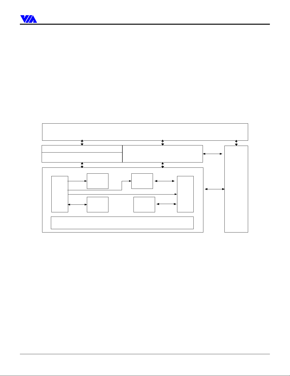
Register (Control/Status/Interrupt)
OVERVIEW
The VT6305 IEEE 1394 Open HCI Link Controller provides high performance serial connectivity. It implements the Link layer
for IEEE 1394.A release v1.0 and is compliant with Open HCI with DMA engine support for high performance data transfer. It
has a PCI host bus interface.
The VT6305 supports 100, 200 and 400 Mbits/sec transmission. Depending on transmission speed, the Link / PHY connection
is provided through a 2- / 4- / 8-bit interface operating at 50 MHz. The VT6305 services two types of data packets: asynchronous
and isochronous (real time). The 1394 link core performs arbitration requesting, packet generation and checking, and bus cycle
master operations. It also has root node capability and performs cycle and retry operations.
The VT6305 is ready to provide industry-standard IEEE 1394 peripheral connections for desktop and mobile PC platforms.
Support for the VT6305 will be built into Microsoft Windows 98 (Memphis) and Windows NT 5.0.
PCI 2.1 Host Interface
SWAP
Tx/Rx FIFO
Iso/Asy
DMA
Receiver
CRC
Checker
Cycle
Monitor
Link/PHY Interface
Cycle
Timer
CRC
Generator
Figure 1. VT6305 Chip Block Diagram
Transmitter
Revision 0.2 March 10, 2000 -2- Overview
Page 8
Technologies, Inc.
We ConnectWe Connect
FRAME#
DEVSEL#
REMREQ3#
PWREN_D3
LK_EN3
LK_EN2
STS_D3
E3PRSN3#
USBPRSN3#
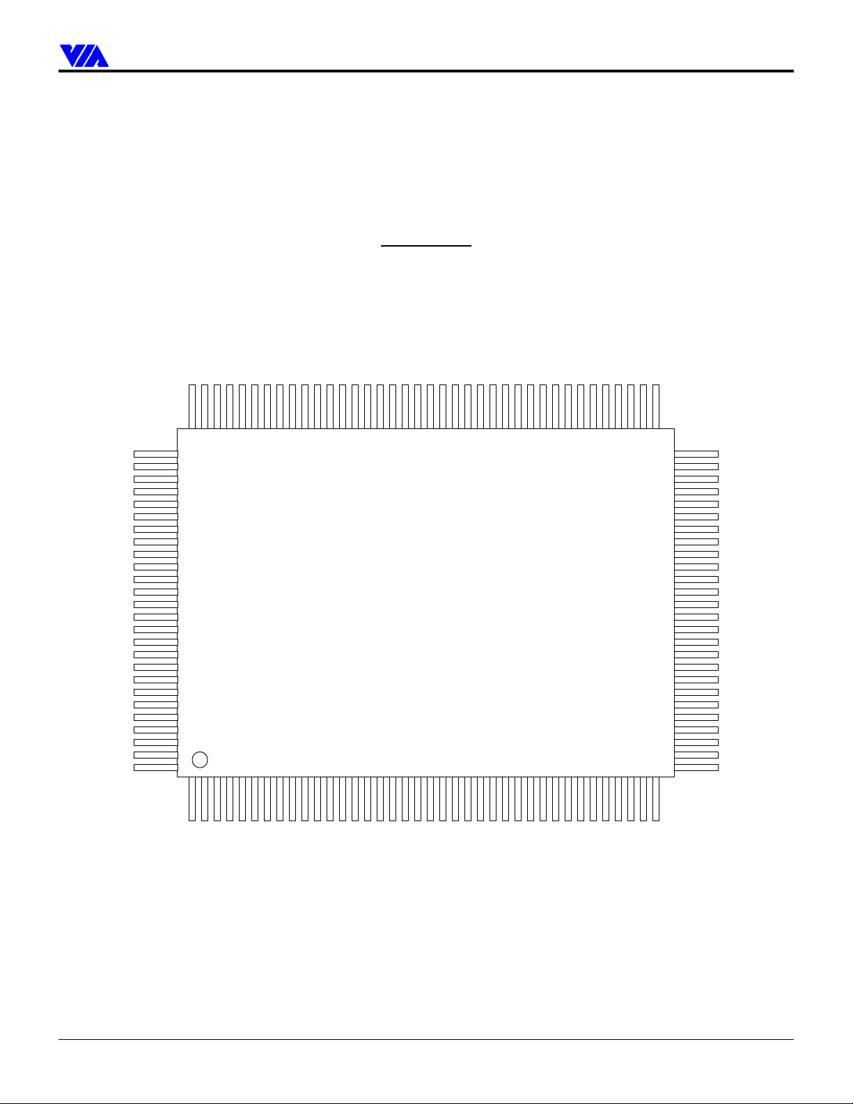
PINOUTS
Pin Diagram
STS_D2
E3PRSN2#
USBPRSN2#
REMREQ2#
PWREN_D2
REMREQ1#
PWREN_D1
LK_EN1
USBPRSN1#
E3PRSN1#
STS_D1
REMREQ0#
PWREN_D0
LK_EN0
USBPRSN0#
E3PRSN0#MD4/
VSS12
PHY_CLK
VDD9
PHY_D0
PHY_D1
PHY_D2
PHY_D3
VSS13
PHY_D4
PHY_D5
PHY_D6
PHY_D7
VSS14
PHY_CTL0
PHY_CTL1
VDD10
PHY_LREQ
LINK_ON
INTB#
INTA#
PCIRST#
PCICLK
VSS15
GNT#
REQ#
PME#
103
105
110
115
120
125
128
VSSC2
1
0
2
1
LPS
PCI_ISO
VDDC2
1
0
0
GPIO4
5
VSS11
GPIO2/
GPIO3/
9
5
MA14/
MA15/
1
0
VDD8
MA13/
9
0
VSS10
MA10/
MA12/
MA11/
VT6305
1
5
MA9/
MA8/
8
5
MA7/
MA6/
2
0
MA5/
MA4/
8
0
VSS9
MA3/
2
5
VDD7
MA2/
MA0/
MA1/
7
5
BPRD#
BPCS#
BPWR#
3
0
VSS8
GPIO1/
7
0
MD6/
MD7/
3
5
MD5/
6
5
3
8
VDD6
64
60
55
50
45
39
MD3/
MD2/
VSS7
MD1/
MD0/
EECS
AD0
AD1
AD2
AD3
VSS6
AD4
VDD5
AD5
AD6
AD7
CBE0#
AD8
AD9
VSS5
AD10
AD11
AD12
AD13
VDD4
AD14
STS_D0
EECK
EEDI
EEDO
AD31
AD30
AD29
VDD1
AD28
VSS1
AD27
AD26
AD25
AD24
IDSEL
CEB3#
AD23
VSS2
AD22
VDD2
AD21
AD20
AD19
AD18
AD17
AD16
VSS3
CBE2#
VDD3
IRDY#
TRDY#
STOP#
VSS4
PERR#
SERR#
PAR
CBE1#
AD15
VDDC1
VSSC1
Figure 2. VT6305 Pin Diagram (Top View)
Revision 0.2 March 10, 2000 -3- Pinouts
Page 9
Technologies, Inc.
We ConnectWe Connect
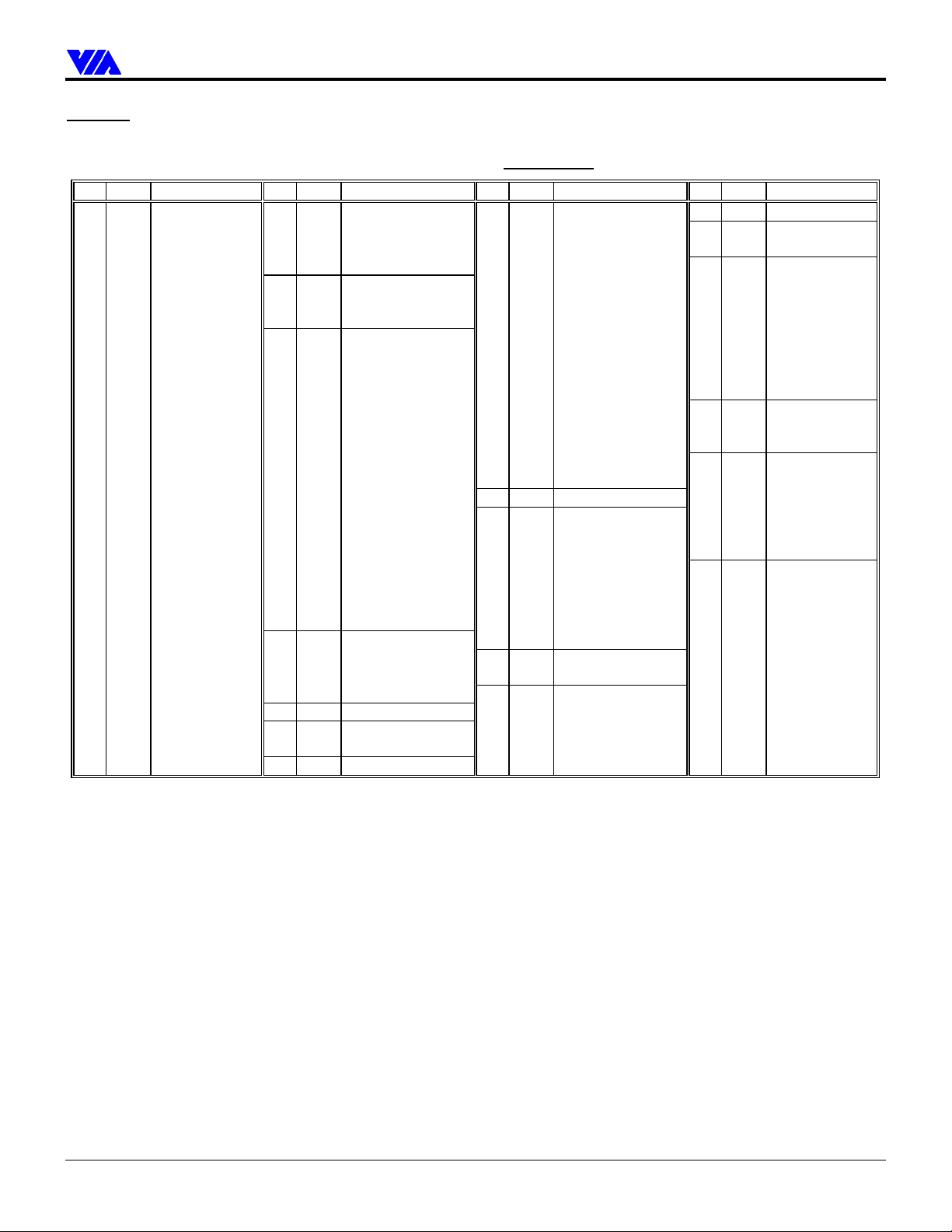
Pin List
Figure 3. VT6305 Pin List (Alphabetical Order)
Pin Pin Name Pin Pin Name Pin Pin Name Pin Pin Name
58 IO AD00 48 IO CBE0# 75 O / I MA00 / DB1SLK 104 I PHYCLK
57 IO AD01 35 IO CBE1# 76 O / I MA01 / DB11394# 116 IO PHYCTL0
56 IO AD02 24 IO CBE2# 77 O / I MA02 / DB1USB# 117 IO PHYCTL1
55 IO AD03 11 IO CBE3# 79 O / I MA03 / DB1RRQ# 106 IO PHYD0
53 IO AD04 29 IO DEVSEL# 81 O / O MA04 / DB1PEN 107 IO PHYD1
51 IO AD05 59 O EECS# 82 O / O MA05 / DB1LEN 108 IO PHYD2
50 IO AD06 25 IO FRAME# 83 O / I MA06 / DB2SLK 109 IO PHYD3
49 IO AD07
47 IO AD08
46 IO AD09
44 IO AD10
43 IO AD11
42 IO AD12
41 IO AD13
39 IO AD14
36 IO AD15
22 IO AD16
21 IO AD17
20 IO AD18
19 IO AD19
18 IO AD20
17 IO AD21
15 IO AD22
13 IO AD23
10 IO AD24 70 IO / O GPIO1 / DB0LEN 69 IO / O MD7 / DB0PEN
9 IO AD25 96 IO / O GPIO2 / DB3PEN 73 O MRD#
8 IO AD26 97 IO / O GPIO3 / DB3LEN 72 O MWR#
7 IO AD27 98 IO GPIO4 34 IO PAR
5 IO AD28 12 O IDSEL 99 IO PCIISO
4 IO AD29 122 O INTA# 124 I PCLK
2 IO AD30 121 O INTB# 31 O PERR#
1 IO AD31 27 IO IRDY# 126 I PGNT#
6 P GND
14 P GND
23 P GND
33 P GND
38 P GND
45 P GND
54 P GND
62 P GND
71 P GND
80 P GND
87 P GND
95 P GND
102 P GND
103 P GND
110 P GND
115 P GND
125 P GND
84 O / I MA07 / DB21394# 111 IO PHYD4
85 O / I MA08 / DB2USB# 112 IO PHYD5
86 O / I MA09 / DB2RRQ# 113 IO PHYD6
88 O / O MA10 / DB2PEN 114 IO PHYD7
89 O / O MA11 / DB2LEN 120 I PHYLON
90 O / I MA12 / DB3SLK 100 I PHYLPS
92 O / I MA13 / DB31394# 119 O PHYLREQ
93 O / I MA14 / DB3USB# 128 O PME#
94 O / I MA15 / DB3RRQ# 127 O PREQ#
74 O MCS# 123 I RESET#
60 IO / O MD0 / EEDO 32 O SERR#
61 IO / I MD1 / EEDI 30 IO STOP#
63 IO / O MD2 / EECK 28 IO TRDY#
64 IO / I MD3 / DB0SLK
66 IO / I MD4 / DB01394#
67 IO / I MD5 / DB0USB#
68 IO / I MD6 / DB0RRQ#
3 P VCC
16 P VCC
26 P VCC
37 P VCC
40 P VCC
52 P VCC
65 P VCC
78 P VCC
91 P VCC
101 P VCC
105 P VCC
118 P VCC
Revision 0.2 March 10, 2000 -4- Pinouts
Page 10
Technologies, Inc.
We ConnectWe Connect
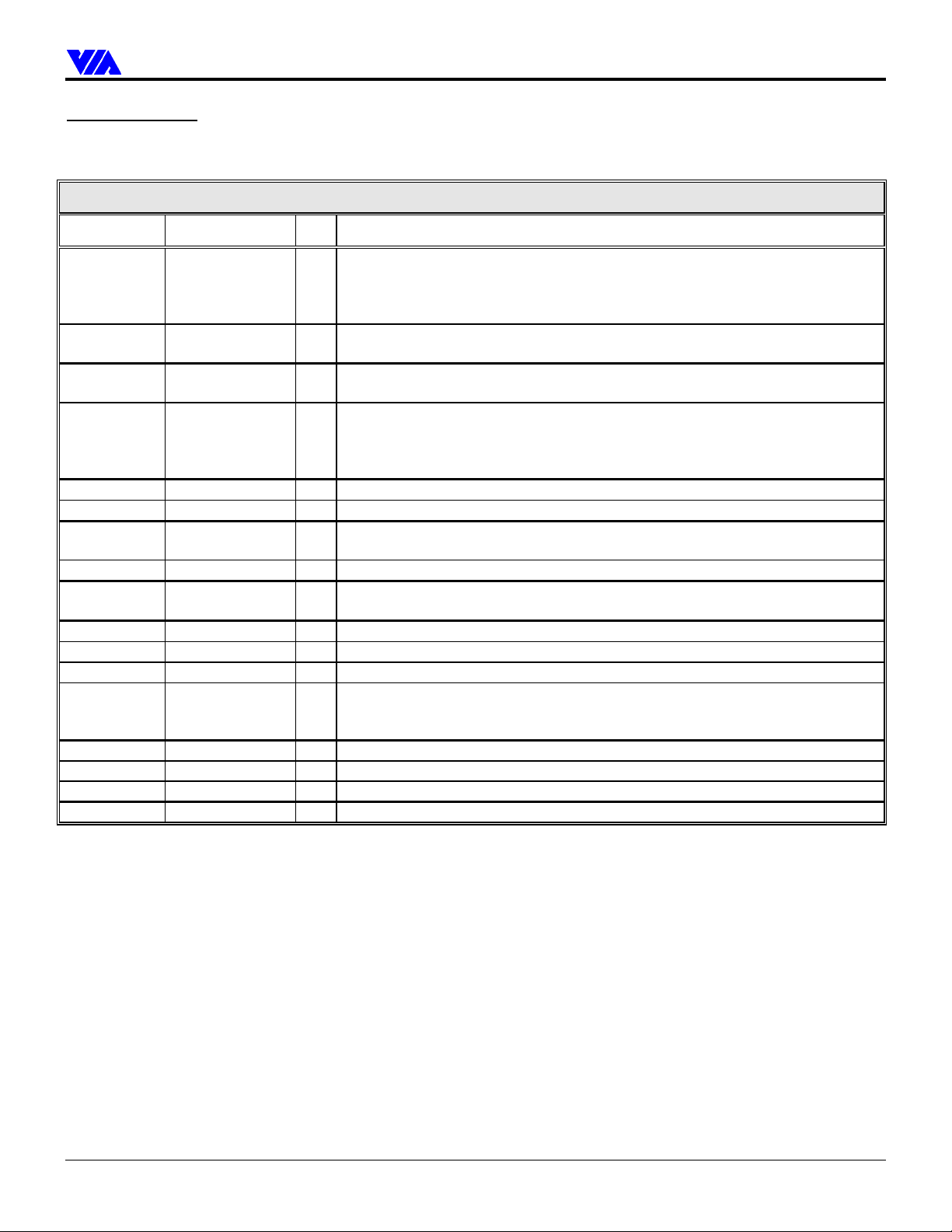
Pin Descriptions
Table 1. VT6305 Pin Descriptions
PCI Bus Interface
Signal Name Pin No. I/O Signal Description
AD[31:0]
CBE[3:0]#
FRAME#
DEVSEL#
TRDY#
IRDY#
PREQ#
PGNT#
IDSEL
INTA#
INTB#
PCLK
RESET#
PAR
PERR#
SERR#
STOP#
1, 2, 4, 5, 7-10,
13, 15, 17-22, 36,
39, 41-44, 46, 47,
49-51, 53, 55-58
11, 24, 35, 48 IO
25 IO
29 IO
28 IO
27 IO
127 O
126 I
12 O
122 O
121 O
124 I
123 I
34 IO
31 O
32 O
30 IO
IO
Address / Data Bus. The standard PCI address and data lines. The address is
driven with FRAME# assertion and data is driven or received in following cycles.
Command / Byte Enable. The command is driven with FRAME# assertion. Byte
enables corresponding to supplied or requested data are driven on following clocks.
Frame. Assertion indicates the address phase of a PCI transfer. Negation indicates
that one more data transfer is desired by the cycle initiator.
Device Select. As an output, this signal is asserted to claim PCI transactions
through positive or subtractive decoding. As an input, DEVSEL# indicates the
response to a VT6305-initiated transaction and is also sampled when decoding
whether to subtractively decode the cycle.
Target Ready. Asserted when the target is ready for data transfer.
Initiator Ready. Asserted when the initiator is ready for data transfer.
PCI Bus Request. Asserted by the bus master to indicate to the bus arbiter that it
wants to use the bus.
PCI Bus Grant. Asserted to indicate that access to the bus is granted.
Initialization Device Select. IDSEL is used as a chip select during configuration
read and write cycles.
Interrupt A. An asynchronous signal used to request an interrupt.
Interrupt B. An asynchronous signal used to request an interrupt.
PCI Clock. Timing reference for all transactions on the PCI Bus.
Reset. When detected low, an internal hardware reset is performed. PCIRST#
assertion or deassertion may be asynchronous to PCLK, however, it is recommended
that deassertion be synchronous to guarantee a clean and bounce free edge.
Parity. A single parity bit is provided over AD[31:0] and C/BE[3:0]#.
Parity Error. Parity error is asserted when a data parity error is detected.
System Error. SERR# is pulsed active to indicate a system error condition.
Stop. Asserted by the target to request the master to stop the current transaction.
Revision 0.2 March 10, 2000 -5- Pinouts
Page 11
Technologies, Inc.
We ConnectWe Connect
1394 PHY Interface
Signal Name Pin No. I/O Signal Description
PHYD[7:0]
PHYCTL1
PHYCTL0
PHYCLK
PHYLREQ
PHYLON
PHYLPS
114, 113, 112, 111,
109, 108, 107, 106
117 IO
116 IO
104 I
119 O
120 I
100 I
IO
PHY Data.
PHY Control 1.
PHY Control 0.
PHY Clock.
PHY Link Request.
PHY Link On.
PHY Link
Serial Configuration Memory Interface
Signal Name Pin No. I/O Signal Description
EECS#
EEDO / MD0
EEDI / MD1
EECK / MD2
59 O
60 O / I
61 I / I
63 O / I
EEPROM Chip Select. Chip select for external serial EEPROM when used to
provide configuration data. A high-value pull-up resistor is provided internally.
EEPROM Data Out.
EEPROM Data In.
EEPROM Clock.
Local Memory Interface
Signal Name Pin No. I/O Signal Description
MD[7:0]
MA[15:0]
MCS#
MRD#
MWR#
74 O
73 O
72 O
IO
O
Memory Data. Pins optionally used for device bay if local memory not used
Memory Address. Pins optionally used for device bay if local memory not used
Memory Chip Select.
Memory Read Enable.
Memory Write Enable.
Miscellaneous
Signal Name Pin No. I/O Signal Description
PME#
PCIISO
GPIO1 / DB0LEN
GPIO2 / DB3PEN
GPIO3 / DB3LEN
GPIO4
128 O
99 IO
70 IO / O
96 IO / O
97 IO / O
98 IO
Power Management Event.
General Purpose I/O.
General Purpose I/O.
General Purpose I/O.
General Purpose I/O.
General Purpose I/O.
Power and Ground
Signal Name Pin No. I/O Signal Description
Revision 0.2 March 10, 2000 -6- Pinouts
Page 12

Technologies, Inc.
We ConnectWe Connect
VCC
GND
3, 16, 26, 37, 40,
52, 65, 78, 91,
101, 105, 118
6, 14, 23, 33, 38,
45, 54, 62, 71, 80,
87, 95, 102, 103,
110, 115, 125
P
Power.
P
Ground.
Revision 0.2 March 10, 2000 -7- Pinouts
Page 13
Technologies, Inc.
We ConnectWe Connect
Offset
PCI Configuration Space Header
Default
Acc
Offset
Heading
Default
Acc
REGISTERS
Register Overview
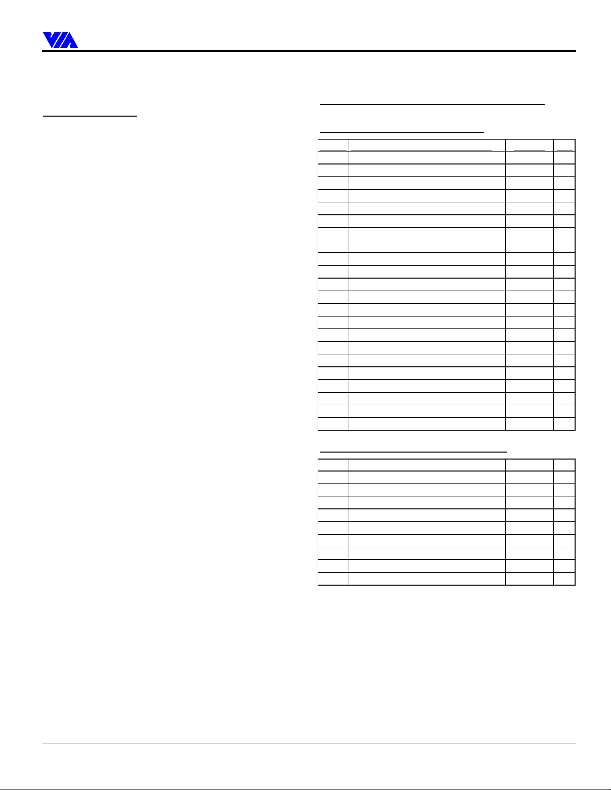
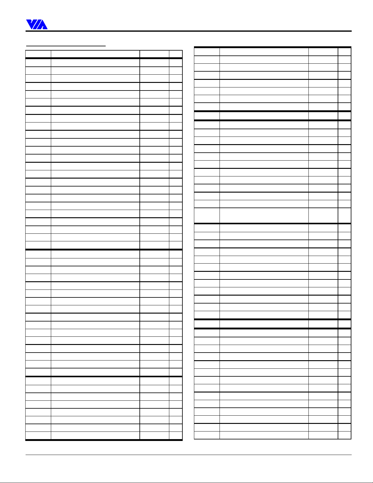
The following tables summarize the configuration and I/O
registers of the VT6305. These tables also document the
power-on default value (“Default”) and access type (“Acc”) for
each register. Access type definitions used are RW
(Read/Write), RO (Read/Only), “—” for reserved / used
(essentially the same as RO), and RWC (or just WC) (Read /
Write 1’s to Clear individual bits). Registers indicated as RW
may have some read/only bits that always read back a fixed
value (usually 0 if unused); registers designated as RWC or
WC may have some read-only or read write bits (see
individual register descriptions for details).
Detailed register descriptions are provided in the following
section of this document. All offset and default values are
shown in hexadecimal unless otherwise indicated
Table 2. Registers
PCI Function 0 Registers – Controller Configuration
Configuration Space Header Registers
1-0 Vendor ID 1106 RO
3-2 Device ID 0130 RO
5-4 Command 0000
7-6 Status 0280
8 Revision ID nn RO
9 Programming Interface 10 RO
A Sub Class Code 00 RO
B Base Class Code 0C RO
C -reserved- (cache line size) 00 —
D Latency Timer 00
E Header Type 00 RO
F -reserved- (Built In Self Test) 00 —
13-10 Base Address Register 0000 0000
14-27 -reserved- (base address registers) 00 —
28-2B -reserved- (unassigned) 00 —
2C-2F -reserved- (subsystem ID read) 00 —
30-33 -reserved- (expan. ROM base addr) 00 —
34-3B -reserved- (unassigned) 00 —
3C Interrupt Line 00
3D Interrupt Pin 01 RO
3E -reserved- (min gnt) 00 —
3F -reserved- (max lat) 00 —
RW
WC
RW
RW
RW
Controller-Specific Configuration Registers
43-40 PCI HCI Control 0000 0000
44 Miscellaneous Control 00 RW
45 -reserved- 00 —
46 PHY Control 00 RW
47-F3 -reserved- 00 —
F4 Hide Function Register 00 RW
F5-F7 -reserved- 00 —
FB-F8 Manufacturer ID TBD
FC-FF -reserved- 00 —
RO
RO
Revision 0.2 March 10, 2000 -8- Register Overview
Page 14
Technologies, Inc.
We ConnectWe Connect
Offset
Heading
Default
Acc
1394 Memory-Space Registers
0 Version 0000 0000
4 -reserved- (GUID ROM) 0000 0000 —
8 Asynchronous Transmit Retries 0000 0000 RW
C CSR Data 0000 0000 RW
10 CSR Compare Data 0000 0000 RW
14 CSR Control 8000 0000 RW
18 Configuration ROM Header 0000 0000 RW
1C 1394 Bus ID 3133 3934
20 1394 Bus Options F000 0002 RW
24 Global Unique ID High 0000 0000 RW
28 Global Unique ID Low 0000 0000 RW
2C-33 -reserved- 00 —
34 Configuration ROM Map 0000 0000 RW
38 Posted Write Address Low 0000 0000
3C Posted Write Address High 0000 0000
40 Vendor ID 0000 0000
44-4F -reserved- 00 —
50 HC Control Set 0000 0000 RW
54 HC Control Clear 0000 0000 RW
58-5F -reserved- 00 —
60-63 -reserved- 00 —
64 Self-ID Buffer Pointer 0000 0000 RW
68 Self-ID Count 0000 0000
6C-6F -reserved- 00 —
70 Isoch Rcv Channel Mask High Set 0000 0000 RW
74 Isoch Rcv Channel Mask High Clr 0000 0000 RW
78 Isoch Rcv Channel Mask Low Set 0000 0000 RW
7C Isoch Rcv Channel Mask Low Clr 0000 0000 RW
80 Interrupt Event Set 0000 0000 RW
84 Interrupt Event Clear 0000 0000 RW
88 Interrupt Mask Set 0000 0000 RW
8C Interrupt Mask Clear 0000 0000 RW
90 Isoch Xmit Interrupt Event Set 0000 0000 RW
94 Isoch Xmit Interrupt Event Clear 0000 0000 RW
98 Isoch Xmit Interrupt Mask Set 0000 0000 RW
9C Isoch Xmit Interrupt Mask Clear 0000 0000 RW
A0 Isoch Rcv Interrupt Event Set 0000 0000 RW
A4 Isoch Rcv Interrupt Event Clear 0000 0000 RW
A8 Isoch Rcv Interrupt Mask Set 0000 0000 RW
AC Isoch Rcv Interrupt Mask Clear 0000 0000 RW
B0-DB -reserved- 00 —
DC Fairness Control 0000 0000 RW
E0 Link Control Set 0000 0000 RW
E4 Link Control Clear 0000 0000 RW
E8 Node ID 0000 0000 RW
EC PHY Control 0000 0000 RW
F0 Isochronous Cycle Timer 0000 0000 RW
F4-FF -reserved- 00 —
RO
RO
RO
RO
RO
RO
100 Async Request Filter High Set 0000 0000 RW
104 Async Request Filter High Clear 0000 0000 RW
108 Async Request Filter Low Set 0000 0000 RW
10C Async Request Filter Low Clear 0000 0000 RW
110 Physical Request Filter High Set 0000 0000 RW
114 Physical Request Filter High Clear 0000 0000 RW
118 Physical Request Filter Low Set 0000 0000 RW
11C Physical Request Filter Low Clear 0000 0000 RW
120-17F -reserved- 00 —
180 Async Request Xmit Context Set 0000 0000 RW
184 Async Request Xmit Context Clr 0000 0000 RW
18C Async Request Xmit Command Ptr 0000 0000 RW
1A0 Async Response Xmit Context Set 0000 0000 RW
1A4 Async Response Xmit Context Clr 0000 0000 RW
1AC Async Response Xmit Cmd Ptr 0000 0000 RW
1C0 Async Request Rcv Context Set 0000 0000 RW
1C4 Async Request Rcv Context Clr 0000 0000 RW
1CC Async Request Rcv Command Ptr 0000 0000 RW
1E0 Async Response Rcv Context Set 0000 0000 RW
1E4 Async Response Rcv Context Clr 0000 0000 RW
1EC Async Response Rcv Command
0000 0000 RW
Ptr
200 Isoch Xmit Context 0 Set 0000 0000 RW
204 Isoch Xmit Context 0 Clr 0000 0000 RW
20C Isoch Xmit Context 0 Cmd Ptr 0000 0000 RW
210 Isoch Xmit Context 1 Set 0000 0000 RW
214 Isoch Xmit Context 1 Clr 0000 0000 RW
21C Isoch Xmit Context 1 Cmd Ptr 0000 0000 RW
220 Isoch Xmit Context 1 Set 0000 0000 RW
224 Isoch Xmit Context 1 Clr 0000 0000 RW
22C Isoch Xmit Context 1 Cmd Ptr 0000 0000 RW
230 Isoch Xmit Context 2 Set 0000 0000 RW
234 Isoch Xmit Context 2 Clr 0000 0000 RW
23C Isoch Xmit Context 2 Cmd Ptr 0000 0000 RW
250-3FF -reserved- 00 —
400 Isoch Rcv Context 0 Set 0000 0000 RW
404 Isoch Rcv Context 0 Clr 0000 0000 RW
40C Isoch Rcv Context 0 Command Ptr 0000 0000 RW
410 Isoch Rcv Context 0 Match 0000 0000 RW
420 Isoch Rcv Context 1 Set 0000 0000 RW
424 Isoch Rcv Context 1 Clr 0000 0000 RW
42C Isoch Rcv Context 1 Command Ptr 0000 0000 RW
430 Isoch Rcv Context 1 Match 0000 0000 RW
440 Isoch Rcv Context 2 Set 0000 0000 RW
444 Isoch Rcv Context 2 Clr 0000 0000 RW
44C Isoch Rcv Context 2 Command Ptr 0000 0000 RW
450 Isoch Rcv Context 2 Match 0000 0000 RW
460 Isoch Rcv Context 3 Set 0000 0000 RW
464 Isoch Rcv Context 3 Clr 0000 0000 RW
Revision 0.2 March 10, 2000 -9- Register Overview
Page 15

Technologies, Inc.
We ConnectWe Connect
46C Isoch Rcv Context 3 Command Ptr 0000 0000 RW
470 Isoch Rcv Context 3 Match 0000 0000 RW
480-7FF -reserved- 00 —
Revision 0.2 March 10, 2000 -10- Register Overview
Page 16

Technologies, Inc.
We ConnectWe Connect
Register Descriptions
1394 Host Controller Configuration Registers (Function 0)
The 1394 host controller interface follows the Open HCI
(OHCI) interface specification. There are two sets of software
accessible registers: configuration registers and memory
registers. The configuration registers are located in the
function 0 PCI configuration space. The memory registers
are located in system memory space at offsets from the
address stored in the Base Address Register.
Configuration Space Header
Offset 1-0 - Vendor ID .................................................... RO
0-7 Vendor ID ................(1106h = VIA Technologies)
Offset 3-2 - Device ID ...................................................... RO
0-7 Device ID (0130h = VT6305 1394 Controller)
Offset 5-4 - Command .................................................... RW
15-10 Reserved ...................................... always reads 0
9 Fast Back-to-Back Enable .......fixed at 0 (disabled)
8 SERR# Enable..........................fixed at 0 (disabled)
7 Wait Cycle Control...................fixed at 0 (disabled)
6 Parity Error Response..............fixed at 0 (disabled)
5 VGA Palette Snoop ...................fixed at 0 (disabled)
4 Postable Memory Write Enablefixed at 0 (disabled)
3 Special Cycle Enable................fixed at 0 (disabled)
2 Bus Master Enable
0 Disable.................................................default
1 Enable
1 Memory Space Enable
0 Disable.................................................default
1 Enable Access to 1394 Memory Registers
0 I/O Space Enable...................... fixed at 0 (disabled)
Offset 7-6 - Status ........................................................ RWC
15 Detected Parity Error.......................always reads 0
14 Signalled System Error..................... always reads 0
13 Received Master Abort
0 No Master Abort Generated.................. default
1 Master Abort Generated by 1394 Controller.
Set by the 1394 interface logic if it generates a
master abort while acting as a master. This
bit may be cleared by software by writing a
one to this bit position.
12 Received Target Abort
0 No Target Abort Received.................... default
1 Target Abort Received by 1394 Controller.
Set by the 1394 interface logic if it receives a
target abort while acting as a master. This bit
may be cleared by software by writing a one to
this bit position.
11 Signalled Target Abort.....................always reads 0
10-9 DEVSEL# Timing
00 Fast
01 Medium.................................................. fixed
10 Slow
11 Reserved
8 Data Parity Error Detected.............. always reads 0
7 Fast Back-to-Back Capable ..............always reads 1
6 User Definable Features ...................always reads 0
5 66 MHz Capable...............................always reads 0
4-0 Reserved ......................................always reads 0
Offset 8 - Revision ID (nnh) ............................................ RO
7-0 Silicon Revision Code (0 indicates first silicon)
Offset 9 - Programming Interface (10h=OHCI) ............. RO
Offset A - Sub Class Code (00h=1394 Serial Bus) .......... RO
Offset B - Base Class Code (0Ch=Serial Bus Controller) RO
Revision 0.2 March 10, 2000 -11- Register Descriptions
Page 17

Technologies, Inc.
We ConnectWe Connect
Offset D - Latency Timer (00h) ..................................... RW
7-4 Latency Timer Count
PCI burst cycles generated by the VT6305 can last
indefinitely as long as PCI GNT# remains active. If
GNT# is negated after the burst is initiated, the
VT6305 limits the duration of the burst to the
number of PCI Bus clocks specified in this field.
3-0 Reserved ......................................always reads 0
Offset E - Header Type (00h) ......................................... RO
Offset 13-10 - Base Address – 1394 Register Space ...... RW
31-7 Base Address (128-Byte Space).............. default = 0
6-4 Reserved ......................................always reads 0
3 Prefetechable.................................... always reads 0
Reads 0 to indicate that the 1394 register space is not
prefetchable.
2-1 Type ...................................... always reads 0
Reads 0 to indicate that the 1394 register space may
be located anywhere in the 32-bit address space.
0 Resource Type..................................always reads 0
Reads 0 to indicate a request for memory space.
Offset 3C - Interrupt Line (00h) ..................................... RO
Offset 3D - Interrupt Pin (01h=Drives INTA#) ............... RO
Revision 0.2 March 10, 2000 -12- Register Descriptions
Page 18

Technologies, Inc.
We ConnectWe Connect
Controller-Specific Configuration Registers
Offset 43-40 –PCI HCI Control ...................................... RO
insert bit definitions here
Offset 44 – Miscellaneous Control ................................. RW
7-1 Reserved ......................................always reads 0
0 Lock GUID Registers
0 Global Unique ID Registers are RW .....default
1 Global Unique ID Registers are Read Only
Once set, this bit cannot be cleared except by PCI
Reset. The GUID registers are located in memory in
the 1394 register space.
Offset 46 – PHY Control ................................................ RW
7-2 Reserved ......................................always reads 0
1 Isolated
0 Direct Environment
1 Isolated Environment
0 Multiple Speed Concatenation Disable
0 Packets of different speeds may be
concatenated as long as the concatenation is
not down to an S100 PHY.
1 Only same speed packets may be concatenated
(packets of different speeds may not be)
Note: A default value of 0000 for bits 3-0 indicates that the
1394 interface is connected to a 1394a-compliant
PHY.
Offset F4 – Hide Function Control ................................ RW
7-1 Reserved ......................................always reads 0
0 Hide Function
0 1394 Function Visible ..........................default
1 1394 Function Hidden
If this bit is set, the 1394 function will be
hidden. All subsequent reads or writes to this
configuration space will then cause a master
abort to be generated. This bit can only be
cleared by a PCI reset.
Offset FB-F8 – Manufacturer ID ................................... RO
31-0 Manufacturer ID............................always reads ???
Revision 0.2 March 10, 2000 -13- Register Descriptions
Page 19

Technologies, Inc.
We ConnectWe Connect
1394 Host Controller Memory-Space Registers
These registers occupy a 2048-byte space in system memory
(offsets 0-7FFh). This address space begins at the address
contained in the 1394 Configuration Space “Base Address
Register” (Function 0 Configuration Space Offset 10h).
All registers must be accessed as 32-bit words on 32-bit
boundaries. Writes to reserved addresses have undefined
results and reads from reserved addresses return
indeterminate data. Unless specified otherwise, all register
fields default to 0 and are unchanged after a 1394 bus reset.
Some registers are designated as Set and Clear registers.
These registers are in pairs, where a read of either address
will return the current contents of the register. Data written
to the Set register address is assumed to be a bit mask where
one bits determine which bits should be set. Data written to
the Clear register address is assumed to be a bit mask where
one bits determine which bits should be cleared.
Memory Offset 0 – Version ............................................. RO
7-0 Reserved ......................................always reads 0
Memory Offset 8 – Asynchronous Transmit Retries ..... RW
31-29 Second Limit......................................................RO
Count in Seconds (modulo 8). These bits and the
Cycle Limit bits below define a time limit for retry
attempts when the outbound dual-phase retry
protocol is in use.
28-16 Cycle Limit .......................................................RO
Count in Cycles (modulo 8000). These bits and the
Second Limit bits above define a time limit for retry
attempts when the outbound dual-phase retry
protocol is in use.
15-12 Reserved ......................................always reads 0
11-8 Max Physical Response Retries .............default = 0
Specifies how many times to attempt to retry the
transmit operation for the physical response packet
when a “busy” or “ack_type_error” acknowledge is
received from the target node. This value is used
only for responses to physical requests.
7-4 Max AT Response Retries .....................default = 0
Specifies to the Asynchronous Transmit Response
subsystem how many times to attempt to retry the
transmit operation for the response packet when a
“busy” or “ack_type_error” acknowledge is received
from the target node. This value is used only for
responses sent by software via the Asynchronous
Transmit Response DMA context.
3-0 Max AT Request Retries ........................default = 0
Specifies to the Asynchronous Transmit DMA
Request subsystem how many times to attempt to
retry the transmit operation for a packet when a
“busy” or “ack_type_error” acknowledge is received
from the target node. This value is used only for
responses sent by software via the Asynchronous
Transmit Request DMA context.
Revision 0.2 March 10, 2000 -14- Register Descriptions
Page 20

Technologies, Inc.
We ConnectWe Connect
Autonomous CSR Resources
The VT6305 implements the 1394 “Compare-and-Swap” bus
management registers, the Configuration ROM Header, and
the “Bus Info Block”. It also allows access to the first 1K
bytes of the configuration ROM.
Atomic compare-and-swap transactions, when accessed from
the 1394 bus, are autonomous without software intervention.
To access these bus management resource registers via the
PCI bus, the software first loads the CSR Data register with a
new data value to be loaded, then it loads the CSR Compare
register with the expected value. Finally, it writes the CSR
Control register with the selected value of the resource. This
initiates a compare-and-swap operation. When complete, the
CSR Control register “done” bit will be set and the CSR Data
register will contain the value of the selected resource prior to
the host-initiated compare-and-swap operation.
Bus Management CSR Registers
1394 requires certain 1394 bus management resource
registers to be accesssible only via 32-bit read and 32-bit lock
(compare-and-swap) transactions. These special bus
management resource registers are implemented on-chip:
CSR Hardware or
CSR Address Select Register Name Bus Reset
FFFF F000 021C 00 Bus Manager ID 0000 003F
FFFF F000 0220 01 Bandwidth Available 0000 1333
FFFF F000 0224 10 Channels Available Hi FFFF FFFF
FFFF F000 0228 18 Channels Available Lo FFFF FFFF
CSR Address FFFF F000 021C – Bus Manager ID....... RW
31-6 Reserved ...................................... always reads 0
5-0 Bus Manager ID.................................default = 3Fh
Memory Offset C – CSR Data ....................................... RW
31-0 CSR Data .............................. default = undefined
Data to be stored if comparison is successful.
Memory Offset 10 – CSR Compare Data ...................... RW
31-0 CSR Compare Data ..................default = undefined
Data to be compared with existing value of CSR
resource.
Memory Offset 14 – CSR Control .................................. RW
31 CSR Done ............................................default = 1
Set when a compare-swap operation is completed.
Reset whenever this register is written.
30-2 Reserved ......................................always reads 0
1-0 CSR Resource Select................. default = undefined
00 Bus Manager ID
01 Bandwidth Available
10 Channels Available Hi
11 Channels Available Lo
Memory Offset 18 – Configuration ROM Header ........ RW
31-24 Bus Info Block Length............................default = 0
Length of the Bus Information Block in doublewords
23-16 CRC Length............................................default = 0
Length of the block protected by the CRC (a value of
4 indicates that the CRC only protects the
configuration ROM header).
15-0 ROM CRC Value
Default value loaded from GUID ROM if present
(default is undefined if GUID ROM is not present).
Must be set prior to setting the “HC Control” register
“Link Enable” bit.
CSR Address FFFF F000 0220 – Bandwidth Available RW
31-13 Reserved ...................................... always reads 0
12-0 Bandwidth Available...................... default = 1333h
CSR Address FFFF F000 0224 – Channels Avail Hi ..... RW
7-0 Reserved ......................................always reads 0
CSR Address FFFF F000 0228 – Channels Avail Lo .... RW
7-0 Reserved ......................................always reads 0
Revision 0.2 March 10, 2000 -15- Register Descriptions
Page 21

Technologies, Inc.
We ConnectWe Connect
Memory Offset 1C – 1394 Bus ID ................................... RO
This register maps to the 1st 32-bit word of the bus info
block.
31-0 Bus ID......always reads 31333934h (ASCII “1394”)
Memory Offset 20 – 1394 Bus Options .......................... RW
This register maps to the 2nd quadword of the bus info block.
31 Isochronous Resource Manager Capable
0 Not capable
1 Capable................................................default
30 Cycle Master Capable
0 Not capable
1 Capable................................................default
29 Isochronous Capable
0 Not capable
1 Capable................................................default
28 Bus Manager Capable
0 Not capable
1 Capable................................................default
27 Power Management Capable
0 Not capable .........................................default
1 Capable
26-24 Reserved ...................................... always reads 0
23-16 Cycle Clock Acc
1394 Bus Management Field. This field must be
written with valid data prior to setting the “HC
Control” register “link enable” bit.
15-12 Received Block Write Request Packet Max
Length
1394 Bus Management Field. This field must be
written with valid data prior to setting the “HC
Control” register “link enable” bit. Received block
write request packets with a length greater than the
value contained in this field may generate an
“ack_type_error”.
11-8 Reserved ...................................... always reads 0
7-6 Configuration ROM Changed Since Last Bus
Reset
0 Configuration ROM not changed .........default
1 Configuration ROM changed
5-3 Reserved ......................................always reads 0
2-0 Max Link Speed .................................default = 010
Memory Offset 24 – Global Unique ID High ................. RW
This register maps to the 3rd 32-bit word of the bus info
block. Contents are cleared by hardware reset but are not
affected by software reset. Read/Write if Rx44[0] is cleared,
Read/Only if Rx44[0] is set.
31-8 Node Vendor ID......................................default = 0
1394 Bus Management Field. Must be set prior to
setting the “HC Control” register “link enable” bit.
7-0 Chip ID High ..........................................default = 0
1394 Bus Management Field. Must be set prior to
setting the “HC Control” register “link enable” bit.
Memory Offset 28 – Global Unique ID Low .................. RW
This register maps to the 4th 32-bit word of the bus info
block. Contents are cleared by hardware reset but are not
affected by software reset. Read/Write if Rx44[0] is cleared,
Read/Only if Rx44[0] is set.
31-0 Chip ID Low ...........................................default = 0
1394 Bus Management Field. Must be set prior to
setting the “HC Control” register “link enable” bit.
Revision 0.2 March 10, 2000 -16- Register Descriptions
Page 22

Technologies, Inc.
We ConnectWe Connect
Memory Offset 34 – Configuration ROM Map............. RW
This register contains the start address within the memory
space that maps to the start address of the 1394 configuration
ROM. Only 32-bit word reads to the first 1K bytes of the
configuration ROM will map to memory space.(all other
transactions to this space will be rejected with an
“ack_type_error”). The system address of the configuration
ROM must start on a 1K-byte boundary. The first five 32-bit
words of the configuration ROM space are mapped to the
configuration ROM header and Bus Info Block, so the first
five registers addressed by this register are not used. This
register must be set to a valid address prior to setting the “HC
Control” register “link enable” bit.
31-10 Configuration ROM Address.................default = 0
Read requests to 1394 offsets FFFF F000 0400
through FFFF F000 03FC have the low-order 10 bits
of the offset added to this register to determine the
host memory address of the returned data value.
9-0 Reserved ......................................always reads 0
Memory Offset 38 – Posted Write Address Low ............ RO
31-0 Offset Low ...............................default = undefined
If the “Posted Write Error” bit is set in the Interrupt
Events register, this and the “Posted Write Address
High” register contain the 48 bits of the 1394
destination offset of the write request that resulted in
the PCI error.
Memory Offset 3C – Posted Write Address High .......... RO
31-16 Source ID ...............................default = undefined
The Bus Number and Node Number of the node
which has issued the failed write request.
15-0 Offset High ...............................default = undefined
If the “Posted Write Error” bit is set in the Interrupt
Events register, this and the “Posted Write Address
Low” register contain the 48 bits of the 1394
destination offset of the write request that resulted in
the PCI error.
Memory Offset 40 – Vendor ID ...................................... RO
31-0 Vendor ID .................................always reads TBD
HC Control Registers
The following two registers are a “set / clear” register pair.
Writing to the “Set” register address sets selected bits in the
control register where the written bit value is 1. Writing to
the “Clear” register address clears selected bits in the control
register where the written bit value is 1. Reading from either
address returns the contents of the control register.
Memory Offset 50 (Set), 54 (Clear) – HC Control ........ RW
31-20 Reserved ......................................always reads 0
19 Link Power Status
0 Prohibit Link to PHY Communications .....def
1 Permit Link to PHY Communications (link
can use LREQs to perform PHY reads and
writes).
This bit has no effect on “Link On” status for the
node (see Link Enable status below). Both software
and hardware resets clear this bit.
18 Posted Write Enable.................default = undefined
0 All writes return “ack_pending”
1 Enable 2-deep posted write queue
Software should only change this bit when “Link
Enable” is 0.
17 Link Enable
0 Disable packets from being transmitted,
received, or processed........................... default
1 Enable packets to be transmitted, received,
and processed
Both software and hardware resets clear this bit.
Software should not set this bit until the
Configuration ROM mapping register is valid.
16 Soft Reset
When set, all on-chip 1394 states are reset, all FIFOs
are flushed, and all registers are set to their hardware
reset (default) values unless otherwise specified. PCI
configuration registers are not affected. Hardware
clears this bit automatically when the reset is
complete (it reads 1 while the reset is in progress).
15-0 Reserved ......................................always reads 0
Revision 0.2 March 10, 2000 -17- Register Descriptions
Page 23

Technologies, Inc.
We ConnectWe Connect
Self-ID Control Registers
Memory Offset 64 – Self ID Buffer Pointer .................. RW
31-11 Self-ID Buffer Pointer...............default = undefined
Contains the base address of a 2K-byte buffer in host
memory where received Self-ID packets are stored.
10-0 Reserved ...................................... always reads 0
Memory Offset 68 – Self ID Count ................................. RO
31 Self-ID Error.............................default = undefined
0 Self-ID packet received with no errors (this bit
is automatically cleared after error-free
reception of a Self-ID packet)
1 Error detected during most recent Self-ID
packet reception (the contents of the Self-ID
Buffer are undefined in this case)
30-24 Reserved ...................................... always reads 0
23-16 Self-ID Generation ....................default = undefined
The value in this field is incremented automatically
each time the Self-ID reception process begins. The
value rolls over after reaching 255.
15-13 Reserved ...................................... always reads 0
12-2 Self-ID Size ...............................default = undefined
Contains the length in 32-bit words of Self-ID data
that has been received. This field is cleared by 1394
bus reset.
1-0 Reserved ......................................always reads 0
Channel Mask Registers
Offset 70 (Set), 74 (Clear) – Iso Rcv Channel Mask Hi RW
31-0 Iso Channel Mask N+32 ...................default = 0000
Bits 31-0 correspond to channel numbers 63-32.
Writing 1 bits to offset 70 enables corresponding
channels for receiving isochronous data. Writing 1
bits to offset 74 disables corresponding channels
from receiving isochronous data.
Offset 78 (Set), 7C (Clear) – Iso Rcv Channel Mask Lo RW
31-0 Iso Channel Mask N+32 ...................default = 0000
Bits 31-0 correspond to channel numbers 31-0.
Writing 1 bits to offset 78 enables corresponding
channels for receiving isochronous data. Writing 1
bits to offset 7C disables corresponding channels
from receiving isochronous data.
Revision 0.2 March 10, 2000 -18- Register Descriptions
Page 24

Technologies, Inc.
We ConnectWe Connect
Interrupt Registers
Memory Offset 80 (Set), 84 (Clear) – Interrupt Events RW
31-27 Reserved ...................................... always reads 0
26 PHY Register Data Recieved
PHY register data byte received (data byte not sent
when register 0 received)
25 Cycle Too Long
More than 115 usec (but not more than 120 usec)
elapsed between the start of sending a cycle start
packet and the end of a subaction gap.
24 Unrecoverable Error
Error encountered that has forced the chip to stop
operations of any or all subunits (e.g., when a DMA
context sets its “ContextControl.Dead” bit)
23 Cycle Inconsistent
Cycle start received with a cycle count different from
the value in the “Cycle Timer” register
22 Cycle Lost
Expected cycle start not received (cycle start not
received immediately after the first subaction gap
after the “Cycle Sync” event or arbitration reset gap
detected after a “Cycle Sync” event without an
intervening cycle start).
21 Cycle 64 Seconds Interrupt
Bit 7 of the “Cycle Seconds Counter” has changed.
20 Cycle Synch Interrupt
New isochronous cycle started (least significant bit
of the cycle count toggled).
19 PHY Requested Interrupt
The PHY has requested an interrupt using a status
transfer.
18 Reserved ......................................always reads 0
17 Bus Reset Entered
The Phy has entered bus reset mode.
16 Self-ID Complete
Self-ID packet stream received.
15-10 Reserved ...................................... always reads 0
9 Lock Response Error
Lock response sent to a serial bus register in
response to a lock request but no “ack_complete”
received.
8 Posted Write Error
A host bus error occurred while the chip was trying
to write a 1394 write request (which had already
been given an “ack_complete”) into system memory.
7 Isochronous ReceiveDMA Complete
One or more Isochronous receive contexts have
generated an interrupt (one or more bits have been
set in the “Isochronous Receive Interrupt Event”
register masked by the “Isochronous Receive
Interrupt Mask” register).
6 Isochronous Transmit DMA Complete
One or more Isochronous transmit contexts have
generated an interrupt (one or more bits have been
set in the “Isochronous Transmit Interrupt Event”
register masked by the “Isochronous Transmit
Interrupt Mask” register).
5 Response Packet Sent
A packet was sent to an asynchronous receive
response context buffer.
4 Receive Packet Sent
A packet was sent to an asynchronous receive
request context buffer.
3 Async Receive Response DMA Complete
Conditionally set upon completion of an ARDMA
Response context command descriptor.
2 Async Receive Request DMA Complete
Conditionally set upon completion of an ARDMA
Request context command descriptor.
1 Async Response Transmit DMA Complete
Conditionally set upon completion of an ATDMA
Response command.
0 Async Request Transmit DMA Complete
Conditionally set upon completion of an ATDMA
Request command.
Memory Offset 88 (Set), 8C (Clear) – Interrupt Mask . RW
The bits in this register (except for the Master Interrupt
Enable bit in bit-31) correspond to the bits in the Interrupt
Event register above. Zeros in these bits prevent the
corresponding interrupt condition from generating an
interrupt. Bits are set in the mask register by writing one bits
to the “Set” address and cleared by writing one bits to the
“Clear” address. The current value of the mask bits may be
read from either address.
31 Master Interrupt Enable
0 Disable All Interrupt Events.................default
1 Generate interrupts per mask bits 0-26
30-27 Reserved ......................................always reads 0
26-0 Interrupt Mask .........................default = undefined
(see Interrupt Event register)
Revision 0.2 March 10, 2000 -19- Register Descriptions
Page 25

Technologies, Inc.
We ConnectWe Connect
Offset 90 (Set), 94 (Clear) – Iso Xmit Interrupt Events RW
31-4 Reserved ...................................... always reads 0
3-0 Isochronous Transmit Context .default = undefined
An interrupt is generated by an isochronous transmit
context if an “Output Last DMA” command
completes and its “i” bits are set to “interrupt
always”. Software clears the bits in this register by
writing one bits to the “Clear” address. Bits in this
register will only get set to one if the corresponding
bits in the mask register are set to one.
Offset 98 (Set), 9C (Clear) – Iso Xmit Interrupt Mask . RW
31-4 Reserved ...................................... always reads 0
3-0 Iso Transmit Context Mask.......default = undefined
Setting bits in this register enables interrupts to be
generated by the corresponding isochronous transmit
context
Offset A0 (Set), A4 (Clear) – Iso Rcv Interrupt Events. RW
31-4 Reserved ......................................always reads 0
3-0 Isochronous Receive Context ...default = undefined
An interrupt is generated by an isochronous receive
context if an “Input Last DMA” command completes
and its “i” bits are set to “interrupt always”.
Software clears the bits in this register by writing
one bits to the “Clear” address. Bits in this register
will only get set to one if the corresponding bits in
the mask register are set to one.
Offset A8 (Set), AC (Clear) – Iso Rcv Interrupt Mask . RW
31-4 Reserved ......................................always reads 0
3-0 Iso Receive Context Mask.........default = undefined
Setting bits in this register enables interrupts to be
generated by the corresponding isochronous receive
context
Revision 0.2 March 10, 2000 -20- Register Descriptions
Page 26

Technologies, Inc.
We ConnectWe Connect
Link Control Registers
Memory Offset DC – Fairness Control .......................... RO
31-8 Reserved ...................................... always reads 0
7-0 Requests Per Fairness Interval ..............default = 0
The number of request packets allowed to be
transmitted per fairness interval
Memory Offset E0 (Set), E4 (Clear) – Link Control .... RW
This register contains the control flags that enable and
configure the link core protocol portions of the chip. It
contains controls for the receiver and cycle timer.
31-22 Reserved ...................................... always reads 0
21 Cycle Master .............................default = undefined
0 Received cycle start packets will be accepted
to maintain synchronization with the node
that is sending them.
1 If the PHY has sent notification that it is root,
a cycle start packet will be generated every
time the cycle timer rolls over, based on the
setting of the “Cycle Source” bit.
This bit is cleared automatically if the “Cycle Too
Long” interrupt event occurs and cannot be set until
the “Cycle Too Long” interrupt event bit is cleared.
20 Cycle Timer Enable...................default = undefined
0 Cycle timer offset will not count
1 Cycle Timer offset will count cycles of the
24.576 MHz clock and roll over at the
appropriate time based on the settings of the
above bits
19-11 Reserved ...................................... always reads 0
10 Receive PHY Packet...............................default = 0
0 All PHY packets received outside of the self-
ID phase are ignored
1 The receiver will accept incoming PHY
packets into the AR request context if the AR
request context is enabled. This bit does not
control receipt of self-ID packets.
9 Receive Self-ID.......................................default = 0
0 All self-ID packets are ignored
1 The receiver will accept incoming self-
identification packets. Before setting this bit,
software must ensure that the self-ID buffer
pointer register contains a valid address.
8-0 Reserved ......................................always reads 0
Memory Offset E8 – Node ID......................................... RW
This register contains the CSR address for the node on which
this chip resides. The 16-bit combination of the Bus Number
and Node Number fields is referred to as the “Node ID”. The
Node Number field is updated when register 0 is sent from
the PHY. This can happen either because software requested
a read from the PHY through the PHY Control register or
because the PHY is sending the register (most likely due to a
bus reset).
31 ID Valid
0 No valid node number (cleared by bus reset)
1 Valid node number received from PHY
30 Root
This bit is set to 0 or 1 during bus reset
0 Attached PHY is not root........................... def
1 Attached PHY is root
29-28 Reserved ......................................always reads 0
27 Cable Power Status
0 PHY reports cable power status is not OK . def
1 PHY reports cable power status is OK.
26-16 Reserved ......................................always reads 0
15-6 Bus Number ............................................................
Used to identify the specific 1394 bus to which this
node belongs when multiple 1394-compatible buses
are connected via a bridge (set to 3FFh by bus reset)
5-0 Node Number..........................................default = 0
The physical node number established by the PHY
during self-identification and automatically set to the
value received from the PHY after the selfidentification phase. If the PHY sets this field to 63
(all ones), all link-level transmits are disabled.
Revision 0.2 March 10, 2000 -21- Register Descriptions
Page 27

Technologies, Inc.
We ConnectWe Connect
PHY Control Registers
Memory Offset EC – PHY Control ............................... RW
This register is used to read or write a PHY register. To read
or write, the address of the register is written into the Register
Address field. For reads the “Read Register” bit is set (when
the request has been sent to the PHY, the “Read Register” bit
is cleared automatically by the chip). When transmitting the
request, the first clock for LREQ for the register read/write
portion will be bit-11 of this register followed by bit-10, etc,
finishing with bit-8 for register reads and bit-0 for register
writes. When the PHY returns the register through a status
transfer, the “Read Done” bit is set. The address of the
register received is placed in the “Read Address” field and the
contents in the “Read Data” field. The first bits of data
received on the status transfer for the register are placed in
bits 27 (D[0]) and 26 (D[1]) of this register. For writes, the
value to write is written to the “Write Data” field and the
“Write Register” bit is set. The “Write Register” bit is
cleared automatically by the chip when the write request has
been sent to the PHY.
31 Read Done
Indicates that a read request has been completed and
valid information is contained in the Read Data and
Read Address fields. Cleared when the “Read
Register” bit is set. It is set by the chip when a
register transfer is received from the PHY.
30-28 Reserved ...................................... always reads 0
27-24 Read Address
The address of the register most recently received
from the PHY.
23-16 Read Data
The contents of the register most recently received
from the PHY
15 Read Register
Used to initiate a read request from a PHY register
(must not be set at the same time as the “Write
Register” bit). Cleared by the chip when the request
has been sent.
14 Write Register
Used to initiate a write request to a PHY register
(must not be set at the same time as the “Read
Register” bit). Cleared by the chip when the request
has been sent.
13-12 Reserved ...................................... always reads 0
11-8 Register Address
The address of the PHY register to be read or written
7-0 Write Data
The data to be written to the PHY (ignored for reads)
Cycle Timer Registers
Memory Offset F0 – Isochronous Cycle Timer.............. RW
This register shows the current cycle number and offset.
When the chip is cycle master, this register is transmitted
with the cycle start message. When it is not cycle master, this
register is loaded with the data field in an incoming cycle
start. In the event that the cycle start message is not received,
the fields continue incrementing on their own (when the
“Cycle Timer Enable” field is set in the “Link Control”
register) to maintain a local time reference.
31-25 Cycle Seconds .........................................default = 0
This field counts seconds (“Cycle Count” rollovers)
modulo 128.
24-12 Cycle Count ............................................default = 0
This field counts cycles (“Cycle Offset” rollovers)
modulo 8000.
11-0 Cycle Offset ............................................default = 0
This field counts 24.576 MHz clocks modulo 3072
(125 usec).
Revision 0.2 March 10, 2000 -22- Register Descriptions
Page 28

Technologies, Inc.
We ConnectWe Connect
Filter Registers
Offset 100 (Set), 104 (Clear) – Async Req Filter High.. RW
31 Async Request Resources All Buses
0 Asynchronous requests received from non-
local bus nodes will be accepted only if the bit
which is set corresponds to the node number
(see the remaining bits of this register and the
“Async Request Filter Low” register)...default
1 All asynchronous requests received from non-
local bus nodes will be accepted.
Bus reset does not affect the value of this bit
30-0 Async Request Resource “N”.................default = 0
If set to one for local bus node number N+32,
asynchronous requests received from that node
number will be accepted. The bit number
corresponds to the node number + 32. Bus reset sets
all bits of this field to 0.
Offset 108 (Set), 10C (Clear) – Async Req Filter Low .. RW
31-0 Async Request Resource “N”.................default = 0
If set to one for local bus node number N,
asynchronous requests received from that node
number will be accepted. The bit number
corresponds to the node number. Bus reset sets all
bits of this field to 0.
Offset 110 (Set), 114 (Clear) – Physical Req Filter High RW
31 Physical Request Resources All Buses
0 Asynchronous physical requests received from
non-local bus nodes will be accepted only if
the bit which is set corresponds to the node
number (see the remaining bits of this register
and the “Physical Request Filter Low”
register)................................................default
1 All asynchronous physical requests received
from non-local bus nodes will be accepted.
Bus reset does not affect the value of this bit.
30-0 Physical Request Resource “N”..............default = 0
If set to one for local bus node number N+32,
asynchronous physical requests received from that
node number will be accepted. The bit number
corresponds to the node number + 32. Bus reset sets
all bits of this field to 0.
Offset 118 (Set), 11C (Clear) – Physical Req Filter Low RW
31-0 Physical Request Resource “N”..............default = 0
If set to one for local bus node number N,
asynchronous physical requests received from that
node number will be accepted. The bit number
corresponds to the node number. Bus reset sets all
bits of this field to 0
Revision 0.2 March 10, 2000 -23- Register Descriptions
Page 29

Technologies, Inc.
We ConnectWe Connect
Asynchronous Transmit & Receive Context Registers
Offset 180 (Set), 184 (Clr) – Async Req Xmit Context.. RW
Offset 1A0 (Set), 1A4 (Clr) – Async Rsp Xmit Context RW
Offset 1C0 (Set), 1C4 (Clr) – Async Req Rcv Context .. RW
Offset 1E0 (Set), 1E4 (Clr) – Async Rsp Rcv Context .. RW
These registers are the Context Control registers for
Asynchronous Transmit Requests and Responses and
Asynchronous Receive Requests and Responses, respectively.
They contain bits for control of options, operational state, and
status for a DMA context. The bit layout for both registers is
given below:
31-16 Reserved ...................................... always reads 0
15 Run
This bit is set and cleared by software to enable
descriptor processing for a context. The chip will
clear this bit automatically on a hardware or software
reset. Before software sets this bit, the active bit
must be clear and the Command Pointer register for
the context must contain a valid descriptor block
address and a Z value that is appropriate for the
descriptor block address.
Software may stop the chip from further processing
of a context by clearing this bit. When cleared, the
chip will stop processing of the context in a manner
that will not impact the operation of any other
context or DMA controller. This may require a
significant amount of time. If software clears a run
bit for an isochronous context while the chip is
processing a packet for the context, it will continue
to receive or transmit the packet and update the
descriptor status. It will then stop at the conclusion
of that packet. If the run bit is cleared for a nonisochronous context, the chip will stop processing at
a convenient point and put the descriptors in a
consistent state (e.g., status updated if a packet was
sent and acknowledged).
Clearing the bit may have other side effects that are
DMA controller dependent. This is described in the
sections that cover each of the DMA controllers.
14-13 Reserved ...................................... always reads 0
12 Wake ............................................default = 0
When software adds to a list of descriptors for a
context, the chip may have already read the
descriptor that was at the end of the list before it was
updated. This bit provides a semaphore to indicate
that the list may have changed.
If the chip had fetched a descriptor and the indicated
branch address had a Z value of zero, it will reread
the pointer value when the wake bit is set. If, on the
reread, the Z value is still zero, then the end of the
list has been reached and the chip will clear the
active bit. If, however, the Z value is now non-zero,
the chip will continue processing. If the wake bit is
set while the chip is active and has a Z value of nonzero, it takes no special action.
The chip will clear this bit before it reads or rereads
a descriptor. The wake bit should not be set while
the run bit is zero.
11 Dead ............................................default = 0
This bit is set by the chip to indicate a fatal error in
processing a descriptor. When set, the active bit is
cleared. This bit is cleared when software clears the
run bit or on a hardware or software reset.
10 Active ............................................default = 0
This bit is set by the chip when software sets the run
bit or sets the wake bit while the run bit is set. The
chip will clear this bit:
1) when a branch is indicated by a descriptor but
the Z value of the branch address is 0
2) when software clears the run bit and the chip
has reached a safe stopping point
3) while the dead bit is set
4) after a hardware or software reset
5) for asynchronous transmit contexts (request
and response), when a bus reset occurs
When this bit is 0 and the run bit is 0, the chip will
set the Interrupt Event bit for the context.
9-8 Reserved ......................................always reads 0
7-5 Speed (Async Receive Contexts Only)
This field indicates the speed at which the packet
was received or transmitted:
000 100 Mbits/sec
001 200 Mbits/sec
010 400 Mbits/sec
011 -reserved1xx -reserved-
4-0 Ack / Err Code........................................default = 0
Following an “Output Last” command, the received
“Ack Code” or “Event Error Code” is indicated in
this field. Possible values are: “Ack Complete”,
“Ack Pending”, Ack Busy X”, “Ack Data Error”,
“Ack Type Error”, “Event Tcode Error”, “Event
Missing Ack”, “Event Underrun”, “Event Descriptor
Read”, “Event Data Read”, “Event Timeout”, “Event
Flushed”, and “Event Unknown” (see “Table 3.
Packet Event Codes” on the following page for
descriptions and values for these codes).
Offset 18C – Async Req Xmit Context Command Ptr .. RW
Offset 1AC – Async Rsp Xmit Context Command Ptr .. RW
Offset 1CC – Async Req Rcv Context Command Ptr.... RW
Offset 1EC – Async Rsp Rcv Context Command Ptr .... RW
Revision 0.2 March 10, 2000 -24- Register Descriptions
Page 30

Technologies, Inc.
We ConnectWe Connect
Table 3. Packet Event Codes
Code Name DMA Meaning
00/10
01/11
02/12
03/13
04/14
05/15
06/16
07/17
08/18
09/19
0A/1A
0B
0C-
0D/1B
-1D
0E/1E
0F/1F
11
12
13
14
15
16
17-1C
1D
1E
1F
Event Tcode Error
Event Short
Packet
Event Long Packet
Event Missing Ack
Event Underrun
Event Overrun
Event Descriptor
Read
Event Data Read
Event Data Write
Event Bus Reset
Event Timeout
Event Tcode Error
Reserved
Event Unknown
Event Flushed
Ack Complete
Ack Pending
Reserved
Ack Busy X
Ack Busy A
Ack Busy B
Reserved
Ack Data Error
Ack Type Error
Reserved
AT, AR,
A bad Tcode is associated with this packet. The packet was flushed.
IT, IR, IT
The received data length was less than the packet’s data length (IR packet-per-buffer
mode only).
IR The received data length was greater than the packet’s data length (IR packet-per-
buffer mode only).
AT A subaction gap was detected before an ack arrived
AT, IT An underrun occurred on the corresponding FIFO and the packet was truncated.
IR A receive FIFO overflowed during the reception of an isochronous packet.
AT, AR,
IT, IR
An unrecoverable error occurred while the Host Controller was reading a descriptor
block.
AT, IT An error occurred while the Host Controller was attempting to read from host memory
in the data stage of descriptor processing.
AR, IR, IT An error occurred while the Host Controller was attempting to write to host memory
in the data stage of descriptor processing.
AR Identifies a PHY packet in the receive buffer as being the synthesized bus reset packet
AT Indicates that the asynchronous transmit response packet expired and was not
transmitted
AT A bad Tcode is associated with this packet. The packet was flushed.
AT, AR,
IT, IR
An error condition has occurred that cannot be represented by any other defined event
codes
AT Sent by the link side of the output FIFO when asynchronous packets are being flushed
due to a bus reset
AT, AR,
IT, IR
The destination node has successfully accepted the packet. If the packet was a request
subaction, the destination node has successfully completed the transaction and no
response subaction shall follow.
The ack / err code for transmitted PHY, isochronous and broadcast packets, none of
which yield an ack code, will be set by hardware to “Ack Complete” unless an “Event
Underrun” or “Event Data Read” occurs.
AT, AR The destination node has successfully accepted the packet. If the packet was a request
subaction, a response subaction will follow at a later time. This code is not returned
for a response subaction.
AT The packet could not be accepted after max “ATretries” attempts and the last ack
received was “Ack Busy X.”
AT The packet could not be accepted after max “ATretries” attempts and the last ack
received was “Ack Busy A." OHCI does not support the dual phase retry protocol for
transmitted packets, so this ack should not be received.
AT The packet could not be accepted after max “ATretries” attempts and the last ack
received was “Ack Busy B" (see note for “Ack Busy A”).
AT, IR The destination node could not accept the block packet because the data field failed
the CRC check or because the length of the data block payload did not match the
length contained in the “Data Length” field. This code is not returned for any packet
that does not have a data blocik payload.
AT, AR Returned when a received block write request or received block read request is greater
than “max_rec”
Revision 0.2 March 10, 2000 -25- Register Descriptions
Page 31

Technologies, Inc.
We ConnectWe Connect
Isochronous Transmit Context Registers
Offset 200 (Set), 204 (Clr) – Isoch Xmit Context 0........ RW
Offset 210 (Set), 214 (Clr) – Isoch Xmit Context 1........ RW
Offset 220 (Set), 224 (Clr) – Isoch Xmit Context 2........ RW
Offset 230 (Set), 234 (Clr) – Isoch Xmit Context 3........ RW
These registers are the Context Control registers for
Isocchronous Transmit Contexts 0-3. Each context consists
of two registers: a Command Pointer and a Context Control
register. The Command Pointer is used by software to tell the
controller where the context program begins. The Context
Control register controls the context’s behavior and indicates
current status. The bit layout for the Context Control
registers is given below:
31-30 Reserved ...................................... always reads 0
29 Cycle Match Enable
In general, when set to one the context will begin
running only when the 13-bit “Cycle Match” field
matches the 13-bit “Cycle Count” in the Cycle Start
packet. The effects of this bit however are impacted
by the values of other bits in this register. Once the
context becomes active, this bit is cleared
automatically by the chip.
28-16 Cycle Match
Contains a 13-bit value corresponding to the 13-bit
“Cycle Count” field. If the “Cycle Match Enable”
bit is set, this ITDMA context will become enabled
for transmits when the bus cycle time “Cycle Count”
value equals the value in this field.
15 Run
This bit is set and cleared by software to enable
descriptor processing for a context. The chip will
clear this bit automatically on a hardware or software
reset. Before software sets this bit, the active bit
must be clear and the Command Pointer register for
the context must contain a valid descriptor block
address and a Z value that is appropriate for the
descriptor block address.
Software may stop the chip from further processing
of a context by clearing this bit. When cleared, the
chip will stop processing of the context in a manner
that will not impact the operation of any other
context or DMA controller. This may require a
significant amount of time. If software clears a run
bit while the chip is processing a packet for the
context, it will continue to receive or transmit the
packet and update the descriptor status. It will then
stop at the conclusion of that packet.
Clearing the bit may have other side effects that are
DMA controller dependent. This is described in the
sections that cover each of the DMA controllers.
14-13 Reserved ...................................... always reads 0
12 Wake ............................................default = 0
When software adds to a list of descriptors for a
context, the chip may have already read the
descriptor that was at the end of the list before it was
updated. This bit provides a semaphore to indicate
that the list may have changed.
If the chip had fetched a descriptor and the indicated
branch address had a Z value of zero, it will reread
the pointer value when the wake bit is set. If, on the
reread, the Z value is still zero, then the end of the
list has been reached and the chip will clear the
active bit. If, however, the Z value is now non-zero,
the chip will continue processing. If the wake bit is
set while the chip is active and has a Z value of nonzero, it takes no special action.
The chip will clear this bit before it reads or rereads
a descriptor. The wake bit should not be set while
the run bit is zero.
11 Dead ............................................default = 0
This bit is set by the chip to indicate a fatal error in
processing a descriptor. When set, the active bit is
cleared. This bit is cleared when software clears the
run bit or on a hardware or software reset.
10 Active ............................................default = 0
This bit is set by the chip when software sets the run
bit or sets the wake bit while the run bit is set. The
chip will clear this bit:
1) when a branch is indicated by a descriptor but
the Z value of the branch address is 0
2) when software clears the run bit and the chip
has reached a safe stopping point
3) while the dead bit is set
4) after a hardware or software reset
When this bit is cleared and the run bit is clear, the
chip will set the Interrupt Event bit for the context.
9-5 Reserved ......................................always reads 0
4-0 Ack / Err Code........................................default = 0
Following an “Output Last” command, the received
“Ack Code” or “Event Error Code” is indicated in
this field. Possible values are: “Ack Complete”,
“Ack Pending”, Ack Busy X”, “Ack Data Error”,
“Ack Type Error”, “Event Tcode Error”, “Event
Missing Ack”, “Event Underrun”, “Event Descriptor
Read”, “Event Data Read”, “Event Timeout”, “Event
Flushed”, and “Event Unknown” (see “Table 3.
Packet Event Codes” on the previous page for
descriptions and values for these codes).
Offset 20C – Isoch Xmit Context 0 Command Ptr ........ RW
Offset 21C – Isoch Xmit Context 1 Command Ptr ........ RW
Offset 22C – Isoch Xmit Context 2 Command Ptr ........ RW
Offset 23C – Isoch Xmit Context 3 Command Ptr ........ RW
Revision 0.2 March 10, 2000 -26- Register Descriptions
Page 32

Technologies, Inc.
We ConnectWe Connect
Isochronous Receive Context Registers
Offset 400 (Set), 404 (Clr) – Isoch Rcv Context 0 ......... RW
Offset 420 (Set), 424 (Clr) – Isoch Rcv Context 1 ......... RW
Offset 440 (Set), 444 (Clr) – Isoch Rcv Context 2 ......... RW
Offset 460 (Set), 464 (Clr) – Isoch Rcv Context 3 ......... RW
These registers are the Context Control registers for
Isocchronous Receive Contexts 0-3. Each context consists of
three registers: a Command Pointer, a Context Control
register, and a Context Match register. The Command
Pointer is used by software to tell the controller where the
context program begins. The Context Control register
controls the context’s behavior and indicates current status.
The Context Match Register is used to start transmitting from
a context program on a specified cycle number. The bit
layout for the Context Control registers is given below:
31 Buffer Fill
0 Each received packet is placed in a single
buffer
1 Received packets are placed back-to-back to
completely fill each receive buffer
If the “Multi-Channel Mode” bit is set, this bit must
also be set. This bit must not be changed while the
“Active” bit is set.
30 Isoch Header
0 The packet header is stripped from received
isochronous packets
1 Received packets will include the isochronous
packet header (the header will be stored first
in memory followed by the payload). The end
of the packet will be marked with a “Transfer
Status” (bits 15-0 of this register) in the first
word followed by a 16-bit time stamp
indicating the time of the most recently
received “Cycle Start” packet.
29 Cycle Match Enable
0 Context will begin running immediately
1 Context will begin running only when the 13-
bit “Cycle Match” field in the “Context
Match” register matches the 13-bit “Cycle
Count” in the Cycle Start packet.
The effects of this bit are impacted by the values of
other bits in this register. Once the context becomes
active, this bit is cleared automatically by the chip.
28 Multi-Channel Mode
0 The context will receive packets for a single
channel.
1 The context will receive packets for all
isochronous channels enabled in the “IR
Channel Mask High” and “IR Channel Mask
Low” registers (the channel number in the
“Context Match” register is ignored). If more
than one Context Control register has the
Multi-Channel Mode bit set, unspecified
behavior will result.
27-16 Reserved ......................................always reads 0
15 Run
This bit is set and cleared by software to enable
descriptor processing for a context. The chip will
clear this bit automatically on a hardware or software
reset. Before software sets this bit, the active bit
must be clear and the Command Pointer register for
the context must contain a valid descriptor block
address and a Z value that is appropriate for the
descriptor block address.
Software may stop the chip from further processing
of a context by clearing this bit. When cleared, the
chip will stop processing of the context in a manner
that will not impact the operation of any other
context or DMA controller. This may require a
significant amount of time. If software clears the
run bit while the chip is processing a packet for the
context, it will continue to receive or transmit the
packet and update descriptor status. It will then stop
at the conclusion of that packet.
Clearing the bit may have other side effects that are
DMA controller dependent. This is described in the
sections that cover each of the DMA controllers.
14-13 Reserved ......................................always reads 0
12 Wake ............................................default = 0
When software adds to a list of descriptors for a
context, the chip may have already read the
descriptor that was at the end of the list before it was
updated. This bit provides a semaphore to indicate
that the list may have changed.
If the chip had fetched a descriptor and the indicated
branch address had a Z value of zero, it will reread
the pointer value when the wake bit is set. If, on the
reread, the Z value is still zero, then the end of the
list has been reached and the chip will clear the
active bit. If, however, the Z value is now non-zero,
the chip will continue processing. If the wake bit is
set while the chip is active and has a Z value of nonzero, it takes no special action.
The chip will clear this bit before it reads or rereads
a descriptor. The wake bit should not be set while
the run bit is zero.
11 Dead ............................................default = 0
This bit is set by the chip to indicate a fatal error in
processing a descriptor. When set, the active bit is
cleared. This bit is cleared when software clears the
run bit or on a hardware or software reset.
10 Active ............................................default = 0
This bit is set by the chip when software sets the run
bit or sets the wake bit while the run bit is set. The
chip will clear this bit:
Revision 0.2 March 10, 2000 -27- Register Descriptions
Page 33

Technologies, Inc.
We ConnectWe Connect
1) when a branch is indicated by a descriptor but
the Z value of the branch address is 0
2) when software clears the run bit and the chip
has reached a safe stopping point
3) while the dead bit is set
4) after a hardware or software reset
When this bit is cleared and the run bit is clear, the
chip will set the Interrupt Event bit for the context.
9-7 Reserved ......................................always reads 0
6-5 Speed
This field indicates the speed at which the packet
was received or transmitted:
00 100 Mbits/sec
01 200 Mbits/sec
10 400 Mbits/sec
11 -reserved-
4-0 Ack / Err Code.......................................default = 0
Following an “Input” command, this field contains
the error code.
For “Buffer Fill” mode, possible values are: “Ack
Complete”, “Ack Data Error”, “Event Overrun”,
“Event Descriptor Read”, “Event Data Write”, and
“Event Unknown” (see “Table 3. Packet Event
Codes” for descriptions and values for these codes).
For “Packet-Per-Buffer” mode, possible values are:
“Ack Complete”, “Ack Data Error”, “Event Short
Packet”, “Event Long Packet”, “Event Overrun”,
“Event Descriptor Read”, “Event Data Write”, and
“Event Unknown” (see “Table 3. Packet Event
Codes” for descriptions and values for these codes).
Offset 40C – Isoch Receive Context 0 Command Ptr .... RW
Offset 42C – Isoch Receive Context 1 Command Ptr .... RW
Offset 44C – Isoch Receive Context 2 Command Ptr .... RW
Offset 46C – Isoch Receive Context 3 Command Ptr .... RW
Offset 410 – Isoch Receive Context 0 Match ................. RW
Offset 430 – Isoch Receive Context 1 Match ................. RW
Offset 450 – Isoch Receive Context 2 Match ................. RW
Offset 470 – Isoch Receive Context 3 Match ................. RW
Revision 0.2 March 10, 2000 -28- Register Descriptions
Page 34
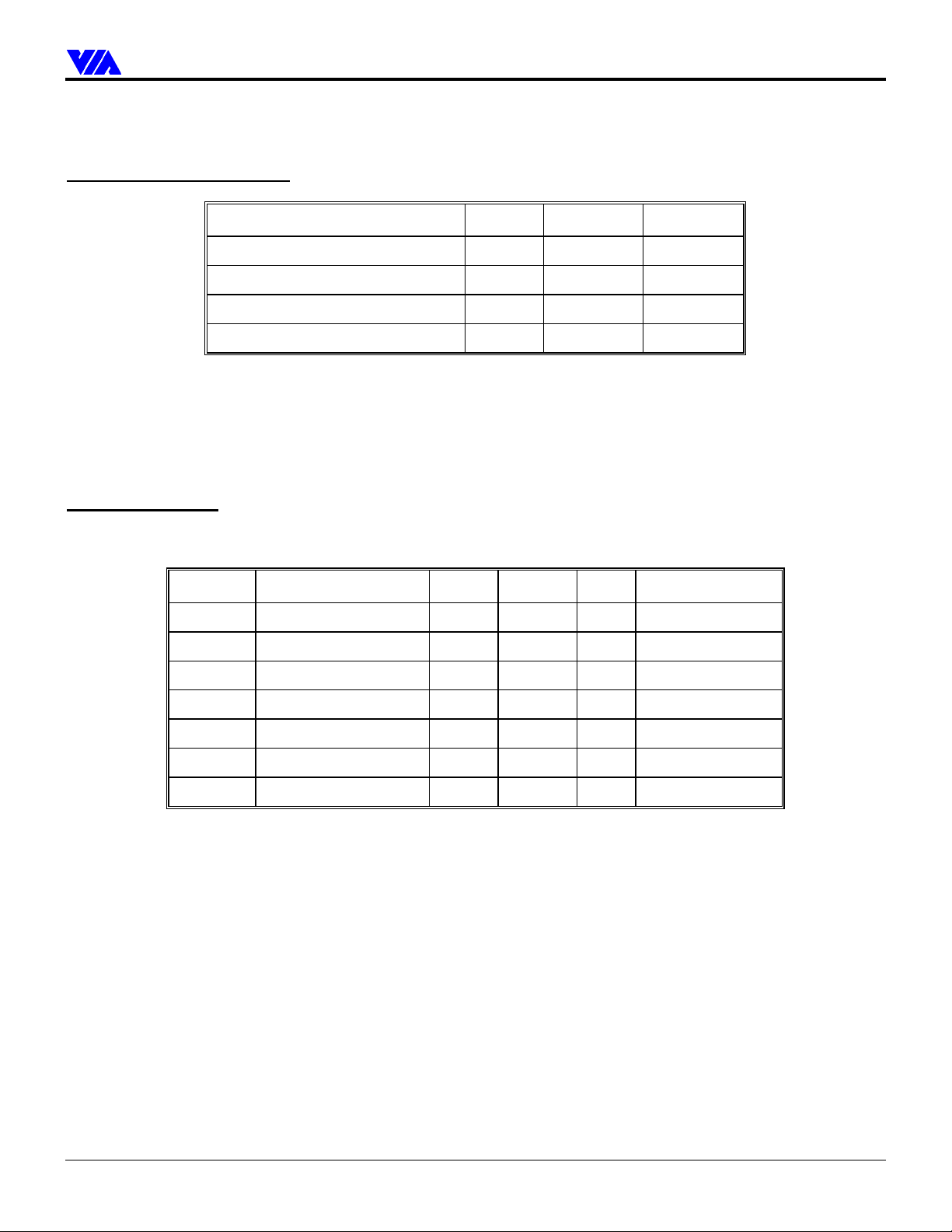
Technologies, Inc.
We ConnectWe Connect
Absolute Maximum Ratings
Parameter Min Max Unit
Ambient operating temperature 0 70
Storage temperature -55 125
Input voltage -0.5 5.5 Volts
ELECTRICAL SPECIFICATIONS
o
C
o
C
Output voltage (VCC = 3.1 - 3.6V) -0.5 V
Note: Stress above the conditions listed may cause permanent damage to the
device. Functional operation of this device should be restricted to the
conditions described under operating conditions.
DC Characteristics
TA-0-70oC, VCC=3.3V+/-5%, GND=0V
Symbol Parameter Min Max Unit Condition
V
IL
V
IH
V
OL
V
OH
I
IL
I
OZ
Input low voltage -0.50 0.8 V
Input high voltage 2.0 VCC+0.5 V
Output low voltage - 0.45 V IOL=4.0mA
Output high voltage 2.4 - V IOH=-1.0mA
Input leakage current - +/-10 uA 0<VIN<V
Tristate leakage current - +/-20 uA 0.45<V
+ 0.5 Volts
CC
CC
OUT<VCC
I
CC
Power supply current - TBD mA
Revision 0.2 March 10, 2000 -29- Electrical Specifications
Page 35
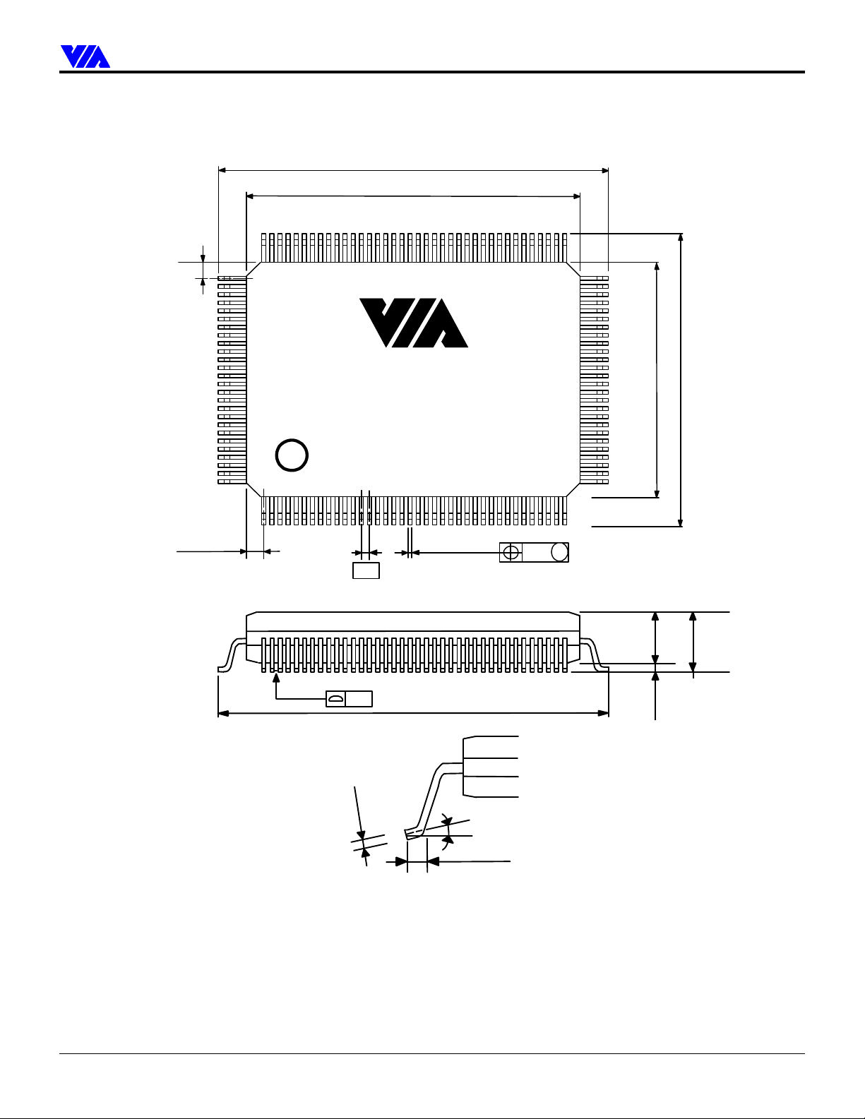
Technologies, Inc.
We ConnectWe Connect
PACKAGE MECHANICAL SPECIFICATIONS
23.2 +/-0.2
20.0 +/-0.2
0.75TYP
128
0.75TYP
103
102
1
VT6305
YYWWVV TAIWAN
LLRLLLLLL ©
0.2 +/-0.03
0.5
65
64
17.2 +/-0.2
14.0 +/-0.2
M
39
38
0.08
M
2.72
+0.18
-0.22
3.40
Max
0.1
0.15
23.2+/-0.2
+0.1
-0.05
0~10
o
0.25
Min
0.5+/-0.2
Figure 4. Mechanical Specifications – 128 Pin PQFP Package
Revision 0.2 March 10, 2000 -30- Package Mechanical Specifications
 Loading...