

Page 1

VIA Technologies, Inc. Preliminary VT6516 Datasheet
VT6516
16/12-PORT 10/100BASE-T/TX
ETHERNET SWITCH CONTROLLER
REVISION ‘E’ DATASHEET
(Preliminary)
ISSUE 1: July 31, 1999
VIA Technologies, Inc.
1
Page 2

VIA Technologies, Inc. Preliminary VT6516 Datasheet
PRELIMINARY RELEASE
Please contact VIA Technologies for the latest documentation.
Copyright Notice:
Copyright © 1995, VIA Technologies Incorporated. Printed in Taiwan. ALL RIGHTS
RESERVED.
No part of this document may be reproduced, transmitted, transcribed, stored in a retrieval
system, or translated into any language, in any form or by any means, electronic, mechanical,
magnetic, optical, chemical, manual or otherwise without the prior written permission of VIA
Technologies Incorporated.
The VT86C100P may only be used to identify products of VIA Technologies.
All trademarks are the properties of their respective owners.
Disclaimer Notice:
No license is granted, implied or otherwise, under any patent or patent rights of VIA
Technologies. VIA Technologies makes no warranties, implied or otherwise, in regard to this
document and to the products described in this document. The information provided by this
document is believed to be accurate and reliable to the publication date of this document.
However, VIA Technologies assumes no responsibility for any errors in this document.
Furthermore, VIA Technologies assumes no responsibility for the use or misuse of the
information in this document and for any patent infringements that may arise from the use of
this document. The information and product specifications within this document are subject to
change at any time, without notice and without obligation to notify any person of such change.
Offices:
1045 Mission Court 8th Floor, No. 533
Fremont, CA 94539 Chung-Cheng Rd., Hsin-Tien
USA Taipei, Taiwan ROC
Tel: (510) 683-3300 Tel: (886-2) 2218-5452
Fax: (510) 683-3301 Fax: (886-2) 2218-5453
Online Services:
BBS : 886-2-2186408
FTP : FTP.VIA.COM.TW
HTTP:WWW.VIA.COM.TW –or- WWW.VIATECH.COM
2
Page 3

VIA Technologies, Inc. Preliminary VT6516 Datasheet
TABLE OF CONTENTS
TABLE OF CONTENTS................................................................................................................................3
FIGURES AND TABLES ...............................................................................................................................4
REVERSION HISTORY ................................................................................................................................5
FEATURES ................................................................................................................................................6
BLOCK DIAGRAM...................................................................................................................................... 9
BALL OUT DIAGRAM............................................................................................................................... 11
RMII-mode Ball out Diagram ........................................................................................................... 11
MII-mode Ballout Diagram............................................................................................................... 12
LOGIC SYMBOL ...................................................................................................................................... 13
PIN DESCRIPTIONS.................................................................................................................................. 14
JUMPER STRAPPING................................................................................................................................. 18
SECTION I FUNCTIONAL DESCRIPTIONS ...................................................................................... 19
1. GENERAL DESCRIPTION ...................................................................................................................... 19
2. THE VIA ETHER SWITCH ARCHITECTURE............................................................................................ 19
2.1 Switch initialization procedures .................................................................................................. 19
2.2 Packet receiving and forwarding follow .......................................
3. INTERFACE DESCRIPTIONS................................................................................................................... 20
3.1 Buffer Memory (SDRAM) Interface and Table (SRAM) interface..
4. FUNCTIONAL DESCRIPTION ................................................................................................................. 33
4.1 Packet Reception and Address recognition.................................................................................. 33
4.2 Packet Forwarding and VLAN..................................................................................................... 33
4.3 Network Management Features................................................................................................... 34
¿ù»~! ©|¥¼©w¸q®ÑÅÒ¡C
¿ù»~! ©|¥¼©w¸q®ÑÅÒ¡C
SECTION II REGISTER MAP...............................................................................................................36
1. REGISTER TABLES ............................................................................................................................. 36
2 CPU INTERFACE REGISTERS MAP......................................................................................................... 36
3 SWITCH INTERNAL REGISTERS MAP..................................................................................................... 37
4. DETAIL OF SWITCH REGISTER.............................................................................................................. 44
4.1 Registers of SDRAM Control Module ......................................................................................... 44
4.2 Registers of SRAM Control Module............................................................................................ 46
4.4 Registers of Buffer Control Module............................................................................................. 48
4.5 Registers of Forwarding Control Module................................................................................... 49
4.6 Registers of PHY Control Module .............................................................................................. 53
4.7 Registers of EEPROM Control Module....................................................................................... 55
4.8 Registers of CPU Interface Module ............................................................................................. 56
4.9 Registers of MAC/IO Control Module......................................................................................... 59
4.10 Registers of CPU IO Control Module....................................................................................... 63
SECTION III ELECTRICAL SPECIFICATIONS.................................................................................65
ABSOLUTE MAXIMUM RATINGS............................................................................................................... 65
DC CHARACTERISTICS............................................................................................................................ 65
AC CHARACTERISTICS............................................................................................................................ 65
PACKAGE MECHANICAL SPECIFICATIONS................................................................................................. 73
3
Page 4

VIA Technologies, Inc. Preliminary VT6516 Datasheet
FIGURES AND TABLES
Figure 1: Block Diagram .............................................................................................9
Figure 3-3 .................................................................................................................22
Figure 3-6: Algorithm of Initialization of Free Link Lists. ..........................................22
Figure 3-1 SRAM......................................................................................................26
Figure 3-2 Free buffer link structure ..........................................................................27
Table 1-0 Free buffer link structure............................................................................27
Figure 3-5 The Address table entries structure +........................................................27
Table 1-1 Address table structure ..............................................................................28
Table 3-1 RMII interface signals ................................................................................30
Figure 3-1 RMII timing diagram................................................................................30
Table 3-2 MII interface signals ..................................................................................31
Figure 3-2 MII timing diagram .................................................................................. 31
4
Page 5
VIA Technologies, Inc. Preliminary VT6516 Datasheet
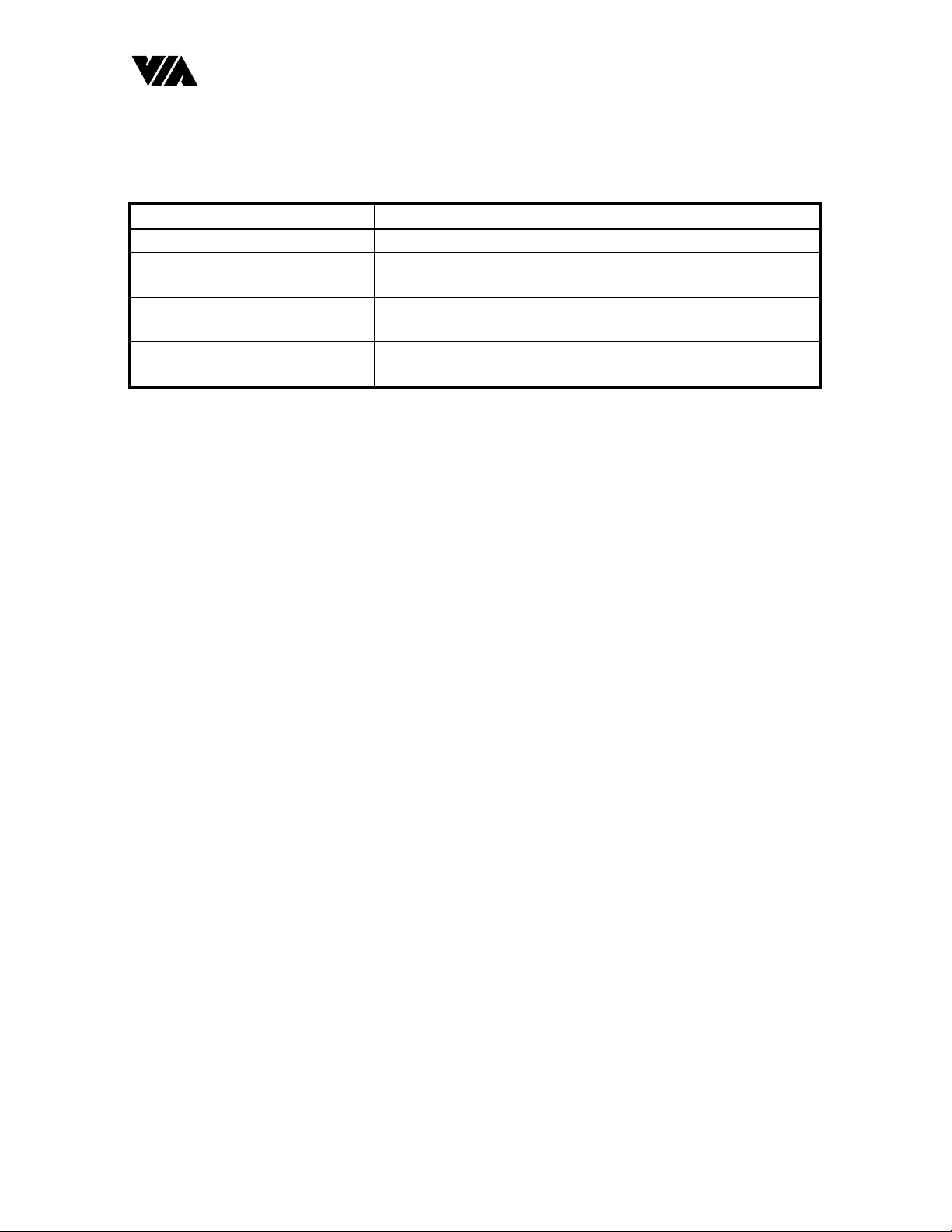
REVERSION HISTORY
Reversion Date Reason for change By
V0.90 2/18/1999 First release version JeffreyChang
V0.91 6/2/1999 Add D version silicon features
modification
V0.92 8/23/1999 Add E version silicon features
modification
V0.93 9/9/1999 Revision according to Weipin’s,
Kevin’s, and Ruth’ s comments
JeffreyChang
MurphyChen
MurphyChen
5
Page 6

VIA Technologies, Inc. Preliminary VT6516 Datasheet
FEATURES
l Single chip 16/12 ports 10/100M Ethernet switch controller
- Highly integrated single chip shared memory switch engine
- With option for 16 RMII (Reduced Media Independent Interface) ports or 12 MII
(Media Independent Interface) ports
- Non-blocking layer 2 switch, 148,810 packets/sec on each 100Mbps Ethernet port
l Media Access Control (MAC)
- Dual 192-bytes FIFO’s of receive and transmit for each port
- CRC generator for outgoing packets from CPU port
- IEEE 802.3X compliant flow control for full duplex ports
- Backpressure for half duplex ports
l Two switching mechanisms
- Supports ‘store and forward’ switching without forwarding CRC-bad packets
- Supports ‘cut through’ switching subject to long packets of length over 290 bytes for
100Mbps ports or of length over 98 bytes for 10Mbps ports
l Packet buffering
- Glueless 64-bit interface to SDRAM as a packet buffer pool with size from 2M bytes
(SGRAM) to 512 M bytes
- 1536 bytes for each packet buffer
l External 32 bits SSRAM interface for forwarding table and memory link table
- Link list structure initialized by software
- 2K up to 32K unicast/multicast addresses table entries with VLAN information
- Supports static entries for upper-layer multicast protocols, e.g. IGMP
l Advanced address recognition
- Layer 2 MAC address recognition engine to enable wire-speed forwarding rate
- Self learning mechanism
- Supports multiple MAC address per-port from 2K up to 32K unicast/multicast
addresses
l Switch management support
- Supports port mirroring (Sniffer feature)
- Supports spanning tree algorithm
- Supports CPU direct access to SDRAM and SSRAM
- Supports five statistical counters in each port
l Supports I
l Support port-grouping VLAN
- Configurable server ports belonging to multiple VLAN groups
l Support port-based trunking
- Three types of trunk grouping: one trunk group with 2 or 4 ports, two trunk groups
each with 2 ports
- Load balance according to MAC address and port number
l CPU interface VIA 8/16 bits ISA-like interface
2
C EEPROM interface for customized configuration
6
Page 7

VIA Technologies, Inc. Preliminary VT6516 Datasheet
- Chip initialization, auto-aging and spanning tree algorithm support by firmware
- Auto-sensing 10/100M media speed, duplex mode, and flow-control capability by
firmware
l 50MHz internal reference clock rate
l 50~100MHz SDRAM clock rate, typically 83MHz
l 50~100MHz SSRAM clock rate, typically 83MHz
l Single +3.3V supply, 0.3µm standard CMOS technology
l 476 ball BGA package
7
Page 8

Page 9
VIA Technologies, Inc. Preliminary VT6516 Datarsheet
BLOCK DIAGRAM
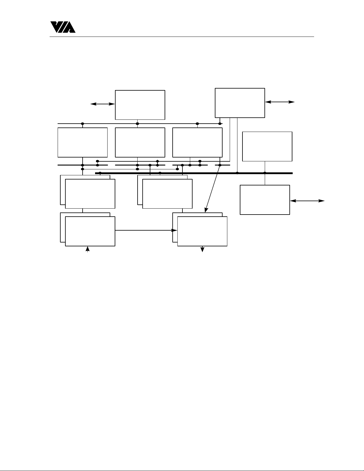
forwarding
control
input
control
RMAC
SRAM
control
buffer
control
output
control
queue
control
TMAC
CPU
interface
scheduler
SDRAM
control
Figure 1: Block Diagram
99/12/09 9
Page 10

Page 11
VIA Technologies, Inc. Preliminary VT6516 Datarsheet
BALL OUT DIAGRAM
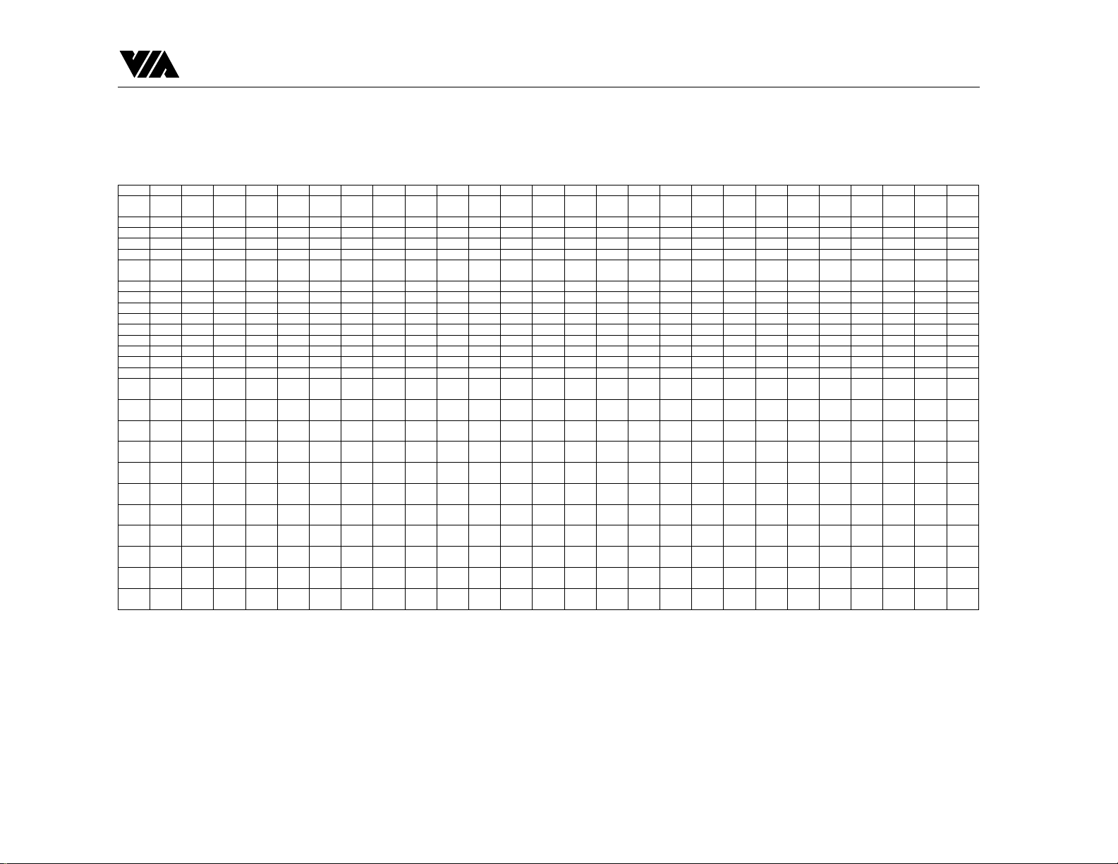
RMII-mode Ball out Diagram
1 2 3 4 5 6 7 8 9 10 11 12 13 14 15 16 17 18 19 20 21 22 23 24 25 26
CSDV2 CRS.DV1RXD1.1 TXEN1 TXD1.0 RXD0.0 MD1 MD3 MD5 MD7 MD9 MD11 MD45 MD47 RAS0 MA3 MA7 MA11 DCS2 DWE0 MD49 MD20 MD22 MD24 MD57 MD58
A
RXD1.2 TXD1.2 TXD1.1 RXD0.1 CSDV0 TXD0.0 MD32 MD34 MD36 MD38 MD40 MD42 MD14 CAS1 MA0 MA4 MA8 BA0 DCS1 DWE1 MD18 MD52 MD54 MD56 MD26 MD27
B
TXEN2 RXD0.2 TXD0.2 TXD0.1 TXEN0 RXD1.0 MD0 MD2 MD4 MD6 MD8 MD10 MD46 CAS0 MA1 MA5 MA9 BA1 DCS0 MD16 MD50 MD21 MD23 MD25 MD59 MD28
C
TXD1.3 CSDV3 TXEN3 NC NC NC MD33 GND MD37 MD39 MD41 MD43 MD13 MD15 RAS1 MA2 MA6 MA10 DCS3 MD48 MD19 MD53 MD55 MD60 MD29 MD61
D
RXD0.3 TXD0.3 RXD1.3 NC VDDI GNDI GND MD35 VDD VDD VDD MD12 MD44 GND GND GND VDD VDD VDD MD17 MD51 GNDI DCLK MD30 MD62 MD31
E
RXD1.4 TXD0.4 RXD0.4 TXEN4 RCLK50VDDI GND NC NC GND GNDI VDDI MD63 SD16 SD17 SD18
F
RXD0.5 CSDV4 TXD1.4 TXEN5 VDD GND GND SCLK SD19 SD20 SD21 SD22
G
TXD1.5 RXD1.5 TXD0.5 NC VDD VDD NC SD23 SD24 SD25 SD26 SD27
H
TXD0.6 RXD0.6 CSDV5 NC VDD VDD SD31 SD28 SD29 SD30
J
CSDV6 TXD1.6 RXD1.6 TXEN6 NC VDD SA4 SA6 SA7 SA5
K
RXD1.7 TXD0.7 RXD0.7 NC GND GND GND GND GND GND GND VDD SA3 SA2 SA13 SA0
L
CSRV7 TXD1.7 TXEN7 NC GND GND GND GND GND GND GND SA10 SA11 SA12 SA13 SA14
M
RXD1.8 TXD1.8 CSDV8 TXEN8 NC GND GND GND GND GND GND SA15 SA16 SA17 SA9 SA8
N
TXD0.8 RXD0.8 CSDV9 TXEN9 NC GND GND GND GND GND GND GND SD0 SD3 SD2 SD18
P
TXD1.9 RXD1.9 TXD0.9 NC VDD GND GND GND GND GND GND GND SD4 SD7 SD6 SD5
R
RXD0.9 RXD0.10TXD0.10TXEN10VDD GND GND GND GND GND GND SD11 SD12 SD10 SD9 SD8
T
RXD1.10TXD1.10CSDV10NC VDD VPP SADS# SD15 SD14 SD13
U
RXD0.11TXD0.11RXD1.11TXEN11VDD VPP SOE# SCS1# SCS0# SWE#
V
TXD1.11CSDV11RXD0.12TXEN12NC GND GND SCS3# SCS2# HA0 HCS# SCS4#
W
TXD0.12RXD1.12TXD1.12NC GND GNDI GNDI HCLK HD15 INTRQ HA1 HA2
Y
CSDV12RXD0.13TXD0.13NC GNDI VDDI VDD VDD GND GND GND GNDI HD1 HD0 IOW# IOR#
AA
RXD1.13TXEN13TXD1.13NC VDDI VDD VDD NC VPP VPP NC NC GND GND NC NC VPP VPP VPP TEST12 VDDI GND HD3 HD13 HD2 HD14
AB
CSDV13CSDV14TXD1.14NC EEC NC NC NC NC NC NC NC NC NC NC NC NC NC TEST7 TEST11 TEST16 TEST17 HD5 HD11 HD4 HD12
AC
RXD1.14TXD0.14RXD1.15TXEN15EEIO NC NC NC NC NC NC NC NC NC NC NC NC TEST3 TEST6 TEST10 TEST15 TEST20 TEST23 HD9 HD6 HD10
AD
RXD0.14CSDV15TXD0.15MDC NC NC NC NC NC NC NC NC NC NC NC NC NC TEST2 TEST5 TEST9 TEST14 TEST19 TEST22 TEST25 HD8 HD7
AE
TXEN14TXD1.15RXD0.15MDIO NC NC NC NC NC NC NC NC NC NC NC NC NC TEST1 TEST4 TEST8 TEST13 TEST18 TEST21 TEST24 TEST26 RESET
AF
#
99/12/09 11
Page 12

VIA Technologies, Inc. Preliminary VT6516 Datarsheet
MII-mode Ballout Diagram
1 2 3 4 5 6 7 8 9 10 11 12 13 14 15 16 17 18 19 20 21 22 23 24 25 26
CRS1 RXD3_0COL0 TXD1_0RXD0_0MD1 MD32 MD34 MD36 MD38 MD40 MD42 MD14 CAS1# MA0 MA4 MA8 BA0 DCS1# DWE1# MD18 MD20 MD22 MD24 MD57 MD58
A
RXD1_1RXDV0 TXD3_0RXD2_0CRS0 TXD0_0MD0 MD2 MD4 MD6 MD8 MD10 MD46 CAS0# MA1 MA5 MA9 BA1 DCS0# MD16 MD50 MD52 MD54 MD56 MD26 MD27
B
TXEN1 TXD1_1TXD0_1TXD2_0TXEN0 RXD1_0MD33 MD35 MD37 MD39 MD41 MD43 MD13 MD15 RAS1# MA2 MA6 MA10 DCS3# MD48 MD19 MD21 MD23 MD25 MD59 MD28
C
TXD3_1RXD0_1COL1 NC NC NC MD3 VSS MD7 MD9 MD11 MD12 MD44 RAS0# MA3 MA7 MA11 DCS2# DWE0# MD17 MD51 MD53 MD55 MD60 MD29 MD61
D
RXD2_1RXDV1 RXD3_1NC VDD GND VSS MD5 VCC VCC VCC MD45 MD47 VSS VSS VSS VCC VCC VCC MD49 NC GND DCLK MD30 MD62 MD31
E
RXD1_2TXD2_1RXD0_2TXEN2 RCLK50VDD VSS NC NC VSS GND VDD MD63 SD16 SD17 SD18
F
RXD2_2TXD0_2TXD1_2COL2 VCC VSS VSS SCLK SD19 SD20 SD21 SD22
G
TXD3_2CRS2 TXD2_2RCLK2 VCC VCC NC SD23 SD24 SD25 SD26 SD27
H
TXD0_3RXD3_2RXDV2 TCLK2 VCC VCC SD31 SD28 SD29 SD30
J
RXD0_3CRS3 TXD1_3RXD1_3TXEN3 VCC SA4 SA6 SA7 SA5
K
RXD3_3TXD2_3RXD2_3RCLK3 VSS VSS VSS VSS VSS VSS VSS VCC SA3 SA2 SA1 SA0
L
RXDV3 TXD3_3COL3 TCLK3 VSS VSS VSS VSS VSS VSS VSS SA10 SA11 SA12 SA13 SA14
M
TXD0_4RXD1_4TXD1_4CRS4 TXEN4 VSS VSS VSS VSS VSS VSS SA15 SA16 SA17 SA9 SA8
N
TXD3_4RXD0_4RXDV4 COL4 RCLK4 VSS VSS VSS VSS VSS VSS VSS SD0 SD3 SD2 SD1
P
RXD2_4RXD3_4TXD2_4TCLK4 VCC VSS VSS VSS VSS VSS VSS VSS SD4 SD7 SD6 SD5
R
RXD1_5RXD0_5TXD0_5TXEN5 VCC VSS VSS VSS VSS VSS VSS SD11 SD12 SD10 SD9 SD8
T
RXD2_5TXD1_5CRS5 TCLK5 VCC VCC SADS# SD15 SD14 SD13
U
TXD3_5TXD2_5RXD3_5COL5 VCC VCC SOE# SCS1# SCS0# SWE#
V
TXD0_6RXDV5 RXD0_6TXEN6 RCLK5 VSS VSS SCS3# SCS2# HA0 HCS# SCS4#
W
CRS6 RXD1_6TXD1_6TCLK6 VSS GND GND HCLK HD15 INTRQ#HA1 HA2
Y
RXD3_6RXD2_6TXD2_6RCLK6 GND VDD VCC VCC VSS VSS VSS GND HD1 HD0 IOW# IOR#
AA
RXDV6 COL6 TXD3_6TCLK7 VDD VCC VCC NC VCC VCC TCLK9 RXD3_10VSS VSS CRS10 RCLK11VCC VCC VCC TEST12 VDD VSS HD3 HD13 HD2 HD14
AB
RXD1_7CRS7 TXD1_7RCLK7 EEC RCLK8 TCLK8 RXD3_9RXD2_9RCLK9 TXD2_9RXD2_10RCLK10TCLK10RXD3_11RXDV11TCLK11CRS11 TEST7 TEST11 TEST16 TEST17 HD5 HD11 HD4 HD12
AC
RXD0_7TXD0_7RXD3_7COL7 EEIO RXD0_8TXD0_8TXD3_8RXD1_9TXEN9 TXD3_9RXD1_10TXEN10TXD2_10RXD2_11TXEN11TXD2_11TEST3 TEST6 TEST10 TEST15 TEST20 TEST23 HD9 HD6 HD10
AD
TXEN7 RXDV7 TXD2_7MDC RXD2_8RXDV8 TXD1_8COL8 RXD0_9TXD0_9COL9 RXD0_10TXD0_10TXD3_10RXD1_11TXD0_11TXD3_11TEST2 TEST5 TEST9 TEST14 TEST19 TEST22 TEST25 HD8 HD7
AE
TXD3_7RXD2_7MDIO RXD3_8RXD1_8TXEN8 TXD2_8CRS8 RXDV9 TXD1_9CRS9 RXDV10TXD1_10COL10 RXD0_11TXD1_11COL11 TEST1 TEST4 TEST8 TEST13 TEST18 TEST21 TEST24 TEST26 RESET
AF
#
99/12/09 12
Page 13
VIA Technologies, Inc. Preliminary VT6516 Datarsheet
LOGIC SYMBOL
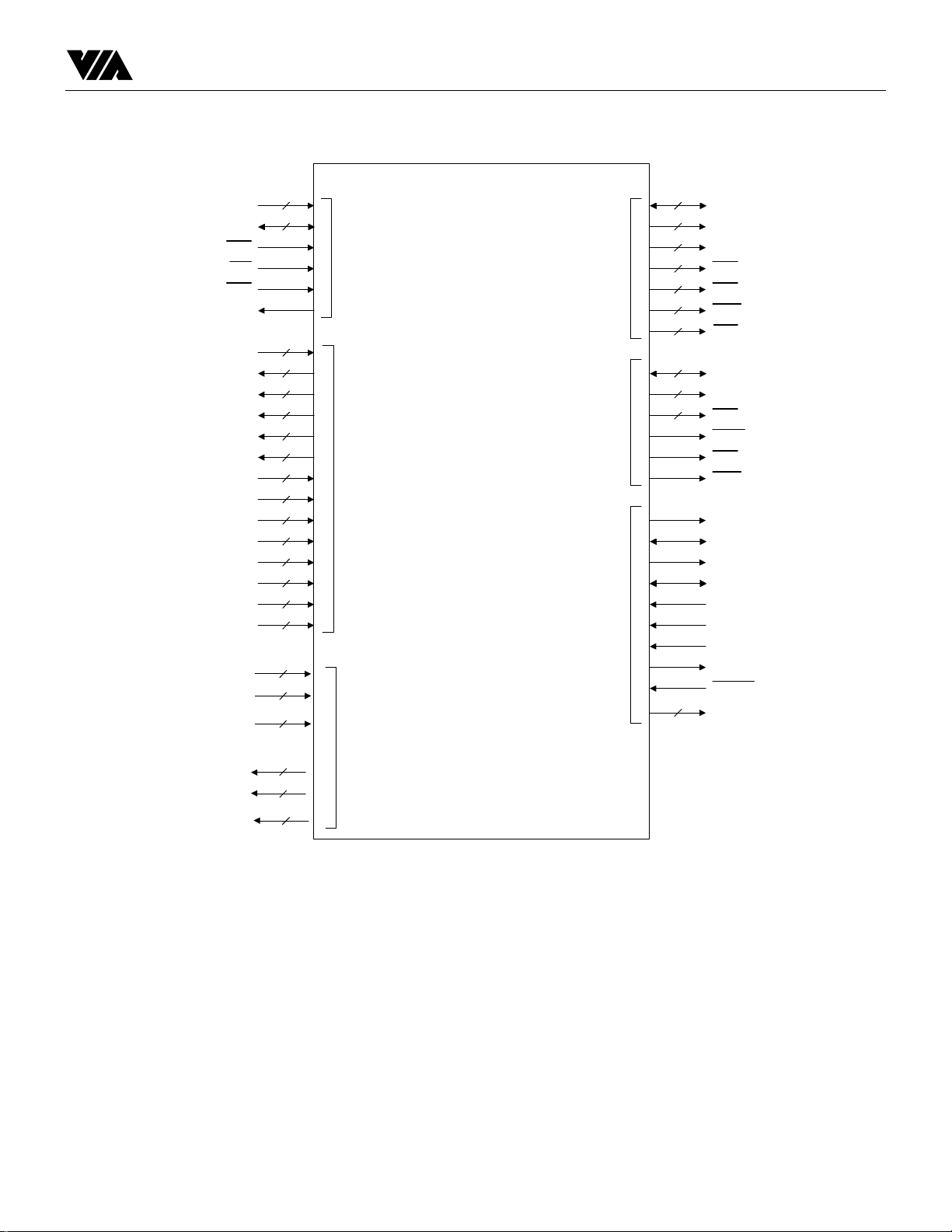
HA[2:0]
HD[15:0]
HCS
IOR
IOW
INTRQ
TCLK[11:0]
TXD0[11:0]
TXD1[11:0]
TXD2[11:0]
TXD3[11:0]
TXEN[11:0]
COL[11:0]
CRS[11:0]
RXD0[11:0]
RXD1[11:0]
RXD2[11:0]
RXD3[11:0]
RCLK[11:0]
RXDV[11:0]
CRS_DV[15:0]
RXD0[15:0]
RXD1[15:0]
TXEN[15:0]
TXD0[15:0]
TXD1[15:0]
16
16
16
16
16
16
12
12
12
12
12
12
12
12
12
12
12
12
12
12
16
3
HOST
Interface
MII
Interface
RMII
Interface
VT6516
Miscellaneous
Interface
SDRAM
Interface
SRAM
Interface
64
12
32
18
26
2
2
2
2
4
5
MD[63:0]
MA[11:0]
BA[1:0]
RAS[1:0]
CAS[1:0]
DWE[1:0]
DCS[3:0]
SD[31:0]
SA[17:0]
SCS[4:0]
SADS
SOE
SWE
EEC
EEIO
MDC
MDIO
RCLK50
DCLK
SCLK
HCLK
RESET
TEST[26:1]
-13-
Page 14
VIA Technologies, Inc. Preliminary VT6516 Datarsheet
RAS
RAS
RAS
CAS
CAS
CAS
DWE
DCS
SCS
SADS
SOE
SWE
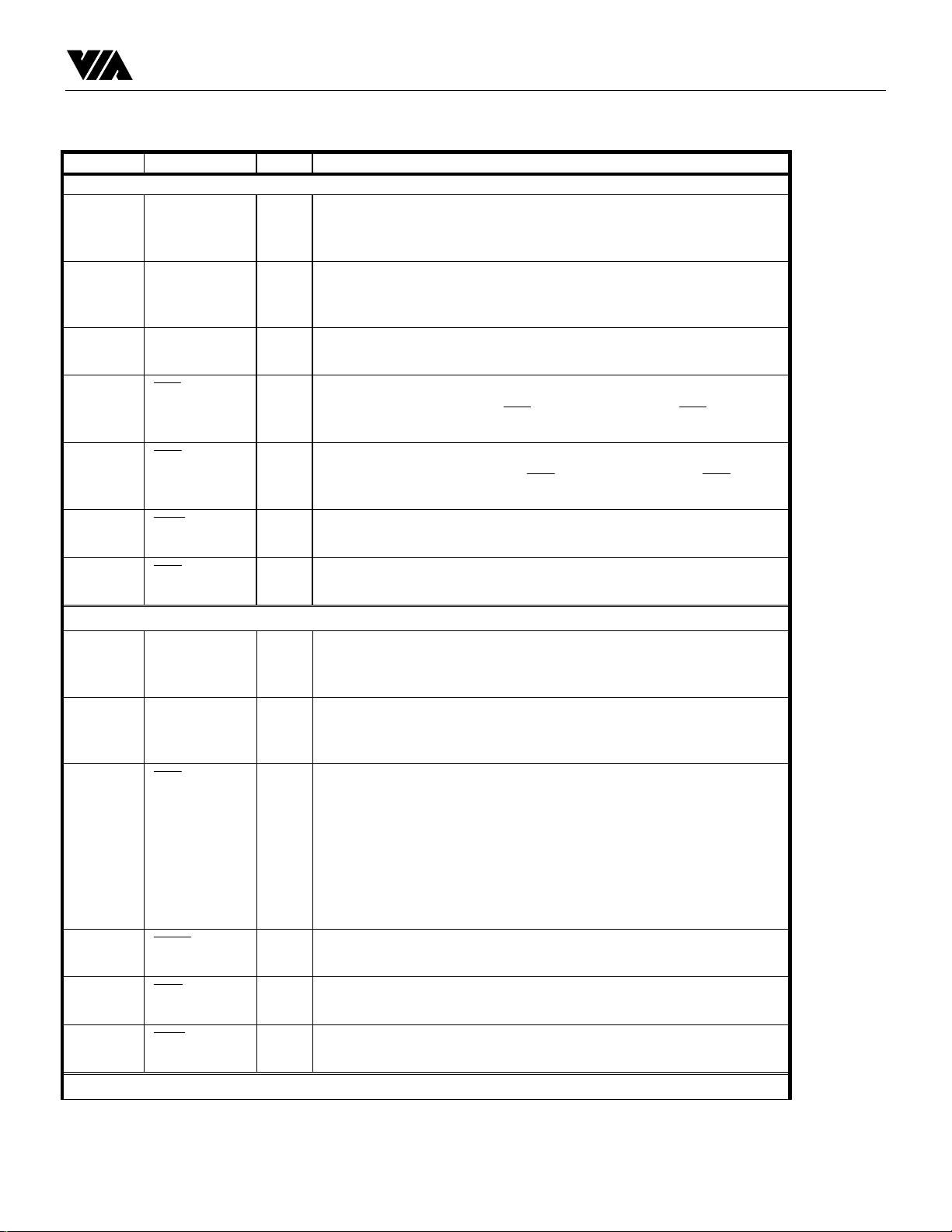
PIN DESCRIPTIONS
No. Name Type Description
SDRAM Interface
See Ball
Table
See Ball
Table
See Ball
Table
MD[63:0] I/O
MA[11:0] O
BA[1:0] O
SDRAM Data:
64-bit SDRAM data bus. These signals connect directly to the data
input/output pins of the SDRAM devices.
SDRAM Address Bus:
12-bit SDRAM data bus. These signals connect directly to the address
input of the SDRAM devices.
Bank Identifier for Bank 0 and 1:
See Ball
Table
See Ball
Table
See Ball
Table
See Ball
Table
See Ball
Table
See Ball
Table
See Ball
Table
See Ball
Table
[1:0]
[1:0]
[1:0]
[3:0]
SD[31:0] I/O
SA[17:0] O
[4:0]
[1:0]
O
O
O
O
O
O
Row Address Strobes for Bank 0 and 1:
DRAM row address strobes.
for Bank 1.
Column Address Strobes for Bank 0 and 1:
DRAM column address strobes.
used for Bank 1.
DRAM Write Enable for Bank 0 and 1:
DRAM Chip Select:
VT-3061A supports at most 4 SDRAM DIMM modules.
SRAM Interface
SRAM Data:
32-bit SRAM data bus. These signals connect directly to the data
input/output pins of the SRAM devices.
SRAM Address Bus:
18-bit SDRAM data bus. These signals connect directly to the address
input of the SDRAM devices.
SRAM Chip Select:
SRAM Type Chip Select Pins Address Pins
---------------- ---------------------- -----------------32KBx32 SCS[0] & SA[15] SA[14:0]
64KBx32 SCS[0] & SA[16] SA[15:0]
128KBx32 SCS[0] & SA[17] SA[16:0]
256KBx32 SCS[0] SA[17:0]
Synchronous Processor Address Status
[0] is used for Bank 0.
[0] is used for Bank 0.
[1] is used
[1] is
See Ball
Table
See Ball
Table
[1:0]
[1:0]
O
Output Enable
O
SRAM Write Enable:
Miscellaneous Interface
-14-
Page 15
VIA Technologies, Inc. Preliminary VT6516 Datarsheet
RESET
See Ball
Table
See Ball
Table
See Ball
Table
See Ball
Table
See Ball
Table
See Ball
Table
See Ball
Table
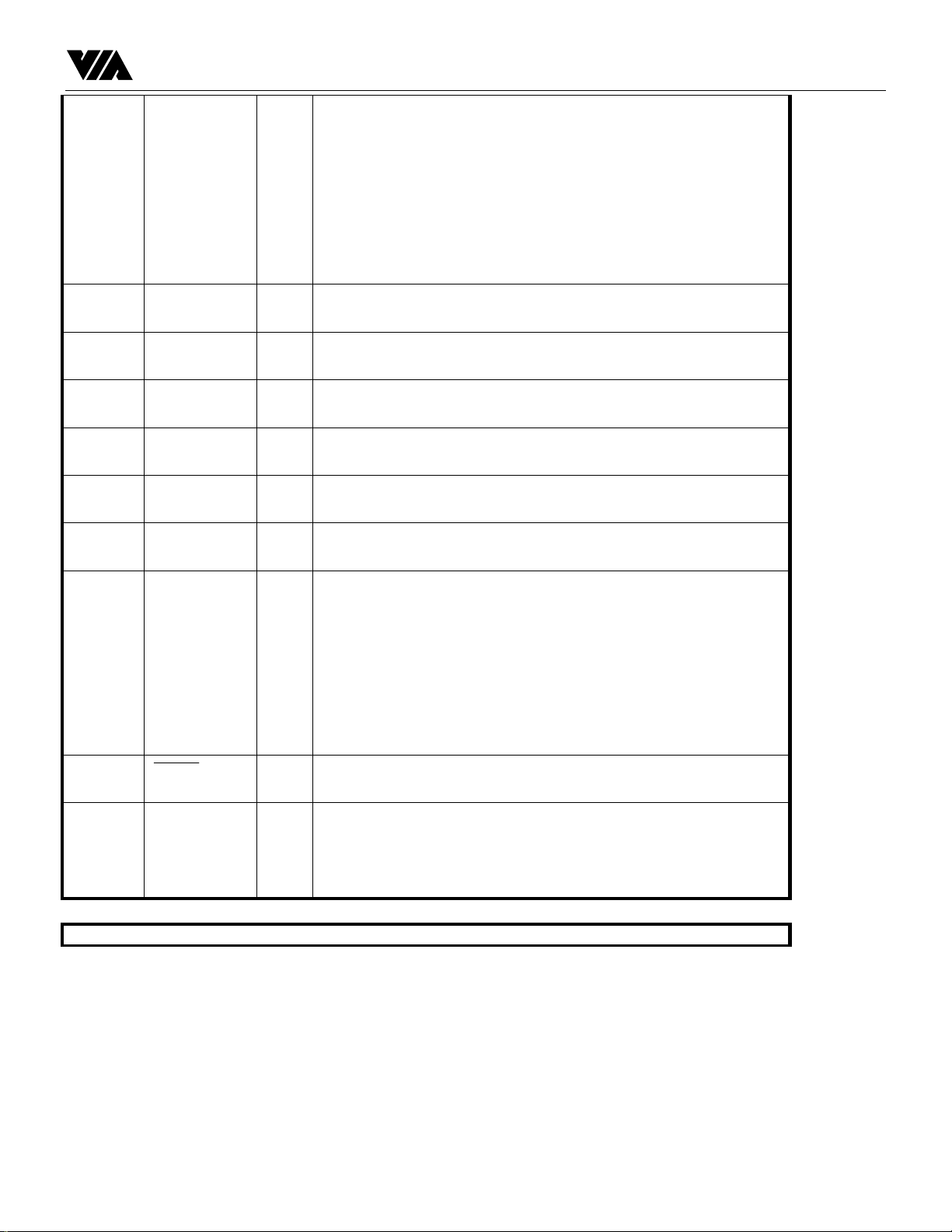
EEC O
EEIO I/O
MDC O
MDIO I/O
RCLK50 I
DCLK I
SCLK I
Serial EEPROM Interface Clock Output:
EEPROM Device Addressing in the demo board:
PAGE 0 (EEPROM): Device Address = 1010 000 XXXXXXXX
PAGE 1 (EEPROM): Device Address = 1010 001 XXXXXXXX
PAGE 2 (EEPROM): Device Address = 1010 010 XXXXXXXX
PAGE 3 (EEPROM): Device Address = 1010 011 XXXXXXXX
PAGE 4 (SDRAM BANK-0): Device Address = 1010 100 XXXXXXXX
PAGE 5 (SDRAM BANK-1): Device Address = 1010 101 XXXXXXXX
Serial EEPROM Interface Data I/O
Management Interface (MI) Clock Output
Management Interface (MI) Data I/O
Main Reference Clock:
SDRAM Reference Clock:
SRAM Reference Clock
See Ball
Table
See Ball
Table
See Ball
Table
HCLK O
SYSLED[26:0
]
HOST Reference Clock
HCLK is determined by the strapping pins in SYSLED[3:1], i.e. the jump
selection of J1[5-6, 3-4, 1-2]:
J1[OFF,OFF,OFF] => 8MHz
J1[ OFF,OFF, ON] => 16MHz
J1[OFF, ON, OFF] => 25MHz
J1[OFF, ON, ON] => 4MHz
J1[ ON,OFF,OFF] => 33MHz
I
SYSTEM RESET
O
SYSTEM Output Pins for LED:
SYSLED[8:0] are connected to pull-up IO PADs for strapping.
SYSLED[25:9] are connected to IO PADs without pull up/down.
All SYSLED[25:0] are
HOST Interface
-15-
Page 16
VIA Technologies, Inc. Preliminary VT6516 Datarsheet
HCS
HCS
IOR
IOR
IOW
IOW
See Ball
Table
See Ball
Table
See Ball
Table
See Ball
Table
See Ball
Table
See Ball
Table
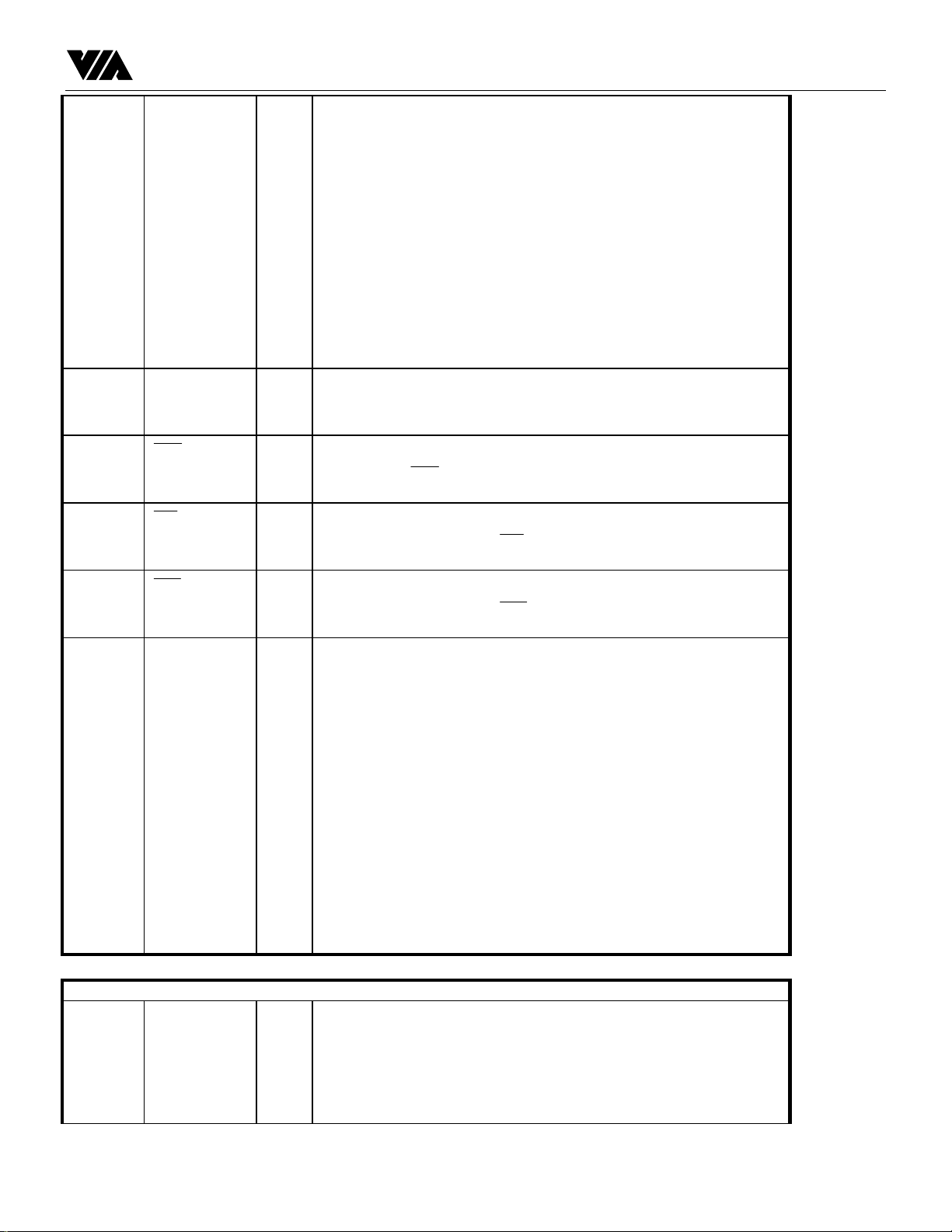
HA[2:0] I
HD[15:0] I/O
I
I
I
INTRQ O
HOST IDE-Interface Address Bus:
3’b000: command the switch that the whole 16-bit data in the HOST data
bus HD[15:0] is valid for packet-data read/write.
3’b001: command the switch that only the 8-bit data in the HOST data bus
HD[15:0] is valid for internal registers read/write.
3’b010: command the switch to write the low byte in the HOST data bus
HD[15:0] into the low byte of the 16-bit switch address register
for internal registers reference.
3’b011: command the switch to write the low byte in the HOST data bus
HD[15:0] into the high byte of the 16-bit switch address register
for internal registers reference.
3’b1xx: bus-idle command. Keep this address bus to be 3’b111 as the
HOST has no access to VT-3061A.
HOST IDE-Interface Data Bus:
The whole 16-bit data bus is valid for packet data read/write. However,
only the 8-bit data bus is valid for internal registers read/write.
HOST Chip Select:
Active LOW.
must be asserted during the access of HOST IDE
interface.
IO READ:
High-to-Low Edge Trigger.
must be asserted from high to low to
begin the read cycle of HOST IDE interface.
IO READ:
High-to-Low Edge Trigger.
must be asserted from high to low to
begin the write cycle of HOST IDE interface.
Interrupt Request:
Connected to the HOST external interrupt pin. It is asserted as the
following four interrupt events happen:
(1) MII Management Registers read/write command done
(2) EEPROM read/write command done
(3) Receiving a packet destined to HOST
(4) Finishing transmission of a packet issued by HOST
The interrupt cause is recorded in register IRQSTS[3:0] in address 2000H.
To clear the individual interrupt, The corresponding register has to be
written:
(1) register CLR_PHY_INT in 1806H for PHY interrupt.
(2) register CLR_EE_INT in 1C04H for EEPROM interrupt.
(3) register CLR_RCV_INT in 6403H for packet-receiving interrupt.
l register CLR_SENT_INT in 6411H for packet-sent interrupt.
MII Interface
See Ball
Table
TCLK[11:0] I
Transmit Clock for Port 0-11:
TCLK is driven by the PHY device. TCLK is a continuous clock that
provides the timing reference for the transfer of the TXEN and TXD
signals to the PHY. A PHY operating at 100Mbps must provide a TCLK
frequency of 25MHz and a PHY operating at 10Mbps must provide a
TCLK frequency of 2.5MHz.
-16-
Page 17
VIA Technologies, Inc. Preliminary VT6516 Datarsheet
See Ball
Table
See Ball
Table
See Ball
Table
See Ball
Table
See Ball
Table
See Ball
Table
See Ball
Table
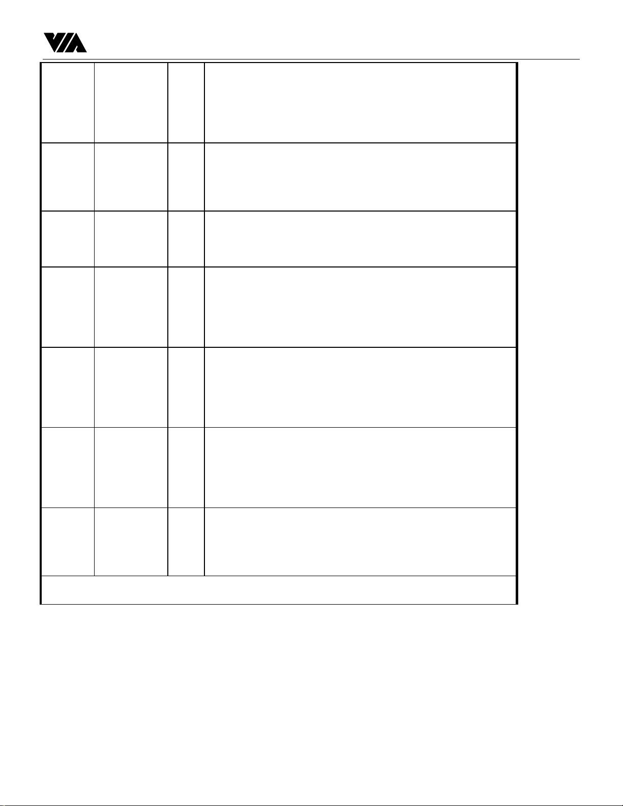
Note: Some flat MII input pin when the VT6516 under the RMII application, please use 22 ohm resister
pull down, refer to Table XXXX
TXD<3:0>[11:0]O
TXEN[11:0] O
COL[11:0] I
CRS[11:0] I
RXD<3:0>[11
:0]
RCLK[11:0] I
RXDV[11:0] I
Transmit Data for Port 0-11:
TXD is a bundle of 4 data signals (TXD<3:0>) that shall transition to the
TCLK. For each TCLK period in which TXEN is asserted, TXD<3:0> are
accepted for transmission by the PHY. TXD<0> is the least significant bit.
While TXEN is de-asserted, TXD<3:0> shall have no effect upon the
PHY, and the value of TXD<3:0> is unspecified.
Transmit Enable for Port 0-11:
TXEN shall transition synchronous to the TCLK. TXEN indicates the
nibbles presenting on the MII for transmission. It shall be asserted
synchronously with the first nibble of the preamble and shall remain
asserted while all nibbles to be transmitted are presented to the MII.
Collision Detected for Port 0-11:
COL shall be asserted by the PHY asynchronously upon detection of a
collision on the medium, and shall remain asserted while the collision
condition persists.
Carrier Sense for Port 0-11:
CRS shall be asserted by the PHY asynchronously upon detection of a
non-idle medium or while TX_EN is asserted. CRS shall be de-asserted by
the PHY asynchronously upon detection of idle conditions on both
transmit and receive media. The PHY shall ensure that CRS remains
asserted throughout the duration of a collision condition.
I
Receive Data for Port 0-11:
RXD is a bundle of 4 data signals (RXD<3:0>) that shall transition to the
RCLK. For each RCLK period in which RXDV is asserted, RXD<3:0>
from the PHY are accepted by the switch’s MAC. RXD<0> is the least
significant bit. While RXDV is de-asserted, RXD<3:0> shall have no
effect upon the switch’s MAC, and the value of RXD<3:0> is unspecified.
Receive Clock for Port 0-11:
RCLK is sourced from the PHY. RCLK is a continuous clock that provides
the timing reference for the transfer of the RXDV and RXD signals from
the PHY. A PHY operating at 100Mbps must provide a RCLK frequency
of 25MHz and a PHY operating at 10Mbps must provide a RCLK
frequency of 2.5MHz.
Receive Data Valid for Port 0-11:
RXDV is driven by the PHY to indicate the nibbles presenting on the MII
for receiving. RXDV shall transition synchronous to the RCLK. It shall be
asserted synchronously with the first nibble of the preamble and shall
remain asserted while all nibbles to be received are presented to the MII.
-17-
Page 18
VIA Technologies, Inc. Preliminary VT6516 Datarsheet
RMII interface
See Ball
Table
See Ball
Table
See Ball
Table
See Ball
Table
See Ball
Table
See Ball
Table
Power Supply & Ground
See Ball
Table
See Ball
Table
CRS_DV[15:0]I Carries sense and data valid from port 15 to port 0 :
RXD0[15:0] I Receive data zero from port 15 to port 0 :
RXD1[15:0] I Receive data one from port 15 to port 0 :
TXEN[15:0] O Transmit enable from port 15 to port 0 :
TXD0[15:0] O Transmit data zero from port 15 to port 0 :
TXD1[15:0] O Transmit data one from port 15 to port 0 :
VDD, VDDA P Positive 3.3V Supply: Supply power to Internal digital logic, Digital I/O
VSS, VSSA G Negative Supply: digital ground. Multiple bonding pads are required to
pads, and TD, TX pads. Double bonding may be required.
separate core and I/O pads ground.
JUMPER STRAPPING
Jumper Pin Description
HOST Clock
J1 [5-6], [3-4], [1-2]SYSLED[3:1]HOST Clock (HCLK) Rate Selection:
J1[OFF,OFF,OFF] (SYSLED[3:1]==3’b111) => 8MHz
J1[ OFF,OFF, ON] (SYSLED[3:1]==3’b110) => 16MHz
J1[OFF, ON, OFF] (SYSLED[3:1]==3’b101) => 25MHz
J1[OFF, ON, ON] (SYSLED[3:1]==3’b100) => 4MHz
J1[ ON,OFF,OFF] (SYSLED[3:1]==3’b011) => 33MHz
PHY Mode
J1 [7-8] SYSLED[4] PHY Device Selection:
J1[OFF] (SYSLED[4]==1’b1) => RMII PHY
J1[ ON] (SYSLED[3:1]==1’b0) => MII PHY
SRAM Type
J1 [11-12,9-10] SYSLED[6:5]SRAM Device Type Selection:
J1[OFF,OFF] (SYSLED[6:5]==2’b11) => 64K x 32 SRAM
J1[OFF,ON] (SYSLED[6:5]==2’b10) => 128K x 32 SRAM
J1[ON,OFF] (SYSLED[6:5]==2’b01) => 32K x 32 SRAM
-18-
Page 19

VIA Technologies, Inc. Preliminary VT6516 Datarsheet
SECTION I FUNCTIONAL DESCRIPTIONS
1. GENERAL DESCRIPTION
The VT6516 is a switch engine chip implementation of a 16 ports 10/100M Ethernet switch system for IEEE
802.3 and IEEE 802.3u network. Each of individual port can be either auto-sensing or manually selected to run
at 10Mbps or 100Mbps speed rate and under full or half duplex mode.
There are sixteen independent MACs within the VT6516 chip. The MAC controller controls the receiving,
transmitting, and deferring of each individual port, and the MAC controller also provides framing, FCS
checking, error handling, status indication and flow control function.
The VT6516 10/100M N-way switch port IC is wire-speed performance and low-cost packet switch; it can
forward up to 148,810 packets/sec on each Ethernet port. The VT6516 support 12 ports MII or 16 ports RMII
(reduce MII) interface for network interface,
The VT6516 used the simple 8/16 bits ISA-like interface to support initiation, expansion and management.
The system CPU can access various registers inside VT6516 through a simple ISA-like CPU interface. The CPU
can configure the switch by writing into the appropriate registers, or retrieve the status of the switch by reading
the corresponding registers. The CPU can also access the register of external transceiver (PHY) device through
the CPU interface.
The VT6516 supports new features including port based VLAN , 802.3X flow control, and the VT6516 also
support the sniffer function to monitor network traffic in special ports.
2. THE VIA ETHER SWITCH ARCHITECTURE
The VT6516 switch engine uses the shared memory architecture. In order to improve the packet latency,
VT6516 provides two methods for packet switching, one is cut-through, another is store-and-forwarding. A
typical packet flow for Ethernet switch is described as follows in 4.5.
2.1 Switch initialization procedures
1. Test all of the on board components except the switch chip or access VIA the switch chip, including UART,
LED, etc.
2. Switch SDRAM test --- switch chip SDRAM control hardware initialization, configuration, SDRAM size
determination (VIA embedded EEPROM in SDRAM module) and read write test.
3. Switch SRAM test --- switch chip SDRAM control hardware initialization and read write test. Note that the
SRAM size determination is VIA strapping.
4. Switch IO registers read write test.
5. Ethernet PHY registers read write test ---- the CPU read/write to PHY devices will go through PHY
control in switch chip. Although they are outside components, but we test them as part of the switch chip.
6. Determine link table size; reset free buffer list pointers of bank 0 and 1; initialize free memory block counter.
Note that permanent buffer management is controlled by allocating bit mask. They will be cleared
automatically in the hardware reset or software reset.
2.2 Packet Switching Flow
1. After the switch microprocessor activates a port during initialization, the input control of that port pre-
allocates one packet buffer from buffer pool. In the beginning, the buffer allocated will be from private buffer
pool, but subsequent buffers may come from either private or public buffer pools.
-19-
Page 20

VIA Technologies, Inc. Preliminary VT6516 Datarsheet
2. When receive MAC (RMAC) receives a packet data from the network interface – either through MII or
reduced MII (RMII) – it packs the data into 16-bit word then passes it to input control. If RMAC detects any
error, it also notifies input control to stop forwarding process.
3. Input control extracts the destination MAC address from incoming data, passes it along to forwarding table
control for forwarding decision. In the mean while, it packs 16-bit words into 64-bit quad-words, and saves
it to an input FIFO before storing the packet data to SDRAM.
4. If the switch is configured to “store and forward” mode, input control queues the packet to the output queue
of the destination port after input control is informed by RMAC that this is a good packet and it stores all
packet data to SDRAM. If the switch is configured to “cut-through” mode, the input control queues the
packet to the output queue of the destination port after enough amount of packet is stored in SDRAM to
prevent output FIFO under-run.
5. After the whole packet is received and FCS is correct, input control pass the source MAC address of the
packet to forwarding table control for address learning.
6. Output control of the outbound port de-queue the packet from output queue, and fetch packet data from
SDRAM and save it into output FIFO. Then it notifies the transmit MAC (TMAC) of the new packet to
transmit.
7. TMAC grabs 16-bit at a time from output control, adds preamble and SFD to the beginning of the packet,
then send them out. Proper deferring is done if necessary to conform to 802.3 standard.
8. After the packet is successfully transmitted, TMAC notifies output control of the successful transmission.
Output control then returns the packet to buffer pool.
3. INTERFACE DESCRIPTIONS
BUFFER MEMORY (SDRAM) INTERFACE AND TABLE (SSRAM) INTERFACE
VT6516 provides a 64-bit SDRAM/SGRAM interface for packet buffering and a 32-bit synchronous SRAM
(SSRAM) interface for maintaining address table and various link lists. VT6516 uses SDRAM as packet buffers.
Each packet buffer is a 1536-byte contiguous memory block in SDRAM, and corresponds to a 12-byte link node
data structure in SSRAM. Except the first 128 link nodes, each link node can be part of an output queue, a free
buffer link list, or held in input or output control. The first 128 link nodes are divided into 16 groups, each
pre-assigned to a specific input control, and bit-mapped inside buffer control for faster allocate/free operation
and reduce SSRAM usage.
Initially, each input port control would request one packet buffer from its private buffer pool. Each time
when a packet buffer is consumed by an incoming packet, the input port control will request another packet
buffer to prepare for next packet. The common shared packet memory will be allocated only when there’s no
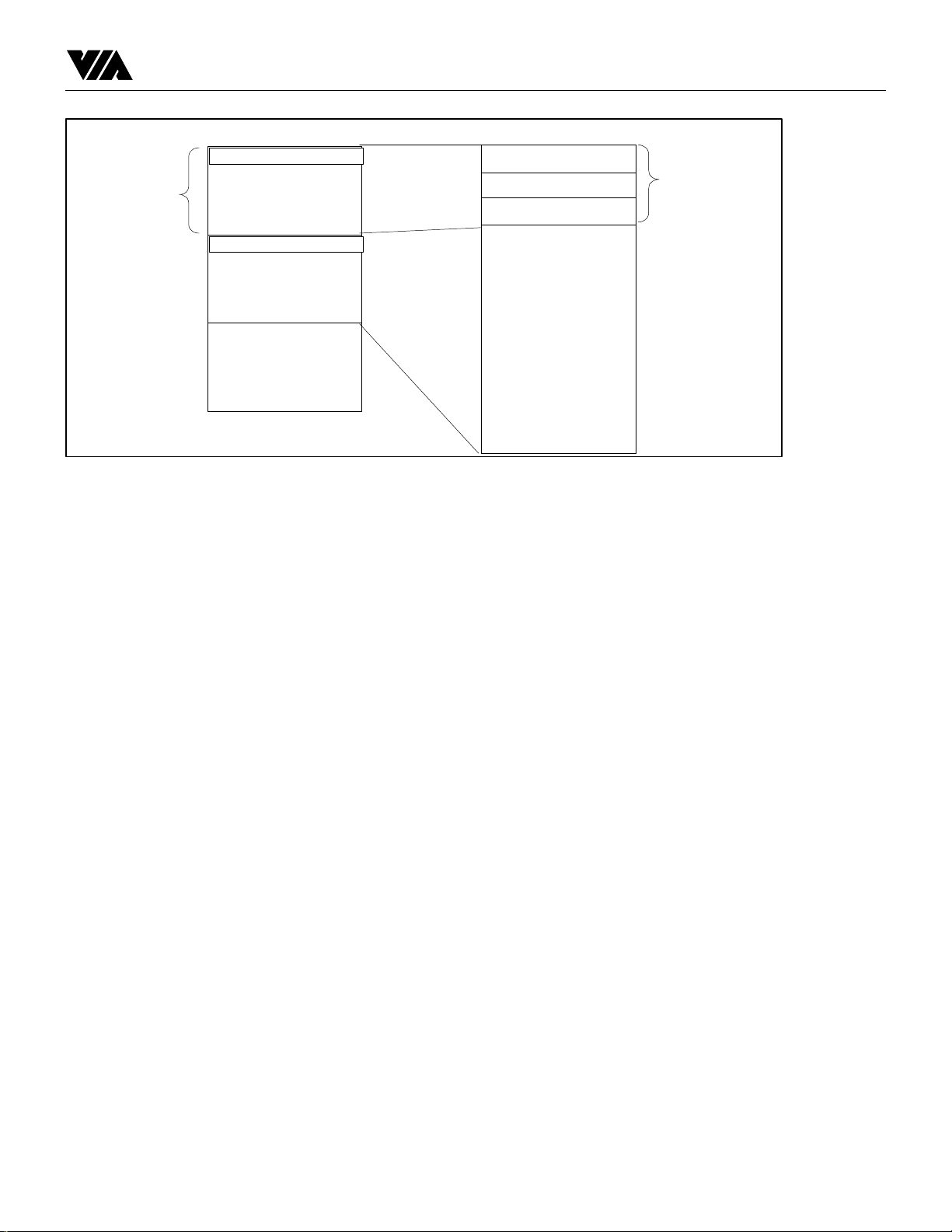
free permanent packet memory for that port. See Figure 3-4.
-20-
Page 21
VIA Technologies, Inc. Preliminary VT6516 Datarsheet
128 entries
SRAM
12 bytes/entry
Permanent Buffer
Table
12 bytes/entry
Free List
Link Table
Address Table
Entriers
DRAM
1.5 K/Packet
...
1.5 K/Packet
128 blocks
-21-
Page 22
VIA Technologies, Inc. Preliminary VT6516 Datarsheet
List 0
List 1
Link/
Frame
128/0
129/0
130/1
131/0
132/1
133/1
134/0
135/1
136/0
16MBits SDRAM
Memory Bank
2K
2K
2K
2K
2K
2K
2K
Bank 0
Bank 1
List 0
List 1
Links/
List
128/0
129/0
130/0
131/1
132/1
133/1
134/0
135/0
136/1
137/1
Memory Bank
4K
4K
4K
4K
64MBits SDRAM
Bank 0
Bank 1
Figure 3-3
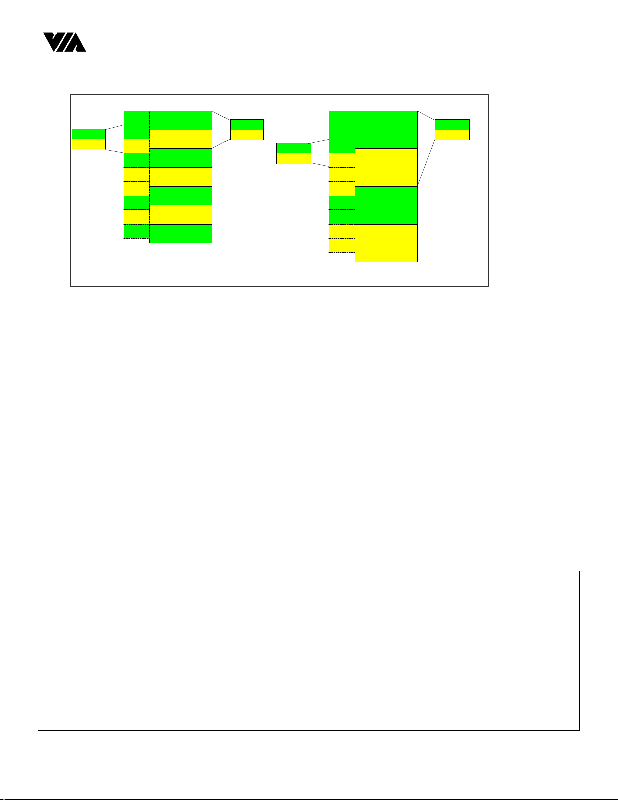
Following as the listing and figure 3-6 is the algorithm of initialization procedures for 2 bank free list of
SDRAM.
For 16 Mbit SDRAM as following,
-- Bank0 free link list:
128, 129, 131, 134, 136, 137, 139, 142, 144, 145, 147, 150, 152, 153, 155, 158, 160,...
-- Bank1 free link list:
130, 132, 133, 135, 138, 140, 141, 143, 146, 148, 149, 151, 154, 156, 157, 159, 162, 164, ...
For 64 Mbit SDRAM as following,
-- Bank0 free link list:
128 , 129 , 130 , 134 , 135 , 139 , 140 , 141 , 144 , 145 , 146 , 150 , 151 , 155 , 156 , 157 , 160 , ...
--Bank1 free link list:
131 , 132 , 133 , 136 , 137 , 138 , 142 , 143 , 147 , 148 , 149 , 152 , 153 , 154 , 158 , 159 , 163 , …
Figure 3-6: Algorithm of Initialization of Free Link Lists.
#define SRAM_ADDR_REG0 0x2001
#define SRAM_ADDR_REG1 0x2002
#define SRAM_ADDR_REG2 0x2003
#define SRAM_DATA_REG0 0x2004
#define SRAM_DATA_REG1 0x2005
#define SRAM_DATA_REG2 0x2006
#define SRAM_DATA_REG3 0x2007
#define SRAM_CMD_REG 0x2008
#define SRAM_STATUS_REG 0x2009
#define SRAM_ACCESS_IDLE 0x01
#define NULL_PTR 0x7FFFF
void writeLinkEntry(int entryID, int nextID)
{
reg_byte_write (SRAM_ADDR_REG0, entryID*3 & 0x0FF);
reg_byte_cont_write (((entryID*3) >> 8) & 0x0FF);
reg_byte_cont_write (((entryID*3) >> 16) & 0x0FF);
-22-
Page 23

VIA Technologies, Inc. Preliminary VT6516 Datarsheet
reg_byte_cont_write (nextID & 0x0FF); // data bits [7:0]
reg_byte_cont_write ((nextID >> 8) & 0x0FF); // data bits [15:8]
reg_byte_cont_write ((nextID >> 16) & 0x0FF); // data bits [23:16]
reg_byte_cont_write (0); // data bits [31:24]
reg_byte_cont_write (0x02); // SRAM-write command
while (reg_byte_read(SRAM_STATUS_REG) != SRAM_ACCESS_IDLE) {}
}
void initFreeList16Mb(int maxLinkEntryNo)
{ // note: for 16Mb SDRAM,
// Bank0 free list head pointer = 128
// Bank1 free list head pointer = 130
int k; // k: current free entry id
int b0, b1; // b0, b1: bank0/1 free list head entry id
for(b0=b1= NULL_PTR, k= maxLinkEntryNo; k <=128; k--)
if (((k * 3) % 8) < 4)
{ writeLinkEntry(b0,k); b0=k;}
else { writeLinkEntry(b1,k); b1=k;}
}
void initFreeList64Mb(int maxLinkEntryNo)
{ // note: for 64Mb SDRAM,
// Bank0 free list head pointer = 128
// Bank1 free list head pointer = 131
int k; // k: current free entry id
int b0, b1; // b0, b1: bank0/1 free list head entry id
for(b0=b1= NULL_PTR, k= maxLinkEntryNo; k <=128; k--)
if (((k * 3) % 16) < 8)
{ writeLinkEntry(b0,k); b0=k;}
else { writeLinkEntry(b1,k); b1=k;}
}
-23-
Page 24
VIA Technologies, Inc. Preliminary VT6516 Datarsheet
3.1.1 SDRAM interface
All frames received by the VT6516 will be stored into a common frame buffer memory, SDRAM.The
SDRAM contains the packet buffers, each buffer is a 1536 (1.5K) bytes memory block. Each block is
associated to an entry in link table in SRAM. The link entry includes a field (19 bits to support 512 MB) to
point to next link entry. The figure 3-2 is buffer link list structure.
In order to provide the cost effective DRAM buffers, user can connect the 32 bits data SGRAM with
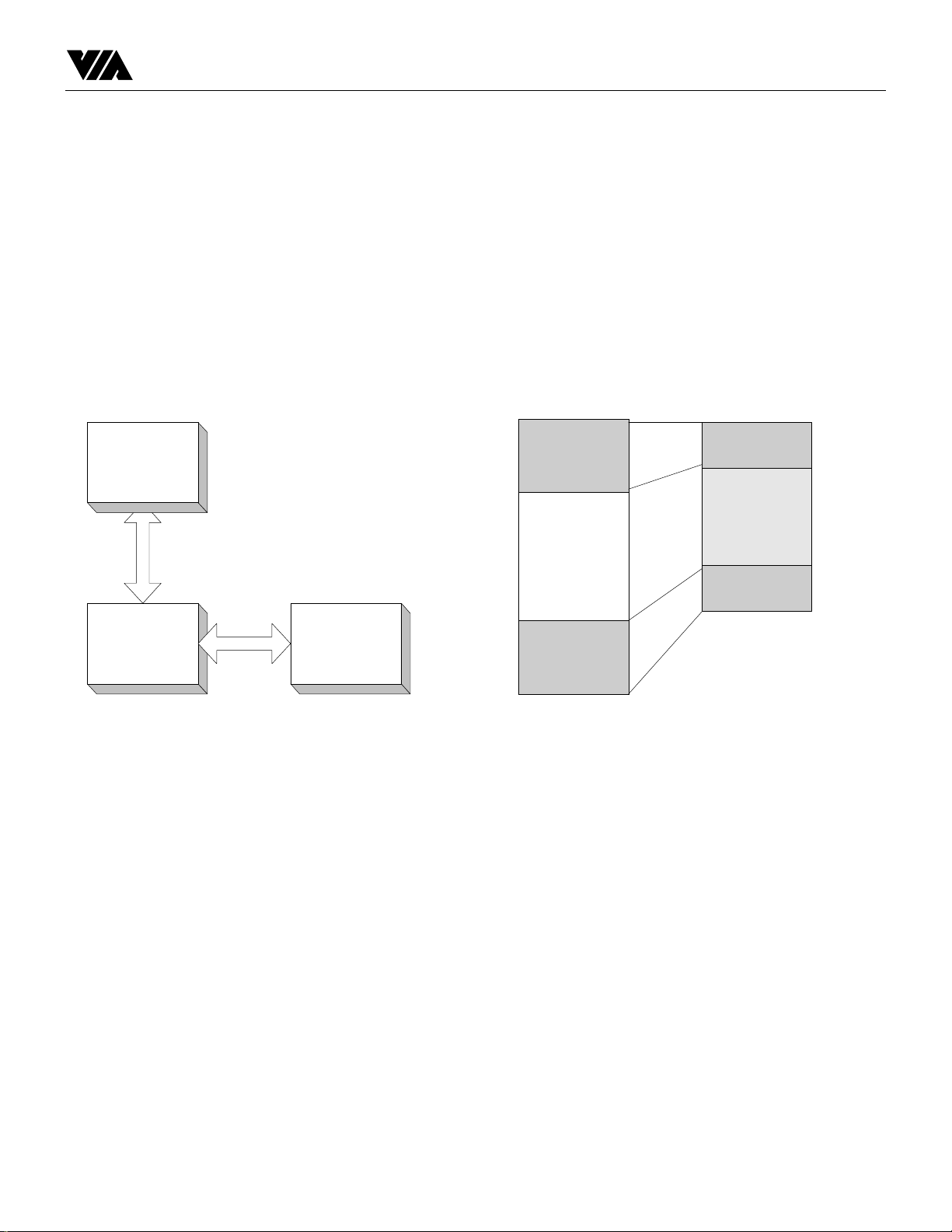
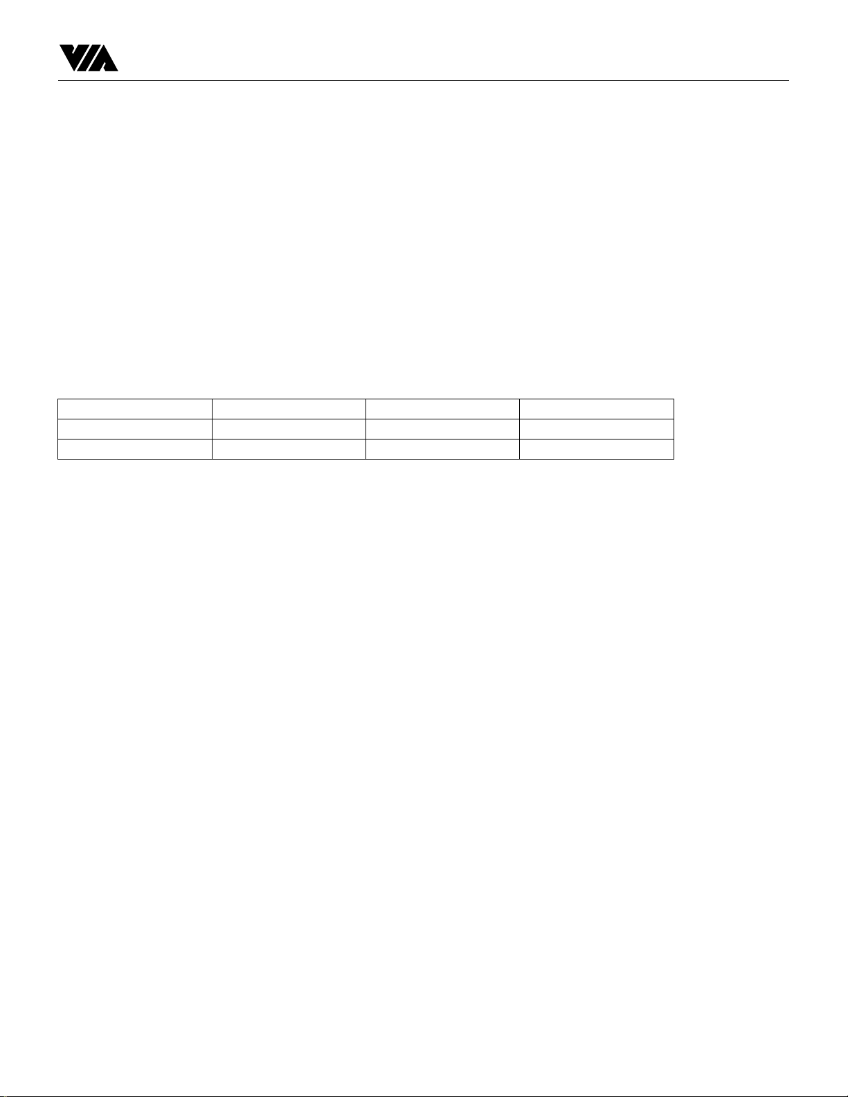
VT6516 switch, there are two external buffer device using two double bank 128Kbits by 32 required. The
following figure shows the minimum configuration of buffer memory and link/address memory. Note that the
SGRAM physical memory hole is to accommodate the forwarding table into the SRAM link list hole.
32*32 (128Kb)
SSRAM by one
VT6516
128K*32*2
(2MB)
SGRAM by two
Physical Device
(1MB)
Memory Hole
(14MB)
Physical Device
(1MB)
Physical Buffer Memory
Allocation (eg, 2MB)
Link List
Address table
entries
(Link-List Hole)
Link List
Physical SRAM Memory
Allocation (eg, 128K)
-24-
Page 25
VIA Technologies, Inc. Preliminary VT6516 Datarsheet
The detail initial step of VT6516 as following,
1. Forwarding table base = 683 * 3
2. SDRAM type equal to 16M bit
3. END0-3 = 2 (16MB)
4. Free list of SRAM have to be constructed by release public node in the sequence of buffers with blocks
number
10922, 10911, …. 10240, 681, 680, 128
Note: The buffers numbered 682 to 10239 are located in the buffer memory hole, those buffers will be not
put into the free list.
5. Free Memory count equal to 1364
Otherwise like this minimum configuration, the entries support for difference SRAM size using normal
Address table followed by free-list, the following table show the address entries support
Buffers 32*32 SSRAM 64*32 64*64
2MB 8K entries 8K~16K 8K~64K
4MB 8K entries 8K~16K 8K~64K
-25-
Page 26
VIA Technologies, Inc. Preliminary VT6516 Datarsheet
3.1.2 SRAM interface
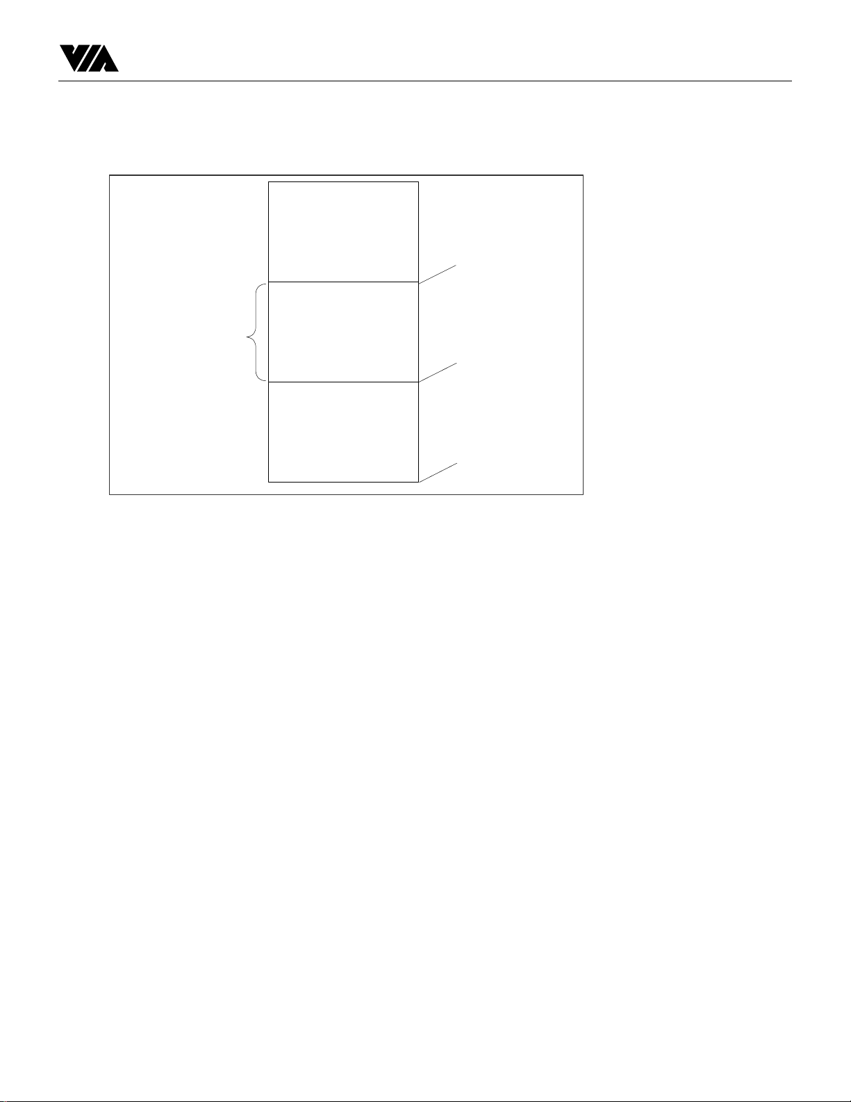
The feature 3-1 is SSRAM structure map, the SSRAM contains the forwarding address entries, SDRAM
buffers link list and permanent buffers table.
Link table Entries * 12
bytes/entry
(FREECNT(1006H) * 1.5K)
High
Low
Permanent Link
Table
Link Table
Address Table
Entries
Figure 3-1 SRAM
0
16 ports * 8 * 12
bytes/entry
Forwarding Table
start address
(TABLE_BASE(1401H)
)
Address Entries * 12
bytes/entry
HASH_BITS(1400H)
(2
* 12)
-26-
Page 27
VIA Technologies, Inc. Preliminary VT6516 Datarsheet
54
reserved
6595
64 59
VLAN ID
58
VLAN
tage flag
57 55
frame
tag type
priority
52 51
frame
type
Figure 3-2 Free buffer link structure
Table 1-0 Free buffer link structure
bit 18-0 Next entry pointer
bit 35-19 port mask (bit[16]: CPU port + bit[15:0]: Ethernet ports 0~15)
bit 46-36 Packet byte count
bit 50-47 Source port ID
bit 51 Frame type Reserved (zero)
Bit 54-52 Priority
Bit 57-55 Frame tag type Reserved (zero)
bit 58 VLAN tag flag Reserved (zero)
bit 64-59 VLAN ID
bit 95-65 reserved for future
47
50
source
port ID
46
packet byte
count
36
35 19
port
mask
16 ports
+1 cpu
18
pointer to
next entry
0
95
reserved
64
VLAN ID
57
VLAN
tage flag
56
static/dynamic
flag
55
count
age
54
53 3736
port
mask
16 ports
+1 cpu
bit-47:11
MAC address
fixed, even for key
length = 11~15
063 58
Figure 3-5 The Address table entries structure +
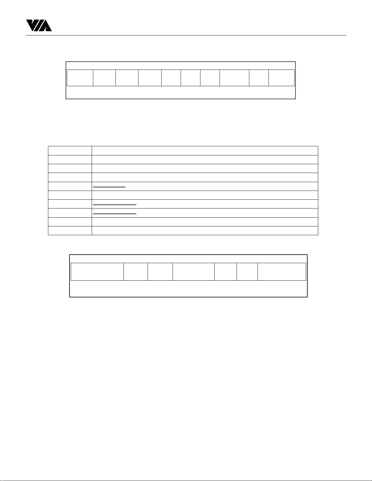
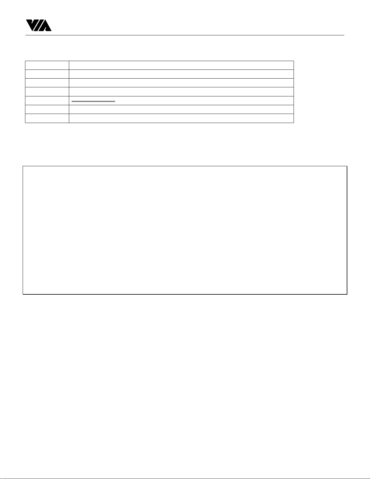
The address table structure as figure 3-5, The address table entries contains the MAC address information
from bit 11 to bit 47, others bits 0~10 or bits 0~14 (2K~32K) as the address entries hashing index, the total
address entries of device assigned by the HASH_BITS(1400H).
Initialization procedures include to set forwarding address table control in normal mode and to invalidate all
forwarding table entries by setting the age-count field as 0. Configure port mask register (USER_PM) for
broadcast MAC address. Configure port mask and MAC address pairs that allow any static MAC to port
mask mapping.
Forwarding table entry has 96 bits, defined as follows:
-27-
Page 28
VIA Technologies, Inc. Preliminary VT6516 Datarsheet
Table 1-1 Address table structure
bit 36-0 High bits (bit 47-11) of MAC address
bit 53-37 port mask (bit[16]: CPU port + bit[15:0]: Ethernet ports 0~15)
bit 55-54 age count
bit 56 Static flag (0: dynamic entry, 1: static entry that can not be updated)
bit 57 VLAN tag flag Reserved (zero)
bit 63-58 VLAN ID
bit 95-64 Reserved for future
And following is the algorithm for the initial the address entries;
#define SRAM_ADDR_REG0 0x2001
#define SRAM_ADDR_REG1 0x2002
#define SRAM_ADDR_REG2 0x2003
#define SRAM_DATA_REG0 0x2004
#define SRAM_DATA_REG1 0x2005
#define SRAM_DATA_REG2 0x2006
#define SRAM_DATA_REG3 0x2007
#define SRAM_CMD_REG 0x2008
#define SRAM_STATUS_REG 0x2009
#define SRAM_ACCESS_IDLE 0x01
void invalidateForwardEntry(int entryID)
{ // the entryID is starting from maxLinkEntryID with width of 96 bits
reg_byte_write (SRAM_ADDR_REG0, (entryID*3+1) & 0x0FF);
reg_byte_cont_write (((entryID*3+1) >> 8) & 0x0FF);
reg_byte_cont_write (((entryID*3+1) >> 16) & 0x0FF);
reg_byte_cont_write (nextID & 0x0FF); entry bits [32]
reg_byte_cont_write ((nextID >> 8) & 0x0FF);
reg_byte_cont_write ((nextID >> 16) & 0x0FF);
reg_byte_cont_write ((nextID >> 16) & 0x0FF);
reg_byte_cont_write (0x02); // SRAM-write command
while (reg_byte_read(SRAM_STATUS_REG) != SRAM_ACCESS_IDLE) {}
}
3.1.3 CPU interface
The VT6516 support one ISA-like CPU interface, this CPU interface can cooperate with one simple
microprocessor like 8031 or 8051. The CPU will access the switch control and status register to perform
initialization and configurations. By the CPU interface, the frames of CPU port can be read/written from/into the
buffer. The CPU interface can also be used to access the internal registers. The CPU interface also used to access
the external PHY devices through the PHY control module.
The CPU firmware will perform following tasks,
- Read the configuration from switch register or from the EEPROM contains
- Initialize the switch followed by the configuration, those task including
* DRAM initialization
* SRAM initialization and link list construction
* Program for each network ports for users manual setting or read the auto-negotiation result
- start switch to receive frames and forward frames
- decrease the learning address aging count
- polling the network port change event and change the switch MAC negotiation mode.
-28-
Page 29

VIA Technologies, Inc. Preliminary VT6516 Datarsheet
- Receiving the STP defined BPDU packets
- Blocking or re-start port due to STP
- Access the network management counter of each port
For a management switch the CPU also perform the management function like receiving and transmitting
the SNMP frame.
-29-
Page 30
VIA Technologies, Inc. Preliminary VT6516 Datarsheet
3.1.4 Network interface
The VT6516 directly connect to 16 port RMII PHY or 12 port MII PHY device which compliant with
IEEE standard (Please see IEEE 802.3u Fast Ethernet standard) . Each Fast Ethernet port has following
characteristics:
- Capable of supporting both 10MBps and 100MBps data rates in half and full duplex modes.
- Provide a simple management interface (SMI) for port status
- Perform all functions of the IEEE 802.3 protocol such as frame formatting, frame stripping, collision
handling, deferred, etc.
- Adjustable preamble ,SFD and inter frame gap (IFG).
- IEEE 802.3X flow control supported
- IEEE 802.1D spanning tree protocol support, and all port state of listen and block configurable
3.1.4.1 RMII interface
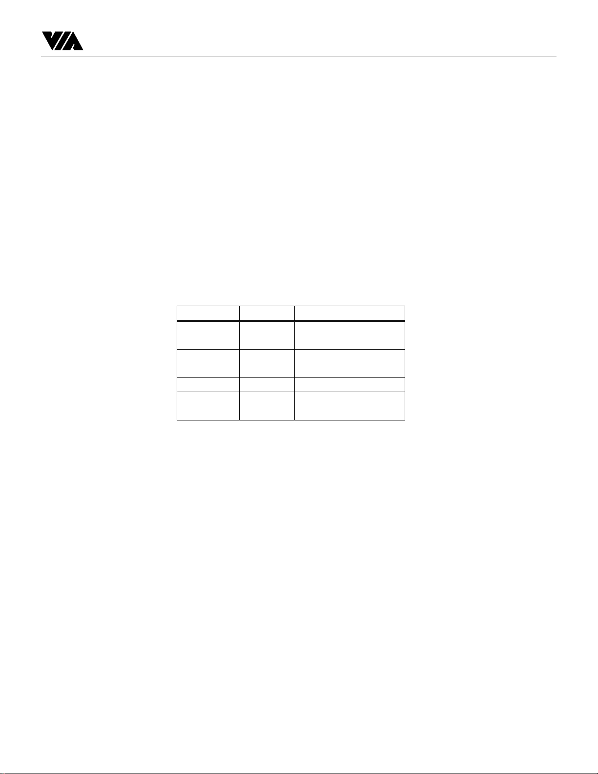
The VT6516 communicates with the external 10/100M Ethernet transceiver through the reduced MII
(RMII) interface. The signals of RMII interface are described in Table-3-1
Table 3-1 RMII interface signals
Name Type Description
CRSDV I Carrier sense and Data
valid
RXD[0-1] I Receive data bit 0 to 1 ,
data rate with 50MHz
TXEN O Transmit Enable
TXD[0-1] O Transmit Data bit 0 to
1
Figure 3-1 RMII timing diagram
(omitted)
-30-
Page 31
VIA Technologies, Inc. Preliminary VT6516 Datarsheet
3.1.4.2 MII interface
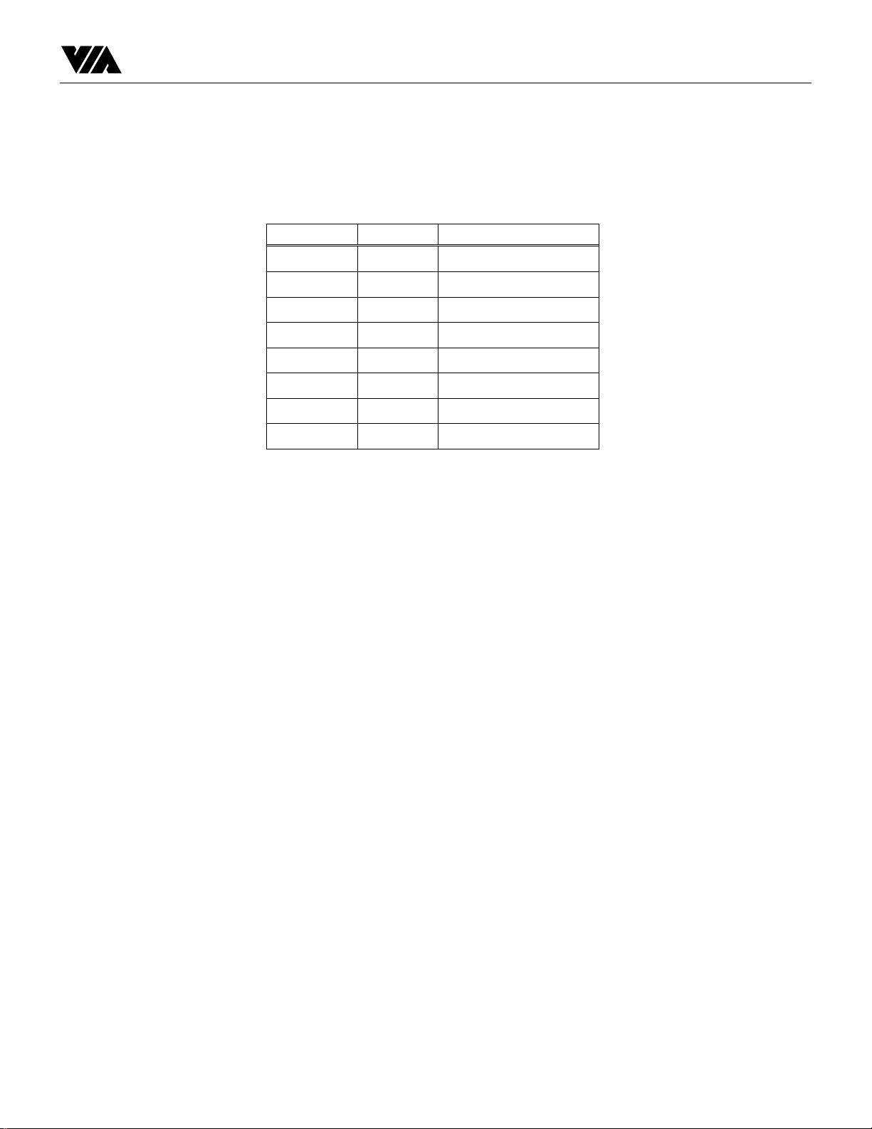
The VT6516 communicates with the external 10/100M Ethernet transceiver through standard MII
interface, in this mode the VT6516 became 12 ports MII port due to the MII signal multiplexed with RMII
signal. But the ports number of internal remained as 16 ports. The signals of MII interface are described in
Table-3-2:
Table 3-2 MII interface signals
Name Type Description
TCLK I
TXD[3:0] O
TXEN O
COL I
CRS I
RXD[3:0] I
RCLK I
RXDV I
Figure 3-2 MII timing diagram
3.1.4.3 Flow control
Under full-duplex mode operation, if the buffer utilization of whole switch has exceeded the upper threshold
and the permanent buffer has been used up, a pause frame with a pause time interval will be send to the sending
port to stop it from sending new frame. If register- FMFCT not enable at this switch, the public buffer will used
until no more buffers. Then further incoming frames will be dropped. The unit in pause time field of the flow
control frame is slot time (512 bits).
The max possible waiting time should be the max packet memory size divided by lowest port speed, for example
if 512MB is the max packet buffer size and 10Mb is the lowest speed, the 512M * 8 bits * 100ns = 409.6 seconds
(8M slot time) is the max possible waiting time. The congestion factor is the max possible waiting time at current
link load. The pause timer value is half of the max possible waiting time. If it is greater than the feasible max
pause time, use all 1’s in pause time value.
If the utilization of the public buffer of the switch drops below the lower threshold, a pause-frame with minimum
frame interval of 0 will be sent to the linking ports the enable new frame transmission.
Under half duplex operation, if the buffer utilization of whole switch has exceeded the upper threshold and the
permanent buffer has been used up, the port will perform back-pressure based flow control by sending a jam
pattern on each incoming frame. If backpressure flow control of the port is not enable, the frame will be dropped.
The flow control pause time is calculated by maintained the configuration of port speed of each port and the
buffer size. With input of the free memory block count and congestion factor, it determines flow control on or
off on an output port. If flow control is on, any new queue request from a input port to this output port will
trigger a flow control frame sent to that request port by the output MAC that is notified by the packet flow
control unit.
Transmit Clock
Transmit Data for.
Transmit
Collision Detected
Carrier Sense
Receive Data
Receive Clock
Receive Data
(omitted)
-31-
Page 32

VIA Technologies, Inc. Preliminary VT6516 Datarsheet
The flow control activity is triggered when the buffer utilization exceeds certain thresholds specified by the
dedicated register FMFCT, Register- FMFCT is used to specify the upper and lower thresholds of reserved
buffer slot for whole switch.
3.1.4.4 SMI interface
The VT6516 communicates with the external 10/100M PHY and access the PHY register through MDC, MDIO
3.1.4.5 Auto negotiation
The VT6516 communicates with the external 10/100M PHY and access the PHY register through MDC, MDIO
3.1.5 Serial EEPROM interface
-32-
Page 33

VIA Technologies, Inc. Preliminary VT6516 Datarsheet
4. FUNCTIONAL DESCRIPTION
4.1 Packet Reception and Address recognition
When VT6516 received frames from network, the input control module will receive packet from input MAC
module, then get the output port mask from forwarding table control module, request packet buffer from buffer
control, write packet from input FIFO to packet buffer scheduled by scheduler module, queue packet to the
output queue through queue control module. And update the forwarding table by the source address of the
received good packet.
Usually the source MAC address will be learned and stored to forwarding table. If VLAN is configured by user,
the frame tag type and VLAN ID will also be learned. The source MAC address bit 47~11 and VLAN ID will be
record in the forwarding table entry indexed by source MAC address bit 10~0 or 14~0.
The on chip multicast forwarding configuration registers mainly are for well-known addresses which are listened
by CPU. External multicast addresses are for dynamically assigned. Also some static Mac addresses/port mask
registers can be configured by CPU, these addresses will also be checked before look up the forward table.
4.2 Packet Forwarding and VLAN
The VT6516’s queue control maintains all head and tail pointers for all output ports. Accept the request to
queue and dequeue packets from input and output control.
Both queue and dequeue operations take only 1 SRAM access (3 words = 96 bits), because the tail node is
stored in the internal register of the queue control
Usually, queue and dequeue operations to a specific output queue can be performed simultaneously. However,
mutual exclusion is applied while only one node in this queue
Each port will maintain a packet counter, it increments when packet gets queued through the tail pointer, it
decrements when packet de-queued through head pointer. The congestion factor is the queued packet count
divided by port media speed. The congestion factor will be used for flow control and multicast, congestion
factor should be roughly equal to the time it takes to transmit all the queued packets.
For multicast packet, based on congestion factor, the least congested output port will be queued first. The
output control will queue the packet to next least congested output port when it is transmitted, the CPU port will
always be last port to be transmitted if the corresponding CPU bit is set in the port mask.
The port speed will be used for cut through forwarding decision. If the packet length is 7ff, it implies the input
control try to cut through, queue control will accept or reject by looking whether the input port speed is equal to
the output port speed and the output don’t have queued packets and any pending transmission. The faster
output port (than input port speed) and CPU port is not able to cut through
Broadcast packet, multicast and look up miss packet will forward(multicast) to those ports which is configured
by software, but default(dump switching hub) will be all ports(or all ports in that VLAN if VLAN is
implemented) except CPU port. Broadcast, multicast packet will check the on chip broadcast forwarding
configuration register and multicast forwarding configuration registers first, if multicast address not match any
of the multicast forwarding configuration registers then it will look up the external SRAM forwarding table.
-33-
Page 34

VIA Technologies, Inc. Preliminary VT6516 Datarsheet
When request transfer to or from SDRAM through scheduler, the input control need to derive each burst
starting address to bank0 or bank1 information for scheduler to utilize SDRAM bandwidth efficiently. When
input FIFO is filled to 12x64 or page boundary or end of frame, the input port control will request DRAM access
to write packet. Input FIFO size is 64 bits by 24.
After receiving the grant of queueing (cut-through or store-and-forward), even the bad packet has to be
forwarded.
While cut-through, the input control will request the grant of cut-through counter bus for passing the cut
through packet count from input port to output port as the whole packet has received.
4.2.1 Cross VLAN Server Port support
The VT6516 support Cross VLAN server port configuration, the following illation show the sample of
server ports configuration by set the register of server port mask(14A0H~14A1H), and server ports only enable
after the VLAN enabled. The multicast or broadcast frames received from one VLAN group will forward to any
server ports and only forward to the ports with same VID.
4.3 Network Management Features
Flow control
The flow control activity is triggered when the buffer utilization exceeds certain thresholds specified by
the dedicated register XXXX, Register-XXXX is used to specify the upper and lower thresholds of reserved
buffer slot for whole switch.
Under full-duplex mode operation, if the buffer utilization of whole switch has exceeded the upper
threshold and the permanent buffer has been used up, a flow control with a predefined pause time value will
be sent to the source port to stop the input traffic. If flow control mechanism is not enabled, the public buffer
will exhausted so that the further incoming frames will be dropped.
Under half duplex operation, if the buffer utilization of whole switch has exceeded the upper threshold
and the permanent buffer has been used up, the port will perform back-pressure based flow control by
sending a jam pattern on each incoming frame. If backpressure flow control of the port is not enable, the
frame will be dropped.
Sniffer port
The VT6516 support sniffer function for user to monitor the network traffic. The Sniffer port enable can
be set for any individual port of sixteen ports. And each sniffer port can set to monitor the traffic coming
from any others fifteen port(monitor port). Any packets sent to the monitor ports or transmitted out of
monitor port will be forwarded to sniffer port.
Spanning tree support
The VT6516 support the spanning tree protocol (STP). When spanning tree protocol support is enabled,
frames from the CPU port having a DA value equal to reserved Bridge Management Group Address for
BPDU will be forwarded to the port specified by the CPU. Frames from other port with a DA equal to
reserved Bridge Management Group Address for BPDU will be forwarded to the CPU port.
-34-
Page 35

VIA Technologies, Inc. Preliminary VT6516 Datarsheet
Every port of the VT6516 can be set to block and listen mode through the CPU interface. In the mode,
incoming frames with DA value equal to the reserved Group address for BPDU will be forward to CPU port
and other incoming frames with other DA value will be dropped. Outgoing frames with any DA value will be
filtered expect DA equal to BPDU.
-35-
Page 36
VIA Technologies, Inc. Preliminary VT6516 Datarsheet
SECTION II REGISTER MAP
1. REGISTER TABLES
The VT6516 incorporates the required command/status registers and various counters for management
purposes. Although the default values of the control registers are predefined in the usual way, there is still a
requirement for CPU intervention. All registers are defined as 8 bits so that long registers have to be divided into
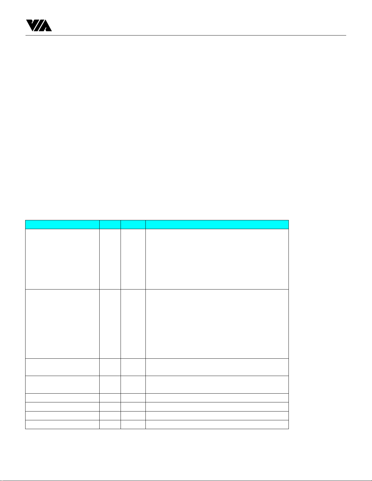
pieces of 8 bits with the Little-Endian principle, i.e. the lower byte in the lower address. There are only eight
registers that are directly accessible for CPU, called the CPU interface registers. They are located with memory
mapping in the range of 8000H ~ 8007H for the microprocessor 8031 in the evaluation board. The other
registers are called the internal registers that are referenced indirectly by the 16-bit address register with offset
02H ~ 03H in the CPU interface address table. While the 16-bit address register is set to reference to the specific
8-bit internal register, the following read or write operation to the 8-bit data register with offset 01H in the CPU
interface address table will cause the specified internal register to be read or written indirectly. Besides, the
address register will increase by one automatically to facilitate the successive read/write operation. If the internal
register is of size less than 8 bits, the value 0’s is always returned for the vacant register space and any write
operations to them take no effect.
2 CPU INTERFACE REGISTERS MAP
*Note: register table base = 8000H for the evaluation board.
Description Type Offset Function
Packet Data Register
[15:0]
Data Register [7:0] R/W 1H The read or write operation to the 8-bit data
Address Register [7:0] R/W 2H The low-byte address register for the reference to
Address Register [15:8] R/W 3H The high-byte address register for the reference
TEST Register 0 [7:0] W/O 4H see the description in TEST Register 3
TEST Register 1 [7:0] W/O 5H see the description in TEST Register 3
TEST Register 2 [7:0] W/O 6H see the description in TEST Register 3
TEST Register 3 [7:0] W/O 7H
R/W 0H According to the strapping mode of packet
read/write data bus, two types are defined for 8bit and 16-bit data bus, respectively. For 8-bit
CPU, only the low byte of the Packet Data
Register is used for packet read/write. For 16-bit
CPU, the whole 16-bit Packet Data Register is
used for packet read/write.
register will cause the specified internal register
(referenced by the Address Register) to be read
or written indirectly.
Besides, after the read/write operation, the
Address Register will increase by one
automatically to facilitate the successive
read/write operation.
an internal register with 16-bit address.
to an internal register.
-36-
Page 37
VIA Technologies, Inc. Preliminary VT6516 Datarsheet
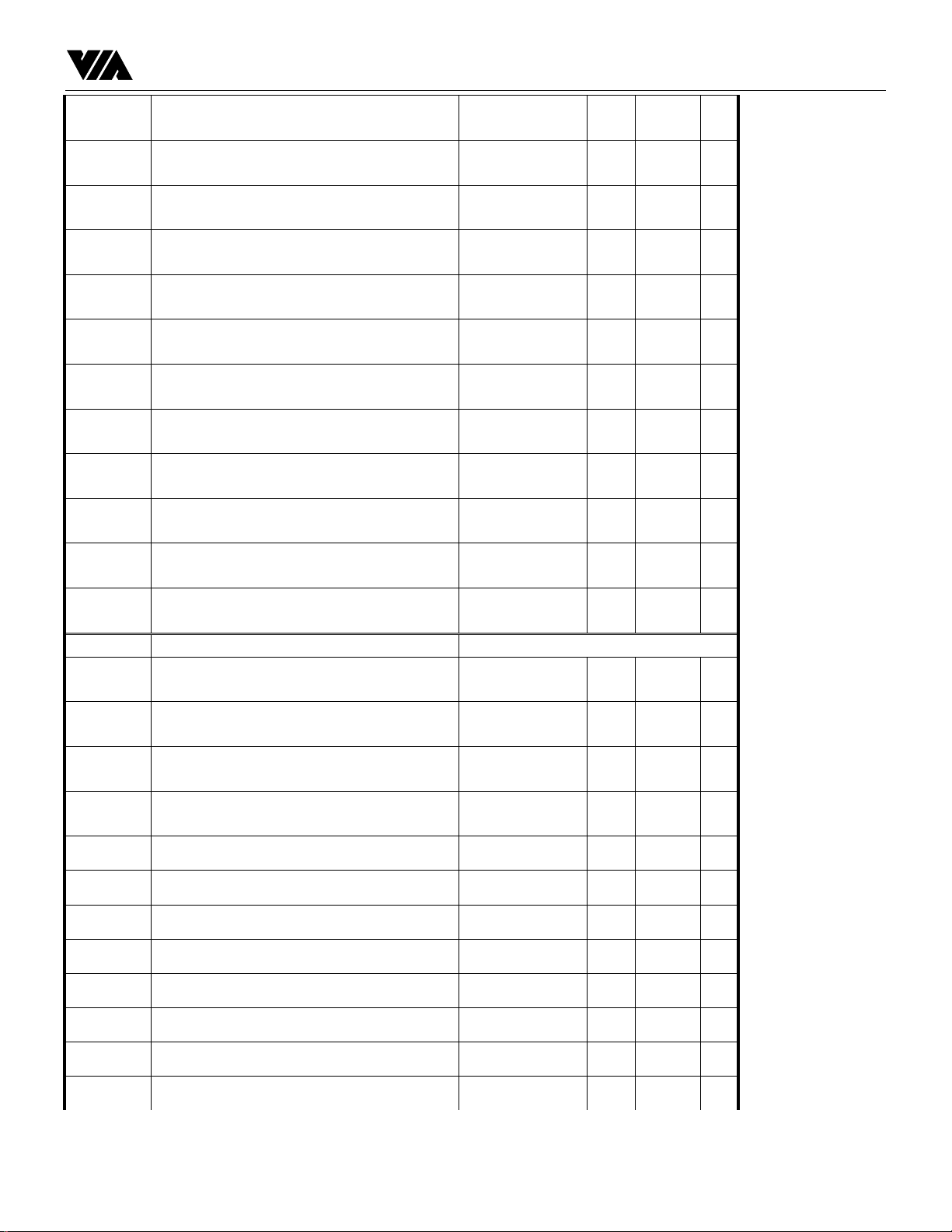
3 SWITCH INTERNAL REGISTERS MAP
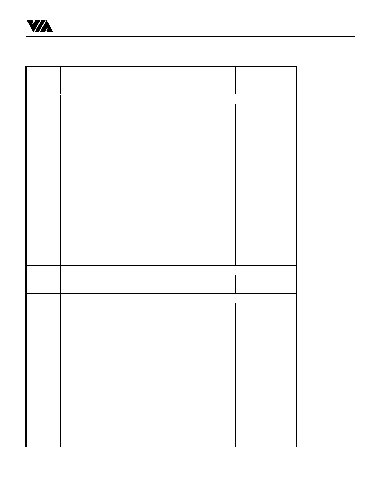
Address
(base/offse
Register Description Name Bits Default
ValueR/W
t)
0000H
00H
SDRAM
SDRAM TYPE SDRAMTYPE [0] 0 R/
W
01H CAS Latency CL [1:0] 2 R/
W
02H SDRAM Operation Mode RSDM [3:0] 5 R/
W
03H
DIM-Bank 0 Ending Address
END0A [4:0] 0 R/
W
04H DIM-Bank 1 Ending Address END1A [4:0] 0 R/
W
05H DIM-Bank 2 Ending Address END2A [4:0] 0 R/
W
06H
DIM-Bank 3 Ending Address
END3A [4:0] 0 R/
W
07H SDRAM Command Drive Strength
Configure
SDRAM_DR_CFG[2:0] 0 R/
W
08H SDRAM Bank Interleaving Disable BK_IL_DIS [0] 0 R/
W
0800H
00H
0C00H
00-02H
SRAM
SRAM Read Command Interleave Disable SRAM_READ_IL_D
IS
Queue control
Free Memory Flow Control Threshold register FMFCT
[0] 0 R/
W
[18:0]0 R/
W
03H Cut Through Enable CUT_THROU
GH_EN
04H
CPU Port Speed Configuration
CPU_SPD_CFG[2:0] 0 R/
[0] 0 R/
W
W
10-13H Congestion Factor of Output Port 0 CONGEST_FCT0[25:0]0
R/O
14-17H Congestion Factor of Output Port 1 CONGEST_FCT1[25:0]0 R/O
18-1BH Congestion Factor of Output Port 2 CONGEST_FCT2[25:0]0 R/O
1C-1FH Congestion Factor of Output Port 3 CONGEST_FCT3[25:0]0 R/O
20-23H Congestion Factor of Output Port 4 CONGEST_FCT4[25:0]0 R/O
-37-
Page 38
VIA Technologies, Inc. Preliminary VT6516 Datarsheet
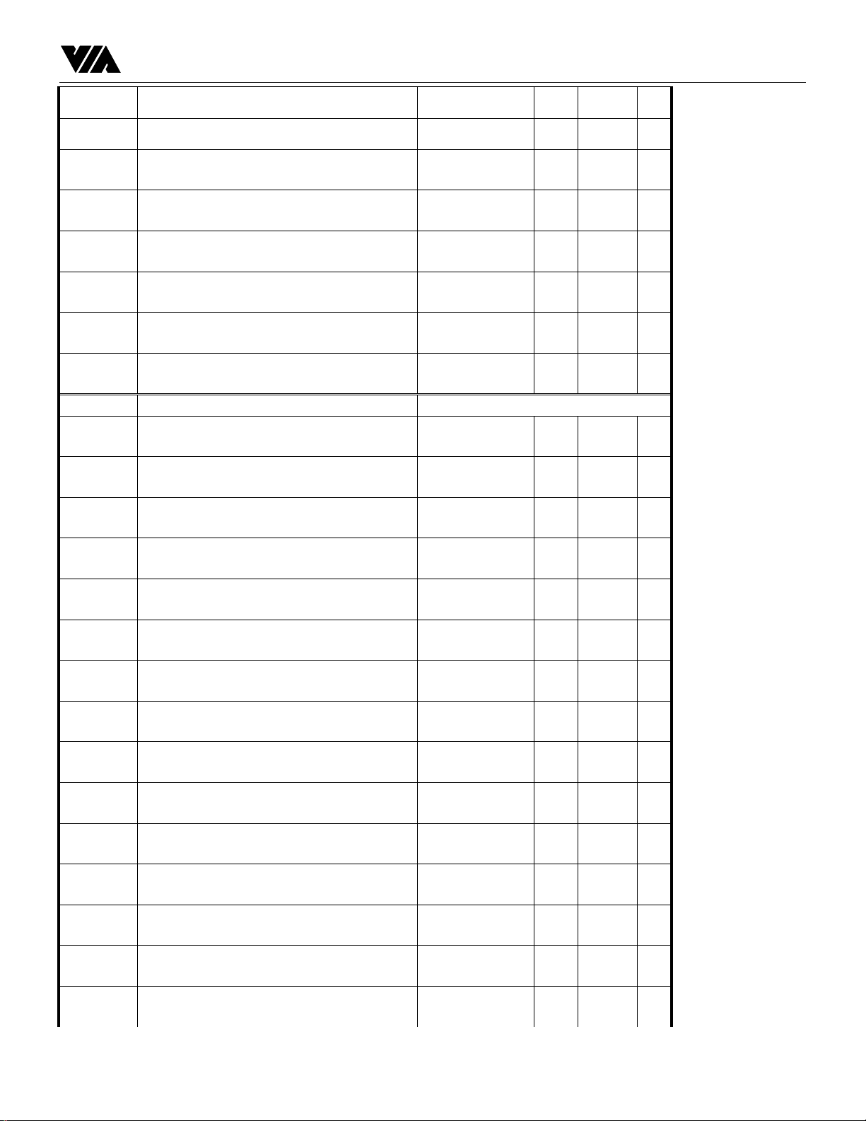
24-27H Congestion Factor of Output Port 5 CONGEST_FCT5[25:0]0 R/O
28-2BH Congestion Factor of Output Port 6 CONGEST_FCT6[25:0]0 R/O
2C-2FH Congestion Factor of Output Port 7 CONGEST_FCT7[25:0]0 R/O
30-33H Congestion Factor of Output Port 8 CONGEST_FCT8[25:0]0 R/O
34-37H Congestion Factor of Output Port 9 CONGEST_FCT9[25:0]0 R/O
38-3BH Congestion Factor of Output Port 10 CONGEST_FC
T10
3C-3FH Congestion Factor of Output Port 11 CONGEST_FC
T11
40-43H Congestion Factor of Output Port 12 CONGEST_FC
T12
44-47H Congestion Factor of Output Port 13 CONGEST_FC
T13
48-4BH Congestion Factor of Output Port 14 CONGEST_FC
T14
4C-4FH Congestion Factor of Output Port 15 CONGEST_FC
T15
50-53H Congestion Factor of Output Port 16
(CPU port)
CONGEST_FC
T16
1000H Buffer control
00-02H Bank 0 Free Pointer
03-05H Bank 1 Free Pointer
06-08H
09H CLEAR All Free Pointers (reset the free buffer
10H
11H
12H
13H
14H
15H
16H
17H
Free Memory Block Count
pointers according to the SDRAM TYPE)
PRIVATE MEMORY ALLOCATION BIT MASK for
PORT 0
PRIVATE MEMORY ALLOCATION BIT MASK for
PORT 1
PRIVATE MEMORY ALLOCATION BIT MASK for
PORT 2
PRIVATE MEMORY ALLOCATION BIT MASK for
PORT 3
PRIVATE MEMORY ALLOCATION BIT MASK for
PORT 4
PRIVATE MEMORY ALLOCATION BIT MASK for
PORT 5
PRIVATE MEMORY ALLOCATION BIT MASK for
PORT 6
PRIVATE MEMORY ALLOCATION BIT MASK for
PORT 7
FREE0_PT [18:0
FREE1_PT [18:0
FREEMCNT [18:0
CFP [0] W/
PORT0_MASK [7:0] 0 R/O
PORT1_MASK [7:0] 0 R/O
PORT2_MASK [7:0] 0 R/O
PORT3_MASK [7:0] 0 R/O
PORT4_MASK [7:0] 0 R/O
PORT5_MASK [7:0] 0 R/O
PORT6_MASK [7:0] 0 R/O
PORT7_MASK [7:0] 0 R/O
[25:0]0 R/O
[25:0]0 R/O
[25:0]0 R/O
[25:0]0 R/O
[25:0]0 R/O
[25:0]0 R/O
[25:0]0 R/O
R/O
]
R/O
]
R/
]
W
O
-38-
Page 39
VIA Technologies, Inc. Preliminary VT6516 Datarsheet
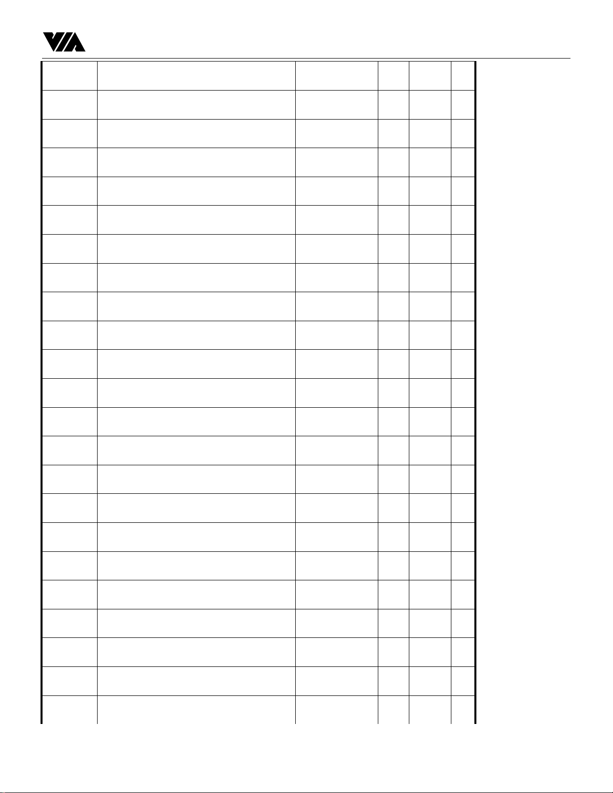
18H
19H
1AH
1BH
1CH
1DH
1EH
1FH
PRIVATE MEMORY ALLOCATION BIT MASK for
PORT 8
PRIVATE MEMORY ALLOCATION BIT MASK for
PORT 9
PRIVATE MEMORY ALLOCATION BIT MASK for
PORT 10
PRIVATE MEMORY ALLOCATION BIT MASK for
PORT 11
PRIVATE MEMORY ALLOCATION BIT MASK for
PORT 12
PRIVATE MEMORY ALLOCATION BIT MASK for
PORT 13
PRIVATE MEMORY ALLOCATION BIT MASK for
PORT 14
PRIVATE MEMORY ALLOCATION BIT MASK for
PORT 15
PORT8_MASK [7:0] 0 R/O
PORT9_MASK [7:0] 0 R/O
PORT10_MASK[7:0] 0 R/O
PORT11_MASK[7:0] 0 R/O
PORT12_MASK[7:0] 0 R/O
PORT13_MASK[7:0] 0 R/O
PORT14_MASK[7:0] 0 R/O
PORT15_MASK[7:0] 0 R/O
1400H Forwarding table control
00H bits of MAC address used as index for forwarding
table
01-03H
04H
starting SRAM address register for forwarding table
base
user configured forwarding mode
HASH_BITS [2:0] 0 R/
W
TBL_BASE [18:0]0 R/
W
FWD_MODE [1:0] 0 R/
W
05-07H
user configured port mask
USER_PM [16:0]0 R/
W
08-09H
port mask for packets sent by CPU
CPU_PM [15:0]0 R/
W
0AH CPU port related forwarding
configuration.
CPU_FWD_CFG[2:0] 0 R/
W
0BH port id of sniffer port. SNIFFER_PID [3:0] 0 R/
W
0C-0EH
monitor port mask MONITOR_PM [16:0]0 R/
W
10H high byte [14:8] of the MAC hash
address to be aged
11H low byte [7:0] of the MAC hash address
to be aged.
AGE_MAC [6:0] 0 R/
W
AGE_MAC [7:0] 0 R/
W
12H aging status AGING_STATUS[0] 0 R/O
20H spanning tree state for PORT 0 PORT0_STP_S
TATE
21H spanning tree state for PORT 1 PORT1_STP_S
TATE
22H spanning tree state for PORT 2 PORT2_STP_S
TATE
23H spanning tree state for PORT 3 PORT3_STP_S
TATE
-39-
[1:0] 0 R/
W
[1:0] 0 R/
W
[1:0] 0 R/
W
[1:0] 0 R/
W
Page 40
VIA Technologies, Inc. Preliminary VT6516 Datarsheet
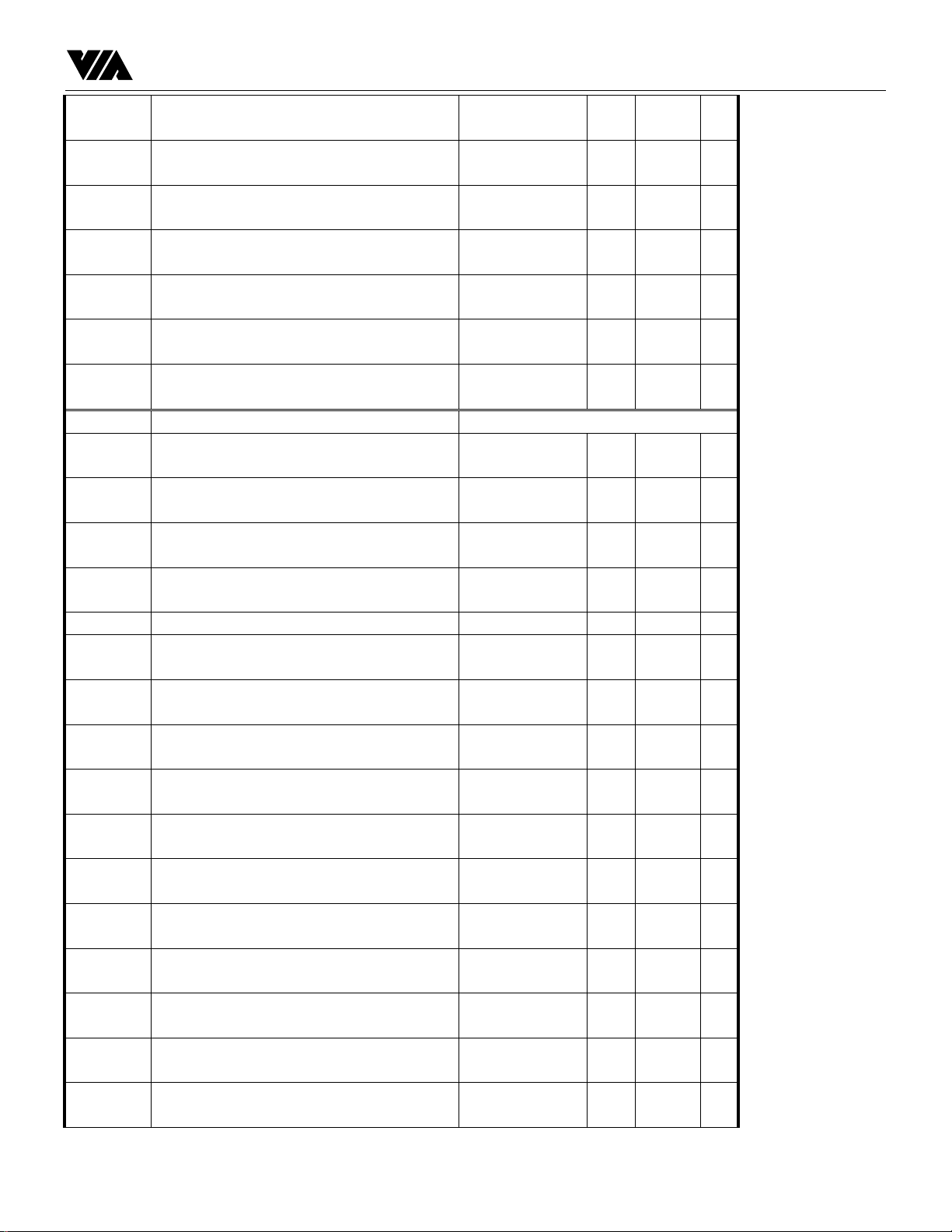
24H spanning tree state for PORT 4 PORT4_STP_S
TATE
25H spanning tree state for PORT 5 PORT5_STP_S
TATE
26H spanning tree state for PORT 6 PORT6_STP_S
TATE
27H spanning tree state for PORT 7 PORT7_STP_S
TATE
28H spanning tree state for PORT 8 PORT8_STP_S
TATE
29H spanning tree state for PORT 9 PORT9_STP_S
TATE
2AH spanning tree state for PORT 10 PORT10_STP_
STATE
2BH spanning tree state for PORT 11 PORT11_STP_
STATE
2CH spanning tree state for PORT 12 PORT12_STP_
STATE
2DH spanning tree state for PORT 13 PORT13_STP_
STATE
2EH spanning tree state for PORT 14 PORT14_STP_
STATE
2FH spanning tree state for PORT 15 PORT15_STP_
STATE
80H port 0 VLAN ID PORT0_VID [5:0] 0 R/
82H port 1 VLAN ID PORT1_VID [5:0] 0 R/
84H port 2 VLAN ID PORT2_VID [5:0] 0 R/
86H port 3 VLAN ID PORT3_VID [5:0] 0 R/
88H port 4 VLAN ID PORT4_VID [5:0] 0 R/
8AH port 5 VLAN ID PORT5_VID [5:0] 0 R/
8CH port 6 VLAN ID PORT6_VID [5:0] 0 R/
8EH port 7 VLAN ID PORT7_VID [5:0] 0 R/
90H port 8 VLAN ID PORT8_VID [5:0] 0 R/
92H port 9 VLAN ID PORT9_VID [5:0] 0 R/
94H port 10 VLAN ID PORT10_VID [5:0] 0 R/
[1:0] 0 R/
W
[1:0] 0 R/
W
[1:0] 0 R/
W
[1:0] 0 R/
W
[1:0] 0 R/
W
[1:0] 0 R/
W
[1:0] 0 R/
W
[1:0] 0 R/
W
[1:0] 0 R/
W
[1:0] 0 R/
W
[1:0] 0 R/
W
[1:0] 0 R/
W
W
W
W
W
W
W
W
W
W
W
W
-40-
Page 41
VIA Technologies, Inc. Preliminary VT6516 Datarsheet
96H port 11 VLAN ID PORT11_VID [5:0] 0 R/
W
98H port 12 VLAN ID PORT12_VID [5:0] 0 R/
W
9AH port 13 VLAN ID PORT13_VID [5:0] 0 R/
W
9CH port 14 VLAN ID PORT14_VID [5:0] 0 R/
W
9EH port 15 VLAN ID PORT15_VID [5:0] 0 R/
W
A0-A1H Server port mask SRV_PM [15:0]0 R/
W
A2H VLAN related forwarding configuration VLAN_FWD_CFG[0] 0 R/
W
1800H PHY control
00H PHY ID PHYID [3:0] 0 W/
O
01H PHY register address PHY_REG_ADDR[4:0] 0 W/
O
02-03H PHY data register PHYDATA [15:0
]
04H PHY command register PHYCMD [0] W/
05H PHY status register PHYSTS [1:0] 0 R/O
10H PORT0 PHY Device Address PORT0_PHY_
ADDR
11H PORT1 PHY Device Address PORT1_PHY_
ADDR
12H PORT2 PHY Device Address PORT2_PHY_
ADDR
13H PORT3 PHY Device Address PORT3_PHY_
ADDR
14H PORT4 PHY Device Address PORT4_PHY_
ADDR
15H PORT5 PHY Device Address PORT5_PHY_
ADDR
16H PORT6 PHY Device Address PORT6_PHY_
ADDR
17H PORT7 PHY Device Address PORT7_PHY_
ADDR
18H PORT8 PHY Device Address PORT8_PHY_
ADDR
19H PORT9 PHY Device Address PORT9_PHY_
ADDR
1AH PORT10 PHY Device Address PORT10_PHY_
ADDR
[4:0] 0 R/
[4:0] 0 R/
[4:0] 0 R/
[4:0] 0 R/
[4:0] 0 R/
[4:0] 0 R/
[4:0] 0 R/
[4:0] 0 R/
[4:0] 0 R/
[4:0] 0 R/
[4:0] 0 R/
R/
W
O
W
W
W
W
W
W
W
W
W
W
W
-41-
Page 42
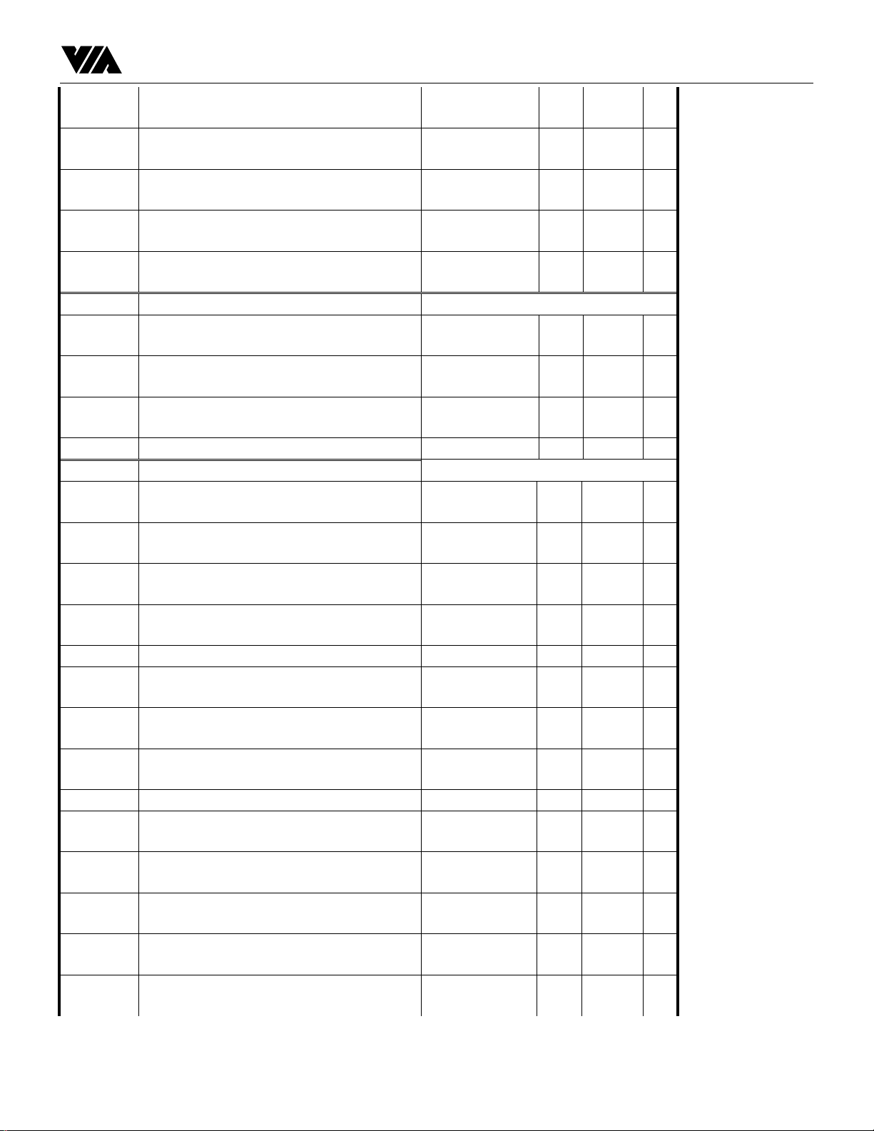
VIA Technologies, Inc. Preliminary VT6516 Datarsheet
1BH PORT11 PHY Device Address PORT11_PHY_
ADDR
1CH PORT12 PHY Device Address PORT12_PHY_
ADDR
1DH PORT13 PHY Device Address PORT13_PHY_
ADDR
1EH PORT14 PHY Device Address PORT14_PHY_
ADDR
1FH PORT15 PHY Device Address PORT15_PHY_
ADDR
1C00H EEPROM control
00H EEPROM word address EEWDADDR [7:0] W/
01H EEPROM data EEDATA [7:0] R/
02H EEPROM device address EEDEVADDR [7:0] W/
03H EEPROM status register EESTS [2:0] R/O
2000H CPU interface
00H interrupt status register IRQSTS [3:0] 0 R/
01H-03H SRAM address register SRAMADDR [18:0
04H-07H SRAM data register SRAMDATA [31:0
08H SRAM command register SRAMCMD [1:0] R/
09H SRAM status register SRAMSTS [1:0] 0 R/O
10H-13H SDRAM address register SDRAMADDR [23:0
14H-1BH SDRAM data register SDRAMDATA [63:0
1CH SDRAM command register SDRAMCMD [1:0] R/
1DH SDRAM status register SDRAMSTS [1:0] 0 R/O
20H Write packet command WR_PKT_CMD[2:0] W/
21H Packet Abort ERR_ABORT [0] W/
30H bits [47:40] of switch base MAC address
[47:0]
31H bits [39:32] of switch base MAC address
[47:0]
32H bits [31:24] of switch base MAC address
[47:0]
SWITCH_MA
C_BASE
SWITCH_MA
C_BASE
SWITCH_MA
C_BASE
[4:0] 0 R/
W
[4:0] 0 R/
W
[4:0] 0 R/
W
[4:0] 0 R/
W
[4:0] 0 R/
W
O
W
O
W
R/
]
]
]
]
[7:0] 0 R/
[7:0] 0 R/
[7:0] 0 R/
W
R/
W
W
R/
W
R/
W
W
O
O
W
W
W
-42-
Page 43
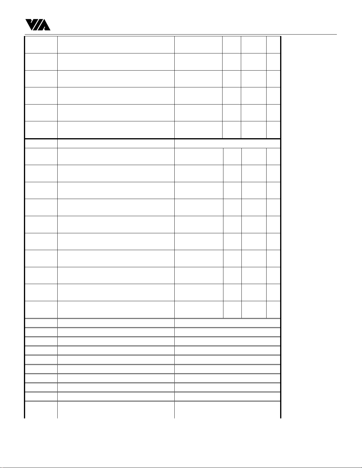
VIA Technologies, Inc. Preliminary VT6516 Datarsheet
33H bits [23:16] of switch base MAC address
[47:0]
34H bits [15:8] of switch base MAC address
[47:0]
35H bits [7:4] of switch base MAC address
[47:0]
40H interrupt mask register IRQSTS_MASK[3:0] 4’b1111 R/
50H CPU Soft Reset for the whole switch chip
reset
51H Revision Control Register REVISION_CTL[7:0] 0 R/O
2400H MAC & I/O Control Module of Port 0
00H configurable preamble bytes PREAM_CFG [2:0] 7 R/
01H configurable frame gap in di bits for 1st
interval
02H Backoff configuration BOFFCFG [4:0] 5’ b10000R/
03H MAC media type configuration MACCFG [3:0] 0 R/
04H IO port enable IO_CFG [1:0] 0 R/
10H-13H received good packet count RCV_GOOD_PKT[31:0]0 R/O
SWITCH_MA
C_BASE
SWITCH_MA
C_BASE
SWITCH_MA
C_BASE
CPU_SOFT_R
ESET
IFG_CFG [5:0] 32 R/
[7:0] 0 R/
W
[7:0] 0 R/
W
[7:4] 0 R/
W
W
[0] 1 R/
W
W
W
W
W
W
14H-17H received bad packet count RCV_BAD_PKT[31:0]0 R/O
18H-1BH drop packet counter DROP_PKT [31:0]0 R/O
1CH-1FH sent good packet count XMT_GOOD_
PKT
20H-23H sent bad packet counter XMT_BAD_PKT[31:0]0 R/O
2800H MAC & I/O Control Module of Port 1
2C00H MAC & I/O Control Module of Port 2
3000H MAC & I/O Control Module of Port 3
3400H MAC & I/O Control Module of Port 4
3800H MAC & I/O Control Module of Port 5
3C00H MAC & I/O Control Module of Port 6
4000H MAC & I/O Control Module of Port 7
4400H MAC & I/O Control Module of Port 8
4800H MAC & I/O Control Module of Port 9
4C00H MAC & I/O Control Module of Port
10
as same as Port 0
as same as Port 0
as same as Port 0
as same as Port 0
as same as Port 0
as same as Port 0
as same as Port 0
as same as Port 0
as same as Port 0
as same as Port 0
[31:0]0 R/O
-43-
Page 44
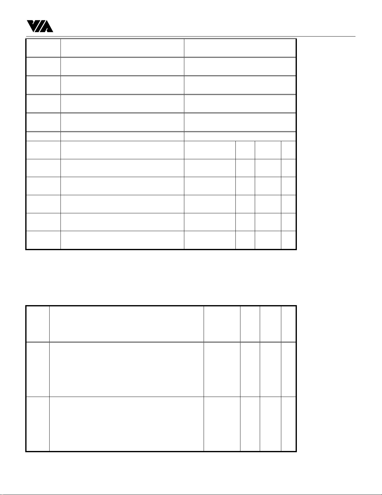
VIA Technologies, Inc. Preliminary VT6516 Datarsheet
5000H MAC & I/O Control Module of Port
as same as Port 0
11
5400H MAC & I/O Control Module of Port
as same as Port 0
12
5800H MAC & I/O Control Module of Port
as same as Port 0
13
5C00H MAC & I/O Control Module of Port
as same as Port 0
14
6000H MAC & I/O Control Module of Port
as same as Port 0
15
6400H CPU IO Control Module
00H CPU packet read byte count register bits
PKT_BYTE_CNT[7:0] 0 R/O
[7:0]
01H CPU packet read byte count register bits
PKT_BYTE_CNT[10:8]0 R/O
[10:8]
02H CPU packet read status register RD_PKT_STA
[1:0] 0 R/O
TUS
03H Packet source port ID PKT_SRC_PORT[3:0] 0 R/O
04H CPU IO port configuration register CPUIO_CFG [1:0] 0 R/
W
10H CPU packet write status register WR_PKT_STA
[2:0] 0 R/O
TUS
4. DETAIL OF SWITCH REGISTER
4.1 Registers of SDRAM Control Module
* Base Address: 0000H
Addres
s
(offset
)
00H
01H
Function Register
SDRAM TYPE:
0: 16Mbit SDRAM chip (default)
1: 64Mbit
This register has to be specified before initialization of the buffer
control because the Bank 1 free buffer pointer should have initial
value 130 for 16Mbit SDRAM, or, initial value 131 for 64Mbit
SDRAM.
CAS Latency for read operation:
2’b00: latency 1
2’b01: latency 2
2’b10: latency 3 (default)
This latency specifies the required delay between the CAS cycle and
the first read cycle. Note that the CAS latency has to be specified
before using RSDM in SDRAM initialization.
Name
Bits Defau
lt
R/
W
Value
SDRAMTYPE [0] 0 R/W
CL [1:0] 2 R/W
-44-
Page 45
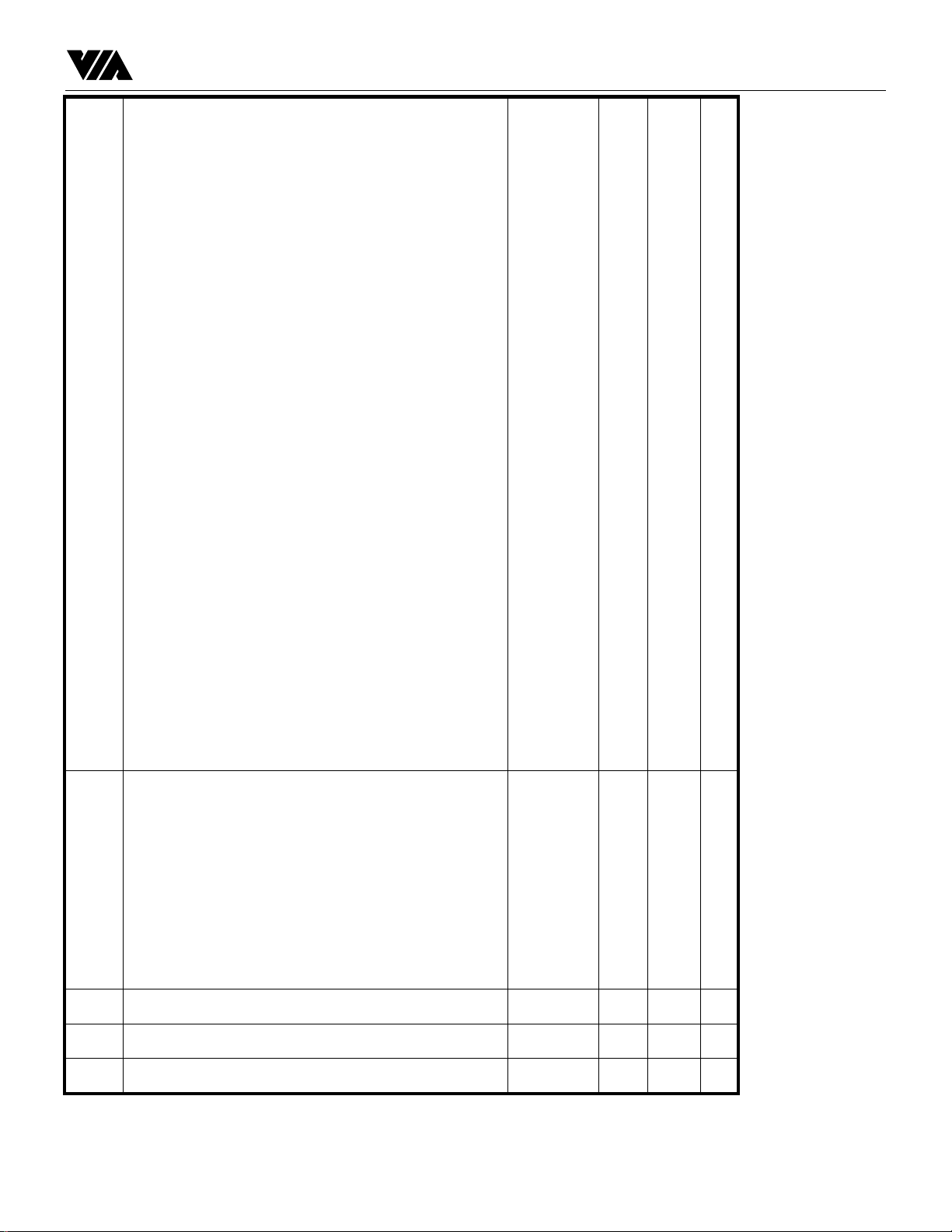
VIA Technologies, Inc. Preliminary VT6516 Datarsheet
02H
03H
SDRAM Operation Mode:
For the bits [2:0], the operation modes are defined as follows:
3’b000: Normal SDRAM Mode
3’b001: NOP Command Enable
3’b010: Precharge All Banks
3’b011: MSR Enable (Mode Register Set Enable)
3’b100: CBR Refresh Cycle Enable
others: idle for power-up
For the bit [3], it is called REFRESH_EN, defined as follows:
0: turn off hardware refresh cycle (default)
1: turn on hardware refresh cycle
After the last refresh operation issued by software in the
initialization cycle, software should enable the bit “REFRESH_EN”
immediately to notify SDRAM control module ‘sdramctl’ to start
generating refresh cycle periodically.
The initialization of SDRAM control module is illustrated as
follows:
SDRAMTYPE ß 0 : 16Mb
CL ß 1 : read latency = 2
(3) delay 1 s
(4) RSDM ß 1 : NOP
(5) delay 1 s
(6) RSDM ß 2 : Precharge
(7) delay 1 s
(8) loop 7 times
RSDM ß 4 : Refresh
delay 1 s
RSDM ß 1 : NOP
delay 1 s
(9) RSDM ß 0CH : Refresh & turn on hardware refresh
(10) delay 1 s
(11) RSDM ß 0BH : Mode Register Set Enable
(12) delay 1 s
(13) RSDM ß 08H : Normal SDRAM Mode
(14) END0A ß 0x04 : DIM bank 0 ending address = 32MB
(15) END1A ß 0x08 : DIM bank 1 ending address = 64MB
(16) END2A ß 0x0C : DIM bank 2 ending address = 96MB
(17) END3A ß 0x10 : DIM bank 3 ending address = 128MB
Bits [27:23] of DIMM Bank 0 Ending Address
RSDM [3:0] 5 R/W
END0A [4:0] 0 R/W
04H
05H
06H
For the case that there are two 32MB SDRAM modules plugged in
DIMM slot 0 and two 16MB SDRAM modules plugged in DIMM
slot 1, assign the registers as follows
END0A = 04H to indicate the ending address of DIMM Bank 0 is at
2^25 (32MB)
END1A = 08H to indicate the ending address of DIMM Bank 1 is at
2^26 (64MB)
END2A = 0AH to indicate the ending address of DIMM Bank 0 is at
2^26+2^24 (80MB)
END3A = 0CH to indicate the ending address of DIMM Bank 0 is at
2^26+2^25 (96MB)
Bits [27:23] of DIMM Bank 1 Ending Address
(see END0A)
Bits [27:23] of DIMM Bank 2 Ending Address
(see END0A)
Bits [27:23] of DIMM Bank 3 Ending Address
(see END0A)
-45-
END1A [4:0] 0 R/W
END2A [4:0] 0 R/W
END3A [4:0] 0 R/W
Page 46
VIA Technologies, Inc. Preliminary VT6516 Datarsheet
07H
08H
SDRAM Command Drive Strength Configure
bit0: RDCSDV --- SDRAM Chip Select Drive Strength
bit1: RMADV --- SDRAM MA drive strength
(including RAS,CAS,WE,MA,BA)
bit2: RMDDV --- SDRAM MD drive strength
SDRAM Bank Interleaving Disable
0: enable interleaving (default)
1: disable interleaving
4.2 Registers of SRAM Control Module
* Base Address: 0800H
Addres
Function Register
s
(offset
)
00H SRAM Read Command Interleave Disable
0: enable interleaving (default)
1: disable interleaving
4.3 Registers of Queue Control Module
SDRAM_DR_
CFG
BK_IL_DIS [0] 0 R/W
Name
[2:0] 0 R/W
Bits Defau
lt
R/
W
Value
SRAM_READ
_IL_DIS
[0] 0 R/W
* Base Address: 0C00H
Addres
Function Register
s
(offset
)
0002H
03H
Free Memory Flow Control Threshold register
As FREEMCNT(a register in buffer control) < FMFCT, the
congestion control function will be triggered to command the TMAC
module of the source port, destined to a congested port, to send out
a flow control frame for full duplex mode, or to make back-pressure
for half duplex mode. See the context about congestion control for
details.
Larger the threshold value more sensitive the congestion control
mechanism, i.e. maybe poor utilization for packet buffers but larger
packet loss rate. Smaller the threshold value less sensitive the
congestion control mechanism, i.e. maybe good utilization for
packet buffers but smaller packet loss rate. It depends on the
network configuration and traffic pattern. The recommended
threshold value is 256.
Cut Through Enable
0: Disable Cut Through (default)
1: Enable Cut Through
Note: REMEMBER to enable the cut-through function to improve
the switching latency. For 100Mbps input port, the smallest latency
for cut-through is 288 bytes time (288x8x10 ns). For 10Mbps input
port, the smallest latency for cut-through is 96 bytes time (96x8x100
ns).
Name
FMFCT
CUT_THROU
GH_EN
Bits Defau
lt
R/
W
Value
[18:0]0 R/
W
[0] 0 R/W
-46-
Page 47
VIA Technologies, Inc. Preliminary VT6516 Datarsheet
04H
1013H
1417H
181BH
1C1FH
2023H
2427H
282BH
2C2FH
3033H
3437H
383BH
3C3FH
4043H
4447H
484BH
CPU Port Speed Configuration
3’b000: 1 Mbit (default)
3’b001: 5 Mbit
3’b010: 10 Mbit
3’b011: 20 Mbit
3’b100: 40 Mbit
3’b101: 50 Mbit
3’b110: 80 Mbit
3’b111: 100 Mbit
This register is used to calculate the congestion factor of the CPU
port, that is the quotient of the accumulated byte count of the CPU
output queue to the specified CPU port speed. While the congestion
control is triggered, the output ports with congestion factor larger
than the average will enter into the congestion control mode.
Congestion Factor of Output Port 0
The congestion factor, i.e. the quotient of the accumulated byte
count of the output queue to the port speed, for each of 16 Ethernet
ports is calculated by the flow control module. While the congestion
control is triggered, the output ports with congestion factor larger
than the average will enter into the congestion control mode.
Congestion Factor of Output Port 1 CONGEST_F
Congestion Factor of Output Port 2
Congestion Factor of Output Port 3
Congestion Factor of Output Port 4
Congestion Factor of Output Port 5
Congestion Factor of Output Port 6
Congestion Factor of Output Port 7
Congestion Factor of Output Port 8
Congestion Factor of Output Port 9
Congestion Factor of Output Port 10
Congestion Factor of Output Port 11
Congestion Factor of Output Port 12
Congestion Factor of Output Port 13
Congestion Factor of Output Port 14
CPU_SPD_CFG[2:0] 0 R/W
CONGEST_F
CT0
CT1
CONGEST_F
CT2
CONGEST_F
CT3
CONGEST_F
CT4
CONGEST_F
CT5
CONGEST_F
CT6
CONGEST_F
CT7
CONGEST_F
CT8
CONGEST_F
CT9
CONGEST_F
CT10
CONGEST_F
CT11
CONGEST_F
CT12
CONGEST_F
CT13
CONGEST_F
CT14
[25:0] 0 R/O
[25:0] 0 R/O
[25:0] 0 R/O
[25:0] 0 R/O
[25:0] 0 R/O
[25:0] 0 R/O
[25:0] 0 R/O
[25:0] 0 R/O
[25:0] 0 R/O
[25:0] 0 R/O
[25:0] 0 R/O
[25:0] 0 R/O
[25:0] 0 R/O
[25:0] 0 R/O
[25:0] 0 R/O
-47-
Page 48
VIA Technologies, Inc. Preliminary VT6516 Datarsheet
4C-
Congestion Factor of Output Port 15
4FH
5053H
Congestion Factor of Output Port 16 (CPU port)
There are 11 bits are used for reading FREEMCNT. Only 15 bits are
used as CPU port’s congestion factor. The read sequence of
CONGEST_FCT16[14:0] is as follows:
1. Read 0C50H to get the lowest byte.
CONGEST16[7:0] = HD[7:0]
2. Read 0C51H to get the other 7 bits.
CONGEST16[14:8] = HD[6:0]
4.4 Registers of Buffer Control Module
* Base Address: 1000H
Addres
Function Register
s
(offset
)
00-02H
03-05H
0608H
Bank 0 Free Pointer
This register is initialized according to SDRAMTYPE while the
CFP is written. For 16/64Mbit SDRAM, its value is always 128
because the bank 0 free list follows the private buffer pool of buffer
entries 0~127. The free buffers with starting address at the SDRAM
even bank should be linked into this free list to improve the SDRAM
bandwidth utilization. However, if the free buffers are misplaced,
they will returned to the adequate free lists after their first release by
the output port control. Internally, the free pointer refers to the ID of
the 1st free buffer, rather than its physical address in SRAM (that is
equal to ID*3).
Bank 1 Free Pointer
This register is initialized according to SDRAMTYPE while the
CFP is written. For 16Mbit SDRAM, its value is 130. For 64Mbit
SDRAM, its value is 131. The fixed buffer size is 1536 bytes.
Because the page size is 2KB for 16Mbit SDRAM, the first public
buffer of bank 1 is the 130th entry located at page 1. Because the
page size is 4KB for 64Mbit SDRAM, the first public buffer of bank
1 is the 131st entry located at page 1.
Free Memory Block Count
It is an integer value <= sizeof(SDRAM) / 1.5KB. It has to be
specified at the switch initialization stage.
To fix the bug of reading FREEMCNT in VT3061A, the bit
mapping for reading FREEMCNT is modified in VT3061B.
The write sequence of FREEMCNT is also to write data to
1006H, 1007H, 1008H. However, the read sequence of
FREEMCNT has to read data from
(1) Read 1006H to get the lowest byte, and also lock the
counter information, .i.e. FREEMCNT[7:0] = HD[7:0]
(2) Read 0C52H to get the second byte, i.e.
FREEMCNT[15:8] = HD[7:0]
(3) Read 0C53H to get the FREEMCNT[17:16]
FREEMCNT[17:16] = HD[1:0]
(4) Read 0C51H to get the FREEMCNT[18]
FREEMCNT[18] = HD[7]
CONGEST_F
CT15
CONGEST_F
CT16
[25:0] 0 R/O
[25:0] 0 R/O
Bits Defau
Name
FREE0_PT [18:0
]
FREE1_PT [18:0
]
FREEMCNT[18:0
]
lt
Value
R/
W
R/O
R/O
R/
W
-48-
Page 49
VIA Technologies, Inc. Preliminary VT6516 Datarsheet
09H
10H
11H
12H
13H
14H
15H
16H
17H
18H
19H
1AH
1BH
1CH
1DH
1EH
1FH
CLEAR All Free Pointers
Write to this register will reset the two free buffer pointers
according to the SDRAMTYPE. It is the only way to program the
FREE0_PT and FREE1_PT. This command should be taken after
the SDRAMTYPE has been specified.
PRIVATE MEMORY ALLOCATION BIT MASK for PORT 0
Each bit corresponds to a private packet buffer. This mask register
will be cleared to bit pattern 0000-0000 while system reset. The 8
private buffers for the port K are that of entry IDs (K*8) ~ (K*8+7).
But, the CPU IO port has not private buffers.
PRIVATE MEMORY ALLOCATION BIT MASK for PORT 1
PRIVATE MEMORY ALLOCATION BIT MASK for PORT 2
PRIVATE MEMORY ALLOCATION BIT MASK for PORT 3
PRIVATE MEMORY ALLOCATION BIT MASK for PORT 4
PRIVATE MEMORY ALLOCATION BIT MASK for PORT 5
PRIVATE MEMORY ALLOCATION BIT MASK for PORT 6
PRIVATE MEMORY ALLOCATION BIT MASK for PORT 7
PRIVATE MEMORY ALLOCATION BIT MASK for PORT 8
PRIVATE MEMORY ALLOCATION BIT MASK for PORT 9
PRIVATE MEMORY ALLOCATION BIT MASK for PORT
10
PRIVATE MEMORY ALLOCATION BIT MASK for PORT
11
PRIVATE MEMORY ALLOCATION BIT MASK for PORT
12
PRIVATE MEMORY ALLOCATION BIT MASK for PORT
13
PRIVATE MEMORY ALLOCATION BIT MASK for PORT
14
PRIVATE MEMORY ALLOCATION BIT MASK for PORT
15
CFP [0] W/
O
PORT0_M
[7:0] 0 R/O
ASK
PORT1_M
[7:0] 0 R/O
ASK
PORT2_M
[7:0] 0 R/O
ASK
PORT3_M
[7:0] 0 R/O
ASK
PORT4_M
[7:0] 0 R/O
ASK
PORT5_M
[7:0] 0 R/O
ASK
PORT6_M
[7:0] 0 R/O
ASK
PORT7_M
[7:0] 0 R/O
ASK
PORT8_M
[7:0] 0 R/O
ASK
PORT9_M
[7:0] 0 R/O
ASK
PORT10_
[7:0] 0 R/O
MASK
PORT11_
[7:0] 0 R/O
MASK
PORT12_
[7:0] 0 R/O
MASK
PORT13_
[7:0] 0 R/O
MASK
PORT14_
[7:0] 0 R/O
MASK
PORT15_
[7:0] 0 R/O
MASK
4.5 Registers of Forwarding Control Module
-49-
Page 50

VIA Technologies, Inc. Preliminary VT6516 Datarsheet
* Base Address: 1400H
Addres
s
(offset
)
00H
0103H
04H
Function Register
bits of MAC address used as index for forwarding table
3’b000: use MAC address bit 10-0 (default)
3’b001: use MAC address bit 11-0
3’b010: use MAC address bit 12-0
3’b011: use MAC address bit 13-0
3’b100: use MAC address bit 14-0
others, use MAC address bit 10-0
This register specifies the lookup hash key. For example, if the
MAC address bits [14:0] is used as the hash key, there must be 32K
96-byte table entries necessary to be allocated in the upper part of
SRAM for destination MAC lookup and source MAC learning.
starting SRAM address register for forwarding table base
The forwarding table should be located above the linked buffer
entries in the SRAM. The starting address of the forwarding table is
specified by TBL_BASE in unit of 32-bit word. The occupied size is
determined by HASH_BITS. For example, if there are maximum
5461 buffers entries used for 8MB SDRAM, the minimum
forwarding table base is 5461*3 because each linked buffer entry is
of size 96 bits (3 words).
user configured Forwarding Mode
bit 0 – if using the specified forwarding mask without lookup
(default: 0, to take lookup without specified mask)
bit 1 – if not forwarding packets destined to congested ports
(default: 0, not to filter packets by congestion factors)
Name
Bits Defau
lt
R/
W
Value
HASH_BITS [2:0] 0 R/W
TBL_BASE [18:0] 0 R/W
FWD_MODE [1:0] 0 R/W
0507H
0809H
If FWD_MODE[0] = 1, the incoming packets would not be
forwarded with table lookup. However, the USER_PM is used as
the forwarding mask if the incoming packets are not from the CPU
port. For broadcast & lookup-miss packets, the USER_PM is
returned by Forwarding Control to IO Control as the lookup result.
If FWD_MODE[1] = 1, the incoming packets would not be
forwarded to the congested ports whose congestion factors are larger
than 511.
USER configured Port Mask
The USER_PM is used as the lookup result for the incoming packets
from Ethernet ports in the following cases:
FWD_MODE = 1
FWD_MODE = 0, VLAN is off, STP_STATE is “forward”, and this
is a broadcast packet or a lookup-miss packet
port mask for packets sent by CPU
The CPU_PM is used as the lookup result for the incoming packets
from the CPU port without regard to packet’s DMAC.
USER_PM [16:0] 0 R/W
CPU_PM [15:0] 0 R/W
-50-
Page 51
VIA Technologies, Inc. Preliminary VT6516 Datarsheet
0AH
0BH
0C-0EH
10H
CPU port related forwarding configuration
bit 0 – enable forwarding broadcast packets with
DMAC=0xffffffffffff to CPU
(default = 0 : disable)
bit 1 – enable forwarding spanning-tree packets to CPU
(default = 0 : disable)
bit 2 – enable forwarding unicast packets with DMAC =
switch MAC base to CPU
(default = 0 : disable)
The three register bits are used to enable/disable forwarding the
above three types of frames to the CPU port. Note that for a
lookup-miss packet, whether it will be forwarded to the CPU port is
determined by the bit USER_PM[16], rather than this register.
Sniffer Port ID
This register is valid only if MONITOR_PM is not all 0's. The
default value of MONITOR_PM is all 0's to disable the Sniffer
function.
Monitor Port Mask
This register is used to specify which ports to be monitored by
Sniffer so that all packets forwarded from/to the monitored ports are
also made a copy sent to the Sniffer port. The Sniffer function is
enabled only if MONITOR_PM is not all 0's. The default value of
MONITOR_PM is all 0's to disable the sniffer function.
high byte [14:8] of the MAC hash address to be aged
CPU_FWD_CFG[2:0] 0 R/W
SNIFFER_PID [3:0] 0 R/W
MONITOR_PM[16:0] 0 R/W
AGE_MAC [6:0] 0 R/W
11H
12H
AGE_MAC is in the hash-key format of bits [14:0]. The high byte
[14:8] is stored in the AGE_MAC register of offset 10H. The low
byte [7:0] is stored in the AGE_MAC register of offset 11H. A write
to the register of offset 11H will trigger an aging operation that
decreases by one the age count of the corresponding forwarding
table entry. A forwarding table entry with age count = 0 is an invalid
entry, i.e. this entry is available for the source MAC learning.
AGE_MAC is reset to all 0's after aging.
low byte [7:0] of the MAC hash address to be aged
(see the above)
Aging Status
0, idle or done (default)
1: aging in progress
After an aging command is issued, the status is recorded in this
register. The next age command can only be issued as the status
changes from 1 (in-progress) to 0 (done).
AGE_MAC [7:0] 0 R/W
AGING_STATUS[0] 0 R/O
-51-
Page 52
VIA Technologies, Inc. Preliminary VT6516 Datarsheet
20H
21H
22H
23H
24H
25H
26H
27H
28H
29H
2AH
2BH
2CH
2DH
2EH
2FH
80H
spanning tree state for PORT 0
2’b00 – blocking state (default)
2’b01 – listening state
2’b10 - learning state
2’b11 – forwarding state
The forwarding operation in each Ethernet port is controlled by its
associated spanning tree state.
In blocking or listening state, the incoming packets will not trigger
any DMAC lookup operation and SMAC learning operation.
In learning state, the incoming packets will not trigger DMAC
lookup operation, but the SMAC learning operation will be
triggered for CRC-OK packets.
Only in forwarding state, an incoming packet will trigger DMAC
lookup operation while the first 24 bytes are received, and it will
trigger the SMAC learning operation while the whole packet is
received with good CRC.
For the 802.1d spanning tree algorithm, a blocked port for loop
avoidance should enter the blocking state so that any incoming
packets are filtered without forward. A normal port that does not
cause any loop should be in the forwarding state.
spanning tree state for PORT 1
spanning tree state for PORT 2
spanning tree state for PORT 3
spanning tree state for PORT 4
spanning tree state for PORT 5
spanning tree state for PORT 6
spanning tree state for PORT 7
spanning tree state for PORT 8
spanning tree state for PORT 9
spanning tree state for PORT 10
spanning tree state for PORT 11
spanning tree state for PORT 12
spanning tree state for PORT 13
spanning tree state for PORT 14
spanning tree state for PORT 15
port 0 VLAN ID
PORT0_STP_
STATE
PORT1_STP_
STATE
PORT2_STP_
STATE
PORT3_STP_
STATE
PORT4_STP_
STATE
PORT5_STP_
STATE
PORT6_STP_
STATE
PORT7_STP_
STATE
PORT8_STP_
STATE
PORT9_STP_
STATE
PORT10_STP
_STATE
PORT11_STP
_STATE
PORT12_STP
_STATE
PORT13_STP
_STATE
PORT14_STP
_STATE
PORT15_STP
_STATE
PORT0_VID [5:0] 0 R/W
[1:0] 0 R/W
[1:0] 0 R/W
[1:0] 0 R/W
[1:0] 0 R/W
[1:0] 0 R/W
[1:0] 0 R/W
[1:0] 0 R/W
[1:0] 0 R/W
[1:0] 0 R/W
[1:0] 0 R/W
[1:0] 0 R/W
[1:0] 0 R/W
[1:0] 0 R/W
[1:0] 0 R/W
[1:0] 0 R/W
[1:0] 0 R/W
82H
84H
86H
88H
The VLAN feature is enabled only when all port VID's are
configured to a valid (non-zero) VID.
port 1 VLAN ID PORT1_VID [5:0] 0 R/W
port 2 VLAN ID PORT2_VID [5:0] 0 R/W
port 3 VLAN ID PORT3_VID [5:0] 0 R/W
port 4 VLAN ID PORT4_VID [5:0] 0 R/W
-52-
Page 53
VIA Technologies, Inc. Preliminary VT6516 Datarsheet
8AH
8CH
8EH
90H
92H
94H
96H
98H
9AH
9CH
9EH
A0A1H
port 5 VLAN ID PORT5_VID [5:0] 0 R/W
port 6 VLAN ID PORT6_VID [5:0] 0 R/W
port 7 VLAN ID PORT7_VID [5:0] 0 R/W
port 8 VLAN ID PORT8_VID [5:0] 0 R/W
port 9 VLAN ID PORT9_VID [5:0] 0 R/W
port 10 VLAN ID PORT10_VID [5:0] 0 R/W
port 11 VLAN ID PORT11_VID [5:0] 0 R/W
port 12 VLAN ID PORT12_VID [5:0] 0 R/W
port 13 VLAN ID PORT13_VID [5:0] 0 R/W
port 14 VLAN ID PORT14_VID [5:0] 0 R/W
port 15 VLAN ID PORT15_VID [5:0] 0 R/W
Server Port Mask
The SRV_PM is used only when VLAN is enabled. As the VLAN
feature is enabled (i.e. all port VID’s are valid (non-zero)), the
behavior is described for the following scenarios:
A broadcast or lookup-miss packet will be forwarded to the ports of
same VLAN ID. If CPU_FWD_CFG[0]=1, the broadcast packet will
also be forwarded to CPU port.
A unicast packet destined to different VLAN will be forwarded to
CPU port if VLAN_FWD_CFG[0]=1.
A unicast packet destined to another port in the same VLAN will be
forwarded in a unicast manner.
SRV_PM [15:0] 0 R/W
The SRV_PM should be set for the Server ports that respond to carry
cross VLAN packets. It is recommended that all packets from the
Server stations have not any embedded VID. Only the cross VLAN
packets through the Server ports (the corresponding SRV_PM bits
are on) within different VLAN domain must carry VID.
In the source-MAC learning procedure, for packets with tagged
VID, the corresponding forwarding table entry will have NOT the
tagging bit on to make the outgoing packets destined to it with VID
tagged. All valid forwarding table entries should have non-zero
VID.
A2H
VLAN related forwarding configuration
This register bit is used to enable those packets destined to a
different VLAN also to be forwarded to the CPU port.
This scenario happens when the following conditions hold
simultaneously:
The destination MAC address is found in forwarding table (lookup
hit), and this entry is not static. Note that if the entry is static, its
priority is highest and the destination ports are fully determined by
the port mask field in the entry so that forwarding to CPU is not
necessary.
The source VID differs from the destination VID.
4.6 Registers of PHY Control Module
VLAN_FWD_
CFG
[0] 0 R/W
* Base Address: 1800H
-53-
Page 54
VIA Technologies, Inc. Preliminary VT6516 Datarsheet
Addres
s
(offset
)
00H
01H
0203H
04H
05H
Function Register
Name
PHY ID
This is used to specify which PHY device is the objective of the
following MII commands. There are maximum 16 RMII PHY
devices.
PHY register address
In each PHY device, there are maximum 32 MII management
registers accessible by the CPU. The PHY_REG_ADDR register is
used to specify which one is the objective of the following access
command.
PHY data register
Each PHY management register is 16 bits. Every data access to a
PHY management register is in unit of 16 bits, stored in this
register.
PHY command register
1: read
0: write
Write 0 to this register will cause a write operation to the PHY
management register (specified by the PHY_REG_ADDR) of the
PHY device (specified by the PHYID). Write 1 to this register will
cause a read operation. A read or write operation takes about 0.4 ms
so that the CPU has to read the PHYSTS register periodically to
check if the issued command is complete.
PHY status register
2’b00: idle
2’b01: busy
2’b10: complete
PHYID [3:0] 0 W/
PHY_REG
_ADDR
PHYDATA[15:0
PHYCMD [0] W/
PHYSTS [1:0] 0 R/O
Bits Defau
lt
R/
W
Value
O
[4:0] 0 W/
O
R/
]
W
O
10H
11H
12H
This register indicates the status of the PHY control module.
Initially, the PHY control module is in the idle status. While a read
or write command is issued by writing 1/0 to the PHYCMD register,
PHYSTS becomes “busy” immediately, and goes into the
“complete” status as this operation finishes. Then, a following “read
status” command will cause it back to the “idle” status, or a
following read/write command will cause it into the “busy” status.
PORT0 PHY Device Address
The pair of 5-bit PHY device address and 5-bit register address
forms a unique access address to a PHY device’s register. Each PHY
device has a unique device address that is identified by the PHYID.
In the system initialization, the CPU should write PHY device
addresses, corresponding to every PHY devices, to registers
PORT[0..15]_PHY_ADDR, that may be recorded in the EEPROM
or code ROM.
PORT1 PHY Device Address
PORT2 PHY Device Address
-54-
PORT0_P
HY_ADD
R
PORT1_P
HY_ADD
R
PORT2_P
HY_ADD
R
[4:0] 0 R/
W
[4:0] 0 R/
W
[4:0] 0 R/
W
Page 55

VIA Technologies, Inc. Preliminary VT6516 Datarsheet
13H
14H
15H
16H
17H
18H
19H
1AH
1BH
1CH
1DH
1EH
1FH
PORT3 PHY Device Address
PORT4 PHY Device Address
PORT5 PHY Device Address
PORT6 PHY Device Address
PORT7 PHY Device Address
PORT8 PHY Device Address
PORT9 PHY Device Address
PORT10 PHY Device Address
PORT11 PHY Device Address
PORT12 PHY Device Address
PORT13 PHY Device Address
PORT14 PHY Device Address
PORT15 PHY Device Address
PORT3_P
HY_ADD
R
PORT4_P
HY_ADD
R
PORT5_P
HY_ADD
R
PORT6_P
HY_ADD
R
PORT7_P
HY_ADD
R
PORT8_P
HY_ADD
R
PORT9_P
HY_ADD
R
PORT10_P
HY_ADD
R
PORT11_P
HY_ADD
R
PORT12_P
HY_ADD
R
PORT13_P
HY_ADD
R
PORT14_P
HY_ADD
R
PORT15_P
HY_ADD
R
[4:0] 0 R/
W
[4:0] 0 R/
W
[4:0] 0 R/
W
[4:0] 0 R/
W
[4:0] 0 R/
W
[4:0] 0 R/
W
[4:0] 0 R/
W
[4:0] 0 R/
W
[4:0] 0 R/
W
[4:0] 0 R/
W
[4:0] 0 R/
W
[4:0] 0 R/
W
[4:0] 0 R/
W
4.7 Registers of EEPROM Control Module
* Base Address: 1C00H
-55-
Page 56
VIA Technologies, Inc. Preliminary VT6516 Datarsheet
Addres
s
(offset
)
00H
01H
02H
03H
Function Register
Name
EEPROM word address
For a 256-byte EEPROM device, an 8-bit data object is identified
with this register. For a 512-byte EEPROM device, an 8-bit data
object is identified with this register plus EEDEVADDR[1]. For a
1024-byte EEPROM device, an 8-bit data object is identified with
this register plus EEDEVADDR[2:1], vice versa.
EEPROM data
Every data access to EEPROM is in unit of 8 bits, stored in this
register.
EEPROM device address
bit 7-4 : device type id (EEPROM 1010)
bit 3-1 : device id
bit 0 : r/w command , value 0: write; value 1: read
The triple of 4-bit PHY device type ID, 3-bit device ID, and 7-bit
word address forms a unique access address to an 8-bit EEPROM
data object.
This register’s bit 0 is used to specify the command type: 0 for write
and 1 for read. A read or write operation takes about 0.4 ms so that
the CPU has to read the EEYSTS register periodically to check if the
issued command is “complete without error” or “ack error”.
EEPROM status register
3’b000: idle
3’b001: busy
3’b010: complete without error
3’b100: ack error
EEWDADDR[7:0] W/
EEDATA [7:0] R/
EEDEVA
DDR
EESTS [2:0] R/O
Bits Defau
lt
R/
W
Value
O
W
[7:0] W/
O
This register indicates the status of the EEPROM control module.
Initially, the EEPROM control module is in the idle status. While a
read or write command is issued by writing 1/0 to EEDEVADDR[0],
EESTS becomes “busy” immediately, and goes into the “complete”
status as this operation finishes or into the “ack error” as an
acknowledge error happens. Then, a following “read status”
command will cause it back to the “idle” status, or a following
read/write command will cause it into the “busy” status.
4.8 Registers of CPU Interface Module
* Base Address: 2000H
Addres
Function Register
s
(offset
)
Name
Bits Defau
lt
Value
R/
W
-56-
Page 57

VIA Technologies, Inc. Preliminary VT6516 Datarsheet
00H
01H03H
04H07H
08H
09H
10H13H
14H1BH
1CH
interrupt status register
bit 0: interrupt indication for read/write PHY command
complete
bit 1: interrupt indication for read/write EEPROM command
complete or error
bit 2: interrupt indication for CPU IO port receiving an
incoming packet
bit 3: interrupt indication for CPU IO port finishing the
transmission of an outgoing packet
To clear an interrupt, write 1 to the corresponding IRQSTS bit.
However, write 0 will not cause any change on that interrupt.
SRAM address register
The data object addressed is in unit of 32 bits. The maximum
allowable SRAM size is 1MB. For SRAM direct access, the CPU
has to (1) set SRAMADDR & SRAMDATA, (2) issue read/write
command by SRAMCMD, and (3) check command status by
SRAMSTS.
SRAM data register
SRAM command register
2’b00 : nop
2’b01 : read
2’b10 : write
To make a direct read to SRAM, write SRAMCMD by 2’b01. To
make a direct write to SRAM, write SRAMCMD by 2’b10.
Read/Write will cause the SRAMSTS = ”busy” immediately. As it is
done, SRAMSTS = “done”. A following read to SRAMSTS will
clear it to “idle”.
SRAM status register
2’b01 : read/write command done
2’b10 : busy (read/write in progress)
2’b00 : idle
SDRAM address register
The data object addressed is in unit of 64 bits. The maximum
allowable SDRAM size is 128MB. For SDRAM direct access, the
CPU has to (1) set SDRAMADDR & SDRAMDATA, (2) issue
read/write command by SDRAMCMD, and (3) check command
status by SDRAMSTS.
SDRAM data register
SDRAM command register
2’b00 : nop
2’b01 : read
2’b10 : write
IRQSTS [3:0] 0 R/
W
SRAMADDR[18:0
]
SRAMDATA[31:0
]
R/
W
R/
W
SRAMCMD[1:0] R/
W
SRAMSTS [1:0] 0 R/O
SDRAMA
DDR
SDRAMD
ATA
[23:0
]
[63:0
]
R/
W
R/
W
SDRAMCMD[1:0] R/
W
1DH
To make a direct read to SDRAM, write SDRAMCMD by 2’b01. To
make a direct write to SDRAM, write SDRAMCMD by 2’b10.
Read/Write will cause the SDRAMSTS = ”busy” immediately. As it
is done, SDRAMSTS = “done”. A following read to SDRAMSTS
will clear it to “idle”.
SDRAM status register
2’b01 : read/write command done
2’b10 : busy (read/write in progress)
2’b00 : idle
-57-
SDRAMSTS[1:0] 0 R/O
Page 58

VIA Technologies, Inc. Preliminary VT6516 Datarsheet
20H
21H
30H
31H
32H
33H
34H
35H
40H
Write packet command
3’b100 : end of frame with the remaining data size = 2 bytes
3’b101 : end of frame with the remaining data size = 1 byte
(that is the low byte as using 16-bit write)
3’b000 : idle
3’b001 : start of frame for the next write
3’b010 : middle of frame for the next write
3’b011 : abort the unfinished packet write
CPU should write this command register before repeatedly writing
8/16 bit packet data VIA the ISA/IDE bus (with a2, a1, a0 = 000).
Packet Abort
Write this register to drop an incoming packet ready to be read by
CPU.
bits [47:40] of switch base MAC address [47:0]
Each port in the switch IC has a unique MAC address with the port
ID as address bits [3:0] and the same MAC base bits [47:4],
specified by the register SWITCH_MAC_BASE[47:4].
bits [39:32] of switch base MAC address [47:0]
bits [31:24] of switch base MAC address [47:0]
bits [23:16] of switch base MAC address [47:0]
bits [15:8] of switch base MAC address [47:0]
bits [7:4] of switch base MAC address [47:0]
interrupt mask register
bit 0: PHY interrupt mask
bit 1: EEPROM interrupt mask
bit 2: packet received interrupt mask
bit 3: packet sent interrupt mask
WR_PKT_
CMD
[2:0] W/
O
ERR_ABORT[0] W/
O
SWITCH_
MAC_BA
[7:0] 0 R/
W
SE
SWITCH_
MAC_BA
[7:0] 0 R/
W
SE
SWITCH_
MAC_BA
[7:0] 0 R/
W
SE
SWITCH_
MAC_BA
[7:0] 0 R/
W
SE
SWITCH_
MAC_BA
[7:0] 0 R/
W
SE
SWITCH_
MAC_BA
[7:4] 0 R/
W
SE
IRQSTS_
MASK
[3:0] 4’ b1111R/
W
The four interrupts can be masked individually. The value 0
indicates “Masked”, and value 1 (default) indicates “Unmasked”.
-58-
Page 59
VIA Technologies, Inc. Preliminary VT6516 Datarsheet
50H
51H
CPU Soft Reset for the whole switch chip reset
For Read
0: soft reset in progress
1: soft reset done
For Write,
any value will trigger the whole chip reset
The soft reset is similar to power-on reset for the
switch chip, except that it is asserted by writing any
value to this register. The CPU soft reset has to take
16 RCLK50 cycles, i.e. 320ns, to make the switch
chip being reset and ready to CPU. For 8MHz 8051
CPU that an instruction cycle is 1.5 s, it needs to
wait for 4 CPU instruction cycles to continue after
the soft reset. Or, CPU can read this register
CPU_SOFT_RESET until value 1 is returned.
Note that reading this register will not cause the
address register to increment automatically. So,
consecutively reading from 2050H to 2051H should
not be applied. That is, any reading to 2051H has to
specify the address explicitly.
Revision ID Register
This register is used to record the revision code. Its
value is 0 for the first sample ICs.
CPU_SOF
T_RESET
REVISIO
N_ID
[0] 1 R/
W
[7:0] 0 R/O
4.9 Registers of MAC/IO Control Module
* Base Address: 2400H
Addres
s
(offset
)
00H configurable preamble bytes
Function Register
This register specifies the preamble length (0..7
bytes) for outgoing packets.
-59-
Bits Defau
Name
PREAM_CFG[2:0] 7 R/
lt
Value
R/
W
W
Page 60
VIA Technologies, Inc. Preliminary VT6516 Datarsheet
01H
configurable frame gap in di bits for 1st interval
This register specifies the 1st interval of the inter-frame gap (in unit
of di bit) for outgoing packets, where the 2nd interval of the interframe gap is fixed as 16 di bits (i.e. 32 bits). The minimum interframe gate (IFG) defined in 802.3 is 96 bits (48 di bits). But for fast
transmission, many manufactures use smaller IFG (minimum is 32
bits) in practical. The allowable IFG_CFG value is 0..63 di bits.
Note that, TMAC only performs the carrier sense function during
the 1st IFG interval, rather than the whole IFG. So, for the half
duplex link, if an incoming packet arrives at the 2nd IFG interval, a
collision with the ready-to-send outgoing packet will happen.
IFG_CFG [5:0] 32 R/
W
-60-
Page 61
VIA Technologies, Inc. Preliminary VT6516 Datarsheet
nd
02H Backoff configuration
bit 0: CAP mode , mild solution for Capture effect
bit 1: MBA mode , aggressive solution for Capture
effect
bit 2: EEFAST mode , drop the 2nd collided packet
for testing
purpose, accelerate the drop event
bit 3: CRANDOM mode , use another random
algorithm
bit 4: OFSET , parameter for backoff timer
For that CAP mode is enabled, the TMAC module
will select the backoff time as b’10 or b’ 11 for the
2nd collision, i.e. the backoff time for the 2nd collision
is 2 or 3 slot times, where a slot time is 512 bits time
duration.
For that MBA mode is enabled, the TMAC will
select
backoff time for 10th collision just as that for 5
collision
backoff time for 11th collision just as that for 4
collision
backoff time for 12th collision just as that for 3
collision
backoff time for 13th collision just as that for 2
collision
backoff time for 14th collision just as that for 1
collision
backoff time for 15th collision as 0.
BOFFCFG [4:0] 5’b10
000R/W
th
th
rd
nd
st
For that EEFAST mode is enabled, the Output
Control will drop the packet immediately as the
second collision happens.
For that CRANDOM mode is enabled, the TMAC
will select the backoff time by using the alternative
random algorithm that calculates the backoff time as
that for 10th collision.
For OFSET=1, the TMAC will follow the 802.3
standard backoff algorithm. For OFSET=0, the
TMAC will select the backoff time for the 1st and 2
collision as that of the 3rd collision, i.e. the possible
the backoff time for the 1st and 2nd collision is ranged
from 0 to 7 in unit of slot time.
-61-
Page 62
VIA Technologies, Inc. Preliminary VT6516 Datarsheet
03H
MAC media type configuration
bit 0: SPD_10M , value 0: 100Mbps, value 1: 10Mbps
bit 1: HALF_DPX , 1: half duplex, 0: full duplex
bit 2: RCV_FC_DIS , 1: disable receive flow control frame
0: enable receive flow control frame
bit 3: XMT_FC_DIS , 1: disable send flow control frame
0: enable send flow control frame
04H IO port enable
bit 0: input port enable , 1: input enable, 0: input
disable
bit 1: output port enable , 1: output enable, 0:
output disable
10H-
received good packet count
13H
Accounting Event: receiving packets with CRC ok
and packet size between 64 and 1522 (valid
maximum packet size in spite of VLAN disabled or
enabled). Note that the RMON/MIB counter will be
locked during 4-byte continuous register-read, and
the increment (if any) is deferred until read
complete.
14H-
received bad packet count
17H
Formal Definition: "The number of inbound packets
that contained errors preventing them from being
deliverable to a higher-layer protocol."
MACCFG [3:0] 0 R/
W
IO_CFG [1:0] 0 R/
W
RCV_GO
[31:0]0 R/O
OD_PKT
RCV_BAD
[31:0]0 R/O
_PKT
18H1BH
1CH1FH
Accounting Events: (1) receiving valid-length
packets with CRC error, (2) receiving runt packets,
(3) receiving over-length packets
drop packet counter
Formal Definition: "The total number of events in
which packets were dropped by the probe due to
lack of resources. Note that this number is not
necessarily the number of packets dropped; it is just
the number of times this condition has been
detected."
Accounting Event: input FIFO overrun due to
SDRAM-bandwidth blocking or buffer starvation.
sent good packet count
Accounting Event: store-and-forward transmission
success without collision
DROP_PKT[31:0]0 R/O
XMT_GO
[31:0]0 R/O
OD_PKT
-62-
Page 63
VIA Technologies, Inc. Preliminary VT6516 Datarsheet
20H-
sent bad packet counter
23H
Formal Definition: "The number of outbound
packets that could not be transmitted because of
errors."
Accounting Event: re-transmission due to collision
or output FIFO underrun.
2800H MAC & I/O Control Module of Port 1
2C00HMAC & I/O Control Module of Port 2
3000H MAC & I/O Control Module of Port 3
3400H MAC & I/O Control Module of Port 4
3800H MAC & I/O Control Module of Port 5
3C00HMAC & I/O Control Module of Port 6
4000H MAC & I/O Control Module of Port 7
4400H MAC & I/O Control Module of Port 8
4800H MAC & I/O Control Module of Port 9
4C00HMAC & I/O Control Module of Port 10
XMT_BA
[31:0]0 R/O
D_PKT
as same as Port 0
as same as Port 0
as same as Port 0
as same as Port 0
as same as Port 0
as same as Port 0
as same as Port 0
as same as Port 0
as same as Port 0
as same as Port 0
5000H MAC & I/O Control Module of Port 11
5400H MAC & I/O Control Module of Port 12
5800H MAC & I/O Control Module of Port 13
5C00HMAC & I/O Control Module of Port 14
6000H MAC & I/O Control Module of Port 15
4.10 Registers of CPU IO Control Module
* Base Address: 6400H
Addres
Function Register
s
(offset
)
00H
01H
CPU packet read byte count register bits [7:0]
CPU can check the incoming packet length VIA the 11-bit register
PKT_BYTE_CNT [10:0] before starting to read it.
CPU packet read byte count register bits [10:8]
as same as Port 0
as same as Port 0
as same as Port 0
as same as Port 0
as same as Port 0
Bits Defau
Name
PKT_BYT
[7:0]
E_CNT
PKT_BYT
[10:8]0 R/O
E_CNT
R/
lt
W
Value
0 R/O
-63-
Page 64
VIA Technologies, Inc. Preliminary VT6516 Datarsheet
02H
CPU packet read status register
2’b00: idle or packet read in progress
2’b01: packet received successfully
2’b10: packet received with error
(CPU needs to read the same packet again)
03H Packet source port ID
CPU can check the incoming packet’s source port
ID VIA the 3-bit register PKT_SRC_PORT before
starting to read it. It is useful to the spanning tree
algorithm.
04H
10H
CPU IO port configuration register
bit 0 : input port enable , 1: input enable, 0: input disable
bit 1 : output port enable , 1: output enable, 0: output disable
CPU packet write status register
bits [1:0] : packet write status
2’b00: idle or packet write in progress
2’b01: CPU sent packet successfully
2’b10: CPU sent packet unsuccessfully
(CPU needs to re-write the packet again)
bit 2: CPU Input Control is ready for CPU to write packets
(It can be ready only after setting CPUIO_CFG[0] = 1.)
0: not ready (default)
1: ready
RD_PKT_
[1:0] 0 R/O
STATUS
PKT_SRC
[3:0] 0 R/O
_PORT
CPUIO_CFG[1:0] 0 R/
W
WR_PKT_
[2:0] 0 R/O
STATUS
-64-
Page 65
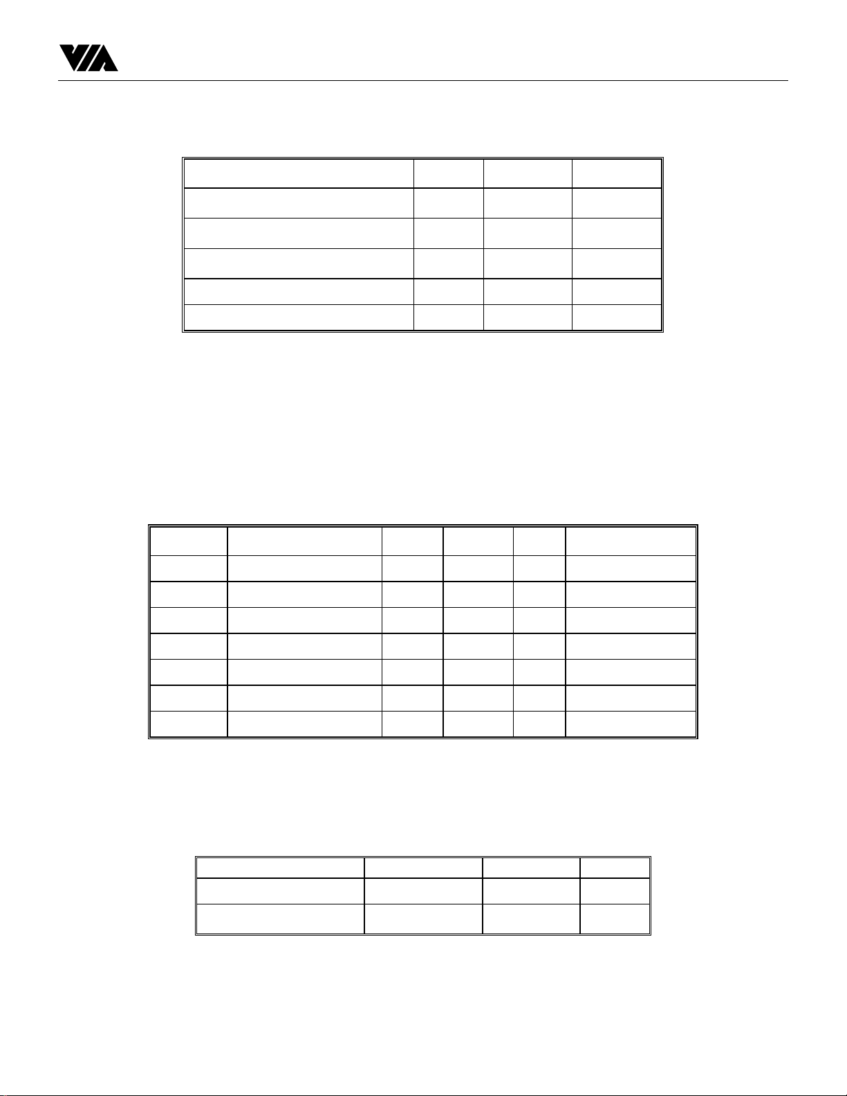
VIA Technologies, Inc. Preliminary VT6516 Datarsheet
SECTION III ELECTRICAL SPECIFICATIONS
ABSOLUTE MAXIMUM RATINGS
Parameter Min Max Unit
Ambient operating temperature 0 70 o
C
Case temperature 0 100 o
Storage temperature -55 125 o
Input voltage -0.5 5.5 Volts
Output voltage (VCC = 3.1 - 3.6V) -0.5 V
Note: Stress above the conditions listed may cause permanent damage to the
device. Functional operation of this device should be restricted to the conditions
described under operating conditions.
DC CHARACTERISTICS
TA-0-70oC, VCC=3.3V+/-5%, GND=0V
Symbol Parameter Min Max Unit Condition
V
IL
V
IH
V
OL
Input low voltage -0.50 0.8 V
Input high voltage 2.0 VCC+0.5 V
Output low voltage - 0.45 V IOL=4.0mA
+ 0.5 Volts
CC
C
C
V
OH
I
IL
I
OZ
I
CC
Output high voltage 2.4 - V IOH=-1.0mA
Input leakage current - +/-10 uA 0<VIN<V
Tristate leakage current - +/-20 uA 0.45<V
Power supply current -
TBD
mA
CC
OUT<VCC
AC CHARACTERISTICS
AC timing specifications provided are based on external zero-pf capacitance load. Min/Max cases are based on
the following table:
Parameter Min Max Unit
3.3V power (Vcc) 3.135 3.465 V
Temperature 0 95 o
-65-
C
Page 66
VIA Technologies, Inc. Preliminary VT6516 Datarsheet
- CPU interface IO Timing Characteristics
SYMBOL DESCRIPTION MIN MAX UNIT
t
IORH
t
IORL
t
VAL
t
IOWS
t
IOWH
t
IORS
t
IORH
, t
, t
IOWH
IOWL
IOR/IOW falling to
IOR/IOW rising
IOR/IOW rising to
IOR/IOW falling
HD valid to IOR/IOW
falling
IOW data setup(write
data valid to IOW
rising)
IOW data hold(IOW
rising to write data
invalid)
IOR data setup(read
data valid to IOR rising)
IOR data hold(IOW
rising to read data
invalid)
70 - ns
25 - ns
25 - ns
20 - ns
10 - ns
20 - ns
5 - ns
IOR hhhhhhhhfllllllllllrhhhhhfll
~ t
~ t
! ~t
VAL
IORH
!~ t
!~t
IORS
IORH
IORL
!
!
HD zzzzznddddddddddddddddozzzzz
CPU read timing diagram
IOWhhhhhhhhfllllllllllrhhhhhfll
~ t
~ t
! ~t
VAL
IOWH
!~ t
!~t
IOWS
IOWH
IOWL
!
!
HD zzzzznddddddddddddddddozzzzz
CPU write timing diagram
-66-
Page 67
VIA Technologies, Inc. Preliminary VT6516 Datarsheet
- SRAM interface Timing Characteristics
SYMBOL DESCRIPTION SETUP HOLD MIN MAX UNIT
t
SA
t
SDS , TSDH
t
SD
t
SADS
t
SCS
t
SWE
SCLK llrhhhhfllllrhhhhfllllrhhhflllrhhh
+ t
SADS zzzzzndddddddddozzzzzzzzznddddddd
+ t
SCS zzzzzndddddddddozzzzzzzzznddddddd
+ t
SWE zzzzzndddddddddozzzzzzzzznddddddd
+tSA~
SA zzzzndddddddddozzzzzzzzznddddddd
v input cycle v turn around cycle v output cycle v
+t
SD nddddozzzzzzzzzzzzzzzzzznddddddo
+ t
SA output delay 2 7 Ns
SD input 2.5 1.5 Ns
SD output delay 2 7 Ns
SADS output delay 2 7 Ns
SCS0 output delay 2 7 Ns
SWE output delay 2 7 ns
~
SADS
~
SCS
~
SWE
~\\ +t
SDS
~
SDH
SD
~
-67-
Page 68
VIA Technologies, Inc. Preliminary VT6516 Datarsheet
- DRAM interface Timing Characteristics
SYMBOL DESCRIPTION SETUP HOLD MIN MAX
t
MA
t
, t
MDS
MDH
t
MD
t
BA
t
RAS
t
CAS
t
DWE
t
DCS
DCLK llrhhhhfllllrhhhhfllllrhhhflllrhh
+ t
BA zzzzzndddddddddozzzzzzzzznddddddd
+ t
RAS zzzzzndddddddddozzzzzzzzznddddddd
+ t
CAS zzzzzndddddddddozzzzzzzzznddddddd
+ t
DWE zzzzzndddddddddozzzzzzzzznddddddd
+ t
DCS zzzzzndddddddddozzzzzzzzznddddddd
+tMA~
MA zzzzndddddddddozzzzzzzzznddddddd
v input cycle v turn around cycle v output cycle v
+t
MD nddddozzzzzzzzzzzzzzzzzznddddddo
+ t
MA output delay 2 6.5
MD input 1.5 2
MD output delay 2 6.5
BA0, BA1 output delay 2 6.5
RAS0, RAS1 output
delay
CAS0, CAS1 output
delay
DWE0, DWE1 output
delay
DCS3~0 output delay 2 6
2 6.5
2 6.5
2 6.5
~
BA
~
RAS
~
CAS
~
DWE
~
DCS
~\\ +t
MDS
~
NDH
MD
~
-68-
Page 69
VIA Technologies, Inc. Preliminary VT6516 Datarsheet
- RMII Interface Timing Characteristics
SYMBOL DESCRIPTION min type max unit condition
t
RC
t
RXDS
t
RXDH
t
TXD
RCLK lllrhhhhfllllrhhhhfllllrhhhhflll
+t
RXDS
CRS_DVndddddozzzndddddozzznddddddozzzz
+t
+t
RXDS
RXD ndddddozzzndddddozzznddddddozzzz
+t
+t
TX_EN zzzzzndddddddddozzzzzzzzzznddddd
+t
TXD zzzzzndddddddddozzzzzzzzzznddddd
RCLK50 cycle time 20 ns
RXD CRS_DV setup time 4 - - ns to RCLK50
RXD CRS_DV hold time 2 - - ns to RCLK50
TXD TX_EN output
delay
3 - 12 ns to RCLK50
~\\
~
RXDH
~\\
~
RXDH
~
TXD
~
TXD
rising edge
rising edge
rising edge
-69-
Page 70
VIA Technologies, Inc. Preliminary VT6516 Datarsheet
MII Interface Timing Characteristics
SYMBOL DESCRIPTION min type max unit condition
t
RC
t
RXDS
t
RXDH
t
TC
t
TXD
-
RCLK lllrhhhhfllllrhhhhfllllrhhhhflll
+t
RXDS
CRS_DVndddddozzzndddddozzznddddddozzzz
+t
+t
RXDS
RXD ndddddozzzndddddozzznddddddozzzz
+t
RCLK cycle time - 40 - ns
RXD, RXDV setup time 5 - - ns to RCLK50
RXD, RXDV hold time 5 - - ns to RCLK50
TCLK cycle time - 40 - ns
TXD, TX_EN output
delay
4 - 20 ns to RCLK50
~\\
~
RXDH
~\\
~
RXDH
rising edge
rising edge
rising edge
TCLK lllrhhhhfllllrhhhhfllllrhhhhflll
+t
TXD
~
TX_EN zzzzzndddddddddozzzzzzzzzznddddd
+t
TXD
~
TXD zzzzzndddddddddozzzzzzzzzznddddd
- Management Interface (MI) Timing Characteristics
Parameter min typ max unit condition
MDC cycle time - 400 - ns
MDC high time 180 200 220 ns
MDC low time 180 200 220 ns
MDIO setup time
(source by PHY)
MDIO hold time
(source by PHY)
30 - - ns to MDC rising
edge
0 - - ns to MDC rising
edge
MDIO output 200 - 300 ns to MDC rising
-70-
Page 71

VIA Technologies, Inc. Preliminary VT6516 Datarsheet
delay (source by
vt3061)
edge
-71-
Page 72
VIA Technologies, Inc. Preliminary VT6516 Datarsheet
- EEPROM Interface Timing Characteristics
Parameter min typ max unit condition
EEC clock
frequency
Clock high time - 6.4 -
0 78.12 - kHz
µs
Clock low time - 6.4 -
Start Condition
setup time
Start Condition
hold time
Stop Condition
setup time
Stop Condition
hold time
Read Data In
setup time
Read Data In
hold time
EEIO Data out
delay
Write Cycle time - 11.4 - ms
6.4 - -
6.4 - -
0 - - to EEC rising
0 - - to EEC falling
2.6 - 3.0
6.4 - -
6.4 - -
µs
µs
µs
µs
µs
µs
edge
edge
to EEC falling
edge
-72-
Page 73
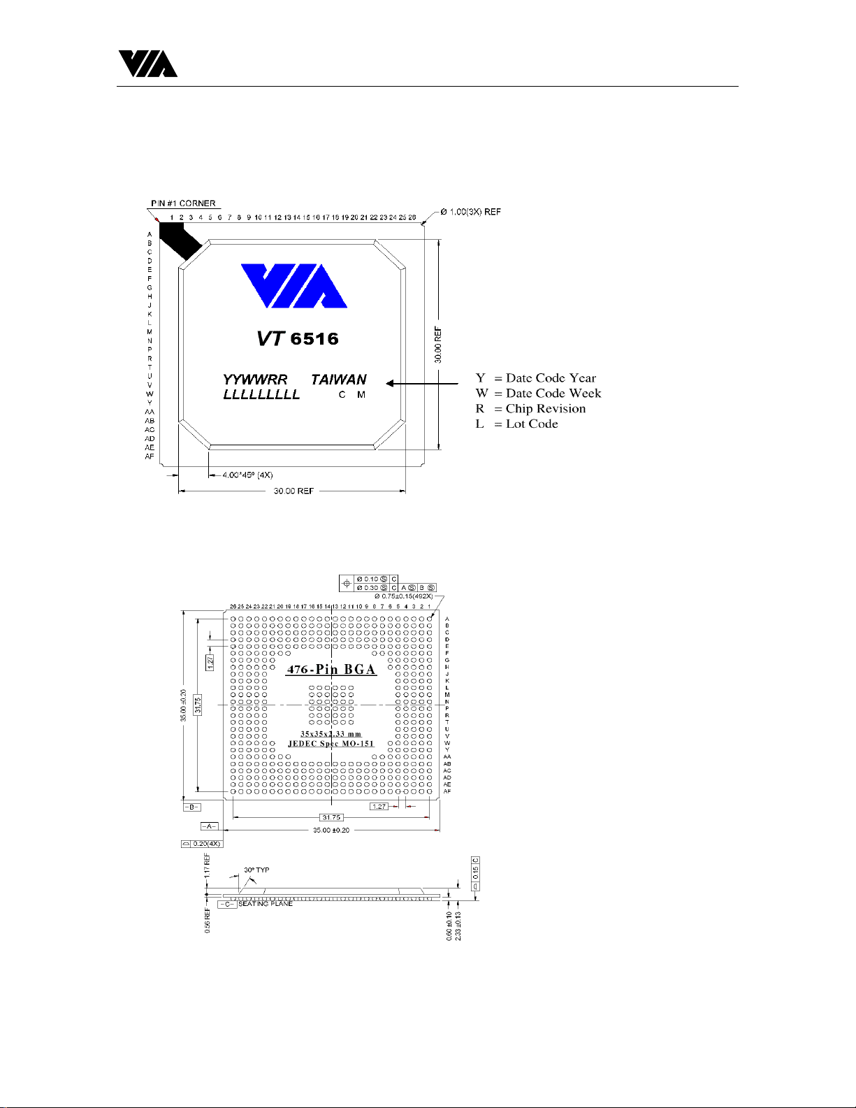
VIA Technologies, Inc. Preliminary VT6516 Datarsheet
PACKAGE MECHANICAL SPECIFICATIONS
-73-
 Loading...