

Page 1

VIA Technologies, Inc. Preliminary VT6304
VT6304
1394.A 4 PORT PHYSICAL LAYER CHIP
DATA SHEET
(Preliminary)
DATE : June 1, 1999
VIA TECHNOLOGIES, INC.
1
Page 2

VIA Technologies, Inc. Preliminary VT6304
PRELIMINARY RELEASE
Please contact Via Technologies for the latest documentation.
Copyright Notice:
Copyright © 1998, Via Technologies Incorporated. Printed in Taiwan. ALL RIGHTS RESERVED.
No part of this document may be reproduced, transmitted, transcribed, stored in a retrieval system, or
translated into any language, in any form or by any means, electronic, mechanical, magnetic, optical,
chemical, manual or otherwise without the prior written permission of Via Technologies Incorporated.
The VT6101/VT6102 may only be used to identify products of Via Technologies.
All trademarks are the properties of their respective owners.
Disclaimer Notice:
No license is granted, implied or otherwise, under any patent or patent rights of Via Technologies. Via
Technologies makes no warranties, implied or otherwise, in regard to this document and to the products
described in this document. The information provided by this document is believed to be accurate and
reliable to the publication date of this document. However, Via Technologies assumes no responsibility for
any errors in this document. Furthermore, Via Technologies assumes no responsibility for the use or misuse
of the information in this document and for any patent infringements that may arise from the use of this
document. The information and product specifications within this document are subject to change at any
time, without notice and without obligation to notify any person of such change.
Offices:
5020 Brandin Court 8th Floor, No. 533
Fremont, CA 94538 Chung-Cheng Rd., Hsin-Tien
USA Taipei, Taiwan ROC
Tel: (510) 683-3300 Tel: (886-2) 218-5452
Fax: (510) 683-3301 Fax: (886-2) 218-5453
Onlines Services:
BBS : 886-2-2186408
FTP : FTP.VIA.COM.TW
HTTP: WWW.VIA.COM.TW
2
Page 3

VIA Technologies, Inc. Preliminary VT6304
VT6304 IEEE 1394A FOUR PORT CABLE TRANSCEIVER/ARBITER FEATURES
n Supports Provisions of IEEE 1394-1995 Standard for High Performance Serial Bus and the P1394a
Supplement 2.0.
n Full P1394a Supplement Support includes:
n Arbitrated short reset,
n Connection Debounce,
n Multispeed Concatenation,
n Ack Accelerated Arbitration,
n Fly-By Concatenation,
n Programmable Port Disable, Suspend, Resume,
n PHY IDs Do Not Increment Past 63
n Provides Four 1394a Fully Compliant Cable Ports at 100/200/400 Megabits per Second (Mbit/s)
n Single 3.3 V power supply
n Logic Performs Bus Initialization and Arbitration Functions
n Encode and Decode Functions Included for Data-Strobe Bit-Level Encoding
n Incoming Data Resynchronized to Local Clock.
n Data Interface to Link-Layer Controller Provided Through 2/4/8 Parallel Lines at 49.152 MHz
n 24.576 MHZ Crystal Oscillator and PLL Provide TX/RX Data at 100/200/400 Mbps and Link-Layer
Controller Clock at 49.152 MHZ.
n Cable Power Presence Monitoring.
n Programable Node Power Class Information for System Power Management
n Embedded Bus Holder Isolation to Link Layer Controller Interface
n Optional On-chip Resistors to Reduce Component Counts for Electrical Isolation to Link Layer
Controller Interface
n Fully Compliant P1394a 2.0 PHY Map
n Separate TPBIAS for Each Port
n Fully Interoperable with IEEE Std1394-1995 Devices
n Cable Ports Monitor Line Conditions for Active Connection to Remote Node
n Low Power Design for Battery-Powered Applications includes: User Controlled Power-Down via PD,
Automatic Device Power-Down during All Ports Suspended and Link Interface Disabled, Link
Interface Power-Down via Inactive LPS, Automatic Inactive Ports Powered-Down, and Automatic
Inactive Logic Power-Down
n Self Power Up Reset and Pinless PLL to Reduce Component Counts on System
n Low Cost 100-Pin PQFP package
3
Page 4
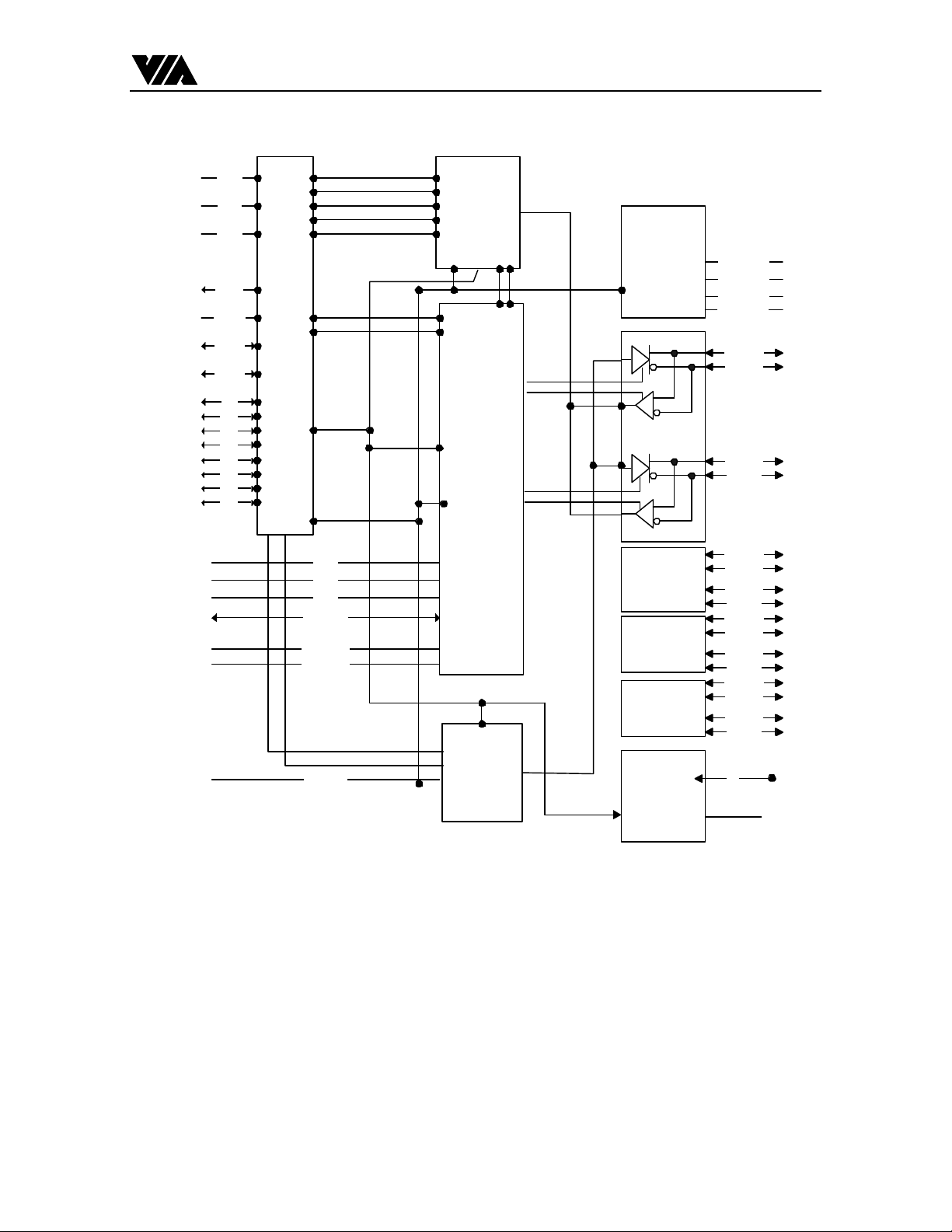
VIA Technologies, Inc. Preliminary VT6304
CPS
LPS
ISO\
SYS
CLK
LREQ
CTL0
CTL1
D0
D1
D2
D3
D4
D5
D6
D7
Link
Interfac
e I/O
PC0
PC1
PC2
C/LKON
TESTM1
TESTM2
Received
Data
Decoder/
Retimer
Arbitration
and Control
State
Machine
Logic
Bias Voltage
and Current
Generator
Cable Port 1
Cable Port 2
Cable Port 3
Cable Port 4
TPBIAS1
TPBIAS2
TPBIAS3
TPBIAS4
TPA1+
TPA1-
TPB1+
TPB1-
TPA2+
TPA2-
TPB2+
TPB2-
TPA3+
TPA3-
TPB3+
TPB3-
TPA4+
TPA4-
TPB4+
TPB4-
n
Transmit
RESET\
Data
Encoder
Figure 1: Functional Block of VT6304
4
Crystal
Oscillator,
PLL System,
and Clock
Generator
XI
XO
Page 5
VIA Technologies, Inc. Preliminary VT6304
GNDATX2
XTPBIAS1
VDDATX2
VDDARX2
XTPBIAS2
GNDATX3
XTPBIAS3
GNDARX2
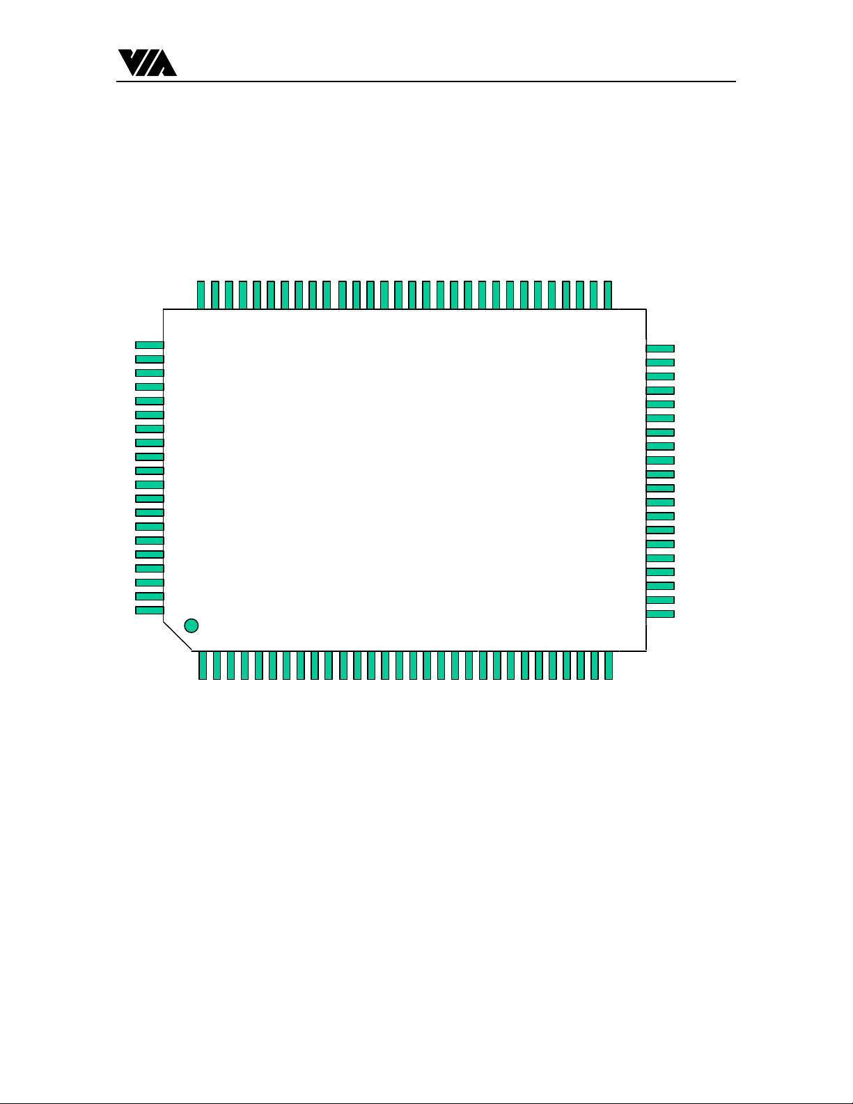
Pin Diagram
GNDD5
LINKON
LPS
CMC
VDDDC2
GNDDC2
XCPS
VDDARX0
GNDARX0
XTPB0M
XTPB0P
XTPA0M
XTPA0P
XTPBIAS0
VDDATX0
GNDATX0
GNDATX1
VDDATX1
VDDARX1
GNDARX1
NC
NC
NC
NC
NC
PD
ISO_
4
SCLK
VDDD
4
0
DDD
GNDD
3
1
VDDD
324
D
3
5
D
D
GNDD
2
1
CTL
VDDD
2
LREQ
GNDD
NC
0
6
7
D
CTL
D
80 79 78 77 76 75 74 73 72 7170 69 68 6766 65 64 63 62 6160 59 58 57 5655 54 53 52 51
81
82
83
84
85
86
87
88
89
VT6304
90
91
92
93
94
01/07/99 updated
95
96
97
98
99
100
1 2 3 4 5 6 7 8 9 10 11 12 13 14 15 16 1718 19 20 21 22 2324 25 26 27 28 29 30
NC
NC
NC
NC
50
49
48
47
46
45
44
43
42
41
40
39
38
37
36
35
34
33
32
31
CNA
RESET_
ONCT
TSI
GNDD1
VDDD1
PC0
PC1
PC2
TSO
VDDDC1
GNDDC1
XO
XI
XREXT
GNDAREXT
GNDARX3
VDDARX3
VDDATX3
GNDATX4
NC
NC
NC
NC
NC
XTPB1P
XTPB1M
XTPA1M
XTPA1P
XTPB2P
XTPB2M
XTPA2M
5
XTPA2P
XTPB3P
XTPB3M
XTPA3M
XTPA3P
NC
NCNCNC
NC
Page 6
VIA Technologies, Inc. Preliminary VT6304
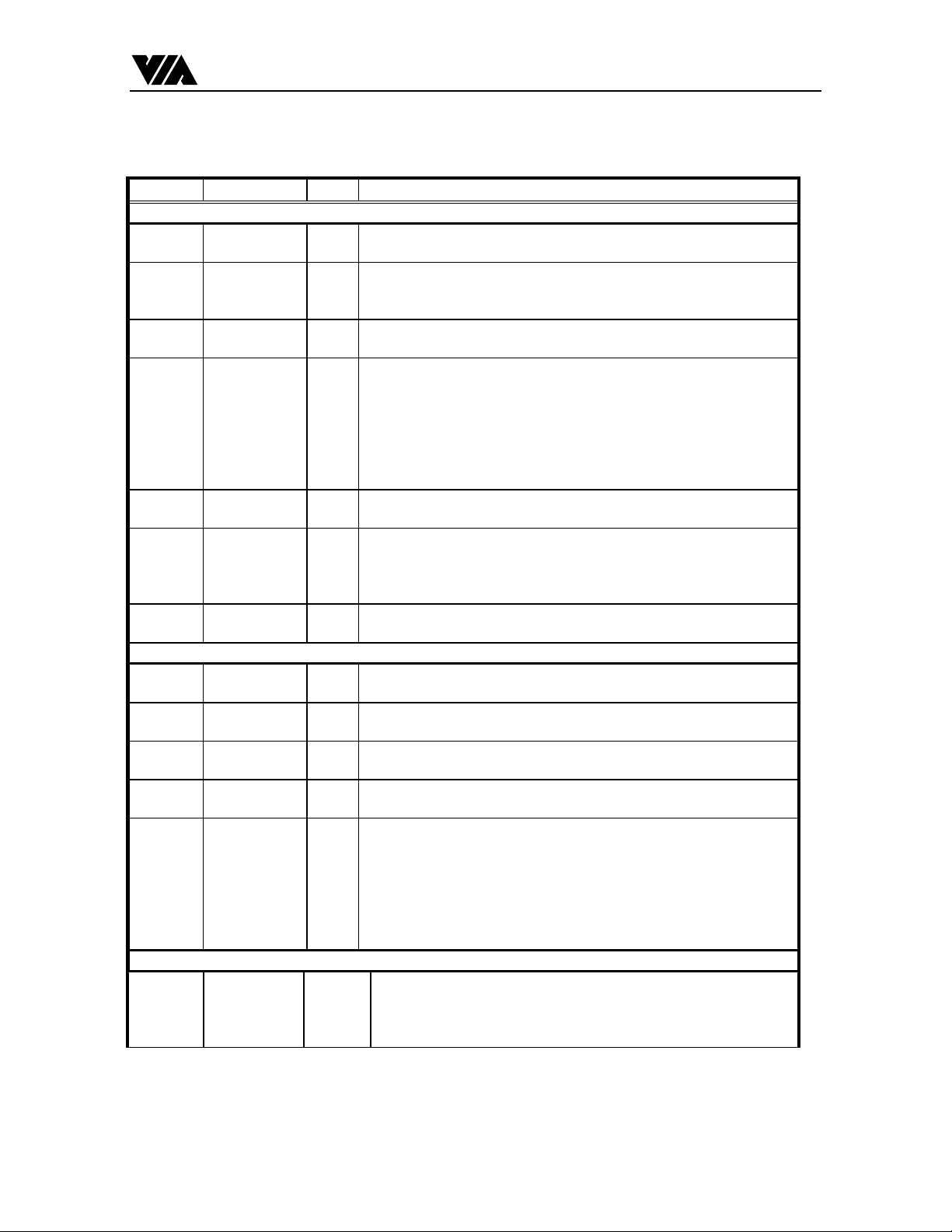
PIN DESCRIPTIONS
No. Name
Link-PHY Interface
82 LINKON O Link on. Indicates the reception of a link-on packet or port event
83 LPS I Link power status. LPS is connected to either the VDD supplying
57 LREQ I Link request. LREQ is an input from the LINK that requests the
74 ISO_ I Link interface isolation control input. This terminal controls the
60, 58 CTL[0-1] I/O Control I/O. the CTLn terminals are bidirectional
70, 69,
68, 66,
65, 64,
62, 61
72 SCLK O System clock. SCLK provides a 49.152 MHZ clock signal, which
Analog Interface
93, 10,
17, 22
92, 9 ,
16, 22
91, 8, 15,21XTPB[0-3]P I/O Twisted-pair cable B differential positive signal pins.
D[0-7] I/O Data I/O. The D terminals are bidirectional and pass data
XTPA[0-3]P I/O Twisted-pair cable A differential positive signal pins.
XTPA[0-3]M I/O Twisted-pair cable A differential negative signal pins.
Type
Description
occurs by asserting a 6.114 MHZ signal.
the LINK or to a pulsed output that is active when the LINK is
powered for the purpose of monitoring the LINK power status.
PHY to perform some service.
operation of output differentiation logic on the CTL[0-1] and
D[0-7] signals. If an optional isolation barrier is implemented
between the VT6304 and LLC the ISO_ pin should be tied low to
enable the differentiation logic. If no isolation barrier is
implemented, the ISO_ should be tied high to disable
differentiation logics.
communications control signals between the PHY and LINK.
between the PHY and LINK.
is synchronized with the data transfers to the LINK.
90, 7, 14,20XTPB[0-3]M I/O Twisted-pair cable B differential negative signal pins.
94, 11,
18, 23
Misc.
87 XCPS I CPS : Cable power status. CPS is normally connected to the
XTPBIAS[0-3]I/O Twisted-pair bias voltage supply. Provide 1.85V (typical) nominal
bias for proper operation of the twisted-pair cable drivers and
receivers, and for signaling to the remote nodes that the cable
connections is active. Hi-impedance during chip reset or power
down. Can be disabled via remote packets or software defined in
P1394a Draft 2.0. Each of these pin must be decoupled with a 1-uF
capacitor to ground.
cable power through a 11 Kohm/1 KOhm volatge divider. This
circuit drivers an internal comparator that detects the presencce
of cable power.
6
Page 7

VIA Technologies, Inc. Preliminary VT6304
50 CNA O CNA is asserted high when none of the PHY ports are
connected to another active port. This circuit remains active
during the powerdown mode.
84
44, 43, 42
47
41
48 ONCT I On Chip Termination. If the capacitive isolation barrier is
75 PD I Power Down. A logic High on this pin turns off all internal
49 RESET_ I/NC Reset (active low). The reset pin is connected to an internal 10K
38, 37 XI, XO Crystal Crystal Oscillator, 3.3V. These pins connect to a 24.576 MHz
36, 35 XREXT,
Power Supply & Ground
88, 99, 13,
33
89, 100, 25,
24
CMC I Programable Contender/Bus Manager Capable. It specifies in
the Self-ID packet that the node is capable of being a bus
manager.
PC[0-2] I Power Class. These pins are used to set the three
POWER_CLASS bits in the Self-ID packet. They are used to
describe the power consumption and source characteristics of
the node. PC0, 1, 2 are reflected in the Self-ID packet bits 21,
22, 23, respectively.
TSI I Single Self ID packet. If port 4 is unused, i.e, the resistors and
capacitors for port 4 are not implemented, there is no need to
send the 2nd self ID packet, and the system can get benefit by
tying this pin to digital VDD to reduce self ID packet exchange
time.
TSO I Test pin. Tied to VT6304 digital VDD ring for normal
operations.
implemented between the VT6304 and LLC, tie this pin to
VDD will utilize on chip resistors to replace on board 5K
Ohms resistors pair for LREQ, CTL[0:1] and D[0:7] at PHY
side. The resistors for LPS input at PHY side are also replaced
if this pin is tied to VDD. This pin has effects on on-chip
terminations only if ISO_ is tied to ground.
cicuitry except the connection detect circuits, which outputs
the CNA signal.
ohm resistor and an external 0.1 uF capacitor is used for
internal reset generation at power-on. The pin can be left
unconnected to save the external capacitors, and then the reset
time after power-on ranges from 0.5 ms to 2 ms. This pin can
also be driven by an open-drain type driver.
parallel resonant fundamental mode crystal. The optimum
values for the external shnut capacitors are dependent on the
specifications of the cystal used. The resulting frequency
variation is +/- 100 ppm.
I/O Current setting resistor terminals. A resistor of 6.2 KOhm +/-
GNDARE
0.5% is required for internal operating currents generation.
XT
VDDARX supply Analog receiver power. A combination of high-frequency
decoupling capacitors near these pins are suggested. These
pins are seperated from digital power for noise prevention.
GNDARX supply Analog receiver ground. These pins are tied together to the low-
impedance circuit board ground.
7
Page 8
VIA Technologies, Inc. Preliminary VT6304
95, 98, 12,
32
96, 97, 6,
19, 31
40, 85
39, 86
45, 59, 67,
73
46, 56, 63,
71, 81
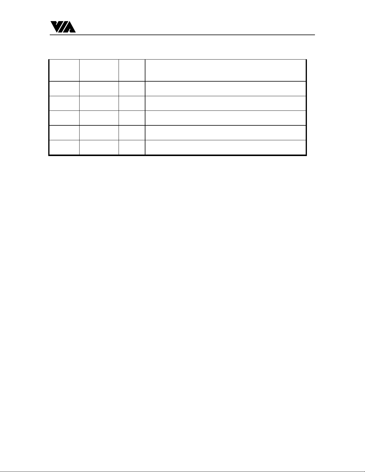
VDDATX supply Analog transmitter power. A combination of high-frequency
decoupling capacitors near these pins are suggested. These
pins are seperated from digital power for noise prevention.
GNDATX supply Analog transmitter ground. These pins are tied together to the
low-impedance circuit board ground.
VDDDC supply Digital core power. These pin are tied to low-impdance point on
the circuit board.
GNDDC supply Digital core ground. These pins are tied together to the low-
impedance circuit board ground.
VDDD supply Digital IO power. These pin are tied to low-impdance point on
the circuit board.
GNDD supply Digital IO ground. These pins are tied together to the low-
impedance circuit board ground.
8
Page 9

VIA Technologies, Inc. Preliminary VT6304
FUNCTIONAL DESCRIPTIONS
1. GENERAL DESCRIPTION
The VT6304 provides three-port physical layer function in a cable-based IEEE 1394-1995 network. Each
cable port incorporates two differential line transceivers. The transceivers include circuitry to monitor the
line conditions as needed for determining connection status, for initialization and arbitration, and for packet
reception and transmission.
Data bits to be transmitted through the cable ports are received from the Link on 2/4/8 data lines (D[0:7]),
and are latched internally in the VT6304 in synchronization with the 49.152-MHZ system clock. These bits
are combined serially, encoded, and transmitted at 98.304 , 196.608 or 393.216 Mbits/S as the outbound
data-strobe information stream. During transmission, the encoded data transmitted differential on the TPB
cable pair(s), and the encoded strobe information is transmitted differentially on the TPA cable pair(s).
During packet reception the TPA and TPB transmitters of the receiving cable port are disabled, and the
receivers for that port are enabled. The encoded data information is received on the TPA cable pair, and the
encoded Strobe information is received on the TPB cable pair. The received data-strobe information is
decoded to recover the receive clock signal and the serial data bits. The serial data bits are split into two or
four parallel transmitted (repeated) out of the other active (connected) cable ports.
Both the TPA and TPB cable interfaces incorporate differential comparators to monitor the line states during
initialization and arbitration. The output of these comparators are used by the internal logic to determine the
arbitration status. The TPA channel monitors the incoming cable common-mode voltage. The value of this
common mode voltage is used during arbitration to set the speed of the next packet transmission. In
addition, the TPB channel monitors the incoming cable common-mode voltage for the presence of the
remotely supplied twisted-pair bias voltage. The presence or absence of this common-mode voltage is used as
an indication of cable connection status. The cable connection status signal is internally debounced in the
VT6304 on a cable disconnect-to-connect. The debounced cable connection status signal initiates a bus reset.
On a cable disconnect-to-connect a debounce delay is incorporated. There is no delay on a cable disconnect.
2. NETWORK INTERFACE
9
Page 10
VIA Technologies, Inc. Preliminary VT6304
VT6304 REGISTERS
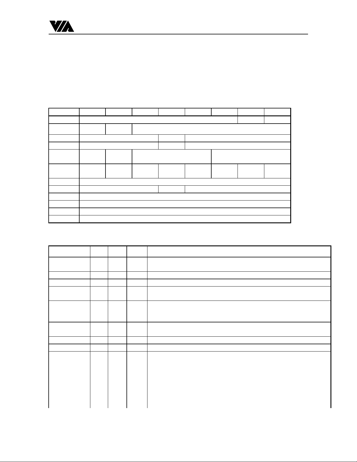
Definitions and usage for each of the registers listed below are provided on this and the following pages:
3. PHY REGISTER MAP FOR THE CABLE ENVIRONMENT
address 0 1 2 3 4 5 6 7
0000b Physical_ID R PS
0001b RHB
0010b Extended(7) reserved Total_ports
0011b Max_speed reserved Delay
0100b Link_activeContender Jitter Pwr_class
0101b Resume_intISBR Loop Pwr_fail Timeout Port_eventEnab_accelEnab_mul
0110b Reserved
0111b Page_select reserve Port_select
1000b Register0(page_select)
IBR
Gap_count
ti
1111b Register7(page_select)
3.1. PHY REGISTER FIELDS FOR THE CABLE ENVIRONMENT
size
Physical_ID 6 r - The address of this node determined during self-identification. A value of 63
R 1 r - When set to one, indicate that this node is the root.
PS 1 r - Cable Power status.
RHB 1 rw 0 Root hold-off bit. When set to one, instructs the PHY to attempt to become
IBR 1 rw 0 Initiate bus reset. When set to one, instructs the PHY to initiate a bus reset
Gap_count 6 rw 3F Used to configure the arbitration timer setting in order to optimize gap times
Extended 3 r 7 constant value of seven
Total_ports 5 r 3 the number of ports implemented by this PHY
Max_speed 3 r 010 Indicates the maximum speed this PHY supports;
type
default description
indicates a malconfigured bus; the link shall not transmit any packets.
the root during the next tree identify process.
immediately (without arbitration). This bit causes assertion of the reset state
for 166 us and is self-clearing.
according to the topology of the bus. IEEE 1394-1995 4.3.6
000 - 98.304 Mbit/s
001 - 98.304 and 196.608 Mbit/s
010 - ... and 393.216 Mbit/s
011 - ... and 786.43 Mbit/s
100 - nd 1,572.864 Mbit/s
101 - nd 3,145.728 Mbit/s
all other values are reserved for future definition
10
Page 11
VIA Technologies, Inc. Preliminary VT6304
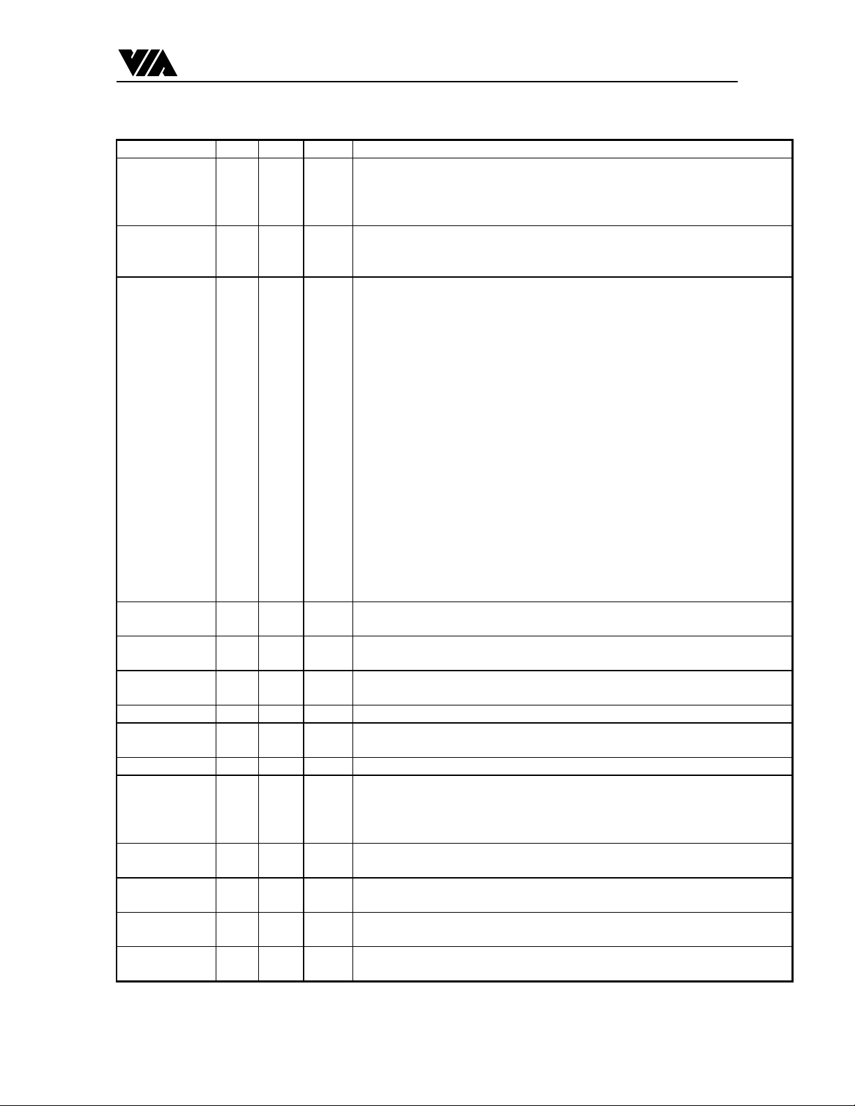
Delay 4 R 0 Worse case repeater delay, expressed as 144+(delay*20)ns.
Link_active 1 rw 1 Link enabled. Default value of one subsequent to a power reset. Otherwise
cleared or set by software to control the value of the L bit transmitted in the
self-ID packet. The transmitted L bit shall be the logical AND of this bit and
the LPS signal.
Contender 1 rw Pin
C/LKO
N
Pwr_class 3 rw Pin
PC0PC2
Contender. Cleared or set by software to control the value of the C bit
transmitted in the self-ID packet.
Power class. Controls the value of the pwr field transmitted in the self-ID
packet.
000 - Node does not need power and does not repeat power
001 - Node is self-powered and provides a minimum of 15 W to the
bus
010 - Node is self-powered and provides a minimum of 30 W to the
bus.
011 - Node is self-powered and provides a minimum of 45 W to the
bus
100 - Node may be powered from the bus and is using up to 1 W.
101 - Node is powered from the bus and is using up to 1 W. An
additional 2 W is needed to enable the link and higher layers.
110 - Node is powered form the bus and is using up to 1 W. An
additional 5 W is needed to enable the link and higher layers.
111 - Node is powered from the bus and is using up to 1 W. An
additional 9 W is needed to enable the link and higher layers.
Jitter 3 R 0 The difference between the fastest and slowest repeater data delay, expressed
as (jitter+1)*20ns
Resume_int 1 Rw 0 Resume interrupt enable. When set to one, the PHY shall set port_event to
one if resume operations commence for any port.
ISBR 1 rw 0 Initiate short (arbitrated) bus reset. A write of one to this bit instructs the
PHY to arbitrate and issue a short bus reset. This bit is self-clearing.
Loop 1 rw 0 Loop detect. A write of one to this bit clears it to zero.
Pwr_fail 1 rw 0 Cable power failure detect. Set to one when the PS bit changes from one to
zero. A write of one to this bit clears it to zero.
Timeout 1 rw 0 Arbitration state machine timeout. A write of one to this bit clears it to zero.
Port_event 1 rw 0 Port event detect. The PHY sets this bit to one if any of connected, Bias,
Disabled or Fault change for a port whose Int_enable bit is one. The PHY
also sets this bit to one if resume operations commence for any port and
Resume_int is one. A write of one to this bit clears it to zero.
Enab_accel 1 rw 0 Enable arbitration acceleration. When set to one, the PHY shall use the
enhancements specification in P1394A.
Enab_multi 1 rw 0 Enable multi-speed packet concatenation. When set to one, the Link shall
signal the speed of all packets to the PHY.
Page_select 3 rw 000 Selects which of eight possible PHY register pages are accessible through
the window at PHY register address 1000b through 1111b, inclusive.
Port_select 4 rw 0000 If the page selected by Page_select presents per port information, this field
selects which port’s registers are accessible through the window at PHY
11
Page 12
VIA Technologies, Inc. Preliminary VT6304
register addressed 1000b through 1111b, inclusive.
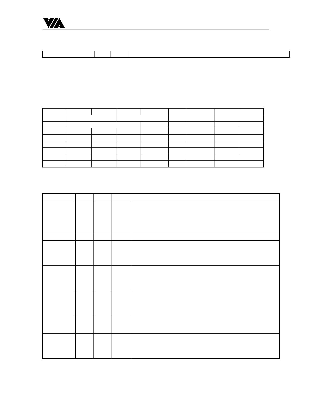
3.2. PHY REGISTER PAGE0: PORT STATUS PAGE
The port Status page is used to access configuration and status information for each of the
PHY’s port. The port is selected by writing zero to Page_select and the desired port number
to Port_select in the PHY register at address 0111.
0 1 2 3 4 5 6 7
1000b AStat BStat Child connected Bias Disabled
1001b Negotiated_speed Int_enable Fault
1010b
1011b
1100b
1101b
1110b
1111b
3.3. PHY REGISTER PORT STATUS PAGE FIELDS
Size Type default Description
Astat 2 r
Bstat 2 r - (same encoding as Astat)
Child 1 r - If equal to one, the port is a child, else a parent. The meaning of this
Conncted 1 r 0 If equal to one, the port is connected, else disconnected. The value
Bias 1 r - If equal to one, bias voltage is detected( possible connection). The
Disabled 1 rw 0 When set to one, the port shall be disabled. The value of this bit
Negotiated_sp
eed
3 r - Indicated the maximum speed negotiated between this PHY port and
- TPA line State for the port
00 = invalid
01 =1
10 =0
11 =z
bit is undefined from the time a bus reset is detected until the PHY
transitions to state T1:Child Handshake during the tree identify
process(see 4.4.2.2 in IEEE Std 1394-1995)
reported by this bit is filtered by hysteresis logic to reduce multiple
status changes caused by contact scrape when a connector is inserted
or removed.
value reported by this bit is filtered by hysteresis logic to reduce
multiple status changes caused by contact scrape when a connector is
inserted or removed.
subsequent to a power reset is implementation-dependent, but should
be a strappable option.
its immediately connected port; the encoding is
000 – 98.304Mbit/s
001 - and 196.608 Mbit/s
12
Page 13
VIA Technologies, Inc. Preliminary VT6304
010 - and 393.216 Mbit/s
Int_Enable 1 rw 0 Enable port event interrupts. When set to one, the PHY shall set
Port_event to one if any of Connected, Bias, Disabled or Fault (for this
port) change state.
Fault 1 Rw 0 Set to one if an error is detected during a suspend or resume operation.
A write of one to this bit clears it to zero.
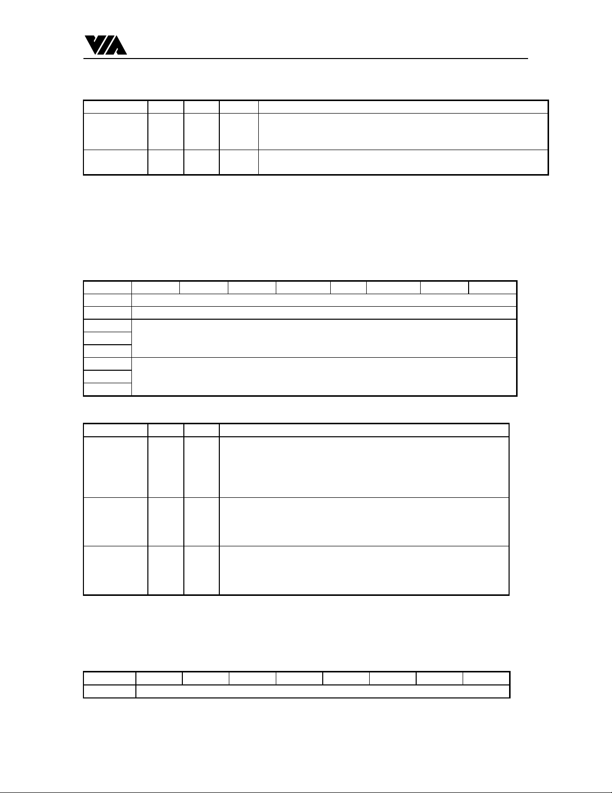
3.4. PHY REGISTER PAGE 1: VENDOR IDENTIFICATION PAGE
The Vendor Identification page is used to identify the PHY’s vendor and compliance level. The page is
selected by writing one to Page_select in the PHY register at address 0111.
0 1 2 3 4 5 6 7
1000b Compliance_level
1001b Reserved
1010b
1011b
1100b
1101b
1110b
1111b
Vendor_ID
Product_ID
3.5. PHY REGISTER VENDOR IDENTIFICATION PAGE FIELDS
Size Type Description
Compliance_le
vel
Vendor_ID 24 R The company ID or Organizationally Unique Identifier (OUI) of the
Product_ID 24 R The meaning of this number is determined by the company or
8 R Standard to which the PHY implementation complies:
0 = not specified
1 = IEEE P1394a
All other values reserved for future standardization. The default is
“1”.
manufacturer of the PHY. The most significant byte of Vendor_ID
appears at PHY register location 1010 and the least significant at
1100. The default value is “00 40 63”.
organization that has been granted Vendor_ID. The most significant
byte of Product_ID appears at PHY register location 1101 and the
least significant at 1111. The default value is “30 60 00”.
3.6. PHY REGISTER PAGE 7: VENDOR-DEPENDENT PAGE
The vendor-dependent page provides registers set aside for use by the PHY’s vendor. The page is selected by
writing seven to Page_select in the PHY register at address 0111. Don’t access the registers “used for
test”.
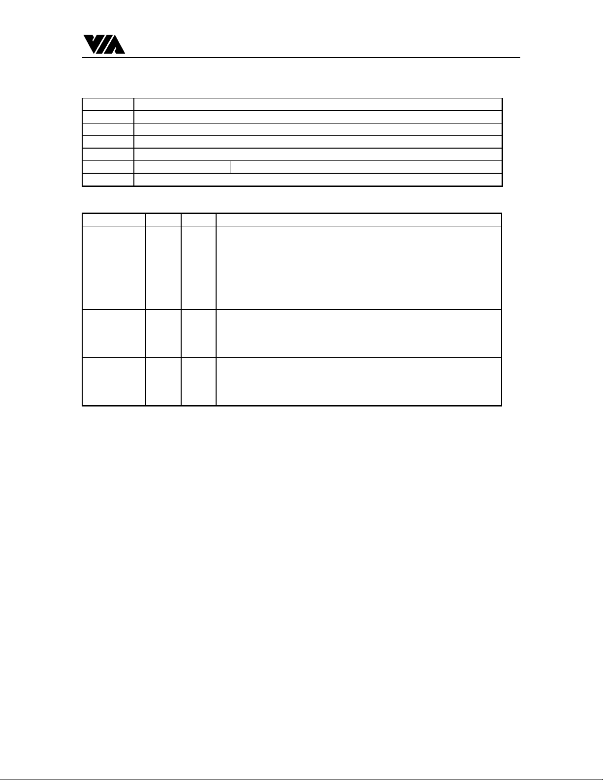
address 0 1 2 3 4 5 6 7
1000b used for test
13
Page 14
VIA Technologies, Inc. Preliminary VT6304
1001b used for test
1010b used for test
1011b used for test
1100b used for test
1101b used for test
1110b Link_Speed Reserved
1111b used for test
3.7. PHY REGISTER VENDOR DEPENDENT PAGE FIELDS
Size Type Description
Link_Speed 2 RW Link speed. This field indicates the top speed capability of the
attached LLC. Encoding is as follows :
This field has the effect on the self-ID packets as well as the PHY
speed capability which is exchanged between peer PHY during self-ID
state. This field is set to 10b (S400) by hardware reset and is
unchanged by bus-reset.
Vendor_ID 24 R The company ID or Organizationally Unique Identifier (OUI) of the
manufacturer of the PHY. The most significant byte of Vendor_ID
appears at PHY register location 1010 and the least significant at
1100. The default value is “00 e0 4c”.
Product_ID 24 R The meaning of this number is determined by the company or
organization that has been granted Vendor_ID. The most significant
byte of Product_ID appears at PHY register location 1101 and the
least significant at 1111. The default value is “88 01 00”.
14
Page 15
VIA Technologies, Inc. Preliminary VT6304
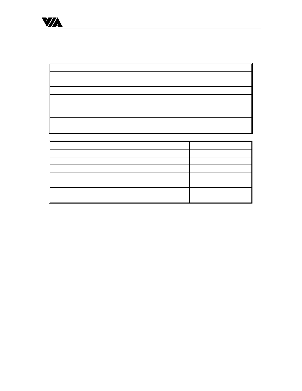
4 ELECTRICAL CHARACTERISTICS
4.1 ABSOLUTE MAXIMUM RATINGS
Supply Voltage (OVDD) -0.3 V to +3.6 V
Supply Voltage (OVDD_AUX) -0.3 V to +3.6 V
DC Output Voltage (VOUT) -0.3 V to VDD+0.3V
Storage Temperature Range (T
STG)
Ambient Temperature (TA)
Lead Temp. (TL) (Soldering, 10 sec)
ESD Rating (R
ZAP = 1.5k, CZAP = 120 pF)
Input Latchup Current +/- 25mA
Package Power Dissipation 3.0Watt@250C
4.2 RECOMMENDED OPERATING CONDITIONS
Supply voltage V
Supply voltage V
Supply Current (IDD) D0 State
Supply Current (I
Supply Current (I
Supply Current (I
Supply Current (IDD) Low Power Mode
Supply Current (I
DD
DD
) D0 State
DD_AUX
) D3cold and PME Enable State
DD_AUX
) D3cold and PME Disable State
DD_AUX
) Low Power Mode
DD_AUX
-40°C to 125°C
0 to 70°C
250°C
2.0 KV
3.3 Volts ± 5%
3.3 Volts ± 5%
15
Page 16
VIA Technologies, Inc. Preliminary VT6304
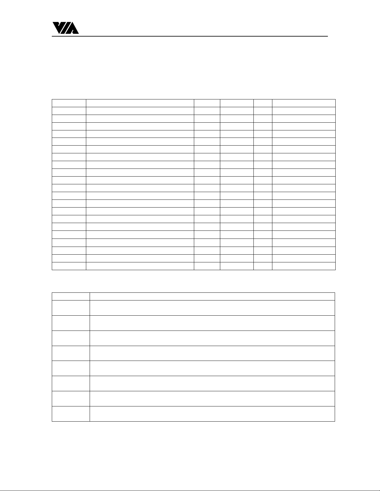
5.3 DC Electrical characteristics
4.3.1 Link PHY Interface DC Specification
Unless otherwise noted, all test conditions ate as follows:
Table 1. DC Characteristics
Functional Operating Range (V
Symbol Parameter Min Max Unit Notes
V
V
V
V
V
V
V
V
V
V
V
V
I
I
I
I
I
I
C
C
C
IL1
IH1
IL2
IH2
IL3
IH3
IL4
IH4
OL1
OH1
OL2
OH2
OL1
OH1
OL2
OH2
LI1
LI2
IN
OUT
I/O
Input Low Voltage 0.9 V 1
Input High Voltage 2.4 V 1
Input Low Voltage 1.1 V 1
Input High Voltage 2.2 V 1
Input Low Voltage 1.1 V 1
Input High Voltage 2.2 V 1
Input Low Voltage 0.9 V 1
Input High Voltage 2.1 V 1
Output Low Voltage 0.1Vcc V 1
Output High Voltage 0.9Vcc V 1
Output Low Voltage 0.1Vcc V 1
Output High Voltage 0.9Vcc V 1
Output Low Current 9.0 18.7 mA 1, @ V
Output High Current 8.2 16.2 mA 1, @ V
Output Low Current 8.5 17.8 mA 1, @ V
Output High Current 7.7 15.4 mA 1, @ V
Input Leakage Current 50
Hi-Z State Data Line Leakage 50
Input Capacitance 12 pF FC = 1MHz
Output Capacitance 12 pF FC = 1MHz
I/O Capacitance 12 pF FC = 1MHz
NOTES:
1. Refer to table 2 for the signals associated with this specification.
Table 2. DC Characteristic Signal Association (Sheet 1 of 2)
Symbol Associated Signals
V
IL1
/ V
**** Input Type 1 (1394) ****
IH1
CNA, CTL[0:1], D[0:7], LINKON, LREQ, SCLK
V
IL2
/ V
**** Input Type 2 ****
IH2
CMC, ISO_, ONCT, PC[0:2], TSI, TSO
V
IL3
/ V
**** Input Type 3 ****
IH3
LPS, PD
V
IL4
/ V
**** Input Type 4 ****
IH4
RESET_
V
OL1
/ V
**** Output Type 1 ****
OH1
CNA, CTL[0:1], D[0:7], LINKON, LREQ, SCLK
V
OL2
/ V
**** Output Type 2 ****
OH2
CMC, ISO_, ONCT, PC[0:2], TSI, TSO
I
OL1
/ I
**** Output Type 1 ****
OH1
CNA, CTL[0:1], D[0:7], LINKON, LREQ, SCLK
I
OL2
/ I
**** Output Type 2 ****
OH2
CMC, ISO_, ONCT, PC[0:2], TSI, TSO
= 5V±5%, VCC = 3.3V±0.3V, T
REF
= 0 to +85)
CASE
A
A
OL1
OH1
OL2
OH2
(0V < VIN < 3.3 V)
Table 3. DC Current Characteristic
16
Page 17
VIA Technologies, Inc. Preliminary VT6304
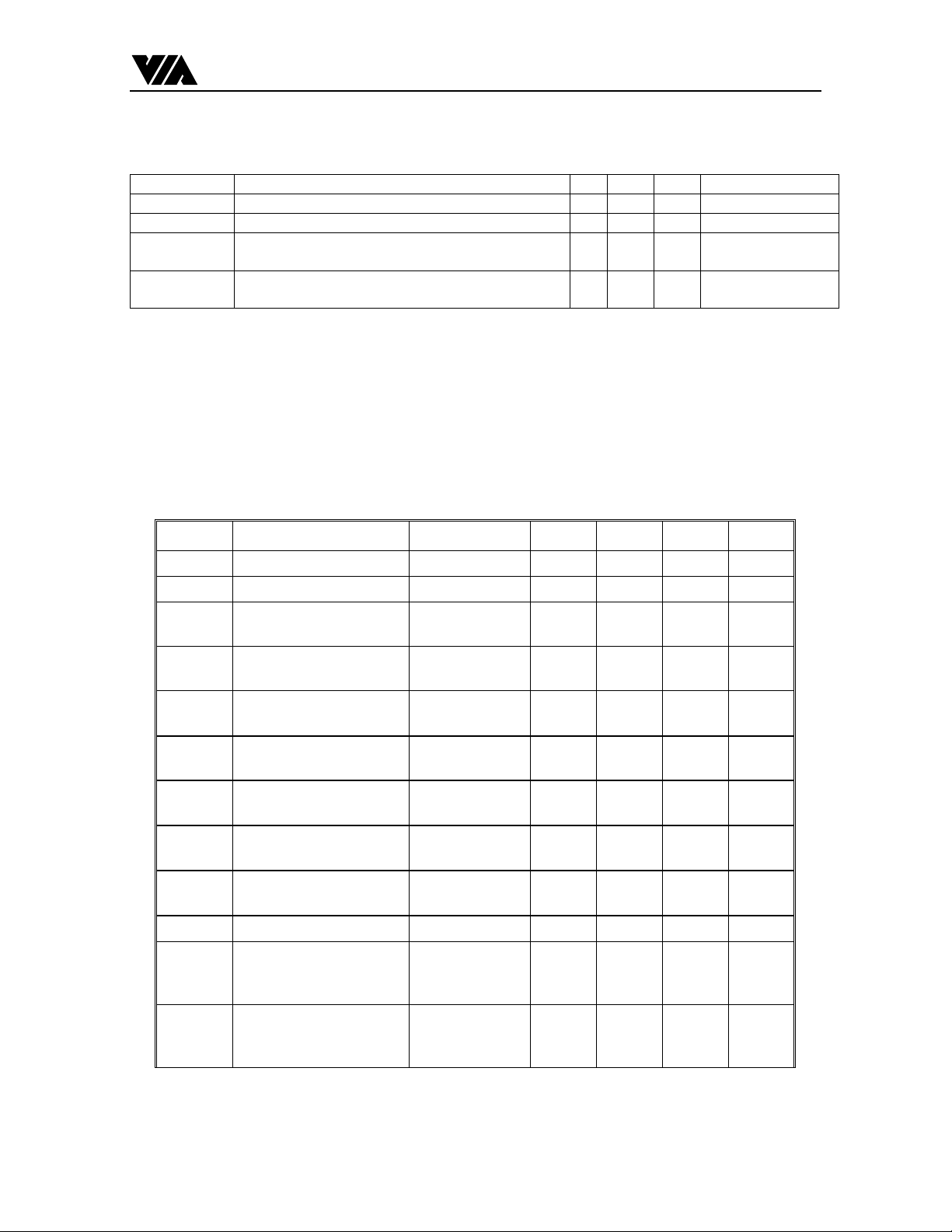
Functional Operating Range (V
= 5V±5%, VCC = 3.3V±0.3V, T
REF
= 0 to +85)
CASE
Symbol Parameter Typ Max Unit Notes
ICC(3v) VCC Supply Current 110 155 mA
ICC(SUS) ON Suspend Well Supply Current – Full On 3 5 mA
ICC(SUS)
POS/STR
ICC(SUS)
STD/Soff
Suspend Well Supply Current – Power On
Suspend or Suspend to RAM
Suspend Well Supply Current – Suspend to Disk or
Soft Off
30 150
9 150
A
A
4.3.3 Analog Signals DC Specification
Unless otherwise noted, all test conditions ate as follows:
1. TA = 0 to +700C
2. VCC = 3.3V +/- 10%
3. 24.576 Mhz +/- 0.01%
4. REXT = 6.2 K +/- 1%, no load
SYMBOL PARAMETER CONDITION MIN TYP MAX UNIT
V
V
I
IL
Input Low Voltage OSCIN 1.5 Volt
IL
Input High Voltage OSCIN 3.5 Volt
IH
Input Low Current VIN=GND.
-150
OSCIN
I
IH
Input High Current VIN=VCC.
150
OSCIN
V
Output Low Voltage IOL= -4 mA
OL
0.4 Volt
TPO±
IOL= -20 mA,
1 Volt
PLED[3:0]#
V
OH
Output High Voltage IOH= 4 mA
VCC-1.0 Volt
TPO±
IOH= 4 µA
VCC-1.0 Volt
PLED[3:2]#
IOH= 6 µA
2.4 Volt
PLED[1:0]#
C
I
CC
Input Capacitance 5 pF
IN
VCC Supply Current Transmitting,
170 mA
100Mbps, 4
portss
Transmitting,
220 mA
200Mbps, 4
ports
µA
µA
17
Page 18

VIA Technologies, Inc. Preliminary VT6304
Transmitting,
400 Mbps, 4
ports
Powerdown
Mode
280 mA
0.1 mA
18
Page 19
VIA Technologies, Inc. Preliminary VT6304
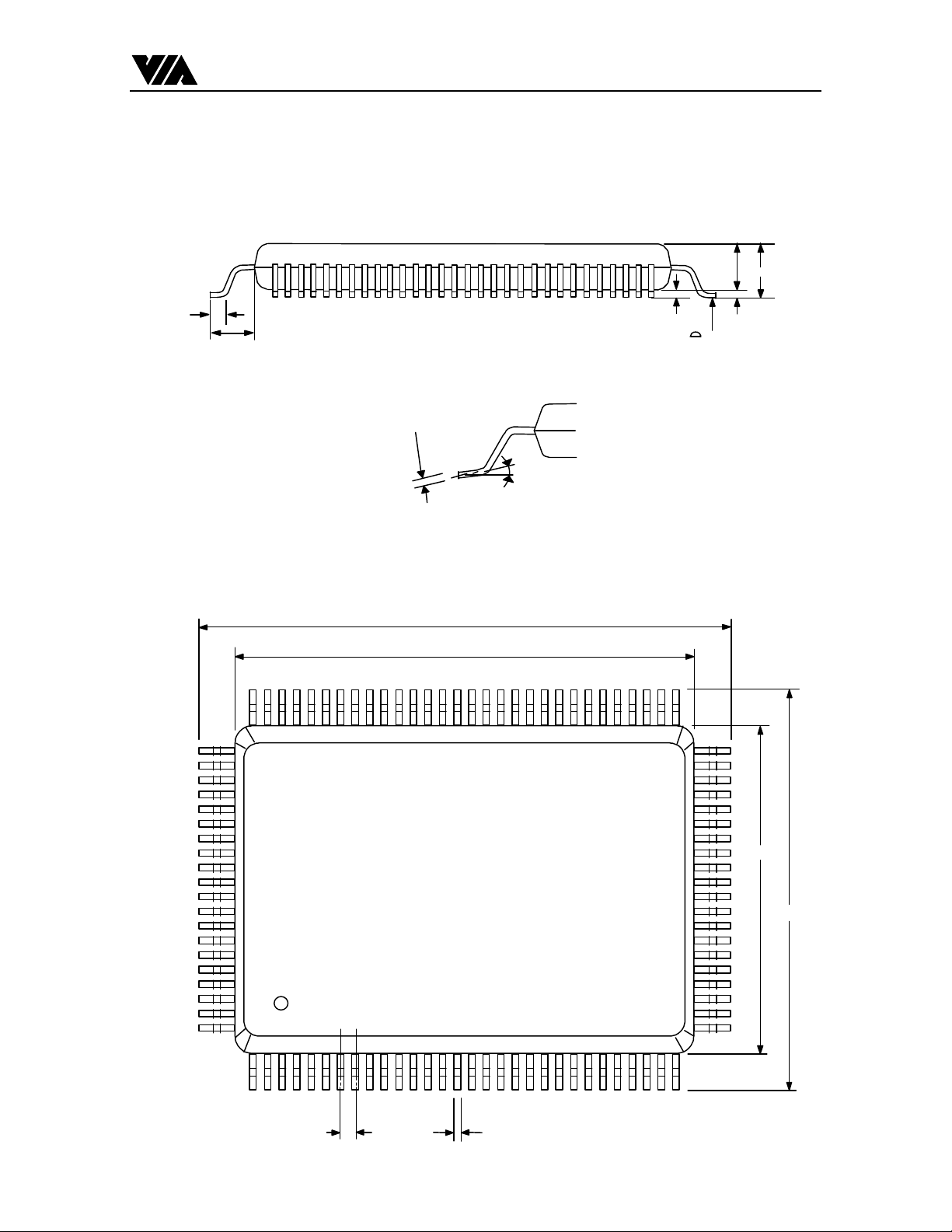
Package Diminsion
Unit Millimeter/Inch
0.88/.035
1.6/.063
Unit Millimeter/Inch
0.15+0.102 /
0.15-0.051
23.2/.913
20.0/0.787
0~7
2.72/.107
0.25/.01MIN
o
5180
3.40MAX
0.15MAX
100
81
1
0.2+0.030 / 0.008+0.001
0.5/.020
30
50
14.0/.551
17.2/.677
31
19
Page 20

VIA Technologies, Inc. Preliminary VT6304
[This page left to blank]
20
Page 21

VIA Technologies, Inc. Preliminary VT6101/VT6102
21
 Loading...