

Page 1
Preliminar
y
V
C
O
T73127
27 MHz 3.3V VCXO with Output Enable
Applications
•= Crystal-driven clock source
General Description
The Vaishali VT 73127 is a single-chip, low-jitter Voltage-Controlled-Cr ystal-Oscillator. The device accepts
a 27 MHz, 20 pF crystal input, and produces a low jitter output at the same frequency. The output is
enabled when OE is logic HIGH and goes into high impedanc e state when OE is logic LOW . A 0 to 3.0V
control signal is used to fine tune the output clock frequency in the ±100ppm range.
Features
•= 3.3V operating voltage
•= Uses inexpensive pullable crystals
•= 12mA drive capability at TTL levels
•= On-chip oscillator with 200 ppm pull range (±100 ppm)
•= Active High output enable
•= Die only
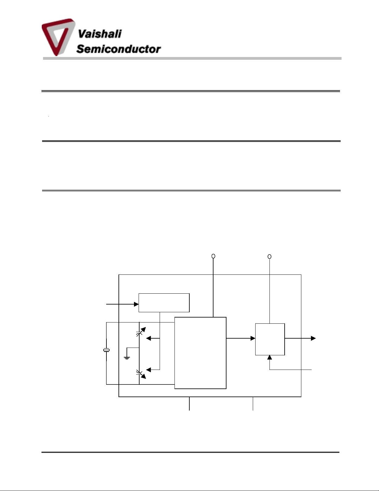
Figure 1. Functional Block Diagram
2001-08-06 Page 1 MDST-0012-02
27 MHz
Pullable
Crystal
Vaishali Semic onductor 747 Camden Avenue, Suite C Cam pbel l CA 95008 Ph. 408.377.6060 Fax 408.377.6063
VIN
X2
X1
Load Cap Control
Load
Caps
www.vaishali.com
VDD1
Oscillator
GND
VDD2
GND
Output
Buffer
LK
E
Page 2
VT73127 Preliminary
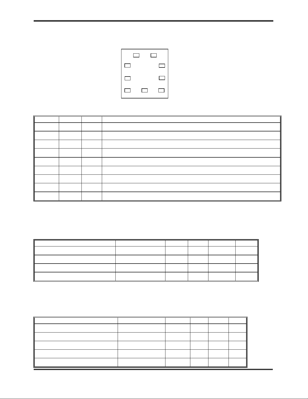
Figure 2. Pad Configuration
VDD1
VIN
GND
VT73127/D
X1
1
2
3
4
X2
9
8
GND
7
VDD2
5
OE
6
Table 1. Pad Description
Name Pad Type Description
X1 1 Xi Crystal connection. Connect to a 27 MHz pullable crystal
VDD1 2 P Core VDD. Connect to 3.3V
VIN 3 I Tuning control input. Zero to 3.3V signal controls the frequency of the VCXO.
GND 4 P Connect to ground.
CLK 5 O Clock output
OE 6 I Active HIGH output enable. When LOW, the output is held in a tri-state condition
VDD2 7 P Output buffer V
GND 8 P Connect to ground.
. Connect to 3.3V
DD
X2 9 Xi Crystal connection. Connect to a 27 MHz pullable crystal.
Legend: I = Input
O = Output
P = Power supply connection
Xi = Crystal connections.
Table 2. Absolute Maximum Ratings
Parameter Conditions Min Typ Max Units
Supply voltage, VDD Referenced to GND 7 V
Inputs and Clock Outputs Referenced to GND -0.5 VDD+0.5 V
Soldering Temperature Max of 10 seconds 260 °C
Storage temperature -65 150 °C
Stresses above those listed under Absolute Maximum Ratings may cause permanent damage to the device. These
ratings are stress specifications only and correct functional operation of the device at these or any other conditions
above those listed in the operational sections of the specifications is not implied. Exposure to absolute maximum rating
conditions for extended periods may affect product reliability.
Table 3. Operating Conditions
Parameter Conditions Min Typ Max Units
Operating Voltage, VDD 3.0 3.3 3.6 V
Input High Voltage, VIH, X1 pin only 2.5 V
Input Low Voltage, VIL, X1 pin only 0.4 V
Operating Temperature 0 70 °C
Input crystal accuracy ±30 ppm
2001-08-06 Page 2 MDST-0012-02
www.vaishali.com
Vaishali Semic onductor 747 Camden Avenue, Suite C Cam pbel l CA 95008 Ph. 408.377.6060 Fax 408.377.6063
Page 3

VT73127 Preliminary
VCXO control voltage, VIN 0 3.3 V
2001-08-06 Page 3 MDST-0012-02
www.vaishali.com
Vaishali Semic onductor 747 Camden Avenue, Suite C Cam pbel l CA 95008 Ph. 408.377.6060 Fax 408.377.6063
Page 4
VT73127 Preliminary
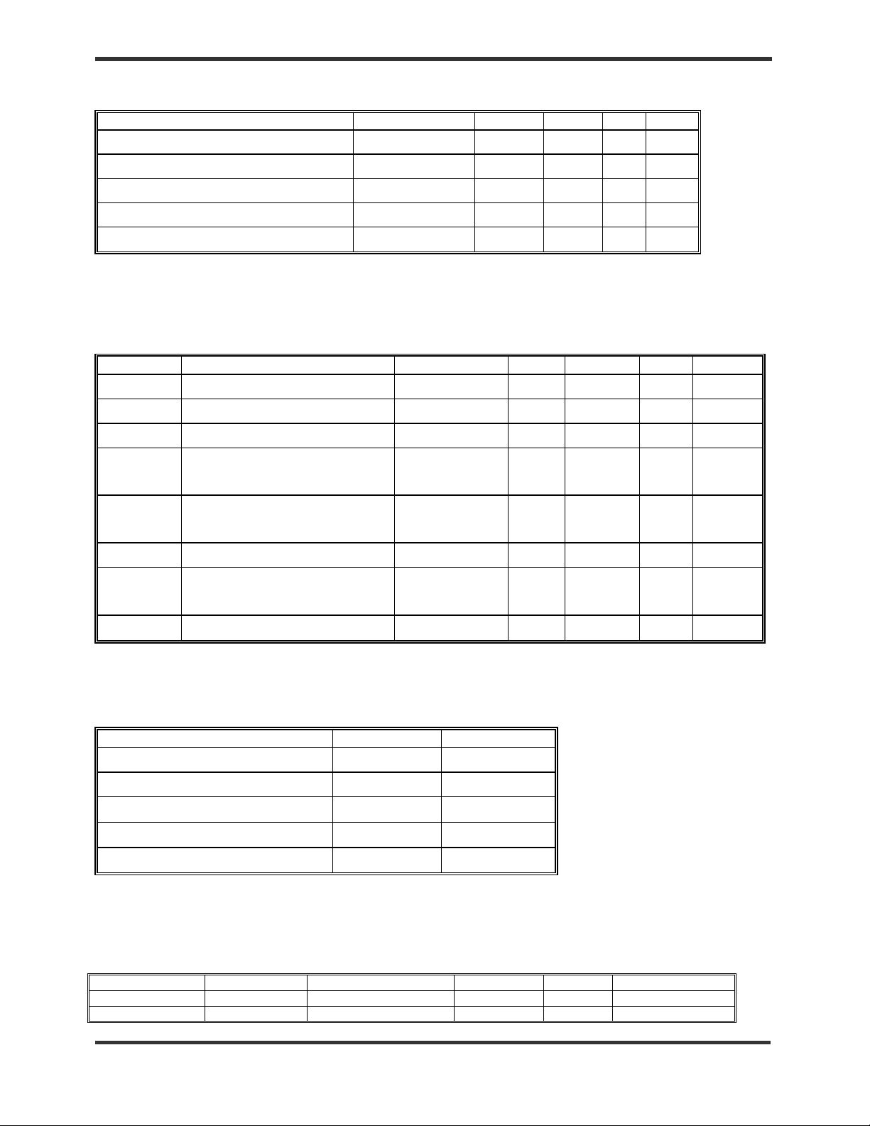
Table 4. DC Electrical Characteristics
TA = 0°C to +70°C, VDD = 3.0 V to 3.6 V
Parameter Condition Min Typ
Output High Voltage, VOH I
Output Low Voltage, VOL I
=-12mA 2.4 V
OH
=12mA 0.4 V
OL
(1)
Max Units
Operating Supply Current, IDD No Load 25 mA
Short Circuit Current Each output ±85 mA
Input Capacitance 7 pF
Note:
1. Typical values are at V
= 3.3V and 25°C
DD
Table 5. AC Electrical Characteristics
TA = 0°C to +70°C, VDD = 3.0 V to 3.6 V
Symbol Parameter Condition Min Typ Max Units
fosc Input Crystal Frequency 27 MHz
tr Output Clock Rise Time 0.8 to 2.0V 1.5 ns
tf Output Clock Fall Time 2.0 to 0.8V 1.5 ns
t
PZL
t
PZH
t
PLZ
t
PHZ
tod Output Clock Duty Cycle At VDD/2 40 60 %
Output Enable Time
(OE to CLK)
Output Disable Time
(OE to CLK)
6.5 ns
6.5 ns
t
(pk – pk) Maximum Absolute Jitter
jit
150 ps
(Peak to Peak)
Output pullability
Note:
1. Typical values are at V
= 3.3V and 25°C
DD
0V ≤V
≤ 3.3V
IN
±100 ppm
Table 6 Pullable Crystal Specifications
Parameter Symbol Value
Correlation (Load) Capacitance CL 20pF
Capacitance Ratio CO/C1 240 max
ESR
Initial Accuracy
Temperature and Aging Stability
50 Ω max
±30ppm
±50ppm
Ordering Information
VT73127
Part Number Marking Shipping/Packaging No. of Pads Package Temperature
VT73127/D Dice in waffle-pack 0oC to +70oC
VT73127/DW Dice in wafer form 0oC to +70oC
2001-08-06 Page 4 MDST-0012-02
www.vaishali.com
Vaishali Semic onductor 747 Camden Avenue, Suite C Cam pbel l CA 95008 Ph. 408.377.6060 Fax 408.377.6063
 Loading...