

Page 1
VT5F9MN0006/07
RF Data Sheet
FEATURES
• Stabilized, compact, and lightweight design.
• A board-in type mountable directly on the mother
board of the set.
• Bus noise elimination th rough the use of a built-in
white clip ci r cuit.
• Usable for many purposes such as BS, CATV , etc.,
in addition to VCR and laser disc.
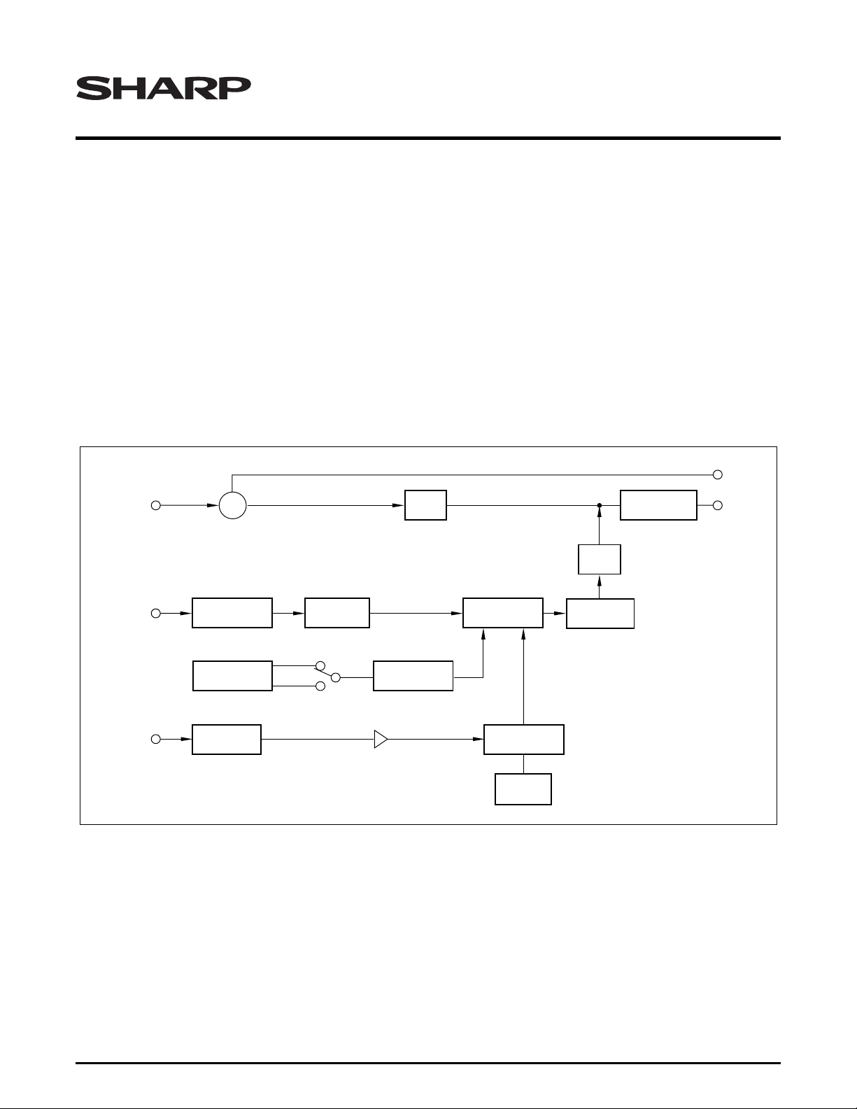
FUNCTIONAL DESCRIPTION
This modulator is designed for operation in NTSC-M
systems. An RF antenna input is provided by an F
Female connector and the combined RF output is provided on an F connector. The antenna input signals
ANTENNA
IN
DISTRIBUTOR
RF Modulator
appear on the RF output when the modulator portion is
not operatin g, allowing for transp arent operati on with
other household video ap pliances. When the m odulator is in use, the modulated signal is seen at output and
the antenna input spectrum is suppressed.
A tuner-out port is included in the VT5F9MN0007 as
this unit is intended for applications where a local tuner
capability is desired, such as in a combine VCR product. The tuner-out port is a sample of the antenna input
spectrum and is always active. The modulator may also
be used in satellite television applications. The out put
channel may be selected be tween NTSC c hannels 3
and 4, as designated in North America. The modulator
operates from a +5 V source.
RF SW
HIGH
PASS FILTER
TUNER
OUT
TV
OUT
VIDEO
IN
AUDIO
IN
VIDEO
CLAMPER
SAW
RESONATOR
PRE-
EMPHASIS
WHITE
CLIPPER
RF CARRIER
OSC
CH SW
AMP
Figure 1. Block Dia gr a m
MODULATOR
FM
MODULATOR
TANK
(4.5 MHz)
RF SW
BANDPASS
FILTER
MOD20-3
RF Data Sheet 1
Page 2

VT5F9MN0006/07 RF Modulator
SPECIFICATIONS
General Description
• U.S. standard transmission system
• NTCS color system
• Output channel 3, 4
• Output impedance 75 Ω, unbalanc ed
• Power source 5 (VDC) +B (MOD)
Test Condition
• Power source 5 ±0.1 (VDC) +B (MOD)
– Ripple 30 mVp-p MAX.
• Unit setting conditions
– Video: Apply 75% modulated color bar signal 1
Vp-p and set modulation factor and V/S ratio to
specified values. For modulation factor setting,
WHITE signal shall be 1 Vp-p V/S = 7/3,
APL = 50%.
– Audio: Add 1.24 Vp-p
• Ambient Conditions
– Temperature 25°C ±3
– Humidity 65% ±5 RH
– If judgment is not in doubt, standard tem pera-
ture may be considered as 15° to 30°C and humidity 45% to 85% RH.
Electrical Performance (RF MOD Portion)
• Video Characteristics
– Input impedance 1 kΩ ±30%, unbalanced
– Measure at 0 to 4.2 MHz
– Input signal level 1 Vp-p synchronous (–)
– When load of 82 Ω is applied
– Modulation factor 77 ±7%
– When load of 82 Ω is applied
– V/S Ratio
– 7 +0.25, -0. Input: Staircase wave 1 Vp-p syn-
chronous (–)
– 3 +0, -0.25. V/S = 7/3
– Amplitude frequency characteristics +2 dB, -3
(MAX.)
– Using 1 MHz as a standard in the 0 to 4.2 MHz
range, measure at RF output using multibu rst
or sweep generator. Spectrum analyze r band
is 300 kHz.
– Differential gain 10% (MAX.)
– Superimposed 3.58 MHz sine wave level shall
be 20% of sta irc as e w av e lev el, m eas ur ed in a
modulation factor range of 65% to 75% and an
APL ran ge o f 10 % to 90%. Ho weve r, d i ffe rent i al
gain of demo dulator unit shall req uire correc tion.
– Differential phase 10° (MAX.)
– Superimposed 3.58 MHz sine wave level shall
be 20% of staircase wave level, measured in a
modulation factor range of 65% to 75% and an
APL rang e o f 10 % to 90%. Howev e r, d if fer enti al
gain of demo dulator un it shall requ ire corr ection.
– Change in modulation factor to APL ±5% (MAX.)
– Within an APL range of 10% to 90% with APL
50% as referenced.
– S/N ratio 45 dB (p-p/rms MIN.)
– Measure with standard demodulator output.
• Audio system characteristics
– Input impedance 30 kΩ, unbalanced (MIN.)
– Measure at 0.1 to 10 kHz
– Input signal level 1.24 Vp-p
– Amplitude frequency characteristics +2 dB, -3 dB
– Using 1 kHz as a standard in the 100 Hz to
10 kHz range, measure deviation between reference.
– Modulation factor 90 ±20%
– 100% = ±25 kHz (±25 kHz ±5 kHz)
– Distortion rate 3% (MAX.)
– S/N ratio 45 dB (MIN.), includes buzz
• Output system characteristics.
– Video carrier frequency ±100 kHz (MAX.)
– For test conditions, temperature shall be 25°C,
and humidity 65% RH.
– Audio frequency 4,500 kHz ±7 (MAX.)
– For test conditions, temperature shall be 25°C,
and humidity 65% RH.
– Video output level 66 dBµ ±3 (MAX.)
– p-p level (AT modulation): 75 Ω load
– Audio output level difference (P/S ratio) 16 dB +4,
-3 (MAX.)
– Difference between video output lev el and au-
dio output level (audio non-modulation)
– Output terminal spurious
– Specific frequency 16 dB +4, -3 (MAX.)
fp–4.5MHz
– Other frequencies 30 dB (MIN.). Measure as
per FCC regulations: 0 to 1,000 MHz, excluding frequency in preceding remark.
– Spurious radiation within the band 60 dB (MIN.)
– Between fp and fs
– Chroma beat (920 kHz) 50 dB (MIN.)
– Apply 3.58 MHz 0.3 Vp-p sine wave to video in-
put and measure using spectrum analyzer.
– Output VSWR 3 (MAX.)
– Worst point in the band at 75 Ω termination.
2 RF Data Sheet
Page 3

Discription VT5F9MN0006/07
30 MINUTES
30 MINUTES
70°C
WITHIN
1 MINUTE
-20°C
NORMAL
TEMPERATURE
MOD20-2
• Temperature characteristic. Measure at 0 to 60°C:
check for variation from initial value.
– Video modulation factor, temperature stability ±10%
– Video carrier, temper ature sta bilit y ±100 kH z
– Audio modulation factor, temperature stability ±12%
– Audio ca r ri er , t emperature s tability ±15 k H z
– Video output level temperature stability 66 ±3 dB
– Audio output level difference 50 ±4 dB
– Synchronous level, temperature stability
V/S = 7 ±0.5/3 ±0.5
– Differential gain, temperature stability 15% (MAX.)
– Differ ential phase, temper ature stabil ity 15° (MAX. )
• Overall picture and total quality
– Operation shall be problem-free. This paragraph is
subject to sensory tests; therefore, any discrepancy ari sing betw een th e par ties con cerne d rega rdin g
final judgment shall be settled by mutual consent.
(Limit standards shall be specified as needed.)
• Power source
– Input voltage 5 VDC ±0.2 +B (MOD)
– Allowable ripple voltage: 50 mVp-p MAX.
– Current c onsumpti on 30 mA (MA X.), 20 m A (TYP.)
Booster
• Insertion loss – ANT IN → TV OUT 6.5 dB ( MA X .)
– Measure at 55 MHz to 890 MHz
• Distribution loss –ANT IN → TUN OUT 6 dB (MAX.)
– Measure at 55 MHz to 890 MHz
• Isolation 60 dB (MIN.), fs, fp
• VSWR, measure at 55 MHz to 890 MHz
– ANT IN 4 (MAX.)
– TUN OUT 3 (MAX.)
–TV OUT
– MOD OFF 4 (MAX.)
– MOD ON 3 (MAX.) fs, fp
• Cross Modulation (dBµ). Input level = 100 dBµ (at
50 Ω terminal)
– f1 = 183 MHz, f2 = 189 MHz, f(IM) = 177 MHz
– 55 (MIN.)
– f1 = 183 MHz, f2 = 189 MHz, f(IM) = 195 MHz
– 55 (MIN.)
• Switching operation
–ANT IN → TV OU T
– Ground +B terminal
– MOD OU T → TV OUT
– When +5 V is applied across +B terminal
• Impact test
– Apply a 70 G impact using an impact tester; no
damaged part s or looseness shall be ob served,
and perfor manc e shal l n ot be r emar kably aff ecte d.
• Moisture resistance
– Test samples shall be left in an environment with
temperature at 40°C ±5°C and relative hum i dity at
90 +0, -3%, for 500 hours, then left at normal temperature and humidity for 40 minutes. The unit
shall th en operate norma l l y w i thout malfunct i on.
• High temperature resistance
– Test samples shall be left in a 70°C ±2°C bath for
500 hou rs, then at no rmal tem perature and humidity for 40 minutes. The unit shall then operate
normally without malfunction.
• Low temperature resistance
– Test samples shall be left in a -20°C ±2° C bath
for 500 hours, then at normal temperature and
humidity for 40 minutes. The unit shall then operate normally without malfunction.
• Thermal shock resistance
– 10 test cycles shall be conducted under the fol-
lowing conditions (see Figure 2) and test samples
shall then be placed in a normal temperature and
humidity atmosphere, cleared of excess water,
left for 40 minutes. Subsequent operation shall be
trouble-free.
Operating Conditions
• Operating guarantee conditions
– Operation shall be trouble-free under ±0°C to
60°C and 85% RH MAX.
• Storage conditions
– Temperature -10°C to 70°C
– Humidit y 90 % RH ( M AX . )
Electrostatic Test
• Electrostatic test (15 kV (+) and (–) polarities, 10
times each) shall be conducted on ANT IN and TV
OUT terminals. Subsequent ope ration s hall be t rouble-free (C = 200 pF, R = 500 Ω).
• Antenna in/Tuner out
– Yes/Yes
Durability Test
• Vibration test
RF Data Sheet 3
– Apply vibration of 2 mm full amplitude, 1,500
times/minute from three directions for 15 minutes
each: t here sh all be no lo osenes s, etc., and all
performance requirements shall be satisfied.
Figure 2. Thermal Shock Resista n c e
Page 4

VT5F9MN0006/07 RF Modulator
OUTLINE DIMENSIONS
4 RF Data Sheet
Page 5

RF Modula to r VT5F9MN0006/07
LIFE SUPPORT POLICY
SHARP components should not be used in medical devices with life support functions or in safety equipment (or similiar applications where
component failure would result in loss of life or physical harm) without the written approval of an officer of the SHARP Corporation.
LIMITED WARRANTY
SHARP warrants to its Customer that the Products will be free from defects in material and workmanship under normal use and service for a
period of one year from the date of invoice. Customer's exclusive remedy for breach of this warranty is that SHARP will either (i) repair or
replace, at its option, any Product which fails during the warranty period because of such defect (if Customer promptly reported the failure to
SHARP in writing) or, (ii) if SHARP is unable to repair or replace, refund the purchase price of the Product upon its return to SHARP. This
warranty does not apply to any Product which has been subjected to misuse, abnormal service or handling, or which has been altered or
modified in design or construction, or which has been serviced or repaired by anyone other than Sharp. The warranties set forth herein are in
lieu of, and exclusive of, all other warranties, express or implied. ALL EXPRESS AND IMPLIED WARRANTIES, INCLUDING THE
WARRANTIES OF MERCHANTABILITY, FITNESS FOR USE AND FITNESS FOR A PARTICULAR PURPOSE, ARE SPECIFICALLY
EXCLUDED. In no event will Sharp be liable, or in any way responsible, for any incidental or consequential economic or property damage.
The above warranty is also extended to Customers of Sharp authorized distributors with the following exception: reports of failures of Products
during the warranty period and return of Products that were purchased from an authorized distributor must be made through the distributor.
In case Sharp is unable to repair or replace such Products, refunds will be issued to the distributor in the amount of distributor cost.
SHARP reserves the right to make changes in specifications at any time and without notice. SHARP does not assume any responsibility
for the use of any circuitry described; no circuit patent licenses are implied.
NORTH AMERICA
SHARP Microelectronics
of the Americas
5700 NW Pacific Rim Blvd., M/S 20
Camas, WA 98607, U.S.A.
Phone: (360) 834-2500
Telex: 49608472 (SHARPCAM)
Facsimile: (360) 834-8903
EUROPE
SHARP Electronics (Europe) GmbH
Microelectronics Division
Sonninstraße 3
20097 Hamburg, Germany
Phone: (49) 40 2376-2286
Facsimile: (49) 40 2376-2232
http://www.sharpmed.com
ASIA
SHARP Corporation
Integrated Circuits Group
2613-1 Ichinomoto-Cho
Tenri-City, Nara, 632, Japan
Phone: (07436) 5-1321
Telex: LABOMETA-B J63428
Facsimile: (07436) 5-1532
http://www.sharpsma.com
©1999 by SHARP Corporation Reference Code SMA99011
 Loading...