

Page 1
VNH100N04
”OMNIFET”:
FULLY AUTOPROTECTED POWER MOSFET
TARGET DATA
September 1994
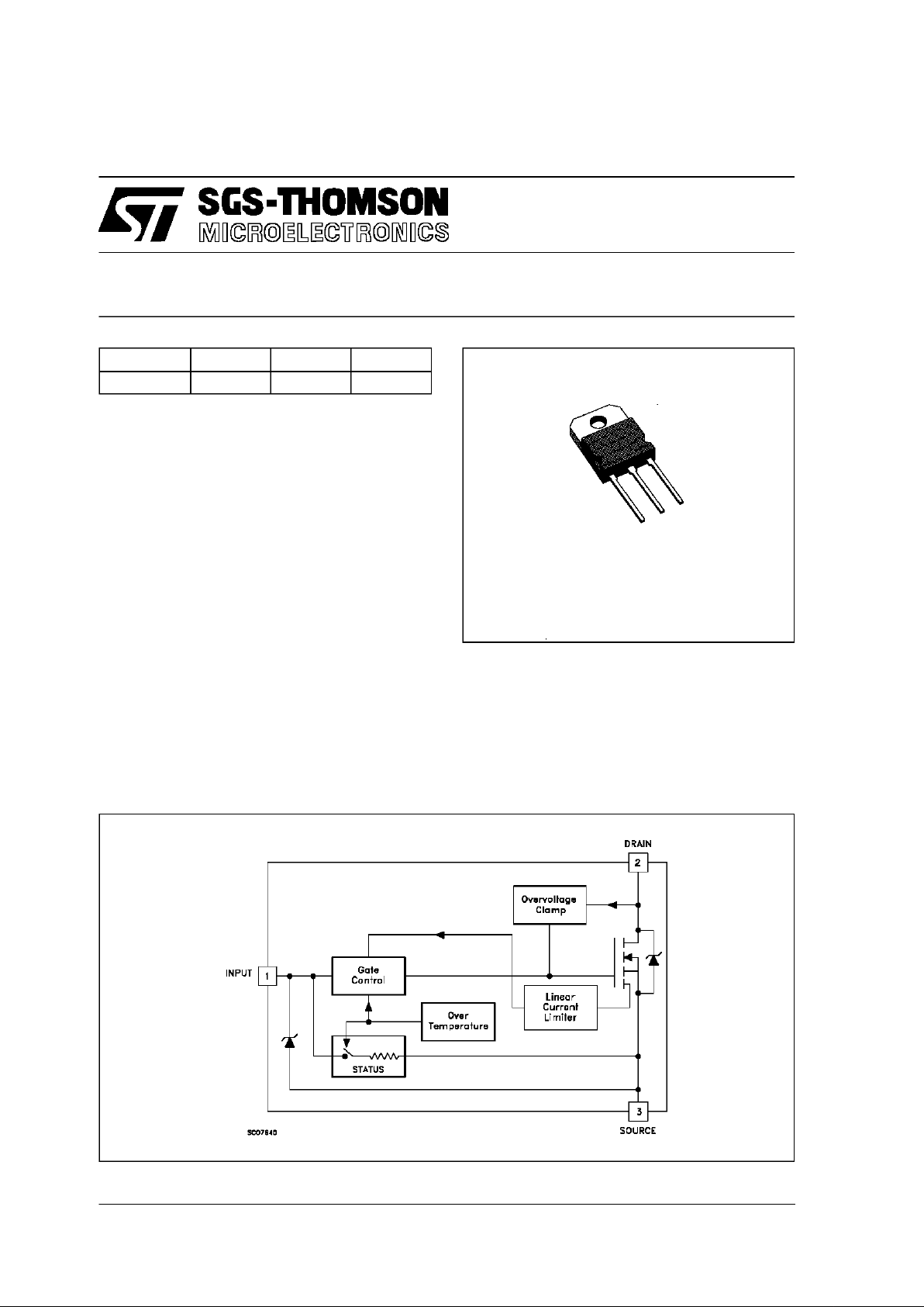
BLOCK DIAGRAM
TYPE V
clamp
R
DS(on)
I
lim
VNH100 N04 42 V 0.012 Ω 100 A
■ LINEAR CURRENT LIMITATION
■ THERMAL SHUT DOWN
■ SHORT CIRCUIT PROTECTION
■ INTEGRATED CLAMP
■ LOW CURRENT DRAWN FROM INPUT PIN
■ DIAGNOSTIC FEEDBACKTHROUGH INPUT
PIN
■ ESD PROTECTION
■ DIRECT ACCESS TO THE GATE OF THE
POWER MOSFET (ANALOG DRIVING)
■ COMPATIBLE WITH STANDARD POWER
MOSFET
■ STANDARD TO-218 PACKAGE
DESCRIPTION
The VNH100N04 is a monolithic device made
using SGS-THOMSON Vertical Intelligent Power
M0 Technology, intended for replacement of
standard power MOSFETS in DC to 50 KHz
applications. Buit-in thermal shut-down, linear
current limitation and overvoltage clamp protect
the chip in harsh enviroments.
Fault feedback can be detected by monitoring the
voltage at the input pin.
TO-218
1/7
Page 2

ABSOLUTE MAXIMUM RATING
Symb o l Parameter Val u e Unit
V
DS
Drain - source Voltage (Vin= 0) Inte r nally Clamp ed V
V
in
Input Voltage 18 V
I
D
Drain C ur rent Inte r nally Limit ed A
I
R
Reverse DC O utput Current -50 A
V
esd
Electrost at ic D is c h ar ge (C= 100 p F , R=1. 5 KΩ ) 2000 V
P
tot
Total Dissipation at Tc=25oC208W
T
j
Oper at ing Junction Temperat ure Inte r nally Limit ed
o
C
T
c
Case Operating Temperature Internally Limited
o
C
T
stg
St orage Temperature -55 to 150
o
C
THERMAL DATA
R
thj-case
R
thj-amb
Thermal Resistance Junc tion-c as e Max
Thermal Resistance Junction- ambient Max
0.6
30
o
C/W
o
C/W
ELECTRICAL CHARACTERISTICS (T
case
=25oC unless otherwise specified)
OFF
Symbol Parameter Test Condi tions Min. Typ. Max. Unit
V
CLAMP
Drain - source Clamp
Volt age
ID=30A Vin= 0 36 42 48 V
V
CLTH
Drain - source Clamp
Thr e s hold Voltage
ID=2mA Vin=0 35 V
V
INCL
Input-Source Rev ers e
Clam p V oltage
Iin=-1mA -1 -0.3 V
I
DSS
Zero Input V oltage
Drain C ur rent (V
in
=0)
V
DS
=13V
V
DS
=25V
50
200
µA
µA
I
ISS
Supply Current f rom
Input Pin
VDS=0V Vin= 10 V 250 500 µ A
ON (∗)
Symbol Parameter Test Condi tions Min. Typ. Max. Unit
V
IS(th)
Input Threshold
Volt age
VDS=VinID=1mA 0.8 3 V
R
DS(on)
St at ic Dr ain- source On
Resistance
Vin=10V ID=30A
V
in
=5V ID=30A
0.012
0.015ΩΩ
DYNAMIC
Symbol Parameter Test Condi tions Min. Typ. Max. Unit
g
fs
(∗)Forward
Tr ansconduct anc e
VDS=13V ID=30A 40 S
C
oss
Out put Cap ac itance VDS=13V f=1MHz Vin= 0 1800 3000 pF
VNH100N04
2/7
Page 3

ELECTRICAL CHARACTERISTICS (continued)
SWITCHING
Symbol Parameter Test Condi tions Min. Typ. Max. Unit
t
d(on)
t
r
t
d(off)
t
f
Turn-on Delay Time
Rise Time
Tur n - of f Delay Time
Fall Time
VDD=15V Id=30A
V
gen
=10V R
gen
=10Ω
(see figure 3)
100
400
900
400
TBD
TBD
TBD
TBD
ns
ns
ns
ns
t
d(on)
t
r
t
d(off)
t
f
Turn-on Delay Time
Rise Time
Tur n - of f Delay Time
Fall Time
VDD=15V Id=30A
V
gen
=10V R
gen
=10Ω
T
j
=125oC
(see figure 3)
TBD
TBD
TBD
TBD
ns
ns
ns
ns
t
d(on)
t
r
t
d(off)
t
f
Turn-on Delay Time
Rise Time
Tur n - of f Delay Time
Fall Time
VDD=15V Id=30A
V
gen
=10V R
gen
=1000Ω
(see figure 3)
TBD
TBD
TBD
TBD
µs
µs
µs
µs
(di/dt)
on
Turn-on Current S lope VDD=15V ID=30A
Vin=10V
TBD A/µs
Q
g
Total Gate Charge VDD=12V ID=30A Vin=10V TBD nC
SOURCE DRAIN DIODE
Symbol Parameter Test Condi tions Min. Typ. Max. Unit
V
SD
(∗) Forward O n Voltage ISD=30A Vin=0 TBD V
t
rr
Q
rr
I
RRM
Reverse Recover y
Time
Reverse Recover y
Charge
Reverse Recover y
Current
ISD= 30 A di/dt = 100 A/µs
VDD=V Tj= 150oC
(see test circuit, figure 5)
TBD
TBD
TBD
ns
µC
A
PROTECTION
Symbol Parameter Test Condi tions Min. Typ. Max. Unit
I
lim
Drain C ur rent Limit Vin=10V VDS= 13 V 70 100 140 A
t
dlim
St ep Response
Current Limit
Vin=10V VDS=13V TBD µs
T
jsh
Overtemperature
Shut down
150 170 190
o
C
T
jrs
Ove rtempe rature Rese t 135
o
C
I
gf
Fault Sink Cu r rent Vin=10V VDS=13V 50 mA
E
as
Single Pulse
Avalanc he Ener gy
starting Tj=25oCVDD=20V
Vin=10V R
gen
=1KΩ L= mH
TBD J
(∗) Puls ed: Pulse dur ation = 300 µs, duty cycle 1.5 %
VNH100N04
3/7
Page 4

During normal operation, the Input pin is
electrically connected to the gate of the internal
power MOSFET. The device then behaves like a
standard power MOSFET and can be used as a
switch from DC to 50 KHz. The only difference
from the user’s standpoint is that a small DC
current (I
iss
) flows into the Input pin in order to
supply the internal circuitry.
The device integrates:
– OVERVOLTAGE CLAMP PROTECTION:
internally set at 42V, along with the rugged
avalanche characteristics of the Power
MOSFET stage give this device unrivalled
ruggedness and energy handling capability.
This feature is mainly important when driving
inductive loads.
– LINEAR CURRENT LIMITER CIRCUIT: limits
the drain current Id to Ilim whatever the Input
pin voltage. When the current limiter is active,
the device operates in the linear region, so
power dissipation may exceed the capability of
the heatsink. Both case and junction
temperatures increase, and if this phase lasts
long enough, junction temperature may reach
the overtemperature threshold T
jsh
.
– OVERTEMPERATURE AND SHORT CIRCUIT
PROTECTION: these are based on sensing
the chip temperature and are not dependent on
the input voltage. The location of the sensing
element on the chip in the power stage area
ensures fast, accurate detection of the junction
temperature. Overtemperature cutout occurs in
the range 150 to 190oC, a typical value being
170oC. The device is automatically restarted
when the chip temperature falls below 135oC.
– STATUS FEEDBACK: In the case of an
overtemperature fault condition, a Status
Feedback is provided through the Input pin.
The internal protection circuit disconnects the
input from the gate and connects it instead to
ground via an equivalent resistance of 200 Ω.
The failure can be detected by monitoring the
voltage at the Input pin, which will be close to
ground potential.
Additional features of this device are ESD
protection according to the Human Body model
and the ability to be driven from a TTL Logic
circuit (with a small increase in R
DS(on)
).
PROTECTION FEATURES
VNH100N04
4/7
Page 5

Fig. 2: Unclamped Inductive Waveforms
Fig. 3: Switching Times Test Circuits For
Resistive Load
Fig. 4: Input Charge Test Circuit
Fig. 1: Unclamped Inductive Load Test Circuits
Fig. 5: Test Circuit For Inductive Load Switching
And Diode Recovery Times
Fig. 6: Waveforms
VNH100N04
5/7
Page 6

DIM.
mm inch
MIN. TYP. MAX. MIN. TYP. MAX.
A 4.7 4.9 0.185 0.193
C 1.17 1.37 0.046 0.054
D 2.5 0.098
E 0.5 0.78 0.019 0.030
F 1.1 1.3 0.043 0.051
G 10.8 11.1 0.425 0.437
H 14.7 15.2 0.578 0.598
L2 – 16.2 – 0.637
L3 18 0.708
L5 3.95 4.15 0.155 0.163
L6 31 1.220
R – 12.2 – 0.480
Ø 4 4.1 0.157 0.161
R
A
C
D
E
H
F
G
L6
Ø
L3
L2
L5
123
TO-218 (SOT-93) MECHANICAL DATA
P025A
VNH100N04
6/7
Page 7

Information furnished is believed to be accurateand reliable. However, SGS-THOMSON Microelectronics assumes no responsability for the
consequences of use of such informationnor for any infringement of patents or other rights of third partieswhich may results from its use. No
license isgranted by implication or otherwiseunder anypatent orpatent rights of SGS-THOMSON Microelectronics.Specificationsmentioned
in this publicationare subject to changewithout notice. This publication supersedes and replaces all information previously supplied.
SGS-THOMSON Microelectronicsproducts arenotauthorizedfor use ascriticalcomponents in lifesupportdevices orsystemswithout express
written approvalof SGS-THOMSON Microelectonics.
1994 SGS-THOMSON Microelectronics- All RightsReserved
SGS-THOMSON Microelectronics GROUP OFCOMPANIES
Australia - Brazil - France - Germany - Hong Kong -Italy - Japan - Korea - Malaysia -Malta - Morocco - The Netherlands -
Singapore -Spain - Sweden - Switzerland -Taiwan - Thailand - UnitedKingdom - U.S.A
VNH100N04
7/7
 Loading...