

Page 1
®
July 2002 1/18
VND810SP
DOUBLE CHANNEL HIGH SIDE DRIVER
1
■ CMOS COMPATIBLE INPUTS
■ OPEN DRAIN STATUS OUTPUTS
■ ON STATE OPEN LOAD DETECTION
■ OFF STATE OPEN LOAD DETECTION
■ SHORTED LOAD PROTECTION
■ UNDERVOLTAGE AND OVERVOLTAGE
SHUTDOWN
■ PROTECTION AGAINST LOSS OF GROUND
■ VERY LOW STAND-BY CURRENT
■ REVERSE BATTERY PROTECTIO N (**)
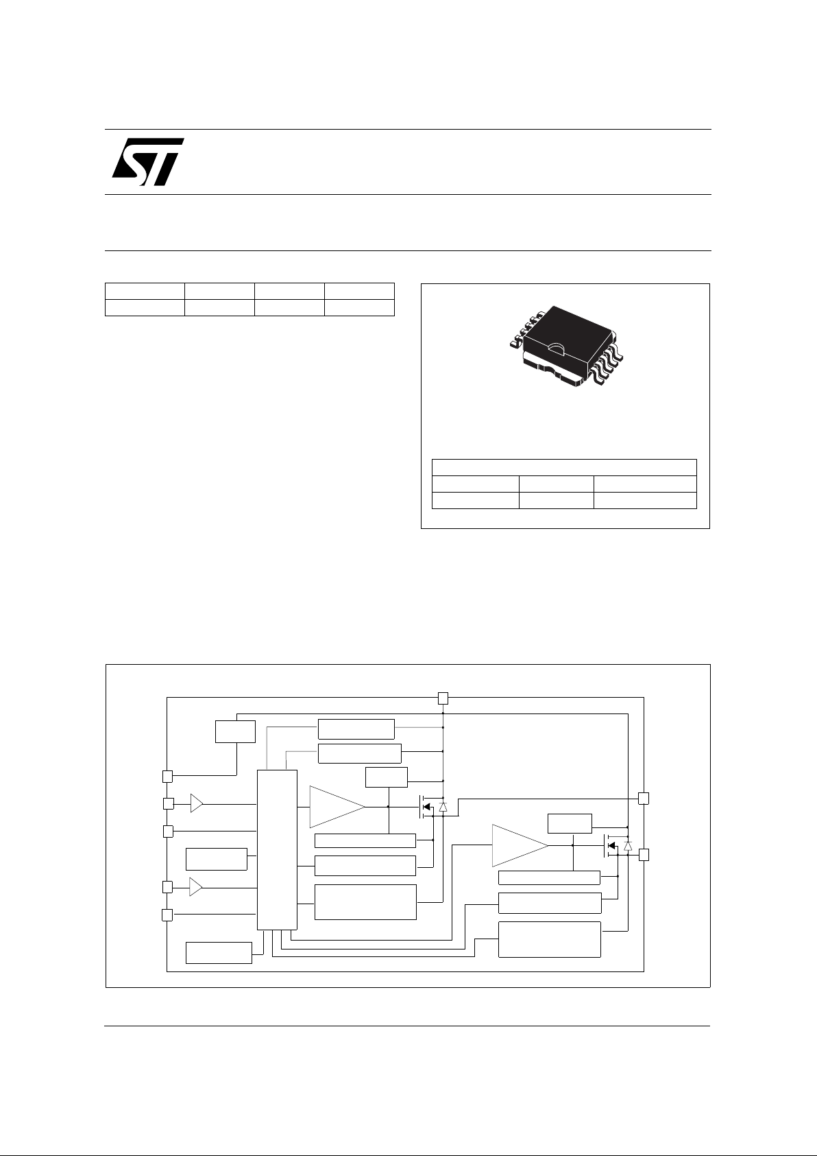
DESCRIPTION
The VND810 SP is a monolithic de vice made by
using STMicroelectronics VIPower M0-3
Technology, intende d for d riving any k ind of l oad
with one side connected to ground.
Active VCC pin voltag e clamp protects th e dev ice
against low energy spikes (see ISO7637 transient
compatibility table). Active current limitation
combined with thermal sh utdown and automatic
restart protects the device against overloa d. The
device detects open load condition both in on and
off state. Output shorted to VCC is detected in the
off state. Dev ice auto mati cally tur ns off in c ase of
ground pin disconnection.
TYPE R
DS(on)
I
OUT
V
CC
VND810 SP 160 mΩ (*) 3.5 A (*) 36 V
1
10
PowerSO-10
™
ORDER CODES
PACKAGE TU B E T&R
PowerSO-10™ VND810SP VND810SP13TR
(*) Per each channel
BLOCK DIAGRAM
(**) See appl ic ation schema tic at page 8
OVERTEMP. 1
V
cc
GND
INPUT1
OUTPUT1
OVERVOLTAGE
LOGIC
DRIVER 1
STATUS1
V
cc
CLAMP
UNDERVOLTAGE
CLAMP 1
OPENLOAD ON 1
CURRENT LIMITER 1
OPENLOAD OFF 1
OUTPUT2
DRIVER 2
CLAMP 2
OPENLOAD ON 2
OPENLOAD OFF 2
OVERTEMP. 2
INPUT2
STATUS2
CURRENT LIMITER 2
Page 2
2/18
VND810SP
ABSOLUTE MAXIMUM RATI NG
CONNECTION DIAGRAM (TOP VIEW)
Symbol Parameter Value Unit
V
CC
DC Supply Voltage 41 V
- V
CC
Reverse DC Supply Voltage - 0.3 V
- I
GND
DC Reverse Ground Pin Current - 200 mA
I
OUT
DC Output Current Internally Limited A
- I
OUT
Reverse DC Output Current - 6 A
I
IN
DC Input Curr ent +/- 10 mA
I
stat
DC Status Cur rent +/- 10 mA
V
ESD
Electros tatic Discharge (Human Body Model: R=1.5KΩ; C=100pF)
- INPUT
- STATUS
- OUTPU T
- V
CC
4000
4000
5000
5000
V
V
V
V
E
MAX
Maximum Switching Energy
(L=1.4mH; R
L
=0Ω; V
bat
=13.5V; T
jstart
=150ºC; IL=5A)
24 mJ
P
tot
Powe r Dissipation TC=25°C 52 W
T
j
Junction Operating Temperature Internally Limited °C
T
c
Case Operating Temperature - 40 to 150 °C
T
stg
Storage Temperature - 55 to 150 °C
1
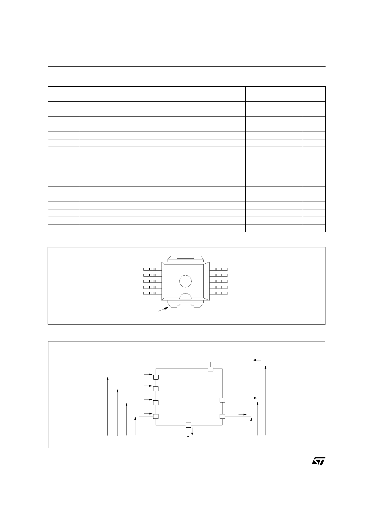
CURRENT AND VOLTAGE CO NVENTIONS
1
2
3
4
5
6
7
8
9
10
11
OUTPUT 1
OUTPUT 1
N.C.
OUTPUT 2
OUTPUT 2
GROUND
INPUT 1
STATUS 1
STATUS 2
INPUT 2
V
CC
I
S
I
GND
OUTPUT 2
V
CC
GND
STATUS 2
INPUT 2
I
OUT2
I
IN2
I
STAT2
V
STAT2
V
IN2
V
CC
V
OUT2
OUTPUT 1
I
OUT1
V
OUT1
INPUT 1
I
IN1
STATUS 1
I
STAT1
V
IN1
V
STAT1
Page 3

3/18
VND810SP
THERMAL DATA
(*) When mounted on a standard single-sided FR-4 board with 0.5cm2 of Cu (at least 35µm thick). Horizontal mounting and no artificial air
flow.
ELECTRICAL CHARACTERISTICS (8V<VCC<36V; -40°C< Tj < 150°C, unless otherwise specified)
(Per each channel)
POWER OUTPUTS
(**) Per device
SWITCHING (VCC=13V)
LOGIC INPUT
Symbol Parameter Value Unit
R
thj-case
Thermal R esistance Junction- case 2.4 °C/W
R
thj-amb
Thermal Resistance Junction-ambient 52.4 (*) °C/W
Symbol Parameter Test Conditions Min Typ Max Unit
V
CC
(**) Operating Supply Voltage 5.5 13 36 V
V
USD
(**) Undervoltage Shut-down 3 4 5.5 V
V
OV
(**) Ove rvoltage Shu t-down 36 V
R
ON
On State Resistance
I
OUT
=1A; Tj=25°C
I
OUT
=1A; VCC>8V
160
320
mΩ
mΩ
I
S
(**) Supply Current
Off State; V
CC
=13V; VIN=V
OUT
=0V
Off State; V
CC
=13V; VIN=V
OUT
=0V;
Tj=25°C
On State; V
CC
=13V; VIN=5V; I
OUT
=0A
12
12
5
40
25
7
µA
µA
mA
I
L(off1)
Off State Output Current VIN=V
OUT
=0V 0 50 µA
I
L(off2)
Off State Output Current VIN=0V; V
OUT
=3.5V -75 0 µA
I
L(off3)
Off State Output Current VIN=V
OUT
=0V; Vcc=13V; Tj =125°C 5 µA
I
L(off4)
Off State Output Current VIN=V
OUT
=0V; Vcc=13V; Tj =25°C 3 µA
Symbol Parame ter Test Condit ions Min Typ Max Unit
t
d(on)
Turn-on Delay Time
RL=13Ω from VIN rising edge to
V
OUT
=1.3V
30 µs
t
d(off )
Turn-off Delay Time
RL=13Ω from VIN falling edge to
V
OUT
=11.7V
30 µs
dV
OUT
/
dt
(on)
Turn-on Voltage Slope
RL=13Ω from V
OUT
=1.3V to
V
OUT
=10.4V
See
relative
diagram
V/µs
dV
OUT
/
dt
(off)
Turn-off Voltage Slop e
RL=13Ω from V
OUT
=11.7V to
V
OUT
=1.3V
See
relative
diagram
V/µs
Symbol Param eter Test Conditions Min Typ Max Unit
V
IL
Input Low Level 1.25 V
I
IL
Low Level Input Current VIN = 1.25V 1 µA
V
IH
Input High Level 3.25 V
I
IH
High Level Input Current VIN = 3.25V 10 µA
V
hyst
Input Hyst eresis Voltage 0.5 V
V
ICL
Input Clamp Voltage
I
IN
= 1mA
I
IN
= -1mA
66.8
-0.7
8V
V
1
Page 4

4/18
VND810SP
ELECTRICAL CHARACTERISTICS (continued)
STATUS PIN
PROTECTIONS
OPENLOAD DETECTION
Symbol Parameter Test Conditions Min Typ Max Unit
V
STAT
Status Low Output Voltage I
STAT
= 1.6 mA 0.5 V
I
LSTAT
Status Leakage Current Normal Operation; V
STAT
= 5V 10 µA
C
STAT
Status Pin Input
Capacitance
Normal Operation; V
STAT
= 5V 100 pF
V
SCL
Status Clamp Voltage
I
STAT
= 1mA
I
STAT
= - 1mA
66.8
-0.7
8V
V
Symbol Parame ter Test Condit ions Min Typ Max Unit
T
TSD
Shut-down Temperature 150 175 200 °C
T
R
Reset Temp erature 135 °C
T
hyst
Ther ma l Hy steresi s 7 15 °C
t
sdl
Status Delay in Overload
Conditions
Tj>T
TSD
20 µs
I
lim
Current limitation
5.5V<V
CC
<36V
3.5 5 7.5
7.5
A
A
V
demag
Turn-off Output Clamp
Voltage
I
OUT
=1A; L= 6m H VCC-41 VCC-48 VCC-55 V
Symbol Param eter Test Conditions Min Typ Max Unit
I
OL
Openload ON State
Detectio n Threshold
V
IN
=5V 20 40 80 mA
t
DOL(on)
Openload ON State
Detection Delay
I
OUT
=0A 200 µs
V
OL
Openload OFF State
Voltage Detection
Threshold
VIN=0V 1.5 2.5 3.5 V
t
DOL(off)
Openload Detection Delay
at Turn Off
1000 µs
2
1
V
INn
V
STAT n
t
DOL(off)
OPEN LOAD STATUS TIMING (with external pull-up)
V
INn
V
STAT n
OVER TEMP STATUS TIMING
t
SDL
t
SDL
I
OUT
< I
OL
V
OUT
> V
OL
t
DOL(on)
Tj > T
TSD
Page 5
5/18
VND810SP
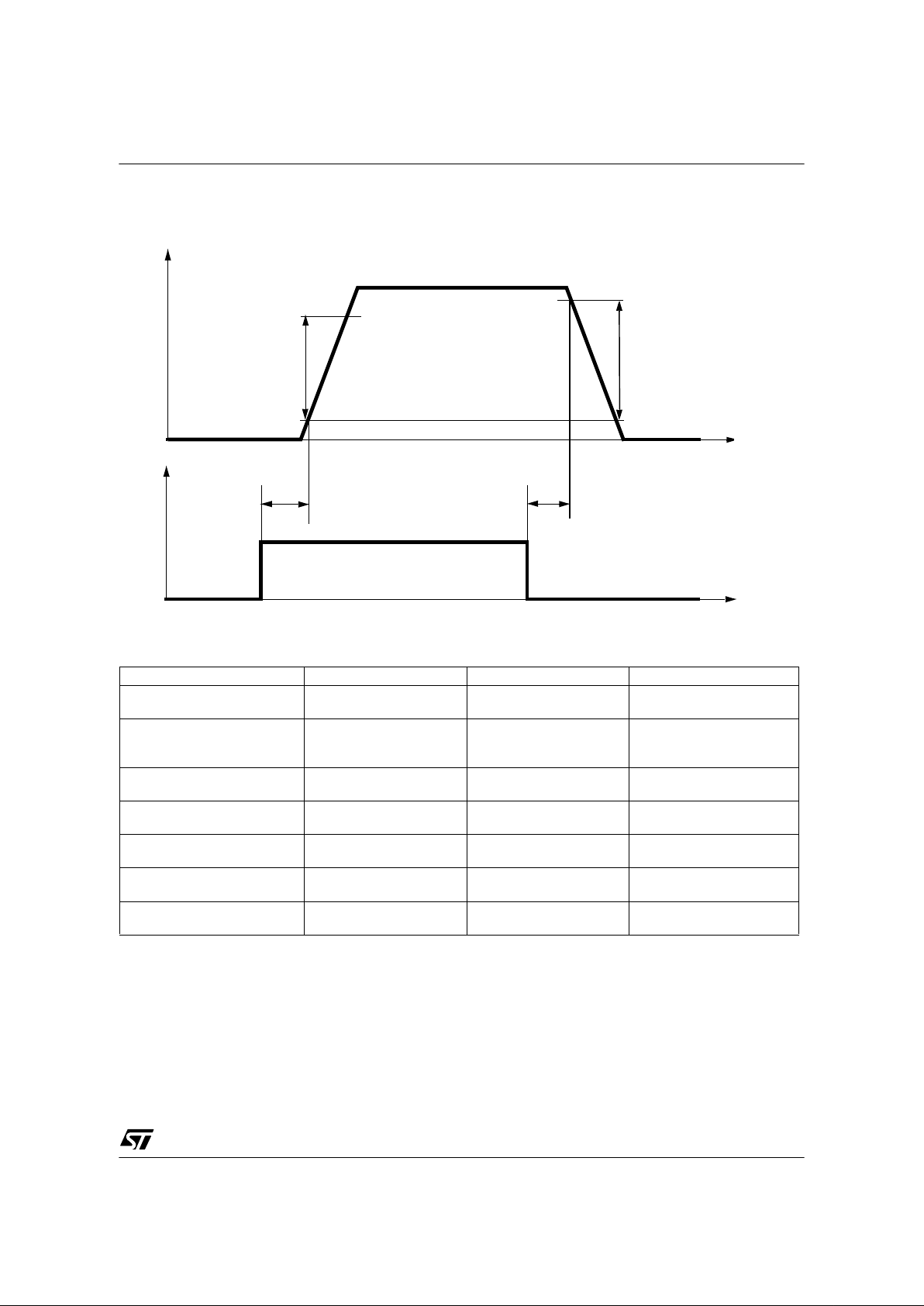
1
t
t
V
OUTn
V
INn
80%
10%
dV
OUT
/dt
(on)
t
d(off)
90%
dV
OUT
/dt
(off)
t
d(on)
Switching time Waveforms
TRUTH TABLE
CONDITIONS INPUT OUTPUT STATUS
Normal Operation
L
H
L
H
H
H
Current Limitation
L
H
H
L
X
X
H
(T
j
< T
TSD
) H
(T
j
> T
TSD
) L
Overtemperature
L
H
L
L
H
L
Undervoltage
L
H
L
L
X
X
Overvoltage
L
H
L
L
H
H
Output Voltage > V
OL
L
H
H
H
L
H
Output Current < I
OL
L
H
L
H
H
L
Page 6
6/18
VND810SP
1
1
ELECTRICAL TRANS IENT REQUIREMENTS ON VCC PIN
ISO T/R 7637/1
Test Pulse
TEST LEVELS
I II III IV Delays and
Impedance
1 -25 V -50 V -75 V -100 V 2 ms 10 Ω
2 +25 V +50 V +75 V +100 V 0.2 ms 10 Ω
3a -25 V -50 V -100 V -150 V 0.1 µs 50 Ω
3b +25 V +50 V +75 V +100 V 0.1 µs 50 Ω
4 -4 V -5 V -6 V -7 V 100 ms, 0.01
Ω
5 +26.5 V +46.5 V +66.5 V +86.5 V 400 ms, 2
Ω
ISO T/R 7637/1
Test Pulse
TEST LEVELS RESULTS
IIIIIIIV
1CCCC
2CCCC
3aCCCC
3bCCCC
4CCCC
5CEEE
CLASS CONTENTS
C All functions of the device are perform e d as designe d after expos ure to distu rb ance.
E One or more functions of the device is not performed as designed after exp osure and cannot be
returned to proper operation without rep lacing the device.
Page 7

7/18
VND810SP
1
OPEN LOAD without external pull-up
STATUS
n
INPUT
n
NORMAL OPERATION
UNDERVOLTAGE
V
CC
V
USD
V
USDhyst
INPUT
n
OVERVOLTAGE
V
CC
STATUS
n
INPUT
n
STATUS
n
STATUS
n
INPUT
n
STATUS
n
INPUT
n
OPEN LOAD wi th external pull-up
undefined
OVERTEMPE RATURE
INPUT
n
STATUS
n
T
TSD
T
R
Figure 1: Waveforms
T
j
OUTPUT VOLTAGE
n
VCC<V
OV
OUTPUT VOLTAGE
n
OUTPUT VOLTAGE
n
OUTPUT VOLTAGE
n
OUTP U T VO LTAGE
n
OUTPUT CURRENT
n
V
OUT>VOL
V
OL
VCC>V
OV
Page 8

8/18
VND810SP
GND PROTECTION NETWORK AGAINST
REVERSE BATTERY
Soluti on 1: Resistor in the ground line (R
GND
only). This
can be us ed with any type of load.
The fo llowin g is an indica tion on how to dim ension the
R
GND
resistor.
1) R
GND
≤ 600mV / I
S(on)max
.
2) R
GND
≥ (− VCC) / (-I
GND
)
where -I
GND
is the DC re vers e grou nd pi n cu rren t an d can
be found in the absolute maximum rating section of the
device’s datasheet.
Power Dissipation in R
GND
(when VCC<0: during reverse
battery situations) is:
P
D
= (-VCC)2/R
GND
This resistor can be shared amongst several different
HSD. Please note that the val u e of this resi s to r sh ou l d be
calcul ated with form ula (1) wher e I
S(on)max
becomes t he
sum of the maximum on-state currents of the different
devices.
Please note that if the microprocessor ground is not
common with the device ground then the R
GND
will
produce a shift (I
S(on)max
* R
GND
) in the input thresholds
and the status output values. This shift will vary
depending on how man y devic es are ON in the ca se of
several high side dr ivers shari ng the same R
GND
.
If the calculated power dissipation leads to a large resistor
or seve ral de vic es have to s hare t he s ame r esisto r then
the ST suggests to utili ze Solution 2 (see below).
Solution 2:
A diode (D
GND
) in the gro und line.
A resistor (R
GND
=1kΩ) should be inserted in parallel to
D
GND
if the devi ce will be driving an inductive load.
This small signal diode can be safely shared amongst
several different HSD. Also in this case, the presence of
the ground network wi ll produce a shift (
j
600mV) in t he
input threshold and the status output values if the
microprocessor ground is not common with the device
ground. This shift will not vary if more than one HSD
shares the same diod e/resisto r network.
LOAD DUMP PROTECTION
Dld is necessary (Voltage Transient Suppressor) if the
load dump peak voltage exceeds VCC max DC rating. The
same applies if the device will be subject to transients on
the VCC line that are grea ter tha n the ones sh own in the
ISO T/R 7637/1 table.
1
APPLICATION SCHEMATIC
1
V
CC
OUTPUT2
D
ld
+5V
R
prot
OUTPUT1
STA T US1
INPUT1
+5V
STA TUS2
INPUT2
GND
+5V
µ
C
R
prot
R
prot
R
prot
D
GND
R
GND
V
GND
Page 9

9/18
VND810SP
1
µ
C I/Os PROTECTION:
If a ground protection network is used and negative
transient are pr esent on the VCC line, the control pins will
be pulled negative. ST suggests to insert a resistor (R
prot
)
in line to prevent the µC I/Os pins to latch-up.
The valu e of these res istors is a compromise between
the leakage current of µC and the current required by the
HSD I/Os (Input levels compatibility) with the latch-up limit
of µC I/Os.
-V
CCpeak/Ilatchup
≤ R
prot
≤ (V
OHµC-VIH-VGND
) / I
IHmax
Calcu lation example:
For V
CCpeak
= - 100V and I
latchup
≥ 20mA; V
OHµC
≥ 4.5V
5kΩ ≤ R
prot
≤ 65kΩ .
Recomm ended R
prot
value is 10kΩ.
OPEN LOAD DETECTION IN OFF STATE
Off state open load detection requires an external pull-up
resistor (R
PU
) connected between OUTPUT pin and a
positive supply voltage (V
PU
) like the +5 V line used to
supply the microprocessor.
The exter na l res i stor ha s to be s ele ct ed ac cor d ing t o th e
follow i n g re quiremen ts:
1) no fal s e ope n l oad in dica t ion w he n l oad is conn ec ted:
in this c ase we ha ve to av oid V
OUT
to be high er tha n
V
Olmin
; this results in the following condition
V
OUT
=(VPU/(RL+RPU))RL<V
Olmin.
2) no misdetection when load is disconnected: in this
case the V
OUT
has to be higher than V
OLmax
; this
results in the following condition R
PU
<(V
PU–VOLma x
)/
I
L(off2)
.
Beca us e I
s(OFF)
may si gn ifi c a ntly incr ea se i f V
out
is pulled
high (up t o several mA ), the pul l-up resi stor R
PU
should
be conne cted t o a su pp ly t ha t is swit ch ed OFF when t h e
module is in standby.
The values of V
OLmin
, V
OLmax
and I
L(off2)
are available in
the Electrical Cha racteristics section.
V
OL
V batt. VPU
R
PU
R
L
R
DRIVER
+
LOGIC
+
-
INPUT
STATUS
V
CC
OUT
GROUND
I
L(off2)
Open Load detection in off state
Page 10

10/18
VND810SP
1
High Level Input Current
Input Clamp Voltage Status Leakage Current
Off State Output Current
Status Clamp VoltageStatus Low Output Voltage
-50 -25 0 25 50 75 100 125 150 175
Tc (°C)
0
0.5
1
1.5
2
2.5
3
3.5
4
4.5
5
Iih (uA)
Vin=3.25V
-50 -25 0 25 50 75 100 125 150 175
Tc (°C)
6
6.2
6.4
6.6
6.8
7
7.2
7.4
7.6
7.8
8
Vicl (V)
Iin=1mA
-50 -25 0 25 50 75 100 125 150 175
Tc (°C)
0
0.01
0.02
0.03
0.04
0.05
Ilstat (uA)
Vstat=5V
-50 -25 0 25 50 75 100 125 150 175
Tc (°C)
0
0.1
0.2
0.3
0.4
0.5
0.6
0.7
0.8
Vstat (V)
Istat=1.6mA
-50 -25 0 25 50 75 100 125 150 175
Tc (°C)
6
6.2
6.4
6.6
6.8
7
7.2
7.4
7.6
7.8
8
Vscl (V)
Istat=1mA
-50 -25 0 25 50 75 100 125 150 175
Tc (ºC)
0
0.16
0.32
0.48
0.64
0.8
0.96
1.12
1.28
1.44
1.6
IL(off1) (uA)
Off state
Vcc=36V
Vin=Vout=0V
Page 11

11/18
VND810SP
1
Input Hysteresis VoltageInput Low Level
On State Resistance Vs T
case
On State Resistance Vs V
CC
Input High LevelOpenload On State Detection Threshold
-50 -25 0 25 50 75 100 125 150 175
Tc (°C)
2
2.2
2.4
2.6
2.8
3
3.2
3.4
3.6
Vih (V)
-50 -25 0 25 50 75 100 125 150 175
Tc (°C)
1
1.2
1.4
1.6
1.8
2
2.2
2.4
2.6
Vil (V)
-50 -25 0 25 50 75 100 125 150 175
Tc (°C)
0.5
0.6
0.7
0.8
0.9
1
1.1
1.2
1.3
1.4
1.5
Vhyst (V)
-50 -25 0 25 50 75 100 125 150 175
Tc (ºC)
0
50
100
150
200
250
300
350
400
Ron (mOhm)
Iout=1A
Vcc=8V; 13V & 36V
5 10152025303540
Vcc (V)
0
50
100
150
200
250
300
350
400
Ron (mOhm)
Iout=1A
Tc= - 40ºC
Tc= 25ºC
Tc= 125ºC
-50 -25 0 25 50 75 100 125 150 175
Tc (°C)
10
15
20
25
30
35
40
45
50
55
60
Iol (mA)
Vcc=13V
Vin=5V
Page 12

12/18
VND810SP
1
Overvoltage Shutdown
Turn-on Voltage Slope Turn-off Voltage Slope
I
LIM
Vs T
case
Openload Off State Voltage Detection Threshold
-50 -25 0 25 50 75 100 125 150 175
Tc (°C)
30
32
34
36
38
40
42
44
46
48
50
Vov (V)
-50 -25 0 25 50 75 100 125 150 175
Tc (°C)
0
0.5
1
1.5
2
2.5
3
3.5
4
4.5
5
Vol (V)
Vin=0V
-50 -25 0 25 50 75 100 125 150 175
Tc (ºC)
0
100
200
300
400
500
600
700
800
900
1000
dVout/dt(on) (V/ms)
Vcc=13V
Rl=13Ohm
-50 -25 0 25 50 75 100 125 150 175
Tc (ºC)
0
50
100
150
200
250
300
350
400
450
500
dVout/dt(off) (V/ms)
Vcc=13V
Rl=13Ohm
-50 -25 0 25 50 75 100 125 150 175
Tc (°C)
0
1
2
3
4
5
6
7
8
9
10
Ilim (A)
Vcc=13V
Page 13

13/18
VND810SP
Maximum turn off current versus load inductance
A = Single Pulse at T
Jstart
=150ºC
B= Repetitive pulse at T
Jstart
=100ºC
C= Repetitive Pulse at T
Jstart
=125ºC
Conditions:
VCC=13.5V
Values are generated with RL=0Ω
In case of repetitive pulses, T
jstart
(at beginning of each demagnetization) of every pulse must not exceed
the temperature specified above for curves B and C.
VIN, I
L
t
Demagnetization
Demagnetization
Demagnetization
1
10
0.01 0.1 1 10 100
L(mH)
I
LMAX (A)
A
B
C
Page 14

14/18
VND810SP
PowerSO-10™ PC Board
R
thj-amb
Vs PCB copper area in open box free air condition
PowerSO-10™ THERMAL DATA
Layout condition of Rth and Zth measurements (PCB FR4 area= 58mm x 58m m , PCB thickn ess=2mm,
Cu thickness=35µm, Copper areas: from minimum pad lay-out to 8cm
2
).
30
35
40
45
50
55
0246810
PCB Cu heatsink area (cm^2)
RTHj_amb (°C/W)
Tj-Tamb=50°C
Page 15

15/18
VND810SP
Thermal fitting model of a double channel HSD
in PowerSO-10
Pulse calculation formula
Thermal Parameter
Area/island (cm2)0.56
R1 (°C/W) 0.35
R2 (°C/W) 1.8
R3( °C/W) 1.1
R4 (°C/W) 0.8
R5 (°C/W) 12
R6 (°C/W) 37 22
C1 (W.s/°C) 0.0001
C2 (W.s/°C) 7.00E-04
C3 (W.s/°C) 0.008
C4 (W.s/°C) 0.3
C5 (W.s/°C) 0.75
C6 (W.s/°C) 3 5
Z
THδ
RTHδ Z
THtp
1 δ–()+⋅=
where
δ tpT⁄=
PowerSO-10 Thermal Impedance Junction Ambient Single Pulse
0.1
1
10
100
1000
0.0001 0.001 0.01 0.1 1 10 100 1000
Time (s)
ZTH (°C/W)
0.5 cm
2
6 cm
2
T_amb
Pd1
C1
R4
C3 C4
R3R1 R6R5R2
C5 C6C2
Pd2
R2
C1 C2
R1
Tj_1
Tj_2
Page 16

16/18
VND810SP
111
1
DIM.
mm. inch
MIN. TYP MAX. MIN. TYP. MAX.
A 3.35 3.65 0.132 0.144
A (*) 3.4 3.6 0.134 0.142
A1 0.00 0.10 0.000 0.004
B 0.40 0.60 0.016 0.024
B (*) 0.37 0.53 0.014 0.021
C 0.35 0.55 0.013 0.022
C (*) 0.23 0.32 0.009 0.0126
D 9.40 9.60 0.370 0.378
D1 7.40 7.60 0.291 0.300
E 9.30 9.50 0.366 0.374
E2 7.20 7.60 0.283 300
E2 (*) 7.30 7.50 0.287 0.295
E4 5.90 6.10 0.232 0.240
E4 (*) 5.90 6.30 0.232 0.248
e 1.27 0.050
F 1.25 1.35 0.049 0.053
F (*) 1.20 1.40 0.047 0.055
H 13.80 14.40 0.543 0.567
H (*) 13.85 14.35 0.545 0.565
h 0.50 0.002
L 1.20 1.80 0.047 0.070
L (*) 0.80 1.10 0.031 0.043
α 0º 8º 0º 8º
α (*) 2º 8º 2º 8º
1
1
PowerSO-10™ MECHANICAL DATA
(*) Muar only POA P013P
DETAIL "A"
PLANE
SEATING
α
L
A1
F
A1
h
A
D
D1
= =
= =
E4
0.10 A
E
C
A
B
B
DETAIL "A"
SEATING
PLANE
E2
10
1
eB
HE
0.25
P095A
Page 17

17/18
VND810SP
1
PowerSO-10™ SUGGESTED PAD LAYOUT
1
TAPE AND REEL SHIPMENT (suf fix “13TR”)
REEL DIMENSIONS
All dimensions are in mm.
Base Q.ty 600
Bulk Q.ty 600
A (max) 330
B (min) 1.5
C (± 0.2) 13
F 20.2
G (+ 2 / -0) 24.4
N (min) 60
T (max) 30.4
TAPE DIMENSIONS
According to Electronic Industries Association
(EIA) Standard 481 rev. A, Feb 1986
All dimensions are in mm.
Tape width W 24
Tape Hole Spacing P0 (± 0.1) 4
Component Spacing P 24
Hole Diameter D (± 0.1/-0) 1.5
Hole Diameter D1 (min) 1.5
Hole Position F (± 0.05) 11.5
Compartm ent Depth K (max) 6.5
Hole Spacing P1 (± 0.1) 2
Top
cover
tape
End
Start
No componentsNo components Components
500mm min
500mm min
Empty components pockets
saled with cover tape.
User direction of feed
6.30
10.8 - 11
14.6 - 14.9
9.5
1
2
3
4
5
1.27
0.67 - 0.73
0.54 - 0.6
10
9
8
7
6
B
A
C
All dimensi ons ar e in mm.
Base Q.ty Bulk Q.ty Tube length (± 0.5) A B C (± 0.1 )
Casablanca 50 1000 532 10. 4 16. 4 0.8
Muar 50 10 00 532 4.9 17.2 0.8
TUBE SHIPMENT (no suffix)
C
A
B
MUARCASABLANCA
Page 18

18/18
VND810SP
Information furnished is believed to be accurate and r eliable. Ho wev er, STMicroelectr onics assume s no r es ponsibility for the consequenc es
of use of such information nor for any infringement of patents or other rights of third parties which may results from its use. No license is
granted by implication or otherwise under a ny patent or patent rights of STMicroelectronics. Specif ic ations mentioned in this publication are
subject to c hange withou t notice. This publication supersed es and replace s all information previous ly s upplied. ST M icroelect r on ics products
are not authorized for use as critical components in life support devices or systems without express written approval of STMicroelectronics.
The ST logo is a trademark of ST M ic r oelectronic s
2002 STMicroelectronics - Printed in ITALY- All Rights Reserved.
STMicroelectronics GROUP OF COMPANIES
Australia - Brazil - Canada - Ch ina - Finland - Franc e - Germany - Hong K ong - India - Isra el - Italy - Japan - M alaysia -
Malta - Moro c c o - S ingapore - Spain - Sweden - Swit z er land - United Kingdom - U.S.A.
http://www.st.com
 Loading...