

Datasheet VND7NV04-1, VND7NV04, VNS7NV04, VNN7NV04 Datasheet (SGS Thomson Microelectronics)
Page 1
®
VNN7NV04 / VNS7NV04
/ VND7NV 04 / VND7NV0 4-1
“OMNIFET II”:
FULLY AUTOPROTECTED POW ER M OSFET
TYPE R
VNN7NV04
VNS7NV04
VND7NV04
VND7NV04-1
n
LINEAR CURRENT LIMITATION
n
THERMAL SHUT DOWN
n
SHORT CIRCUIT PROTECTION
n
INTEGRATED CLAMP
n
LOW CURRENT DRAWN FRO M INPUT PIN
n
DIAGNOSTIC FEEDBACK THROUGH INPUT
DS(on)
60 mΩ 6 A 40 V
I
lim
V
clamp
PIN
n
ESD PROTECTION
n
DIRECT ACCESS TO THE GATE OF THE
POWER MOSFET (ANALOG DRIVING)
n
COMPATIBLE WITH STANDARD POWER
MOSFET
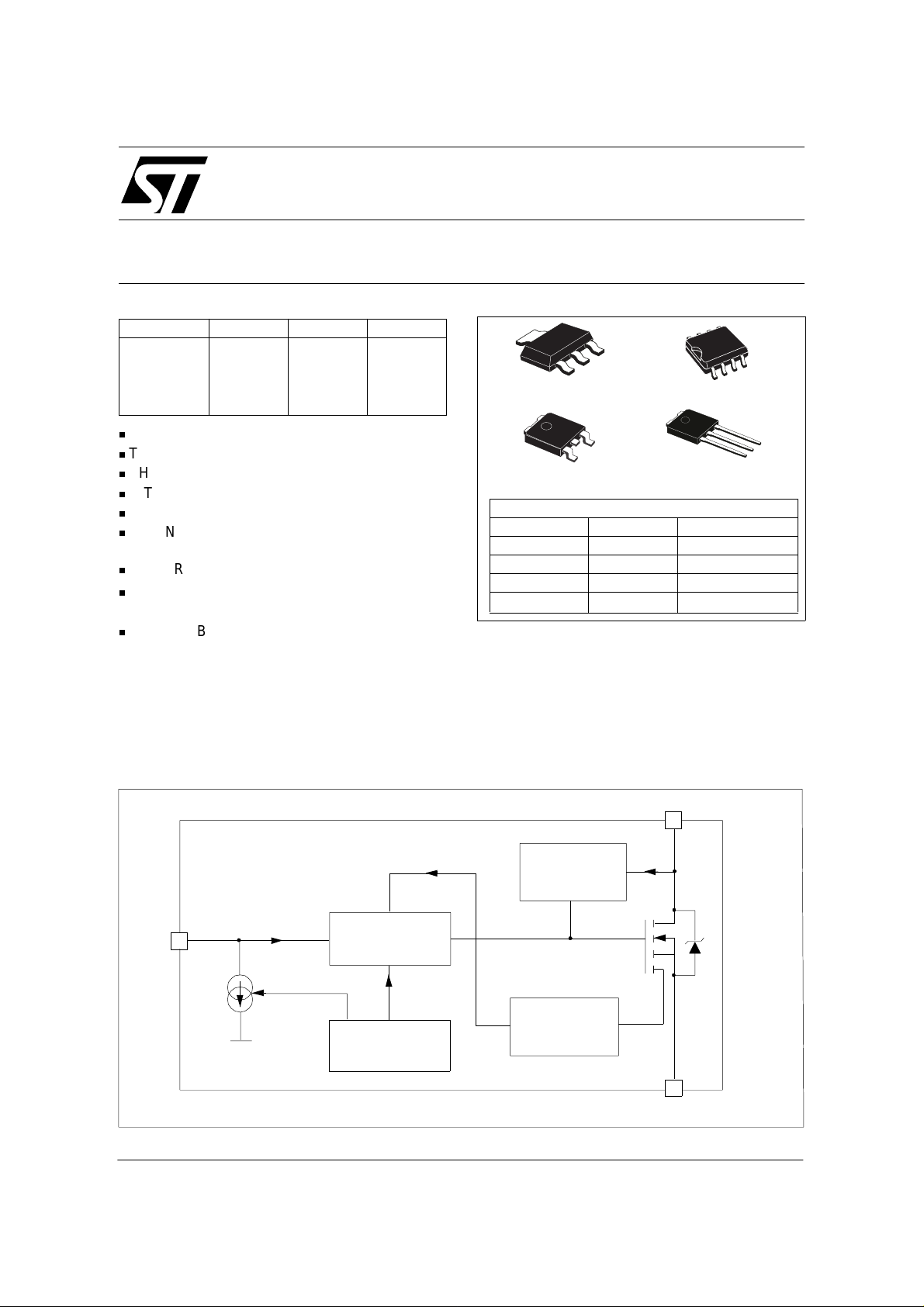
DESCRIPTION
The VNN7NV04, VNS7NV04, VND7NV04
VND7NV04-1, are mon ol ithi c devic es desi g ned in
STMicroelectronics VIPower M0-3 Technology,
intended for replacement of standard Power
BLOCK DIAGRAM
2
3
2
1
SOT-223
3
1
TO25 2 (D PAK)
SO-8
TO251 (IPAK)
3
2
1
ORDER CODES
PACKAGE TUBE T&R
SOT-223 VNN7NV04 VNN7NV0413TR
SO-8 VNS7NV04 VNS7NV0413TR
TO-252 (DPAK) VND7NV04 VND7NV0413TR
TO-251 (IP AK) VND7NV04-1
-
MOSFETS from DC up to 50KHz applications.
Built in thermal shutdown, l inear curren t limitation
and overvoltage cla mp protects the chip in harsh
environments.
Fault feedback can be de tected by mon itori ng the
voltage at the input pin.
DRAIN
2
Overvoltage
Clamp
INPUT
1
Februa ry 2003 1/29
Gate
Control
Over
T emperature
Linear
Current
Limiter
3
SOURCE
FC01000
1
Page 2
VNN7NV04 / VNS7NV04 / VND7NV04 / VND7NV04-1
ABSOLUTE MAXIMUM RATI NG
Symbol Parameter
Drain-source Voltage (VIN=0V) Intern ally Clamped V
Input Voltage Internally Clamped V
IN
Input Current +/-20 mA
Minimum I nput Series Impedance 150 Ω
Drain Current Internally Limited A
Reverse DC Output Current -10.5 A
Electros tatic Discharge (R=1.5KΩ, C=100pF) 4000 V
Electros tatic Discharge on output pin only
(R=330Ω, C=150pF)
Total Dissipation at Tc=25°C 7 4.6 60 W
tot
Maximum Switching Energy (L=0.7mH;
RL=0Ω; V
=13.5V; T
bat
=150ºC; IL=9A)
jstart
Maximum Switching Energy (L=0.6mH;
RL=0Ω; V
Operating Junction Temperature Internally limited °C
j
Case Operating Temperature Internally limit ed °C
c
=13.5V; T
bat
=150ºC; IL=9A)
jstart
Storage Temperatu re -55 to 150 °C
R
V
V
E
E
V
DS
V
I
IN
IN MIN
I
D
I
R
ESD1
ESD2
P
MAX
MAX
T
T
T
stg
CONNECTION DIAGRAM (TO P VI EW)
SOT-223 SO-8 DPAK/IPAK
Value
Unit
16500 V
40 40 mJ
37 mJ
SOURCE
SOURCE
SOURCE
INPUT
1
4
SO-8 Package (*)
(*) For the pins configuration related to SOT-223, DPAK, IPAK see outlines at page 1.
CURRENT AND VOLTAGE CONVEN TIO NS
R
I
IN
V
IN
IN
INPUT
8
5
DRAIN
SOURCE
DRAIN
DRAIN
DRAIN
DRAIN
I
D
V
DS
2/29
1
Page 3
VNN7NV04 / VNS7NV04 / VND7NV04 / VND7NV04-1
THERMAL DATA
Symbol Parameter
R
thj-case
R
thj-lead
R
thj-amb
(*) When mounted on a standard single-sided FR4 board with 0.5cm
Thermal R esistance Junction-case}} } MAX 18 2.1 2.1 °C/W
Thermal R esistance Junction-lead MAX 27 °C/W
Ther ma l R esistan ce J u nction-ambient MAX 96 (*) 90 (*) 65 (*) 102 °C/W
SOT-223 SO-8 DPAK IPAK
2
of Cu (at least 35 µm thick) connected to all DRAIN pins.
ELECTRICAL CHARACTERISTICS (-40°C < Tj < 150°C, unless otherwise specified)
OFF
Symbol Parameter Test Conditions Min Typ Max Unit
V
CLAMP
V
CLTH
V
INTH
I
ISS
V
INCL
I
DSS
Drain-source Clamp
Voltage
Drain-source Clamp
Threshold Voltage
Input Thre shold Voltage VDS=VIN; ID=1mA 0. 5 2.5 V
Supply Current from Input
Pin
Input-Source Clamp
Voltage
Zero Input Voltage Drain
Current (VIN=0V)
VIN=0V; ID=3.5A 40 45 55 V
VIN=0V; ID=2mA 36 V
=0V; VIN=5V 100 150 µA
V
DS
I
=1mA
IN
I
=-1mA
IN
V
=13V; VIN=0V; Tj=25°C
DS
V
=25V; VIN=0V
DS
Value
6
-1.0
6.8 8
-0.3
30
75
Unit
V
µA
ON
Symbol Parameter Test Conditions Min Typ Max Unit
V
R
DS(on)
Static Drain-source On
Resistance
=5V; ID=3.5A; Tj=25°C
IN
V
=5V; ID=3.5A
IN
60
120
mΩ
3/29
1
Page 4
VNN7NV04 / VNS7NV04 / VND7NV04 / VND7NV04-1
ELECTRICAL CHARACTERISTICS (continued) (Tj=25°C, unless otherwise specified)
DYNAMIC
Symbol Parameter Test Conditions Min Typ Max Unit
gfs (*)
C
OSS
SWITCHING
Symbol Parameter Test Conditi ons Min Typ Max Unit
t
d(on)
t
t
d(off)
t
t
d(on)
t
t
d(off)
t
(dI/dt)
Q
Forward
Transconductanc e
VDD=13V; ID=3.5A 9 S
Output Capacitance VDS=13V; f=1MHz; VIN=0V 220 pF
Turn-on Delay Time
Rise Time 470 1500 ns
r
Turn-off Delay Time 500 1500 ns
Fall Time 350 1000 ns
f
Turn-on Delay Time
Rise Time 4.6 14.0 µs
r
Turn-off Delay Time 5.4 16.0 µs
Fall Time 3.6 11.0 µs
f
Turn-on Current Slope
on
Total Input Charge
i
=15V; ID=3.5A
V
DD
V
=5V; R
gen
gen=RIN MIN
(see figure 1)
=15V; ID=3.5A
V
DD
V
gen
=5V; R
gen
=2.2K Ω
(see figure 1)
=15V; ID=3.5A
V
DD
V
=5V; R
V
I
gen
DD
gen
gen=RIN MIN
=12V; ID=3.5A; VIN=5V
=2.13m A (see figure 5)
=150Ω
=150Ω
100 300 ns
0.75 2.3 µs
6.5 A/µs
18 nC
SOURCE DRAIN DIODE
Symbol Parameter Test Conditions M in Typ Max Uni t
(*) Forward On Voltage ISD=3.5A; VIN=0V 0.8 V
V
SD
Q
I
RRM
t
Reverse Recovery Time ISD=3.5A; dI/dt=20A/µs
rr
Reverse Recovery Charge 0.28 µC
rr
Reverse Recovery Current 2.5 A
V
=30V; L= 20 0 µ H
DD
(see test circuit, figure 2)
220 ns
PROTECTIONS (-40°C < Tj < 150°C, unless otherwise specified)
Symbol Parameter Test Conditions M in Typ Max Uni t
I
lim
t
dlim
T
T
I
E
(*) Pulsed: Pu ls e duration = 300µs, duty c y c le 1.5%
Drain Current Limit VIN=5V; VDS=13V 6 9 12 A
=5V; VDS=13V
Step Response Current
Limit
Overtemperature
jsh
Shutdown
Overtemperature Reset 135 °C
jrs
Fault Sink Current VIN= 5V; VDS=13V; Tj=T
gf
Sing l e Pu lse
as
Avala nche Energy
V
IN
starti ng T
V
IN
=25°C; VDD=24V
j
=5V; R
gen=RIN MIN
(see figures 3 & 4)
jsh
=150Ω; L=24mH
4.0 µs
150 175 200 °C
15 mA
200 mJ
4/29
2
Page 5

VNN7NV04 / VNS7NV04 / VND7NV04 / VND7NV04-1
PROTECTION FEATURES
During normal operation, the INPUT pin is
electrically connected to the gate of the internal
power MOSFET through a low impedance path.
The device then behaves like a standard power
MOSFET and can be used as a switch from DC to
50KHz. The only difference from the user’s
standpoint is that a small DC current I
100µA) flows into the INPUT pin in order to supply
ISS
(typ.
the internal circuitry.
The de vice integrates:
- OVERVOLTAGE CLAMP PROTECTION:
internally set at 45V, along with the rugged
avalanche characteristics o f the Power MOSFET
stage giv e this device unrivall ed ruggedne ss and
energy handl ing capability. This feat ure is mainly
important when driving inductive loads.
- LINEAR CURRENT LIMITER CIRCUIT: limits
the drain current ID to I
voltage. When the current limiter is active, the
whatever the INPUT pin
lim
device operates in the linear region, so power
dissipation may exceed the capability of the
heatsink. Both case and junction temperatures
increase, and if this phase lasts long enough,
junction temperature may reach the
overtemperature threshold T
jsh
.
- OVERTEMPERATURE AND SHORT CIRCUI T
PROTECTION: these are based on sensing the
chip temperature and are not dependent on the
input voltage. The location of the sensi ng eleme nt
on the chip in the power st age ar ea ensures f ast,
accurate detection of the junction temperature.
Overtemperatur e cut-out occurs i n the range 1 50
to 190 °C, a typical value being 170 °C. The device
is automatically restarted when the chip
temperature fa lls of about 15°C be low shut-d own
temperature.
- STATUS FEEDBACK: in the case of an
overtemperature fault condition (Tj > T
device tries to sink a diagnostic current Igf thro ug h
jsh
), the
the INPUT pin in order to indicate fault condition. If
driven from a l ow impedance sou rce, this curre nt
may be used in orde r to warn the contr ol circ uit of
a device shut down. If the drive impeda nc e is h i gh
enough so that the INPUT pin dri ver is not abl e to
supply the current Igf, the INPUT pin will fall to 0V.
This will not however affect the device
operation: no requirement is put on the current
capability of t he IN PUT pin dr ive r e xcep t t o b e
able to supply the normal operation drive
current I
ISS
.
Additional features of this device are ESD
protection according to the Human Body model
and the ability to be driven from a TTL Logic
circuit.
5/29
1
Page 6
VNN7NV04 / VNS7NV04 / VND7NV04 / VND7NV04-1
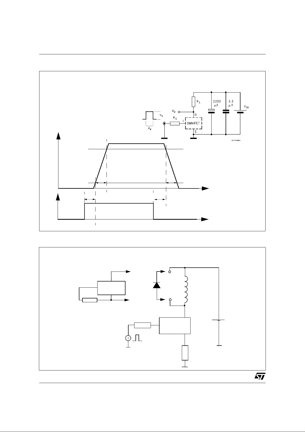
Figure 1: Switching Time Test Circuit for Resistive Load
V
gen
I
D
90%
V
D
R
gen
t
r
t
V
gen
d(on) t
10%
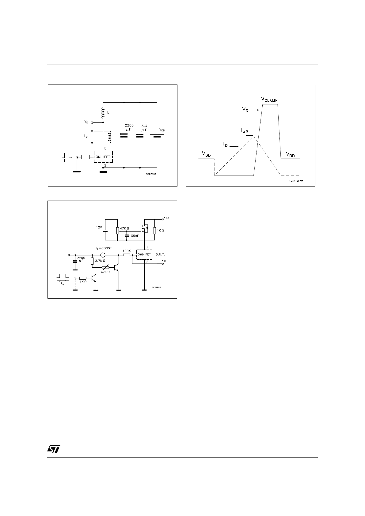
Figure 2: Test Circuit for Diode Recovery Times
A
D
I
OMNIFET
S
150Ω
B
R
gen
FAST
DIODE
d(off)
I
t
f
A
B
OMNIFET
L=100uH
D
t
t
V
DD
6/29
1
V
gen
S
8.5 Ω
Page 7
VNN7NV04 / VNS7NV04 / VND7NV04 / VND7NV04-1
Figure 3: Unclamped Inductive Load Test Circuits
R
V
IN
P
GEN
W
Figur e 5: Input Charge Test Circuit
V
IN
Figure 4: Unclamped Inductive Waveforms
7/29
1
Page 8
VNN7NV04 / VNS7NV04 / VND7NV04 / VND7NV04-1
Source-Drain Diode Forward Characteristics
Vsd (mV)
1000
950
900
850
800
750
700
650
600
550
500
Vin=0V
0 2 4 6 8 101214
Id(A)
Derating Curve
Static Drain-Source On resistance Vs. Input
Voltage
Rds(on) (mOhm)
140
120
Tj=150ºC
100
80
Tj=25ºC
60
Tj=-40ºC
40
20
0
3 3.5 4 4.5 5 5.5 6 6.5
Vin(V)
Id=6A
Id=1A
Id=6A
Id=1A
Id=6A
Id=1A
Static Drain Source On Resistance
Rds(on) (mOhm)
500
450
400
350
300
250
200
150
100
50
0
0 0.25 0.5 0.75 1 1.25
Tj= - 40ºC
Vin=2.5V
Tj=25ºC
Tj=150ºC
Id(A)
Static Drain-Source On resistance Vs. Input
Voltage
Rds(on) (mOhm)
120
110
100
90
80
70
60
50
40
30
20
10
0
33.544.555.566.57
Id=3.5A
Tj=150ºC
Tj=25ºC
Tj= - 40ºC
Vin(V)
Transconductance
Gfs (S)
20
18
16
14
12
10
8
6
4
2
0
Vds=13V
Tj=-40ºC
Tj=25ºC
Tj=150ºC
012345678
Id(A)
8/29
1
1
Page 9
VNN7NV04 / VNS7NV04 / VND7NV04 / VND7NV04-1
Static Drain-Source On Resistance Vs. Id
Rds(on) (mOhm)
140
120
100
80
60
40
20
0
00.511.522.533.544.555.56
Tj=150ºC
Tj=25ºC
Tj=-40ºC
Vin=3.5V
Vin=5V
Vin=3.5V
Vin=5V
Vin=3.5V
Vin=5V
Id(A)
Turn On Current Slope
di/dt(A/us)
8
7
6
5
4
3
2
1
0
100
200
300
400
500
Rg(ohm)
600
Vin=5V
Vdd=15V
Id=3.5A
700
800
900
1000
1100
Transfer Characteristics
Idon(A)
10
9
8
7
6
5
4
3
2
0
Vds=13.5V
1
1 1.5 2 2.5 3 3.5 4 4.5 5 5.5
Vin(V)
Turn On Current Slope
di/dt(A/us)
2.25
2
1.75
1.5
1.25
1
0.75
0.5
0.25
100 200 300 400 500 600 700 800 900 1000 1100
Rg(ohm)
Vin=3.5V
Vdd=15V
Id=3.5A
Tj=25ºC
Tj=-40ºC
Tj=150ºC
Input Voltage Vs. Input Charge
Vin(V)
8
7
6
5
4
3
2
1
0
0 5 10 15 20 25
Vds=12V
Id=3.5A
Qg(nC)
1
Turn off drain source voltage slope
dv/dt(V/us)
300
250
200
150
100
50
0
100 200 300 400 500 600 700 800 900 1000 1100
Rg(ohm)
Vin=5V
Vdd=15V
Id=3.5A
9/29
Page 10

VNN7NV04 / VNS7NV04 / VND7NV04 / VND7NV04-1
Turn Off Drain-Source Voltage Slope
dv/dt(v/us)
300
250
700
Vin=3.5V
Vdd=15V
Id=3.5A
800
900
200
150
100
50
0
100
200
300
400
500
600
Rg(ohm)
Switching Time Resistive Load
t(us)
5.5
5
4.5
3.5
2.5
1.5
0.5
Vdd=15V
Id=3.5A
Vin=5V
4
3
2
1
0
250
0
500
750
1000
1250
td(off)
td(on)
1500
1750
2000
Rg(ohm)
Output Characteristics
1000
2250
Capacitance Variations
C(pF)
600
1100
500
400
300
200
100
0 5 10 15 20 25 30 35
f=1MHz
Vin=0V
Vds(V)
Switching Time Resistive Load
t(ns)
1600
tr
tr
tf
2500
1400
1200
1000
800
600
400
200
0
3.25 3.5 3.75 4 4.25 4.5 4.75 5 5.25
td(off)
td(on)
Vdd=15V
Id=3.5A
Rg=150ohm
tf
Vin(V)
Normalized On Resistance Vs. Temperature
ID(A)
12
11
10
9
8
7
6
5
4
3
2
1
0
012345678910111213
VDS(V)
10/29
1
Vin=5V
Vin=4.5V
Vin=4V
Vin=3V
Vin=2.5V
Vin=2V
Rds(on)
2.25
2
1.75
1.5
1.25
1
0.75
0.5
Vin=5V
Id=3.5A
-50 -25 0 25 50 75 100 125 150 175
T(ºC)
1
Page 11

VNN7NV04 / VNS7NV04 / VND7NV04 / VND7NV04-1
Normalized Input Threshold Voltage Vs.
Temperature
Vin(th)
1.15
1.1
1.05
1
0.95
0.9
0.85
0.8
0.75
0.7
-50 -25 0 25 50 75 100 125 150 175
T(ºC)
Vds=Vin
Id=1mA
Step Response Current Limit
Tdlim(us)
7
6.5
6
Vin=5V
Rg=150ohm
Current Limit Vs. Junction Temperature
Ilim (A)
15
14
13
12
11
10
9
8
7
6
5
Vds=13V
Vin=5V
-50 -25 0 25 50 75 100 125 150 175
Tj (ºC)
5.5
5
4.5
4
3.5
5 101520253035
Vdd(V)
11/29
1
11
Page 12

VNN7NV04 / VNS7NV04 / VND7NV04 / VND7NV04-1
SO-8 Maximum turn off current versus load inductance
LMAX (A)
I
100
10
A
B
C
1
0.01 0.1 1 10 100
A = Single Pulse at T
B= Repetitive pulse at T
C= Repetitive Pulse at T
Conditions:
VCC=13.5V
Values are generated with RL=0Ω
In case of repetitive pulses, T
the temperature specified above for curves B and C.
VIN, I
L
=150ºC
Jstart
=100ºC
Jstart
=125ºC
Jstart
jstart
Demagnetization
(at beginning of each demagnetization) of every pulse must not exceed
L(mH)
Demagnetization
Demagnetization
12/29
t
Page 13

VNN7NV04 / VNS7NV04 / VND7NV04 / VND7NV04-1
DPAK Maximum turn off current versus load inductance
LMAX (A)
I
100
10
A
B
C
1
0.01 0.1 1 10 100
A = Single Pulse at T
B= Repetitive pulse at T
C= Repetitive Pulse at T
Conditions:
VCC=13.5V
Values are generated with RL=0Ω
In case of repetitive pulses, T
the temperature specified above for curves B and C.
VIN, I
L
=150ºC
Jstart
=100ºC
Jstart
=125ºC
Jstart
jstart
Demagnetization
(at beginning of each demagnetization) of every pulse must not exceed
L(mH)
Demagnetization
Demagnetization
t
13/29
Page 14

VNN7NV04 / VNS7NV04 / VND7NV04 / VND7NV04-1
SOT-223 Maximum turn off current versus load inductance
LMAX (A)
I
100
10
A
B
C
1
0.01 0.1 1 10
A = Single Pulse at T
B= Repetitive pulse at T
C= Repetitive Pulse at T
Conditions:
VCC=13.5V
Values are generated with RL=0Ω
In case of repetitive pulses, T
the temperature specified above for curves B and C.
VIN, I
L
=150ºC
Jstart
=100ºC
Jstart
=125ºC
Jstart
jstart
Demagnetization
(at beginning of each demagnetization) of every pulse must not exceed
L(mH)
Demagnetization
Demagnetization
14/29
t
Page 15

SO-8 PC Board
VNN7NV04 / VNS7NV04 / VND7NV04 / VND7NV04-1
SO-8 THERMAL DATA
R
thj-amb
Layout condition of Rth and Zth measurements (PCB FR4 area= 58mm x 5 8m m , PCB thickness=2mm,
Cu thickness=35µm, Copper areas: 0.14cm
Vs PCB copper area in open box free air condition
2
, 0.6cm2, 1.6cm2).
SO-8 at 4 pins connected to TAB
RTHj_amb
(ºC/W)
110
105
100
95
90
85
80
75
70
00.511.522.5
PCB CU heatsink are a (cm^2)
15/29
Page 16

VNN7NV04 / VNS7NV04 / VND7NV04 / VND7NV04-1
SOT-223 THERMAL DATA
SOT-223 PC Board
R
thj-amb
Layout condition of Rth and Zth measurements (PCB FR4 area= 58mm x 5 8m m , PCB thickness=2mm,
Cu thickness=35µm, Copper areas: 0.11cm
2
, 1cm2, 2cm2).
Vs PCB copper area in open box free air condition
RTH j-amb (°C/W)
140
130
120
110
100
90
80
16/29
70
60
00.511.522.5
Cu area (cm^2)
Page 17

DPAK PC Board
VNN7NV04 / VNS7NV04 / VND7NV04 / VND7NV04-1
DPAK THERMAL DATA
Layout condition of Rth and Zth measur em ents (PCB FR 4 area= 60mm x 60mm, PCB thickness=2mm,
Cu thickness=35µm, Copper areas: from mi nimum pad lay-out to 8c m
R
Vs PCB copper area in open box free air condition
thj-amb
RTH j_amb (ºC/W)
90
80
70
60
50
40
2
).
30
0246810
PCB CU heatsink area (cm^2)
17/29
Page 18

VNN7NV04 / VNS7NV04 / VND7NV04 / VND7NV04-1
DPAK Thermal Impedance Junction Ambient Single Pulse
ZTH (°C/W)
1000
100
10
1
0.1
0.0001 0.001 0.01 0.1 1 10 100 1000
Time (s)
Thermal fitting model of an OMNIFET II in
DPAK
Tj
C1
R1 R2
Pd
C2
C3
R3
T_amb
C4
R4
C5
R5
C6
R6
Pulse calculation formula
Z
THδ
where
RTHδ Z
δ tpT⁄=
THtp
Thermal Paramet er
Area/island (cm2) Footpri nt 6
R1 (°C/W) 0.1
R2 (°C/W) 0.35
R3 ( °C/W) 1.20
R4 (°C/W) 2
R5 (°C/W) 15
R6 (°C/W) 61 24
C1 (W.s/°C) 0.0006
C2 (W.s/°C) 0.0021
C3 (W.s/°C) 0.05
C4 (W.s/°C) 0.3
C5 (W.s/°C) 0.45
C6 (W.s/°C) 0.8 5
Footprint
2
6 cm
1 δ–()+⋅=
18/29
Page 19

VNN7NV04 / VNS7NV04 / VND7NV04 / VND7NV04-1
SO-8 Thermal Impedance Junction Ambient Single Pulse
ZTH (°C/W)
1000
100
10
1
0.1
0.0001 0.001 0.01 0.1 1 10 100 1000
Time (s)
Thermal fitting model of an OMNIFET II in SO-8
Tj
C1
R1 R2
Pd
C2
C3
R3
T_amb
C4
R4
C5
R5
C6
R6
Pulse calculation formula
Z
THδ
where
RTHδ Z
δ tpT⁄=
THtp
Thermal Paramet er
Area/island (cm2) Footpri nt 2
R1 (°C/W) 0.2
R2 (°C/W) 0.9
R3 ( °C/W) 3.5
R4 (°C/W) 21
R5 (°C/W) 16
R6 (°C/W) 58 28
C1 (W.s/°C) 3.00E-04
C2 (W.s/°C) 9.00E-04
C3 (W.s/°C) 7.50E-03
C4 (W.s/°C) 0.045
C5 (W.s/°C) 0.35
C6 (W.s/°C) 1.05 2
Footprint
2
2 cm
1 δ–()+⋅=
19/29
Page 20

VNN7NV04 / VNS7NV04 / VND7NV04 / VND7NV04-1
SOT-223 Thermal Impedance Junction Ambient Single Pulse
ZTH (°C/W)
1000
100
10
1
0.1
Footprint
2
2 cm
0.0001 0.001 0.01 0.1 1 10 100 1000
Time (s)
Thermal fitting model of an OMNIFET II in
SOT-223
Tj
C1
R1 R2
Pd
C2
C3
R3
T_amb
C4
R4
C5
R5
C6
R6
Pulse calculation formula
Z
THδ
where
RTHδ Z
δ tpT⁄=
THtp
Thermal Paramet er
Area/island (cm2) Footpri nt 2
R1 (°C/W) 0.2
R2 (°C/W) 1.1
R3 ( °C/W) 4.5
R4 (°C/W) 24
R5 (°C/W) 0.1
R6 (°C/W) 100 45
C1 (W.s/°C) 3.00E-04
C2 (W.s/°C) 9.00E-04
C3 (W.s/°C) 3.00E-02
C4 (W.s/°C) 0.16
C5 (W.s/°C) 1000
C6 (W.s/°C) 0.5 2
1 δ–()+⋅=
20/29
Page 21

VNN7NV04 / VNS7NV04 / VND7NV04 / VND7NV04-1
TO-251 (IPAK) MECHANICAL DATA
DIM.
MIN. TYP MAX. MIN. TYP. MAX.
mm. inch
A 2.2 2.4 0.086 0.094
A1 0.9 1.1 0.035 0.043
A3 0.7 1.3 0.027 0.051
B 0.64 0.9 0.025 0.031
B2 5.2 5.4 0.204 0.212
B3 0.85 0.033
B5 0.3 0.012
B6 0.95 0.037
C 0.45 0.6 0.017 0.023
C2 0.48 0.6 0.019 0.023
D 6 6.2 0.236 0.244
E 6.4 6.6 0.252 0.260
G 4.4 4.6 0.173 0.181
H 15.9 16.3 0.626 0.641
L 9 9.4 0.354 0.370
L1 0.8 1.2 0.031 0.047
L2 0.8 1 0.031 0.039
H
A
E
= =
C2
L2
B2
= =
C
A3
A1
B6
L
B
B5
G
= =
D
B3
2
1 3
L1
21/29
1
1
1
Page 22

VNN7NV04 / VNS7NV04 / VND7NV04 / VND7NV04-1
TO-252 (DPAK) MECHANICAL DATA
DIM.
mm. inch
MIN. TYP MAX. MIN. TYP. MAX.
A 2.2 2.4 0.086 0.094
A1 0.9 1.1 0.035 0.043
A2 0.03 0.23 0.001 0.009
B 0.64 0.9 0.025 0.035
B2 5.2 5.4 0.204 0.212
C 0.45 0.6 0.017 0.023
C2 0.48 0.6 0.019 0.023
D 6 6.2 0.236 0.244
E 6.4 6.6 0.252 0.260
G 4.4 4.6 0.173 0.181
H 9.35 10.1 0.368 0.397
L2 0.8 0.031
L4 0.6 1 0.023 0.039
R 0.2 0.008
V2 0° 8° 0° 8°
22/29
D
R
A
C2
A1
L2
B
=
E
B2
===
L4
H
C
V2
A2
==
==
G
0.60 MIN.
FLAT ZONE
Page 23

VNN7NV04 / VNS7NV04 / VND7NV04 / VND7NV04-1
SOT-223 MECHANICAL DATA
DIM.
MIN. TYP MAX. MIN. TYP. MAX.
A 1.8 0.071
B 0.6 0.7 0.85 0.024 0.027 0.033
B1 2.9 3 3.15 0.114 0.118 0.124
c 0.24 0.26 0.35 0.009 0.01 0.014
D 6.3 6.5 6.7 0.248 0.256 0.264
e2.3 0.09
e1 4.6 0.181
E 3.3 3.5 3.7 0.13 0.138 0.146
H 6.7 7 7.3 0.264 0.276 0.287
V10 (max)
A1 0.02 0.1 0.0008 0.004
mm. inch
0046067
23/29
Page 24

VNN7NV04 / VNS7NV04 / VND7NV04 / VND7NV04-1
SO-8 MECHANICAL DATA
DIM.
MIN. TYP MAX. MIN. TYP. MAX.
A 1.75 0.068
a1 0.1 0.25 0.003 0.009
a2 1.65 0.064
a3 0.65 0.85 0.025 0.033
b 0.35 0.48 0.013 0.018
b1 0.19 0.25 0.007 0.010
C 0.25 0.5 0.010 0.019
c1 45 (typ.)
D 4.8 5.0 0.188 0.196
E 5.8 6.2 0.228 0.244
e 1.27 0.050
e3 3.81 0.150
F 3.8 4.0 0.14 0.157
L 0.4 1.27 0.015 0.050
M 0.6 0.023
F 8 (max.)
mm. inch
24/29
1
Page 25

SOT-223 TAPE AND REEL SHIPMENT (suffix “13TR”)
TAPE DIMENSIONS
According to Electr onic Industries Association
(EIA) Sta ndard 481 rev. A, Feb. 1986
Tape width W 12
Tape Hole Spacing P0 (± 0.1) 4
Component Spacing P 8
Hole Diameter D (± 0.1/-0) 1.5
Hole Diameter D1 (min) 1.5
Hole Position F (± 0.05) 5.5
Compartment Depth K (max) 4.5
Hole Spacing P1 (± 0.1) 2
VNN7NV04 / VNS7NV04 / VND7NV04 / VND7NV04-1
REEL DIMENS I O N S
Base Q.ty 1000
Bulk Q.ty 1000
A (max) 330
B (min) 1.5
C (± 0.2) 13
F 20.2
G (+ 2 / -0) 12.4
N (min) 60
T (max) 18.4
All dimensions are i n mm.
Top
cover
tape
End
500mm min
Empty components pockets
saled with cover tape.
User direction of feed
Start
No componentsNo components Components
500mm min
25/29
1
Page 26

VNN7NV04 / VNS7NV04 / VND7NV04 / VND7NV04-1
SO-8 TUBE SHIPMENT (no suffix)
B
C
Base Q.ty 100
Bulk Q.ty 2000
Tube length (± 0.5) 532
A
A 3.2
B 6
C (± 0.1) 0.6
All dimensions are i n mm.
TAPE AND REEL SHIPMENT (suffix “13TR”)
REEL DIMENSIONS
Base Q.ty 2500
Bulk Q.ty 2500
A (max) 330
B (min) 1.5
C (± 0.2) 13
F 20.2
G (+ 2 / -0) 12.4
N (min) 60
T (max) 18.4
All dimensions are in mm.
TAPE DIMENSIONS
According to Electr onic Industries Association
(EIA) S tanda rd 481 rev. A, Feb 1986
Tape width W 12
Tape Hole Spacing P0 (± 0.1) 4
Component Spacing P 8
Hole Diameter D (± 0.1/-0) 1.5
Hole Diameter D1 (min) 1.5
Hole Position F (± 0.05) 5.5
Compartment Depth K (max) 4.5
Hole Spacing P1 (± 0.1) 2
All dimensions are i n mm.
26/29
Top
cover
tape
End
500mm min
Empty components pockets
saled with cover tape.
User direction of feed
Start
No componentsNo components Components
500mm min
1
Page 27

VNN7NV04 / VNS7NV04 / VND7NV04 / VND7NV04-1
DPAK FOOTPRINT TUBE SHIPMENT (no suffix)
6.7
6.7 3.01.8 1.6
2.3
2.3
TAPE AND REEL SHIPMENT (suffix “13TR”)
A
Base Q.ty 75
C
Bulk Q.ty 3000
Tube length (± 0. 5) 532
A 6
B
B 21.3
C (± 0.1) 0.6
All dimensions are in mm.
REEL DIMENSIONS
Base Q.ty 2500
Bulk Q.ty 2500
A (max) 330
B (min) 1.5
C (± 0.2) 13
F 20.2
G (+ 2 / -0) 16.4
N (min) 60
T (max) 22.4
TAPE DIMENSIONS
According to Electronic Industries Association
(EIA) Standard 481 rev. A, Feb 1986
Tape width W 16
Tape Hole Spacing P0 (± 0.1) 4
Component Spacing P 8
Hole Diameter D (± 0.1/-0) 1.5
Hole Diameter D1 (min) 1.5
Hole Position F (± 0.05) 7.5
Compartm ent Depth K (max) 6.5
Hole Spacing P1 (± 0.1) 2
All dimensions are in mm.
Top
cover
tape
End
500mm min
Empty components pockets
saled with cover tape.
User direction of feed
Start
No componentsNo components Components
500mm min
27/29
1
Page 28

VNN7NV04 / VNS7NV04 / VND7NV04 / VND7NV04-1
IPAK TUBE SHIP MENT (no suffix)
A
C
Base Q.ty 75
Bulk Q.ty 3000
Tube length (± 0.5) 532
B
A 6
B 21.3
C (± 0.1) 0.6
All dimensions are in mm.
28/29
1
Page 29

VNN7NV04 / VNS7NV04 / VND7NV04 / VND7NV04-1
Information furnish ed is believed to be accurate and r eliable. However, STMicroel ec tronics ass um es no responsibility for the consequences
of use of such information nor for any infringement of patents or other rights of third parties which may results from its use. No license is
granted by implication or otherwise unde r any patent or patent rights of STMicroelect r onics. Specifications mentioned in this publication are
subject to c hange without notice. T his publication supersedes and replac es all information pr ev iously supplied. STMicroelectr on ics products
are not authorized for use as critical components in life support devices or systems without express written approval of STMicroelectronics.
Australia - Brazil - Canada - Ch ina - Finland - Franc e - Germany - Ho ng K ong - India - Israel - Italy - J apan - Malaysia -
Malta - Morocco - Singapore - Spain - Sweden - Switzerland - United Kingdom - U.S.A.
The ST logo is a trademark of STMicroele c tronics
2003 STMicroelectronics - Printed in ITALY- All Rights Reserved.
STMicroelectronics GROUP OF COMPANIES
http://www.st.com
29/29
 Loading...