

Page 1
VND600SP
DOUBLE CHANNEL HIGH SIDE SOLID STATE RELAY
TARGET SPECIFICATION
TYPE R
DS(on)
VND600SP 30mΩ 25A 36 V
■ DC SHORT CIRCUIT CURRENT: 25 A
■ CMOS COMPATIBLE INPUTS
■ PROPORTIONAL LOAD CURRENT SENSE
■ UNDERVOLTAGE AND OVERVOLTAGEn
SHUT-DOWN
■ OVERVOLTAGE CLAMP
■ THERMAL SHUT DOWN
■ CURRENT LIMITATION
■ VERY LOW STAND-BY POWER DISSIPATION
■ PROTECTION AGAINST:
n LOSS OF GROUND ANDLOSS OF V
■ REVERSE BATTERY PROTECTION (*)
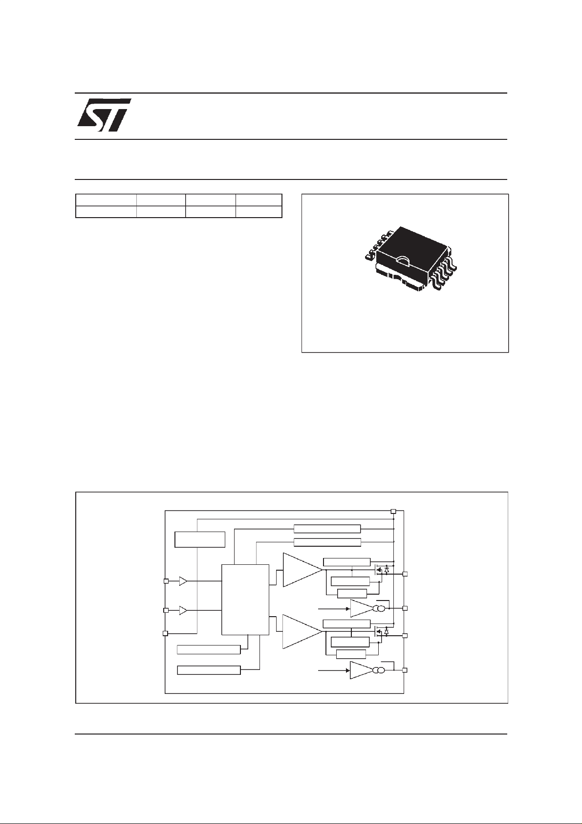
DESCRIPTION
The VND600SP is a monolithic device made
using STMicroelectronics VIPower technology. It
is intended for driving resistive or inductive loads
with one side connectedtoground.ActiveV
voltage clamp protects the device against low
energy spikes (see ISO7637 transient
BLOCK DIAGRAM
I
lim
V
CC
10
1
PowerSO-10
CC
compatibility table). This device has two channels
in high side configuration; each channel has an
analog sense output on which the sensing current
is proportional (according to a known ratio) to the
corresponding load current. Built-in thermal shutdown and outputs current limitation protect the
chip from over temperature and short circuit.
Device turns off in case of ground pin
CC
pin
disconnection.
V
CC
OVERVOLTAGE
VCCCLAMP
INPUT 1
INPUT 2
GND
OVERTEMP.1
OVERTEMP. 2
(*) See application schematic at page7
LOGIC
Ot1
Ot2
UNDERVOLTAGE
DRIVER 1
I
OUT1
DRIVER2
I
OUT2
PwCLAMP 1
I
LIM1
V
dslim1
K
PwCLAMP 2
I
LIM2
V
dslim2
K
OUTPUT 1
Ot1
CURRENT
SENSE 1
OUTPUT 2
Ot2
CURRENT
SENSE 2
September 1999 1/10
1
Page 2
VND600SP
ABSOLUTE MAXIMUM RATING
Symbol Parameter Value Unit
V
-V
-I
GND
I
OUT
I
I
V
CSENSE
V
ESD
P
TOT
T
T
T
STG
CONNECTION DIAGRAM (TOP VIEW)
DC supply voltage 41 V
CC
Reverse supply voltage -0.3 V
CC
DC reverse ground pin current -200 mA
Output current Internally limited A
Reverse output current -21 A
R
Input current +/- 10 mA
IN
Current sense maximum voltage
-3
+15
Electrostatic discharge (R=1.5kΩ; C=100pF) 2000 V
Power dissipation at Tc=25°C90W
Junction operating temperature Internally limited °C
j
Case operating temperature -40 to 150 °C
c
Storage temperature -55 to 150 °C
V
V
GROUND
INPUT 2
INPUT 1
C.SENSE1
C.SENSE2
10
V
CC
CURRENT ANDVOLTAGE CONVENTIONS
I
IN1
V
IN1
I
IN2
V
IN2
INPUT1
CURRENT SENSE 1
INPUT2
CURRENT SENSE 2
6
7
8
9
11
GROUND
V
CC
OUTPUT1
OUTPUT2
5
4
3
2
1
I
OUT1
I
SENSE1
I
OUT2
I
SENSE2
V
SENSE2
V
V
OUT2
I
CC
SENSE1
OUTPUT 2
OUTPUT 2
N.C.
OUTPUT 1
OUTPUT 1
V
OUT1
V
CC
2/10
1
I
GND
Page 3
VND600SP
THERMAL DATA
Symbol Parameter Value Unit
R
R
Note: (1) one channel ON
ELECTRICAL CHARACTERISTICS (8V<VCC<36V; -40°C<Tj<150°C;unless otherwise specified)
(Per each channel)
POWER
(1) Thermal resistance junction-case (MAX) 1.75 °C/W
thj-case
(2) Thermal resistance junction-case (MAX) 1.2 °C/W
thj-case
R
thj-amb
(2) twochannels ON
Thermal resistance junction-ambient (MAX) 50 °C/W
Symbol Parameter Test Conditions Min Typ Max Unit
V
V
V
R
V
I
CC
USD
OV
ON
clamp
I
S
L(off)
Operating supply
voltage
5.5 13 36 V
Undervoltage shutdown 3 4 5.5 V
Overvoltage shutdown 36 42 48 V
I
OUT
On state resistance
Clamp voltage
I
OUT
I
OUT
=20 mA
I
CC
(see note 1)
Off state; Input n.c.; V
Supply current
On state; V
R
SENSE
Off state output current VIN=V
=5A; Tj=25°C
=5A; Tj=150°C
=3A; VCC=6V
41 48 55 V
=13V
CC
=5V; VCC=13V;I
IN
=3.9kΩ
=0V 0 50 µA
OUT
OUT
=0A;
30
60
100
40
6
mΩ
mΩ
mΩ
µA
mA
SWITCHING (VCC=13V)
Symbol Parameter Test Conditions Min Typ Max Unit
(dV
(dV
t
d(on)
t
d(off)
OUT
OUT
Turn-on delay time R1=2.6Ω 30 µs
Turn-on delay time R1=2.6Ω 30 µs
/dt)onTurn-on voltage slope R1=2.6Ω 0.20 V/µs
/dt)
Turn-off voltage slope R1=2.6Ω 0.20 V/µs
off
PROTECTIONS
Symbol Parameter Test Conditions Min Typ Max Unit
T
T
HYST
V
demag
V
I
lim
TSD
T
ON
=13V
V
DC short circuit current
CC
5.5V<VCC<36V
Thermal shut-down
temperature
Thermal reset
R
temperature
Thermal hysteresis 7 15 °C
=2A; VIN=0V; L=6mH
Turn-off output voltage
I
OUT
clamp
Output voltage drop
limitation
I
=0.5A
OUT
Tj= -40°C...+150°C
25 40 70
70
150 175 200 °C
135 °C
Vcc-41 Vcc-48 Vcc-55 V
50 mV
A
A
3/10
1
Page 4

VND600SP
CURRENT SENSE (9V≤V
≤16V) (See fig. 1)
CC
Symbol Parameter Test Conditions Min Typ Max Unit
K
K
K
V
SENSE1,2
V
SENSEH
I
1
OUT/ISENSE
I
2
OUT/ISENSE
I
3
OUT/ISENSE
Max analog sense
output voltage
Analog sense output
voltage in overtemperature
condition
or I
OUT1
other channels open; Tj= -40°C...150°C
I
or I
OUT1
channels open; Tj=-40°C
Tj=25°C...150°C
I
or I
OUT1
channels open; Tj=-40°C
Tj=25°C...150°C
VCC=5.5V; I
VCC>8V, I
V
=13V; R
CC
OUT2
OUT2
OUT2
OUT1,2
OUT1,2
SENSE
=0.5A; V
=5A; V
=15A; V
=2.5A; R
=5A; R
=3.9kΩ
SENSE
SENSE
SENSE
SENSE
=0.5V;
=4V; other
=4V; other
=10kΩ
SENSE
=10kΩ
3300 4400 6000
4200
4400
4200
4400
4900
4900
4900
4900
6000
5750
5500
5250
2
4
5.5 V
I
LOGIC INPUT (Channels 1,2)
Symbol Parameter Test Conditions Min Typ Max Unit
V
I
V
I
V
I(hyst)
V
Note 1: V
Input low level voltage 1.25 V
IL
Low level input current VIN=1.25V 1 µA
IL
Input high level voltage 3.25 V
IH
High level input current VIN=3.25V 10 µA
IH
Input hysteresis voltage 0.5 V
Input clamp voltage
ICL
and VOVare correlated. Typical difference is 5V.
clamp
I
IN
I
IN
=1mA
=-1mA
6.5 7.4
-0.7
8.5 V
TRUTH TABLE (per channel)
V
V
V
CONDITIONS INPUT OUTPUT SENSE
Normal operation
Overtemperature
Undervoltage
Overvoltage
Short circuit to GND
Short circuit to V
CC
Negative output voltage
clamp
4/10
L
H
L
H
L
H
L
H
L
H
L
H
L
H
L
L
L
L
L
L
L
L
H
H
0
Nominal
0
V
SENSEH
0
0
0
0
0
0
0
< Nominal
LL 0
2
Page 5

ELECTRICAL TRANSIENT REQUIREMENTS
VND600SP
ISO T/R 7637/1
Test Pulse
I II III IV Delays and
1 -25 V -50 V -75 V -100 V 2 ms 10 Ω
2 +25 V +50 V +75 V +100 V 0.2 ms 10 Ω
3a -25 V -50 V -100 V -150 V 0.1 µs50Ω
3b +25 V +50 V +75 V +100 V 0.1 µs50Ω
4 -4 V -5 V -6 V -7 V 100 ms, 0.01 Ω
5 +26.5 V +46.5V +66.5 V +86.5 V 400 ms, 2 Ω
ISO T/R 7637/1
Test Pulse
I II III IV
TEST LEVELS RESULTS
1CCCC
2CCCC
3aCCCC
3bCCCC
4CCCC
5C E E E
CLASS CONTENTS
C All functions of the device are performed as designed after exposure to disturbance.
E
One or more functions of the device is not performed as designed after exposure to disturbance
and cannot be returned to proper operation without replacing the device.
SWITCHING CHARACTERISTICS
TEST LEVELS
Impedance
V
OUT
dV
OUT
INPUT
/dt
(on)
t
d(on)
70%
t
90%
dV
/dt
OUT
(off)
r
10%
t
d(off)
t
f
t
t
5/10
Page 6

VND600SP
Figure1: Waveforms
INPUT
n
LOAD CURRENT
SENSE
n
V
CC
INPUT
n
LOAD CURRENT
SENSE
n
V
CC
INPUT
n
LOAD CURRENT
SENSE
n
NORMAL OPERATION
n
UNDERVOLTAGE
V
USDhyst
V
USD
n
OVERVOLTAGE
V
OV
VCC<V
OV
n
VCC>V
OV
INPUT
n
LOAD CURRENT
LOAD VOLTAGE
SENSE
n
INPUT
n
LOAD VOLTAGE
LOAD CURRENT
SENSE
n
T
j
INPUT
n
LOAD CURRENT
SENSE
n
SHORT TO GROUND
n
n
SHORT TO V
n
n
<Nominal
T
TSD
T
R
n
OVERTEMPERATURE
CC
<Nominal
I
SENSE
=
V
SENSEH
R
SENSE
6/10
Page 7

APPLICATION SCHEMATIC
+5V
R
prot
R
µC
prot
R
prot
INPUT1
CURRENTSENSE1
INPUT2
VND600SP
V
CC
D
ld
OUTPUT1
R
SENSE1
R
prot
CURRENTSENSE2
R
SENSE2
GND PROTECTION NETWORK AGAINST
REVERSE BATTERY
Solution 1: Resistor in the ground line (R
can be used withany type of load.
The following is an indication on how to dimension the
resistor.
R
GND
1) R
2) R
where -I
be found in the absolute max imum r ating s ection of the
≤ 600mV / I
GND
≥ (−VCC) / (-I
GND
is the DC reverse groundpin current and can
GND
S(on)max
)
GND
.
device’s datasheet.
Power Dissipation in R
battery situations) is:
= (-VCC)2/R
P
D
GND
(when VCC<0: during reverse
GND
This r esistor can be shared amongst several different
HSD. Please note that the value of this resistor should be
calculated with formula (1) wher e I
sum of the maximum on-state c urrents of t he different
S(on)max
devices.
Please note that if the m icroprocessor ground i s not
common with the device ground then the R
*R
produce a shift (I
and the status output values. This shift will vary
S(on)max
) in the input thresholds
GND
depending o n how many devices are ON in the case o f
several high side drivers sharing the same R
only). This
GND
becomes the
GND
.
GND
will
GND
R
V
GND
GND
D
OUTPUT2
GND
If thecalculated power dissipation leadsto a large resistor
or several devices have to share the same resistor then
the ST sug gests to utilize Solution 2 (see below).
Solution 2: A diode (D
A resistor ( R
if the device will be drivingan inductive load.
D
GND
=1kΩ) s hould be inserted in para llel to
GND
) in the ground line.
GND
This small signal di ode can be safely shared amongst
several different HSDs. Also in this case, the presence of
the grou nd network will pro duce a shift ( j 600mV) in the
input thresholds and t he s tatus output values if the
microprocessor ground is not common with the de vice
ground. This shift will not vary if more than o ne HSD
shares the same diode/resistor network.
LOAD DUMP PROT ECTION
Dldis necessary (Transil or MOV) if the load dump peak
voltage exceeds V
the devicewill be subject totransients on the V
are greater th an the ones sho wn in the ISO T/R 7637/1
table.
max DC rating. The same applies if
CC
µC I/Os PROTECTION:
If a ground protection netwo rk is used and ne gative
transient are present on the V
be pulled negative. ST suggests toinsert a resistor (R
in line to prevent the µC I/Os pins to latch-up.
The value of these resistors is acompromise between the
leakage current of µC and the current required by the
line, t he control pins w ill
CC
CC
linethat
prot
)
7/10
11
Page 8

VND600SP
HSD I/Os(Input levels compatibility)withthe latch-uplimit
ofµC I/Os.
≤ R
-V
CCpeak/Ilatchup
Fig 1: I
I
OUT/ISENSE
OUT/ISENSE
prot
versus I
≤ (V
OUT
OHµC-VIH
-V
GND
)/I
IHmax
6500
6000
5500
max.Tj=25...150°C
5000
4500
min.Tj=25...150°C
4000
3500
Calculation example:
CCpeak
prot
= - 100V and I
≤ 65kΩ.
prot
For V
5kΩ ≤ R
Recommended R
≥ 20mA; V
latchup
value is 10kΩ.
max.Tj=-40°C
typical value
min.Tj=-40°C
OHµC
≥ 4.5V
3000
0246810121416
I
(A)
OUT
8/10
1
Page 9

PowerSO-10 MECHANICAL DATA
VND600SP
DIM.
MIN. TYP MAX. MIN. TYP. MAX.
mm. inch
A 3.35 3.65 0.132 0.144
A1 0.00 0.10 0.000 0.004
B 0.40 0.60 0.016 0.024
c 0.35 0.55 0.013 0.022
D 9.40 9.60 0.370 0.378
D1 7.40 7.60 0.291 0.300
E 9.30 9.50 0.366 0.374
E1 7.20 7.40 0.283 0.291
E2 7.20 7.60 0.283 300
E3 6.10 6.35 0.240 0.250
E4 5.90 6.10 0.232 0.240
e 1.27 0.050
F 1.25 1.35 0.049 0.053
H 13.80 14.40 0.543 0.567
h 0.50 0.002
Q 1.70 0.067
α 0º 8º
B
==
==
HE
h
A
F
A1
610
51
eB
M
0.25
D
==
D1
==
DETAIL”A”
E2
==
DETAIL”A”
Q
0.10 A
E1E3
==
SEATING
PLANE
A
C
α
B
E4
==
SEATING
PLANE
A1
L
==
9/10
1
Page 10

VND600SP
Information furnished is believed to be accurate and reliable. However,STMicroelectronics assumes no responsibility for the consequences
of use of such information nor for any infringement of patents or other rights of third parties which may results from its use. No license is
granted by implication or otherwise under any patent or patent rights of STMicroelectronics. Specifications mentioned in this publication are
subject tochange without notice. This publication supersedes and replaces all information previously supplied. STMicroelectronics products
are not authorized for use as critical components in life support devices or systems without express written approvalof STMicroelectronics.
Australia - Brazil - Canada- China - France - Germany - Italy - Japan - Korea - Malaysia - Malta - Mexico - Morocco -
The Netherlands - Singapore - Spain - Sweden - Switzerland - Taiwan- Thailand - United Kingdom - U.S.A.
The ST logo is a registered trademarkof STMicroelectronics
1999 STMicroelectronics - Printed in ITALY- All Rights Reserved.
STMicroelectronics GROUPOF COMPANIES
http://www.st.com
10/10
1
 Loading...