

Page 1

INTEGRATED CIRCUITS
DATA SH EET
UDA1361TS
96 kHz sampling 24-bit stereo
audio ADC
Product specification
File under Integrated Circuits, IC01
2001 Jan 17
Page 2
Philips Semiconductors Product specification
96 kHz sampling 24-bit stereo audio ADC UDA1361TS
FEATURES
General
• Low power consumption
• 256, 384, 512 and 768fs system clock
• 2.4 to 3.6 V power supply
• Supports sampling frequency of 5 to 110 kHz
• Small package size (SSOP16)
• Integrated high-pass filter to cancel DC offset
• Power-down mode
• Supports 2 V (RMS) input signals
• Easy application
• Master or slave operation.
Multiple format output interface
• I2S-bus and MSB-justified format compatible
• Up to 24 significant bits serial output.
Advanced audio configuration
GENERAL DESCRIPTION
The UDA1361TS is a single chip stereo Analog-to-Digital
Converter (ADC) employing bitstream conversion
techniques. The low power consumption and low voltage
requirements make the device eminently suitable for use
in low-voltage low-powerportable digital audio equipment
which incorporates recording functions.
TheUDA1361TSsupportstheI2S-busdataformatandthe
MSB-justified data format with word lengths of up to
24 bits.
• Stereo single-ended input configuration
• High linearity, dynamic range and low distortion.
ORDERING INFORMATION
TYPE
NUMBER
UDA1361TS SSOP16 plastic shrink small outline package; 16 leads; body width 4.4 mm SOT369-1
NAME DESCRIPTION VERSION
PACKAGE
2001 Jan 17 2
Page 3
Philips Semiconductors Product specification
96 kHz sampling 24-bit stereo audio ADC UDA1361TS
QUICK REFERENCE DATA
SYMBOL PARAMETER CONDITIONS MIN. TYP. MAX. UNIT
Supplies
V
DDA
V
DDD
I
DDA
I
DDD
T
amb
Analog
V
i(rms)
(THD + N)/S total harmonic
S/N signal-to-noise ratio V
α
cs
analog supply voltage 2.4 3.0 3.6 V
digital supply voltage 2.4 3.0 3.6 V
analog supply current fs= 48 kHz
operating mode − 10.5 − mA
Power-down mode − 0.5 − mA
digital supply current fs= 48 kHz
operating mode − 3.5 − mA
Power-down mode − 0.45 − mA
ambient temperature −40 − +85 °C
input voltage (RMS value) at 0 dB(FS) equivalent − 1.1 − V
at −1 dB(FS) signal output − 1.0 − V
fs= 48 kHz
distortion-plus-noise to signal ratio
at −1dB −−88 −83 dB
at −60 dB; A-weighted −−40 −34 dB
f
= 96 kHz
s
at −1dB −−85 −80 dB
at −60 dB; A-weighted −−40 −37 dB
= 0 V; A-weighted
i
f
= 48 kHz − 100 − dB
s
f
= 96 kHz − 100 − dB
s
channel separation − 100 − dB
2001 Jan 17 3
Page 4
Philips Semiconductors Product specification
96 kHz sampling 24-bit stereo audio ADC UDA1361TS
BLOCK DIAGRAM
handbook, full pagewidth
PINNING
V
INL
V
INR
DATAO
BCK
WS
DDA
V
SSA
16
V
1
3
13
11
12
V
RP
15
DIGITAL
INTERFACE
V
RN
5
ADC
Σ∆
ADC
Σ∆
V
ref
4
2
UDA1361TS
DECIMATION
FILTER
DC-CANCELLATION
FILTER
SYSCLK
8
CLOCK
CONTROL
10
14
MGT451
9
V
DDD
V
SSD
MSSEL
7
PWON
6
SFOR
Fig.1 Block diagram.
SYMBOL PIN DESCRIPTION
V
INL
V
ref
V
INR
V
RN
V
RP
1 left channel input
2 reference voltage
3 right channel input
4 negative reference voltage
5 positive reference voltage
SFOR 6 data format selection input
PWON 7 power control input
SYSCLK 8 system clock 256, 384, 512 or 768f
V
V
DDD
SSD
9 digital supply voltage
10 digital ground
BCK 11 bit clock input/output
WS 12 word select input/output
DATAO 13 data output
MSSEL 14 master/slave select
V
V
SSA
DDA
15 analog ground
16 analog supply voltage
s
handbook, halfpage
V
1
INL
V
2
ref
V
3
INR
V
4
RN
RP
UDA1361TS
5
6
7
8
V
SFOR
PWON
SYSCLK
Fig.2 Pin configuration.
MGT452
16
15
14
13
12
11
10
9
V
DDA
V
SSA
MSSEL
DATAO
WS
BCK
V
SSD
V
DDD
2001 Jan 17 4
Page 5
Philips Semiconductors Product specification
96 kHz sampling 24-bit stereo audio ADC UDA1361TS
FUNCTIONAL DESCRIPTION
System clock
The UDA1361TS accommodates master and slave
modes. The system devices must provide the system
clock regardless of master or slave mode. In the master
mode a system clock frequency of 256fsis required. In the
slave mode a system frequency of 256, 384, 512 or 768f
is automatically detected (for a system clock of 768fs the
sampling frequency must be limited to 55 kHz). The
system clock must be locked in frequency to the digital
interface input signals.
Input level
The overall system gain is proportional to V
DDA
, or more
accurately the potential difference between the reference
voltages V
VRP
and V
. The −1 dB input level at which
VRN
THD + N/S is specified corresponds to −1 dB(FS) digital
output (relative to the full-scale swing). With an input gain
switch, the input level can be calculated as follows:
–
V
at 0 dB gain:
at 6 dB gain:
V
1 dB–()
i
1 dB–()
V
i
VRPVVRN
---------------------------------3
–
V
VRPVVRN
----------------------------------
23×
V (RMS)==
V (RMS)==
In applications where a 2 V (RMS) input signal is used, a
12 kΩ resistor must be connected in series with the input
of the ADC. This forms a voltage divider together with the
internal ADC resistor and ensures that only 1 V (RMS)
maximum is input to the IC.
Table 1 Application modes using input gain stage
RESISTOR
(12 kΩ)
INPUT GAIN
SWITCH
MAXIMUM
INPUT
VOLTAGE (RMS)
Present 0 dB 2 V
Present 0 dB 1 V
s
Absent 0 dB 1 V
Absent 6 dB 0.5 V
Multiple format output interface
The serial interface provides the following data output
formats in both master and slave modes
(see Figs 3, 4 and 5).
• I2S-bus with data word length of up to 24 bits
• MSB-justifiedserialformatwithdatawordlengthofupto
24 bits.
The master mode drives pins WS (word select; 1fs) and
BCK (bit clock; 64fs). WS and BCK are received in slave
mode.
Table 2 Master/slave select
MSSEL MASTER/SLAVE SELECT
L slave mode
H master mode
M (reserved for digital test)
Table 3 Select data format
Usingthisapplicationfora2 V (RMS) input signal,thegain
switch must be set to 0 dB. When a 1 V (RMS) input signal
is input to the ADC in the same application the gain switch
must be set to 6 dB.
Anoverviewofthemaximuminputvoltageallowedagainst
the presence of an external resistor and the setting of the
gain switch is given in Table . The power supply voltage is
assumed to be 3 V.
2001 Jan 17 5
SFOR DATA FORMAT
2
LI
S-bus data format
H MSB-justified data format
M (reserved for analog test)
Decimation filter
The decimation from 64fsis performed in two stages. The
first stage realizes a 4th-order sinx/x characteristic. This
filter decreases the sample rate by 8.
The second stage, a FIR filter, consists of 3 half-band
filters, each decimating by a factor of 2.
Page 6
Philips Semiconductors Product specification
96 kHz sampling 24-bit stereo audio ADC UDA1361TS
Table 4 Decimation filter characteristic
ITEM CONDITION VALUE (dB)
Pass-band ripple 0 to 0.45f
Pass-band droop 0.45f
Stop band >0.55 f
S
S
Dynamic range 0 to 0.45 f
S
S
±0.01
−0.2
−70
>135
DC cancellation filter
A IIR high-pass filter is provided to remove unwanted
DC components. The filter characteristics are given in
Table 5.
Table 5 DC cancellation filter characteristic
ITEM CONDITION VALUE (dB)
Pass-band ripple − none
Pass-band gain − 0
Droop at 0.00045f
Attenuation
at 0.00000036f
S
S
−0.031
>40
at DC
Dynamic range 0 to 0.45f
S
>135
Mute
On recovery from Power-down, the serial data output
DATAO is held LOW until valid data is available from the
decimation filter. This time tracks with the sampling
frequency:
12288
=
t
, t = 256 ms when f
---------------f
s
= 48 kHz.
s
Power-down mode/input voltage control
The PWON pin can control the power saving together with
the optional gain switch for 2 or 1 V (RMS) input.
The UDA1361TS supports 2 V (RMS) input using a series
resistor of 12 kΩ. For the definition of the pin settings for
1 or 2 V (RMS) mode, it is assumed that this resistor is
present as a default component.
Table 6 Power-down/input voltage control
PWON POWER-DOWN OR GAIN
L Power-down mode
M 0 dB gain
H 6 dB gain
Serial interface formats
handbook, full pagewidth
WS
BCK
DATA
WS
BCK
DATA
MSB B2 MSBLSB LSB MSBB2
MSB B2 MSBLSB LSB MSB B2B2
LEFT
LEFT
RIGHT
2
S-BUS
321321
RIGHT
321321
≥8 ≥8
INPUT FORMAT I
≥8 ≥8
MSB-JUSTIFIED FORMAT
Fig.3 Serial interface formats.
MGT453
2001 Jan 17 6
Page 7

Philips Semiconductors Product specification
96 kHz sampling 24-bit stereo audio ADC UDA1361TS
LIMITING VALUES
In accordance with the Absolute Maximum Rating System (IEC 60134).
SYMBOL PARAMETER CONDITIONS MIN. MAX. UNIT
V
DD
T
xtal(max)
T
stg
T
amb
V
es
Notes
1. All supply connections must be made to the same power supply.
2. ESD behaviour is tested in accordance with JEDEC II standard:
a) Human Body Model (HBM); equivalent to discharging a 100 pF capacitor through a 1.5 kΩ series resistor.
b) Machine Model (MM); equivalent to discharging a 200 pF capacitor through a 0.75 µH series inductor.
supply voltage note 1 − 4.0 V
maximum crystal temperature − 150 °C
storage temperature −65 +125 °C
ambient temperature −40 +85 °C
electrostatic handling voltage HBM; note 2 −3000 +3000 V
MM; note 2 −300 +300 V
THERMAL CHARACTERISTICS
SYMBOL PARAMETER CONDITIONS VALUE UNIT
R
(th j-a)
thermal resistance from junction to ambient in free air 130 K/W
DC CHARACTERISTICS
V
DDD=VDDA
=3V; T
=25°C; all voltages referenced to ground (pins 10 and 15); unless otherwise specified.
amb
SYMBOL PARAMETER CONDITIONS MIN. TYP. MAX. UNIT
Supplies
V
V
I
DDA
DDA
DDD
analog supply voltage 2.4 3.0 3.6 V
digital supply voltage 2.4 3.0 3.6 V
analog supply current fs= 48 kHz
operating mode − 10.5 − mA
Power-down mode − 0.5 − mA
f
= 96 kHz
s
operating mode − 10.5 − mA
Power-down mode − 0.5 − mA
I
DDD
digital supply current fs= 48 kHz
operating mode − 3.5 − mA
Power-down mode − 0.45 − mA
f
= 96 kHz
s
operating mode − 7.0 − mA
Power-down mode − 0.65 − mA
2001 Jan 17 7
Page 8

Philips Semiconductors Product specification
96 kHz sampling 24-bit stereo audio ADC UDA1361TS
SYMBOL PARAMETER CONDITIONS MIN. TYP. MAX. UNIT
Digital input pin (SYSCLK)
V
IH
V
IL
|I
| input leakage current −−1µA
LI
C
i
Digital 3-level input pins (PWON, SFOR, MSSEL)
V
IH
V
IM
V
IL
Digital input/output pins (BCK, WS)
V
IH
V
IL
|I
| input leakage current −−1µA
LI
C
i
V
OH
V
OL
Digital output pin (DATAO)
V
OH
V
OL
Analog
V
ref
R
I
C
I
Note
1. All power supply connections must be connected to the same external power supply unit.
HIGH-level input voltage 2.0 − 5.5 V
LOW-level input voltage −0.5 − +0.8 V
input capacitance −−10 pF
HIGH-level input voltage 0.9V
MIDDLE-level input
0.4V
DD
DD
− VDD+ 0.5 V
− 0.6V
DD
V
voltage
LOW-level input voltage −0.5 − +0.4 V
HIGH-level input voltage 2.0 − 5.5 V
LOW-level input voltage −0.5 − +0.8 V
input capacitance −−10 pF
HIGH-level output voltage IOH= −2 mA 0.85V
−−V
DDD
LOW-level output voltage IOL=2mA −−0.4 V
HIGH-level output voltage IOH= −2 mA 0.85V
−−V
DDD
LOW-level output voltage IOL=2mA −−0.4 V
reference voltage with respect to V
SSA
0.45V
DDA
0.5V
DDA
0.55V
DDA
V
input resistance − 12 − kΩ
input capacitance − 20 − pF
2001 Jan 17 8
Page 9

Philips Semiconductors Product specification
96 kHz sampling 24-bit stereo audio ADC UDA1361TS
AC CHARACTERISTICS (ANALOG)
V
DDD=VDDA
specified.
SYMBOL PARAMETER CONDITIONS TYP. MAX. UNIT
V
i(rms)
∆V
unbalance between
i
(THD + N)/S total harmonic
S/N signal-to-noise ratio V
α
cs
PSRR power supply rejection
=3V; fi= 1 kHz; T
=25°C; all voltages referenced to ground (pins 10 and 15); unless otherwise
amb
input voltage (RMS value) at 0 dB(FS) equivalent 1.1 − V
at −1 dB(FS) signal output 1.0 − V
<0.1 0.4 dB
channels
f
= 48 kHz
s
distortion-plus-noise to
signal ratio
at −1dB −88 −83 dB
at −60 dB; A-weighted −40 −34 dB
f
= 96 kHz
s
at −1dB −85 −80 dB
at −60 dB; A-weighted −40 −37 dB
= 0 V; A-weighted
i
f
= 48 kHz 100 − dB
s
f
= 96 kHz 100 − dB
s
channel separation 100 − dB
f
ripple
= 1 kHz; V
= 30 mV (p-p) 30 − dB
ripple
ratio
2001 Jan 17 9
Page 10

Philips Semiconductors Product specification
f
f
96 kHz sampling 24-bit stereo audio ADC UDA1361TS
AC CHARACTERISTICS (DIGITAL)
V
DDD=VDDA
specified.
SYMBOL PARAMETER CONDITIONS MIN. TYP. MAX. UNIT
System clock timing
T
sys
t
CWL
t
CWH
Serial data timing
T
cy(CLK)(bit)
t
BCKH
t
BCKL
t
r
t
f
t
d(o)(D)(BCK)
t
d(o)(D)(WS)
t
h(o)(D)
t
r(WS)
t
f(WS)
f
WS
t
d(WS)(BCK)
t
su(WS)
t
h(WS)
= 2.4 to 3.6 V; T
system clock cycle f
LOW-level system clock pulse
= −40 to +85 °C; all voltages referenced to ground (pins 10 and 15); unless otherwise
amb
f
f
f
sys
sys
sys
sys
= 256f
= 384f
= 512f
= 768f
s
s
s
s
35 88 780 ns
23 59 520 ns
17 44 390 ns
17 30 260 ns
0.40T
− 0.60T
sys
sys
ns
width
HIGH-level system clock pulse
0.40T
− 0.60T
sys
sys
ns
width
bit clock period
1
=
; master mode
--------
cy
T
cy
1
=
; slave mode
--------
cy
T
cy
64f
s
64f
s
64f
−−64f
s
s
Hz
Hz
bit clock HIGH time 50 −−ns
bit clock LOW time 50 −−ns
rise time −−20 ns
fall time −−20 ns
data output delay time
−−40 ns
(from BCK falling edge)
data output delay time
MSB-justified format −−40 ns
(from WS edge)
data output hold time 0 −−ns
word select rise time −−20 ns
word select fall time −−20 ns
word select period 111f
s
word select delay from BCK master mode −40 − +40 ns
word select set-up time slave mode 20 −−ns
word select hold time slave mode 10 −−ns
2001 Jan 17 10
Page 11

Philips Semiconductors Product specification
96 kHz sampling 24-bit stereo audio ADC UDA1361TS
handbook, full pagewidth
WS
t
d(WS)(BCK)
BCK
t
t
BCKH
r
t
f
DATAO
handbook, full pagewidth
WS
t
r
T
cy(CLK)(bit)
t
BCKH
t
BCKL
t
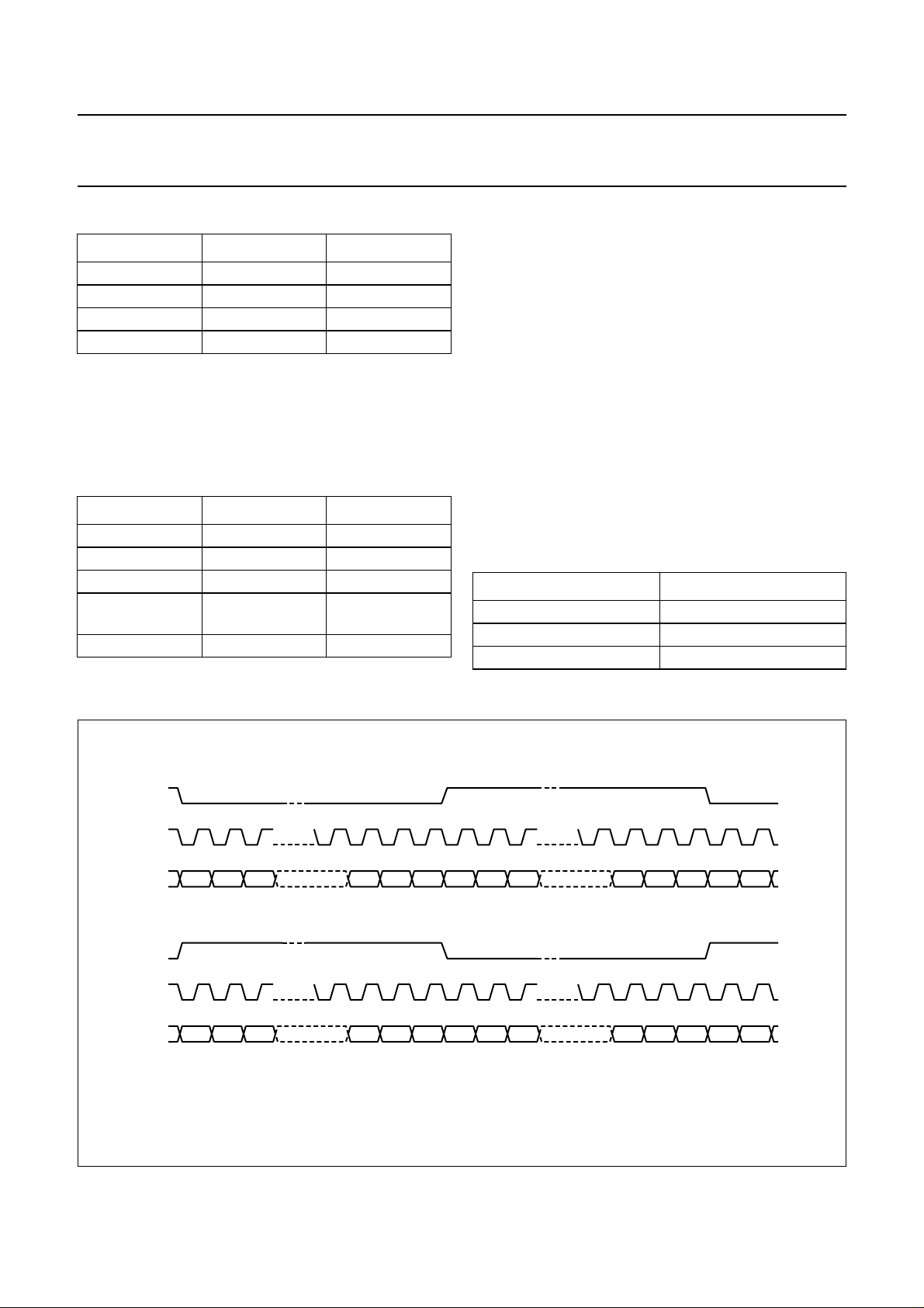
Fig.4 Serial interface master mode timing.
t
t
f
h(WS)
t
su(WS)
h(o)(D)
t
d(o)(D)(BCK)
MGT454
BCK
t
DATAO
T
cy(CLK)(bit)
BCKL
t
d(o)(D)(WS)
Fig.5 Serial interface slave mode timing.
2001 Jan 17 11
t
h(o)(D)
t
d(o)(D)(BCK)
MGT455
Page 12

Philips Semiconductors Product specification
96 kHz sampling 24-bit stereo audio ADC UDA1361TS
APPLICATION INFORMATION
The application information illustrated in Fig.6, is an optimum application environment. Simplification is possible at the
cost of some performance degradation.
handbook, full pagewidth
X5
(63 V)
47 µF
(16 V)
X6
(63 V)
V
DDA
V
DDD
X2-1
X2-2
X2-3
C3
1N
1N
R1
220 Ω
47 µF
(16 V)
47 µF
(16 V)
47 µF
(16 V)
V
X4-1
X4-2
X4-3
R4
47 kΩ
R5
47 kΩ
R10
47 Ω
C11
C12
C4
DDD
C7
100 nF
(63 V)
SYSCLK
116
C6
47 µF
(16 V)
C8
100 nF
(63 V)
R12
47 kΩ
R13
47 kΩ
2
3
4
UDA1361TS
5
6
7
8
R11
47 Ω
15
14
13
12
11
10
C5
47 µF
(16 V)
9
C10
100 nF
(63 V)
47 kΩ
47 kΩ
C9
100 nF
(63 V)
R7
R6
R3
1 Ω
R2
1 Ω
VD
V
DDA
V
X3-1
X3-2
X3-3
X1-1
X1-2
X1-3
X1-4
X1-5
X1-6
X1-7
X1-8
X1-9
X1-10
L1 BLM32A07
L2 BLM32A07
MGU297
DDD
C1
100 µF
(16 V)
V
V
C2
100 µF
(16 V)
DDD
DDA
The capacitors at the input of the ADC can be reduced. It should be noted that the cut-off frequency of the capacitor with the 12 kW input resistance of
the ADC will also change.
Fig.6 Application diagram.
2001 Jan 17 12
Page 13

Philips Semiconductors Product specification
96 kHz sampling 24-bit stereo audio ADC UDA1361TS
PACKAGE OUTLINE
SSOP16: plastic shrink small outline package; 16 leads; body width 4.4 mm
SOT369-1
D
c
y
Z
16
pin 1 index
9
18
w M
b
e
p
E
H
E
A
2
A
1
L
detail X
A
X
v M
A
Q
(A )
L
p
A
3
θ
0 2.5 5 mm
scale
DIMENSIONS (mm are the original dimensions)
UNIT A1A
Note
1. Plastic or metal protrusions of 0.20 mm maximum per side are not included.
A
max.
1.5
0.15
0.00
mm
OUTLINE
VERSION
SOT369-1 MO-152
A3b
2
1.4
0.25
1.2
IEC JEDEC EIAJ
p
0.32
0.20
0.25
0.13
(1)E(1)
cD
5.30
5.10
REFERENCES
4.5
4.3
0.65
2001 Jan 17 13
eHELLpQZywv θ
1.0
0.75
0.45
0.65
0.45
PROJECTION
0.130.2 0.1
EUROPEAN
6.6
6.2
(1)
0.48
0.18
ISSUE DATE
95-02-04
99-12-27
o
10
o
0
Page 14

Philips Semiconductors Product specification
96 kHz sampling 24-bit stereo audio ADC UDA1361TS
SOLDERING
Introduction to soldering surface mount packages
Thistext gives a very brief insight to acomplextechnology.
A more in-depth account of soldering ICs can be found in
our
“Data Handbook IC26; Integrated Circuit Packages”
(document order number 9398 652 90011).
There is no soldering method that is ideal for all surface
mount IC packages. Wave soldering is not always suitable
for surface mount ICs, or for printed-circuit boards with
high population densities. In these situations reflow
soldering is often used.
Reflow soldering
Reflow soldering requires solder paste (a suspension of
fine solder particles, flux and binding agent) to be applied
totheprinted-circuitboardbyscreen printing, stencilling or
pressure-syringe dispensing before package placement.
Several methods exist for reflowing; for example,
infrared/convection heating in a conveyor type oven.
Throughput times (preheating, soldering and cooling) vary
between 100 and 200 seconds depending on heating
method.
Typical reflow peak temperatures range from
215 to 250 °C. The top-surface temperature of the
packages should preferable be kept below 230 °C.
• Use a double-wave soldering method comprising a
turbulent wave with high upward pressure followed by a
smooth laminar wave.
• For packages with leads on two sides and a pitch (e):
– larger than or equal to 1.27 mm, the footprint
longitudinal axis is preferred to be parallel to the
transport direction of the printed-circuit board;
– smaller than 1.27 mm, the footprint longitudinal axis
must be parallel to the transport direction of the
printed-circuit board.
The footprint must incorporate solder thieves at the
downstream end.
• Forpackages with leads on four sides,thefootprint must
be placed at a 45° angle to the transport direction of the
printed-circuit board. The footprint must incorporate
solder thieves downstream and at the side corners.
During placement and before soldering, the package must
be fixed with a droplet of adhesive. The adhesive can be
applied by screen printing, pin transfer or syringe
dispensing. The package can be soldered after the
adhesive is cured.
Typical dwell time is 4 seconds at 250 °C.
A mildly-activated flux will eliminate the need for removal
of corrosive residues in most applications.
Manual soldering
Wave soldering
Conventional single wave soldering is not recommended
forsurface mount devices (SMDs) or printed-circuitboards
with a high component density, as solder bridging and
non-wetting can present major problems.
To overcome these problems the double-wave soldering
method was specifically developed.
If wave soldering is used the following conditions must be
observed for optimal results:
Fix the component by first soldering two
diagonally-opposite end leads. Use a low voltage (24 V or
less) soldering iron applied to the flat part of the lead.
Contact time must be limited to 10 seconds at up to
300 °C.
When using a dedicated tool, all other leads can be
soldered in one operation within 2 to 5 seconds between
270 and 320 °C.
2001 Jan 17 14
Page 15

Philips Semiconductors Product specification
96 kHz sampling 24-bit stereo audio ADC UDA1361TS
Suitability of surface mount IC packages for wave and reflow soldering methods
PACKAGE
WAVE REFLOW
(1)
BGA, LFBGA, SQFP, TFBGA not suitable suitable
SOLDERING METHOD
HBCC, HLQFP, HSQFP, HSOP, HTQFP, HTSSOP, SMS not suitable
(3)
PLCC
, SO, SOJ suitable suitable
LQFP, QFP, TQFP not recommended
SSOP, TSSOP, VSO not recommended
(2)
(3)(4)
(5)
suitable
suitable
suitable
Notes
1. All surface mount (SMD) packages are moisture sensitive. Depending upon the moisture content, the maximum
temperature (with respect to time) and body size of the package, there is a risk that internal or external package
cracks may occur due to vaporization of the moisture in them (the so called popcorn effect). For details, refer to the
Drypack information in the
“Data Handbook IC26; Integrated Circuit Packages; Section: Packing Methods”
.
2. These packages are not suitable for wave soldering as a solder joint between the printed-circuit board and heatsink
(at bottom version) can not be achieved, and as solder may stick to the heatsink (on top version).
3. If wave soldering is considered, then the package must be placed at a 45° angle to the solder wave direction.
The package footprint must incorporate solder thieves downstream and at the side corners.
4. Wave soldering is only suitable for LQFP, TQFP and QFP packages with a pitch (e) equal to or larger than 0.8 mm;
it is definitely not suitable for packages with a pitch (e) equal to or smaller than 0.65 mm.
5. Wave soldering is only suitable for SSOP and TSSOP packages with a pitch (e) equal to or larger than 0.65 mm; it is
definitely not suitable for packages with a pitch (e) equal to or smaller than 0.5 mm.
2001 Jan 17 15
Page 16

Philips Semiconductors Product specification
96 kHz sampling 24-bit stereo audio ADC UDA1361TS
DATA SHEET STATUS
DATA SHEET STATUS
Objective specification Development This data sheet contains the design target or goal specifications for
Preliminary specification Qualification This data sheet contains preliminary data, and supplementary data will be
Product specification Production This data sheet contains final specifications. Philips Semiconductors
Note
1. Please consult the most recently issued data sheet before initiating or completing a design.
DEFINITIONS
Short-form specification The data in a short-form
specification is extracted from a full data sheet with the
same type number and title. For detailed information see
the relevant data sheet or data handbook.
Limiting values definition Limiting values given are in
accordance with the Absolute Maximum Rating System
(IEC 60134). Stress above one or more of the limiting
values may cause permanent damage to the device.
These are stress ratings only and operation of the device
atthese or at any other conditions above those given in the
Characteristics sections of the specification is not implied.
Exposure to limiting values for extended periods may
affect device reliability.
Application information Applications that are
described herein for any of these products are for
illustrative purposes only. Philips Semiconductors make
norepresentation or warranty that suchapplicationswill be
suitable for the specified use without further testing or
modification.
PRODUCT
STATUS
DEFINITIONS
product development. Specification may change in any manner without
notice.
published at a later date. Philips Semiconductors reserves the right to
make changes at any time without notice in order to improve design and
supply the best possible product.
reserves the right to make changes at any time without notice in order to
improve design and supply the best possible product.
DISCLAIMERS
Life support applications These products are not
designed for use in life support appliances, devices, or
systems where malfunction of these products can
reasonably be expected to result in personal injury. Philips
Semiconductorscustomers using or sellingtheseproducts
for use in such applications do so at their own risk and
agree to fully indemnify Philips Semiconductors for any
damages resulting from such application.
Right to make changes Philips Semiconductors
reserves the right to make changes, without notice, in the
products, including circuits, standard cells, and/or
software, described or contained herein in order to
improve design and/or performance. Philips
Semiconductors assumes no responsibility or liability for
theuse of any of these products,conveysno licence or title
under any patent, copyright, or mask work right to these
products,andmakes no representations or warranties that
these products are free from patent, copyright, or mask
work right infringement, unless otherwise specified.
(1)
2001 Jan 17 16
Page 17

Philips Semiconductors Product specification
96 kHz sampling 24-bit stereo audio ADC UDA1361TS
NOTES
2001 Jan 17 17
Page 18

Philips Semiconductors Product specification
96 kHz sampling 24-bit stereo audio ADC UDA1361TS
NOTES
2001 Jan 17 18
Page 19

Philips Semiconductors Product specification
96 kHz sampling 24-bit stereo audio ADC UDA1361TS
NOTES
2001 Jan 17 19
Page 20

Philips Semiconductors – a w orldwide compan y
Argentina: see South America
Australia: 3 Figtree Drive, HOMEBUSH, NSW 2140,
Tel. +61 2 9704 8141, Fax. +61 2 9704 8139
Austria: Computerstr. 6, A-1101 WIEN, P.O. Box 213,
Tel. +43 1 60 101 1248, Fax. +43 1 60 101 1210
Belarus: Hotel Minsk Business Center, Bld. 3, r. 1211, Volodarski Str. 6,
220050 MINSK, Tel. +375 172 20 0733, Fax. +375 172 20 0773
Belgium: see The Netherlands
Brazil: see South America
Bulgaria: Philips Bulgaria Ltd., Energoproject, 15th floor,
51 James Bourchier Blvd., 1407 SOFIA,
Tel. +359 2 68 9211, Fax. +359 2 68 9102
Canada: PHILIPS SEMICONDUCTORS/COMPONENTS,
Tel. +1 800 234 7381, Fax. +1 800 943 0087
China/Hong Kong: 501 Hong Kong Industrial Technology Centre,
72 Tat Chee Avenue, Kowloon Tong, HONG KONG,
Tel. +852 2319 7888, Fax. +852 2319 7700
Colombia: see South America
Czech Republic: see Austria
Denmark: Sydhavnsgade 23, 1780 COPENHAGEN V,
Tel. +45 33 29 3333, Fax. +45 33 29 3905
Finland: Sinikalliontie 3, FIN-02630 ESPOO,
Tel. +358 9 615 800, Fax. +358 9 6158 0920
France: 51 Rue Carnot, BP317, 92156 SURESNES Cedex,
Tel. +33 1 4099 6161, Fax. +33 1 4099 6427
Germany: Hammerbrookstraße 69, D-20097 HAMBURG,
Tel. +49 40 2353 60, Fax. +49 40 2353 6300
Hungary: Philips Hungary Ltd., H-1119 Budapest, Fehervari ut 84/A,
Tel: +36 1 382 1700, Fax: +36 1 382 1800
India: Philips INDIA Ltd, Band Box Building, 2nd floor,
254-D, Dr. Annie Besant Road, Worli, MUMBAI 400 025,
Tel. +91 22 493 8541, Fax. +91 22 493 0966
Indonesia: PT Philips DevelopmentCorporation, Semiconductors Division,
Gedung Philips, Jl. Buncit Raya Kav.99-100, JAKARTA 12510,
Tel. +62 21 794 0040 ext. 2501, Fax. +62 21 794 0080
Ireland: Newstead, Clonskeagh, DUBLIN 14,
Tel. +353 1 7640 000, Fax. +353 1 7640 200
Israel: RAPAC Electronics, 7 Kehilat Saloniki St, PO Box 18053,
TEL AVIV 61180, Tel. +972 3 645 0444, Fax. +972 3 649 1007
Italy: PHILIPS SEMICONDUCTORS, Via Casati, 23 - 20052 MONZA (MI),
Tel. +39 039 203 6838, Fax +39 039 203 6800
Japan: Philips Bldg 13-37, Kohnan 2-chome, Minato-ku,
TOKYO 108-8507, Tel. +81 3 3740 5130, Fax. +81 3 3740 5057
Korea: Philips House, 260-199 Itaewon-dong, Yongsan-ku, SEOUL,
Tel. +82 2 709 1412, Fax. +82 2 709 1415
Malaysia: No. 76 Jalan Universiti, 46200 PETALING JAYA, SELANGOR,
Tel. +60 3 750 5214, Fax. +60 3 757 4880
Mexico: 5900 Gateway East, Suite 200, EL PASO, TEXAS 79905,
Tel. +9-5 800 234 7381, Fax +9-5 800 943 0087
Middle East: see Italy
Netherlands: Postbus 90050, 5600 PB EINDHOVEN, Bldg. VB,
Tel. +31 40 27 82785, Fax. +31 40 27 88399
New Zealand: 2 Wagener Place, C.P.O. Box 1041, AUCKLAND,
Tel. +64 9 849 4160, Fax. +64 9 849 7811
Norway: Box 1, Manglerud 0612, OSLO,
Tel. +47 22 74 8000, Fax. +47 22 74 8341
Pakistan: see Singapore
Philippines: Philips Semiconductors Philippines Inc.,
106 Valero St. Salcedo Village, P.O. Box 2108 MCC, MAKATI,
Metro MANILA, Tel. +63 2 816 6380, Fax. +63 2 817 3474
Poland: Al.Jerozolimskie 195 B, 02-222 WARSAW,
Tel. +48 22 5710 000, Fax. +48 22 5710 001
Portugal: see Spain
Romania: see Italy
Russia: Philips Russia, Ul. Usatcheva 35A, 119048 MOSCOW,
Tel. +7 095 755 6918, Fax. +7 095 755 6919
Singapore: Lorong 1, Toa Payoh, SINGAPORE 319762,
Tel. +65 350 2538, Fax. +65 251 6500
Slovakia: see Austria
Slovenia: see Italy
South Africa: S.A. PHILIPS Pty Ltd., 195-215 Main Road Martindale,
2092 JOHANNESBURG, P.O. Box 58088 Newville 2114,
Tel. +27 11 471 5401, Fax. +27 11 471 5398
South America: Al. Vicente Pinzon, 173, 6th floor,
04547-130 SÃO PAULO, SP, Brazil,
Tel. +55 11 821 2333, Fax. +55 11 821 2382
Spain: Balmes 22, 08007 BARCELONA,
Tel. +34 93 301 6312, Fax. +34 93 301 4107
Sweden: Kottbygatan 7, Akalla, S-16485 STOCKHOLM,
Tel. +46 8 5985 2000, Fax. +46 8 5985 2745
Switzerland: Allmendstrasse 140, CH-8027 ZÜRICH,
Tel. +41 1 488 2741 Fax. +41 1 488 3263
Taiwan: Philips Semiconductors, 5F, No. 96, Chien Kuo N. Rd., Sec. 1,
TAIPEI, Taiwan Tel. +886 2 2134 2451, Fax. +886 2 2134 2874
Thailand: PHILIPS ELECTRONICS (THAILAND) Ltd.,
60/14 MOO 11, Bangna Trad Road KM. 3, Bagna, BANGKOK 10260,
Tel. +66 2 361 7910, Fax. +66 2 398 3447
Turkey: Yukari Dudullu, Org. San. Blg., 2.Cad. Nr. 28 81260 Umraniye,
ISTANBUL, Tel. +90 216 522 1500, Fax. +90 216 522 1813
Ukraine: PHILIPS UKRAINE, 4 Patrice Lumumba str., Building B, Floor 7,
252042 KIEV, Tel. +380 44 264 2776, Fax. +380 44 268 0461
United Kingdom: Philips Semiconductors Ltd., 276 Bath Road, Hayes,
MIDDLESEX UB3 5BX, Tel. +44 208 730 5000, Fax. +44 208 754 8421
United States: 811 East Arques Avenue, SUNNYVALE, CA 94088-3409,
Tel. +1 800 234 7381, Fax. +1 800 943 0087
Uruguay: see South America
Vietnam: see Singapore
Yugoslavia: PHILIPS, Trg N. Pasica 5/v, 11000 BEOGRAD,
Tel. +381 11 3341 299, Fax.+381 11 3342 553
For all other countries apply to: Philips Semiconductors,
Marketing Communications, Building BE-p, P.O. Box 218, 5600 MD EINDHOVEN,
The Netherlands, Fax. +31 40 27 24825
© Philips Electronics N.V. SCA
All rights are reserved. Reproduction in whole or in part is prohibited without the prior written consent of the copyright owner.
The information presented in this document does not form part of any quotation or contract, is believed to be accurate and reliable and may be changed
without notice. No liability will be accepted by the publisher for any consequence of its use. Publication thereof does not convey nor imply any license
under patent- or other industrial or intellectual property rights.
2001
Internet: http://www.semiconductors.philips.com
71
Printed in The Netherlands 753503/01/pp20 Date of release: 2001 Jan 17 Document order number: 9397 750 07157
 Loading...