

Page 1

DATA SH EET
Preliminary specification
Supersedes data of 2000 Jan 27
File under Integrated Circuits, IC01
2000 Feb 04
INTEGRATED CIRCUITS
UDA1344TS
Low-voltage low-power stereo
audio CODEC with DSP features
Page 2
2000 Feb 04 2
Philips Semiconductors Preliminary specification
Low-voltage low-power stereo audio
CODEC with DSP features
UDA1344TS
FEATURES
General
• Low power consumption
• 3.0 V power supply
• System clock of 256fs, 384fsand 512f
s
• Supports sampling frequencies from 8 to 55 kHz
• Non-inverting ADC plus integrated high-pass filter to
cancel DC offset
• ADC supports 2 V (RMS) input signals
• Overload detector for easy record level control
• Separate power control for ADC and DAC
• Integrated digital interpolation filter plus non-inverting
DAC
• Functions controllable either via L3 microcontroller
interface or via static pins
• UDA1344TS is pin and function compatible with
UDA1340M
• Small package size (SSOP28)
• Easy application.
Multiple format input interface
• I2S-bus, MSB-justified or LSB-justified
16, 18 and 20 bits format compatible
• Three combined data formats withMSB-justified output
and LSB-justified 16, 18 and 20 bits input
• 1fsinput and output format data rate.
DAC digital sound processing
The sound processing features of the UDA1344TS can be
used in the L3 mode only:
• Digital tone control, bass boost and treble
• Digital dB-linear volume control (low microcontroller
load) via L3 microcontroller
• Digital de-emphasis for 32, 44.1 and 48 kHz
• Soft mute.
Advanced audio configuration
• Stereo single-ended input configuration
• Stereo line output (under microcontroller volume
control), no post filter required
• High linearity, dynamic range and low distortion.
GENERAL DESCRIPTION
The UDA1344TS is a single-chip stereo Analog-to-Digital
Converter (ADC) and Digital-to-Analog Converter (DAC)
with signal processing features employing bitstream
conversion techniques. The low power consumption and
low voltage requirements make the device eminently
suitable for use in low-voltage low-power portable digital
audio equipment which incorporates recording and
playback functions.
The UDA1344TS supports the I2S-bus data format with
wordlengths of up to 20 bits, the MSB-justified data format
with word lengths of up to 20 bits and the LSB-justified
data format with word lengths of 16, 18 and 20 bits. The
UDA1344TS also supports three combined data formats
with MSB-justified data output and LSB-justified
16, 18 and 20 bits data input.
The UDA1344TS can be controlled either via static pins or
via the L3 interface. In the L3 mode the UDA1344TS has
special Digital Sound Processing (DSP) features in
playback mode such as de-emphasis, volume control,
bass boost, treble and soft mute.
ORDERING INFORMATION
TYPE
NUMBER
PACKAGE
NAME DESCRIPTION VERSION
UDA1344TS SSOP28 plastic shrink small outline package; 28 leads; body width 5.3 mm SOT341-1
Page 3
2000 Feb 04 3
Philips Semiconductors Preliminary specification
Low-voltage low-power stereo audio
CODEC with DSP features
UDA1344TS
QUICK REFERENCE DATA
Notes
1. The input voltage can be up to 2 V (RMS) when the current through the ADC input pin is limited to approximately
1 mA by using a series resistor.
2. The input voltage to the ADC is inversely proportional to the supply voltage.
3. The output voltage of the UDA1344TS differs from the output voltage of the UDA1340M.
4. The output of the DAC scales proportionally with the supply voltage.
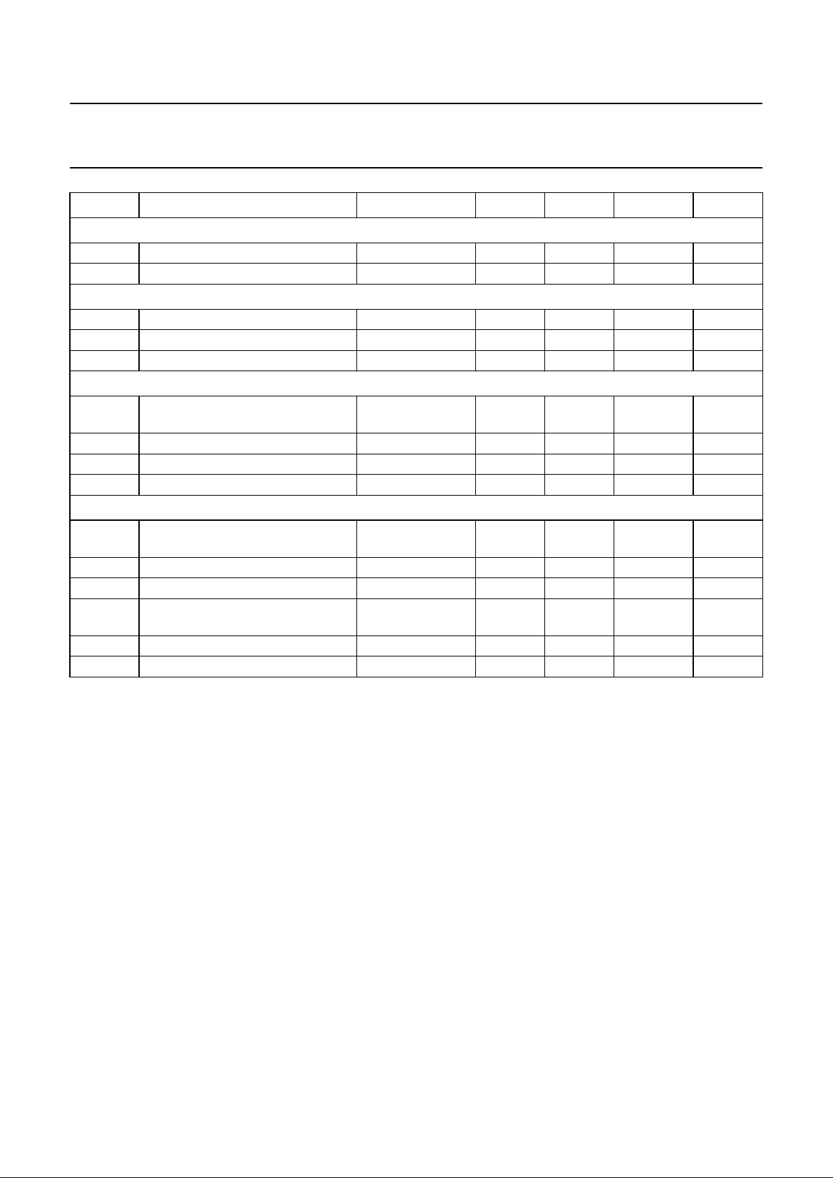
SYMBOL PARAMETER CONDITIONS MIN. TYP. MAX. UNIT
Supplies
V
DDA(ADC)
ADC analog supply voltage 2.7 3.0 3.6 V
V
DDA(DAC)
DAC analog supply voltage 2.7 3.0 3.6 V
V
DDO
operational amplifier supply voltage 2.7 3.0 3.6 V
V
DDD
digital supply voltage 2.7 3.0 3.6 V
I
DDA(ADC)
ADC analog supply current operating − 9.0 11.0 mA
ADC power-down − 3.5 5.0 mA
I
DDA(DAC)
DAC analog supply current operating − 4.0 6.0 mA
DAC power-down − 25 75 µA
I
DDO
operational amplifier supply current operating − 4.0 6.0 mA
DAC power-down − 250 350 µA
I
DDD
digital supply current operating − 6.0 9.0 mA
DAC power-down − 2.5 4.0 mA
ADC power-down − 3.5 5.0 mA
T
amb
ambient temperature −40 − +85 °C
Analog-to-digital converter
V
i(rms)
input voltage (RMS value) notes 1 and 2 − 1.0 − V
(THD + N)/S total harmonic distortion-plus-noise to
signal ratio
at 0 dB −−85 −80 dB
at −60 dB; A-weighted −−35 −30 dB
S/N signal-to-noise ratio V
i
= 0 V; A-weighted − 95 − dB
α
cs
channel separation − 100 − dB
Digital-to-analog converter
V
o(rms)
output voltage (RMS value) notes 3 and 4 − 900 − mV
(THD + N)/S total harmonic distortion-plus-noise to
signal ratio
at 0 dB −−90 −85 dB
at −60 dB; A-weighted −−37 − dB
S/N signal-to-noise ratio code = 0; A-weighted − 100 − dB
α
cs
channel separation − 100 − dB
Power performance
P
ADDA
power consumption in record and
playback mode
− 69 − mW
P
DA
power consumption in playback mode − 42 − mW
P
AD
power consumption in record mode − 37.5 − mW
P
PD
power consumption in power-down mode − 17 − mW
Page 4
2000 Feb 04 4
Philips Semiconductors Preliminary specification
Low-voltage low-power stereo audio
CODEC with DSP features
UDA1344TS
BLOCK DIAGRAM
Fig.1 Block diagram.
handbook, full pagewidth
MGL441
ADC
0 dB/6 dB
SWITCH
0 dB/6 dB
SWITCH
3
5
10
11
18
16
17
19
25 27 23 22
12
15
14
13
20
21
8
VINL
V
DDD
V
SSD
DATAO
BCK
WS
DATAI
MP1
VOUTL
28
24
9
26
VOUTR
SYSCLK
MP4
MP3
MP2
MP5
MC2
MC1
VINR
21
76 4
DECIMATION FILTER
DC-CANCELLATION FILTER
DIGITAL INTERFACE
L3-BUS
INTERFACE
ADC
DAC
V
ref(D)
V
DDO
V
SSO
DAC
INTERPOLATION FILTER
NOISE SHAPER
DSP FEATURES
V
DDA(ADC)VSSA(ADC)
V
ADCP
V
ADCN
V
ref(A)
UDA1344TS
V
DDA(DAC)VSSA(DAC)
Page 5
2000 Feb 04 5
Philips Semiconductors Preliminary specification
Low-voltage low-power stereo audio
CODEC with DSP features
UDA1344TS
PINNING
SYMBOL PIN DESCRIPTION
V
SSA(ADC)
1 ADC analog ground
V
DDA(ADC)
2 ADC analog supply voltage
VINL 3 ADC input left
V
ref(A)
4 ADC reference voltage
VINR 5 ADC input right
V
ADCN
6 ADC negative reference voltage
V
ADCP
7 ADC positive reference voltage
MC1 8 mode control 1 input (pull-down)
MP1 9 multi purpose pin 1 output
V
DDD
10 digital supply voltage
V
SSD
11 digital ground
SYSCLK 12 system clock input:
256f
s
, 384fsor 512f
s
MP2 13 multi purpose pin 2 input
MP3 14 multi purpose pin 3 input
MP4 15 multi purpose pin 4 input
BCK 16 bit clock input
WS 17 word select input
DATAO 18 data output
DATAI 19 data input
MP5 20 multi purpose pin 5 output
(pull-down)
MC2 21 mode control 2 input (pull-down)
V
SSA(DAC)
22 DAC analog ground
V
DDA(DAC)
23 DAC analog supply voltage
VOUTR 24 DAC output right
V
DDO
25 operational amplifier supply voltage
VOUTL 26 DAC output left
V
SSO
27 operational amplifier ground
V
ref(D)
28 DAC reference voltage
Fig.2 Pin configuration.
handbook, halfpage
V
SSA(ADC)
V
DDA(ADC)
VINL
V
ref(A)
VINR
V
ADCN
V
ADCP
MC1
MP1
V
DDD
V
SSD
SYSCLK
MP2
MP3
V
ref(D)
V
SSO
VOUTL
V
DDO
V
DDA(DAC)
V
SSA(DAC)
VOUTR
MC2
MP5
DATAI
DATAO
WS
BCK
MP4
1
2
3
4
5
6
7
8
9
10
11
12
13
28
27
26
25
24
23
22
21
20
19
18
17
16
1514
UDA1344TS
MGL442
Page 6
2000 Feb 04 6
Philips Semiconductors Preliminary specification
Low-voltage low-power stereo audio
CODEC with DSP features
UDA1344TS
FUNCTIONAL DESCRIPTION
The UDA1344TS accommodates slave mode only, this
means that in all applications the system devices must
provide the system clock. The system clock must be
locked in frequency to the digital interface input signals.
The BCK clock can be up to 128fs, or in other words the
BCK frequency is 128 times the Word Select (WS)
frequency or less: f
BCK
= < 128 × fWS.
Remarks:
1. The WS edge MUST fall on the negative edge of the
BCKclockatalltimesforproperoperationofthedigital
I/O data interface
2. The sampling frequency range is from 5 to 55 kHz
3. For MSB- and LSB-justified formats it is important to
have a WS signal with a duty factor of 50%.
Analog-to-Digital Converter (ADC)
The stereo ADC of the UDA1344TS consists of two
3rd-order Sigma-Delta modulators. They have a modified
Ritchie-coder architecture in a differential switched
capacitor implementation. The oversampling ratio is 128.
In contrast to the UDA1340M, the UDA1344TS supports
1 V (RMS) input signals and can be set, via an external
resistor, to support 2 V (RMS) input signals.
Analog front-end
The analog front-end is equippedwith a selectable 0 dBor
6 dB gain block. The pin to select the gain switch is given
in Section “L3 mode”. This block can be used in
applications in which both 1 V (RMS) and 2 V (RMS) input
signals are available.
In applications in which a 2 V (RMS) input signal is used,
a12kΩresistormust be connected in serieswith the input
of the ADC. This makes a voltage divider with the internal
ADC resistor and makes sure only 1 V (RMS) maximum is
inputto the IC. Using this application for a 2 V (RMS) input
signal, the gain switch must be set to 0 dB. When a
1 V (RMS) input signal is input to the ADC in the same
application, the gain switch must be set to 6 dB.
An overview of the maximum input voltages allowed
againstthepresenceofanexternalresistor and the setting
of the gain switch is given in Table 1.
Table 1 Application modes using input gain stage
Decimation filter (ADC)
The decimation from 128fsto 1fsis performed in 2 stages.
Thefirst stage realizes 3rd-order characteristic.This
filter decreases the sample rate by 16.
The second stage, a Finite Impulse Response (FIR) filter,
consists of 3 half-band filters, each decimating by a factor
of 2.
Table 2 Decimation filter characteristics
DC-cancellation filter (ADC)
AnoptionalInfiniteImpulse-Response(IIR)high-passfilter
is provided to remove unwanted DC components.
The operation is selected by the microcontroller via the
L3 interface. The filter characteristics are given in Table 3.
Table 3 DC-cancellation filter characteristics
RESISTOR
(12 kΩ)
INPUT GAIN
SWITCH
MAXIMUM
INPUT
VOLTAGE
Present 0 dB 2 V (RMS)
Present 6 dB 1 V (RMS)
Absent 0 dB 1 V (RMS)
Absent 6 dB 0.5 V (RMS)
ITEM CONDITIONS VALUE (dB)
Pass-band ripple 0 − 0.45f
s
±0.05
Stop band >0.55f
s
−60
Dynamic range 0 − 0.45f
s
108
Overall gain with
0 dB input to the
ADC
DC −1.16
ITEM CONDITIONS VALUE (dB)
Pass-band ripple − none
Pass-band gain − 0
Droop at 0.00045f
s
0.031
Attenuation at DC at 0.00000036f
s
>40
Dynamic range 0 − 0.45f
s
>110
sin x
x
----------- -
Page 7
2000 Feb 04 7
Philips Semiconductors Preliminary specification
Low-voltage low-power stereo audio
CODEC with DSP features
UDA1344TS
Mute (ADC)
On recovery from power-down or switching on of the
system clock, the serial data output on pin DATAO is held
at LOW level until valid data is available from the
decimation filter. This time depends on whether the
DC-cancellation filter is selected:
• DC cancel off:
; t = 23.2 ms at f
s
= 44.1 kHz
• DC cancel on:
; t = 279 ms at f
s
= 44.1 kHz.
Interpolation filter (DAC)
The digital filter interpolates from 1f
s
to 128fsby means of
a cascade of a recursive filter and an FIR filter.
Table 4 Interpolation filter characteristics
Noise shaper (DAC)
The 3rd-order noise shaper operates at 128fs. It shifts
in-band quantization noise to frequencies well above the
audio band. This noise shaping technique enables high
signal-to-noise ratios to be achieved. The noise shaper
output is converted into an analog signal using a Filter
Stream Digital-to-Analog Converter (FSDAC).
Filter stream DAC
The FSDAC is a semi-digital reconstruction filter that
converts the 1-bit data stream of the noise shaper to an
analog output voltage. The filter coefficients are
implemented as current sources and are summed at
virtual ground of the output operational amplifier. In this
way very high signal-to-noise performance and low clock
jitter sensitivity is achieved. A post-filter is not needed due
to the inherent filter function of the DAC. On-board
amplifiers convert the FSDAC output current to an output
voltage signal capable of driving a line output.
The output voltage of the FSDAC scales proportionally
with the power supply voltage.
ITEM CONDITIONS VALUE (dB)
Pass-band ripple 0 − 0.45f
s
±0.03
Stop band >0.55f
s
−50
Dynamic range 0 − 0.45f
s
108
Gain DC −3.5
t
1024
f
s
------------ -
=
t
12288
f
s
----------------
=
Multiple format input/output interface
The UDA1344TS supports the following data input/output
formats:
• I2S-bus format with data word length of up to 20 bits
• MSB-justifiedserialformatwithdatawordlength of up to
20 bits
• LSB-justified serial format with data word lengths of
16, 18 or 20 bits (in L3 mode only)
• Combined data formats:
– L3 mode: MSB-justified data output and
LSB-justified 16, 18 and 20 bits data input
– Static pin mode: MSB-justified data output and
LSB-justified 16 and 20 bits data input.
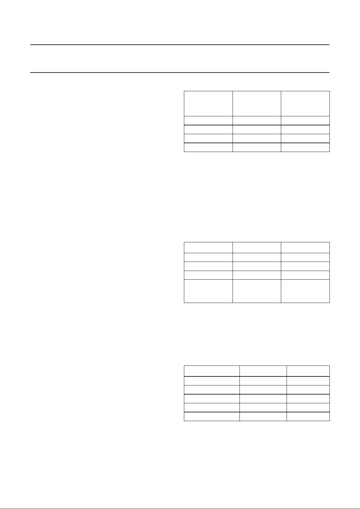
The formats are illustrated in Fig.3. Left and right
data-channel words are time multiplexed.
Control mode selection
The UDA1344TS can be used under L3 microcontroller
interface control or static pin control. The mode can be set
via the mode control pins MC1 and MC2 (see Table 5).
Table 5 Mode control pins
Important: in the L3 mode the UDA1344TS is completely
pin and function compatible with the UDA1340M.
PIN MC2 PIN MC1 MODE
LOW LOW L3 mode
LOW HIGH Test mode
HIGH LOW
HIGH HIGH Static pin mode
Page 8
2000 Feb 04 8
Philips Semiconductors Preliminary specification
Low-voltage low-power stereo audio
CODEC with DSP features
UDA1344TS
This text is here in white to force landscape pages to be rotated correctly when browsing through the pdf in the Acrobat reader.This text is here in
_white to force landscape pages to be rotated correctly when browsing through the pdf in the Acrobat reader.This text is here inThis text is here in
white to force landscape pages to be rotated correctly when browsing through the pdf in the Acrobatreader. white to force landscapepages to be ...
d
book, full pagewidth
16
MSB B2 B3 B4 B5 B6
LEFT
LSB-JUSTIFIED FORMAT 20 BITS
WS
BCK
DATA
RIGHT
1518 1720 19 2 1
B19
LSB
16
MSB B2 B3 B4 B5 B6
1518 1720 19 2 1
B19 LSB
MSB MSBB2
21> = 812 3
LEFT
I
2
S-BUS FORMAT
WS
BCK
DATA
RIGHT
3
> = 8
MSB B2
MBL140
16
MSB
B2
LEFT
LSB-JUSTIFIED FORMAT 16 BITS
WS
BCK
DATA
RIGHT
15 2 1
B15
LSB
16
MSB B2
15 2 1
B15 LSB
16
MSB B2 B3 B4
LEFT
LSB-JUSTIFIED FORMAT 18 BITS
WS
BCK
DATA
RIGHT
1518 17 2 1
MSB B2 B3 B4
B17
LSB
16 1518 17 2 1
B17 LSB
MSB-JUSTIFIED FORMAT
WS
LEFT
RIGHT
321321
MSB B2 MSBLSB LSB MSB B2B2
> = 8 > = 8
BCK
DATA
Fig.3 Serial interface formats.
Page 9
2000 Feb 04 9
Philips Semiconductors Preliminary specification
Low-voltage low-power stereo audio
CODEC with DSP features
UDA1344TS
Static pin mode
The UDA1344TS is set to static pin mode by setting both
pins MC1 and MC2 to HIGH level.
The controllable features in this mode are:
• System clock frequency selection
• Data input/output format selection
• De-emphasis and mute control
• Power-down and ADC input level selection.
PINNING DEFINITION
The pinning definition in the static pin mode is given in
Table 6.
Table 6 Pinning definition in static pin model
S
YSTEM CLOCK
In the static pin mode the options are 256fs and 384fs as
given in Table 7.
Table 7 System clock selection
M
UTE AND DE-EMPHASIS
The level definition of pin MP2 pin is given in Table 8.
Table 8 Levels for pin MP2
I
NPUT/OUTPUT DATA FORMAT SELECTION
The input/output data format can be selected using
pins MP1 and MP5 as given in Table 9.
Table 9 Data format selection
ADC INPUT VOLTAGE SELECTION AND POWER-DOWN
In the static pin mode the three-level pin MP4 is used to
select 0 or 6 dB gain and power-down.
Table 10 Levels for pin MP4
PIN DESCRIPTION
MP1 data input/output setting
MP2 three-level pin to select no
de-emphasis, de-emphasis or mute
MP3 256f
s
or 384fssystem clock selection
MP4 three-level pin to select
ADC power-down, ADC input
1 V (RMS) or ADC input 2 V (RMS)
MP5 data input/output setting
PIN MP3 SELECTION
LOW 256f
s
clock frequency
HIGH 384f
s
clock frequency
PIN MP2 SELECTION
LOW no de-emphasis and mute
0.5V
DDD
de-emphasis 44.1 kHz
HIGH mute
PIN MP1 PIN MP5 SELECTION
LOW LOW input: MSB-justified
LOW HIGH input: I
2
S-bus
HIGH LOW input: LSB-justified 20 bits;
output: MSB-justified
HIGH HIGH input: LSB-justified 16 bits;
output: MSB-justified
PIN MP4 SELECTION
LOW ADC power-down
0.5V
DDD
6 dB gain
HIGH 0 dB gain
Page 10

2000 Feb 04 10
Philips Semiconductors Preliminary specification
Low-voltage low-power stereo audio
CODEC with DSP features
UDA1344TS
L3 mode
The UDA1344TS is set to the L3 mode by setting both
pins MC1 and MC2 to LOW level.
The static pins in this mode are used for:
• ADC output overload detection
• L3 interface signal input
• ADC input voltage selection.
The controllable features via the L3 interface and the
definition of the control registers are given in
Section “L3 interface”.
PINNING DEFINITION
The pinning definition in the L3 mode is given in Table 11.
Table 11 Pinning definition in L3 mode
ADC OUTPUT OVERLOAD DETECTION
In practice the output is used to indicate whenever the
output data, in either the left or right channel, is greater
than −1 dB (actual figure is −1.16 dB) of the maximum
possible digital swing. When this condition is detected
pin MP1 is forced to HIGH level for at least 512fscycles
(11.6 ms at fs= 44.1 kHz). This time-out is reset for each
infringement.
ADC INPUT VOLTAGE SELECTION
In the L3 mode pin MP5 is used to select 0 or 6 dB gain.
Table 12 Levels for pin MP5
PIN FUNCTION
MP1 ADC output overload detection
MP2 L3MODE input
MP3 L3CLOCK input
MP4 L3DATA input
MP5 ADC input voltage selection:
1 V (RMS) or 2 V (RMS)
PIN MP4 SELECTION
LOW 0 dB gain
HIGH 6 dB gain
Page 11

2000 Feb 04 11
Philips Semiconductors Preliminary specification
Low-voltage low-power stereo audio
CODEC with DSP features
UDA1344TS
L3 INTERFACE
The UDA1344TS has a microcontroller input mode. In the
microcontroller control mode, all the digital sound
processing features and the system controlling features
can be controlled by the microcontroller. The controllable
features are:
• System clock frequency
• Data input format
• Power control
• DC filtering
• De-emphasis
• Volume
• Flat/min./max. switch
• Bass boost
• Treble
• Mute.
Theexchange of data and control information betweenthe
microcontroller and the UDA1344TS is accomplished
through a serial hardware interface comprising the
following lines:
L3DATA: microcontroller interface data line
L3MODE: microcontroller interface mode line
L3CLOCK: microcontroller interface clock line.
Information transfer via the microcontroller bus is LSB first
and is organized in accordance with the so called
‘L3’ format, in which two different modes of operation can
be distinguished: address mode and data transfer mode.
The address mode is required to select a device
communicating via the L3 interface and to define the
destination registers for the data transfer mode. Data
transfer for the UDA1344TS can only be in one direction:
input to the UDA1344TS to program its sound processing
and other functional features.
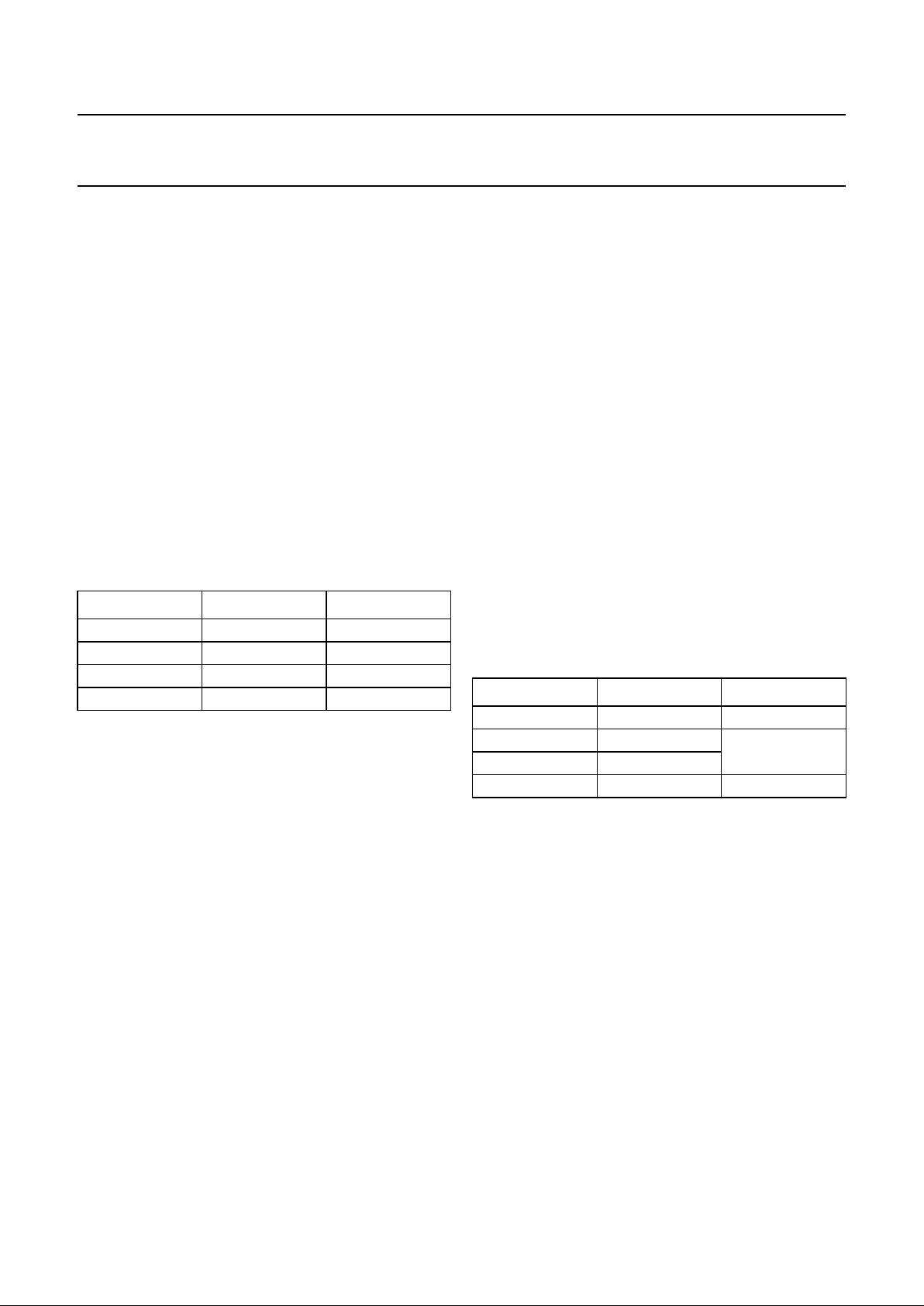
Address mode
The address mode is used to select a device for
subsequent data transfer and to define the destination
registers. The address mode ischaracterized by L3MODE
being LOW and a burst of 8 pulses on L3CLOCK,
accompanied by 8 data bits.
The fundamental timing is shown in Fig.4.
Data bits 7 to 2 represent a 6-bitdevice address, with bit 7
being the MSB and bit 2 the LSB. The address of the
UDA1344TS is 000101 (bits 7 to 2).
Data bits 1 and 0 indicate the type of subsequent data
transfer as given in Table 13.
Table 13 Selection of data transfer
In the event that the UDA1344TS receives a different
address, it will deselect its microcontroller interface logic.
Data transfer mode
The selection preformed in the address mode remains
active during subsequent data transfers, until the
UDA1344TS receives a new address command.
The fundamental timing of data transfers is essentially the
same as in the address mode and is shown in Fig.5.
The maximum input clock and data rate is 64fs.
All transfers are byte wise, i.e. they are based on groups
of 8 bits. Data will be stored in the UDA1344TS after the
eighth bit of a byte has been received.
A multibyte data transfer is illustrated in Fig.6.
Programming the sound processing and other
features
The sound processing and other feature values are stored
in independent registers.
Thefirstselectionoftheregistersisachieved by the choice
of data type that is transferred. This is performed in the
address mode by bit 1 and bit 0 (see Table 13).
The second selection is performed by the 2 MSBs of the
data byte (bit 7 and bit 6).
The other bits in the data byte (bits 5 to 0) is the value that
is placed in the selected registers.
BIT 1 BIT 0 TRANSFER
0 0 data (volume, bass boost, treble,
de-emphasis, mute, mode and
power control)
0 1 not used
1 0 status (system clock frequency,
data input/output format and
DC filter)
1 1 not used
Page 12

2000 Feb 04 12
Philips Semiconductors Preliminary specification
Low-voltage low-power stereo audio
CODEC with DSP features
UDA1344TS
handbook, full pagewidth
t
h(L3)A
t
h(L3)DA
t
su(L3)DA
T
cy(CLK)(L3)
BIT 0
L3MODE
L3CLOCK
L3DATA
BIT 7
MGL723
t
CLK(L3)H
t
CLK(L3)L
t
su(L3)A
t
su(L3)A
t
h(L3)A
Fig.4 Timing in address mode.
handbook, full pagewidth
t
stp(L3)
t
stp(L3)
t
su(L3)D
t
su(L3)DA
t
h(L3)DA
t
h(L3)D
MGL882
T
cy(CLK)L3
L3MODE
L3CLOCK
t
CLK(L3)H
t
CLK(L3)L
BIT 0
L3DATA
WRITE
BIT 7
Fig.5 Timing in data transfer mode.
Page 13

2000 Feb 04 13
Philips Semiconductors Preliminary specification
Low-voltage low-power stereo audio
CODEC with DSP features
UDA1344TS
handbook, full pagewidth
t
stp(L3)
address
L3DATA
L3CLOCK
L3MODE
addressdata byte #1 data byte #2
MGL725
Fig.6 Multibyte data transfer.
L3 interface registers
When the data transfer of type ‘status’ is selected, the features system clock frequency, data input format and DC filter
can be controlled.
Table 14 Data transfer of type ‘status’
When the data transfer of type ‘data’ is selected, the features volume, bass boost, treble, de-emphasis, mute, mode and
power control can be controlled.
Table 15 Data transfer of type ‘data’
BIT 7 BIT 6 BIT 5 BIT 4 BIT 3 BIT 2 BIT 1 BIT 0 REGISTER SELECTED
0 0 SC1 SC0 IF2 IF1 IF0 DC SC = system clock frequency (2 bits); see Table 16
IF = data input format (3 bits); see Table 17
DC = DC filter (1 bit); see Table 18
BIT 7 BIT 6 BIT 5 BIT 4 BIT 3 BIT 2 BIT 1 BIT 0 REGISTER SELECTED
0 0 VC5 VC4 VC3 VC2 VC1 VC0 VC = volume control (6 bits); see Table 19
0 1 BB3 BB2 BB1 BB0 TR1 TR0 BB = bass boost (4 bits); see Table 20
TR = treble (2 bits); see Table 21
1 0 0 DE1 DE0 MT M1 M0 DE = de-emphasis (2 bits); see Table 22
MT = mute (1 bit); see Table 23
M = filter mode (2 bits); see Table 24
110000PC1PC0PC=power control (2 bits); see Table 25
Page 14

2000 Feb 04 14
Philips Semiconductors Preliminary specification
Low-voltage low-power stereo audio
CODEC with DSP features
UDA1344TS
SYSTEM CLOCK FREQUENCY
A 2-bit value to select the used external clock frequency.
Table 16 System clock frequency settings
DATA INPUT FORMAT
A 3-bit value to select the used data format.
Table 17 Data format settings
DC FILTER
A 1-bit value to enable the digital DC filter.
Table 18 DC filtering
VOLUME CONTROL
A 6-bit value to program the left and right channel volume
attenuation. The range is from 0 to −∞ dB in steps of 1 dB.
Table 19 Volume settings
BASS BOOST
A 4-bit value to program the bass boost setting. The used
set depends on the mode bits M1 and M0.
Table 20 Bass boost settings
SC1 SC0 SELECTION
0 0 512f
s
0 1 384f
s
1 0 256f
s
1 1 not used
IF2 IF1 IF0 FORMAT
000I
2
S-bus
0 0 1 LSB-justified 16 bits
0 1 0 LSB-justified 18 bits
0 1 1 LSB-justified 20 bits
1 0 0 MSB-justified
1 0 1 input: LSB-justified 16 bits;
output: MSB-justified
1 1 0 input: LSB-justified 18 bits;
output: MSB-justified
1 1 1 input: LSB-justified 20 bits;
output: MSB-justified
DC SELECTION
0 no DC filtering
1 DC filtering
VC5 VC4 VC3 VC2 VC1 VC0 VOLUME (dB)
000000 0
000001 0
000010 −1
000011 −2
:::::: :
111011 −58
111100 −59
111101 −60
111110 −∞
111111 −∞
BB3 BB2 BB1 BB0
BASS BOOST SETTING
FLAT
(dB)
MIN.
(dB)
MAX.
(dB)
0000 0 0 0
0001 0 2 2
0010 0 4 4
0011 0 6 6
0100 0 8 8
0101 0 10 10
0110 0 12 12
0111 0 14 14
1000 0 16 16
1001 0 18 18
1010 0 18 20
1011 0 18 22
1100 0 18 24
1101 0 18 24
1110 0 18 24
1111 0 18 24
Page 15

2000 Feb 04 15
Philips Semiconductors Preliminary specification
Low-voltage low-power stereo audio
CODEC with DSP features
UDA1344TS
TREBLE
A 2-bit value to program the treble setting. The used set
depends on the mode bits M1 and M0.
Table 21 Treble settings
DE-EMPHASIS
A 2-bit value to enable the digital de-emphasis filter.
Table 22 De-emphasis settings
MUTE
A 1-bit value to enable the digital mute.
Table 23 Mute
MODE
A2-bit value to program the mode of thesoundprocessing
filters of bass boost and treble.
Table 24 Flat/min./max. switch
POWER CONTROL
A 2-bit value to disable the ADC and/or DAC to reduce
power consumption.
Table 25 Power control settings
TR1 TR0
TREBLE SETTING
FLAT (dB) MIN. (dB) MAX. (dB)
00000
01022
10044
11066
DE1 DE0 SELECTION
0 0 no de-emphasis
0 1 de-emphasis 32 kHz
1 0 de-emphasis 44.1 kHz
1 1 de-emphasis 48 kHz
MT SELECTION
0 no muting
1 muting
M1 M0 SELECTION
0 0 flat
0 1 min.
1 0 min.
1 1 max.
PC1 PC0
SELECTION
ADC DAC
0 0 off off
0 1 off on
1 0 on off
1 1 on on
Page 16

2000 Feb 04 16
Philips Semiconductors Preliminary specification
Low-voltage low-power stereo audio
CODEC with DSP features
UDA1344TS
LIMITING VALUES
In accordance with the Absolute Maximum Rating System (IEC 60134).
Notes
1. Equivalent to discharging a 100 pF capacitor via a 1.5 kΩ series resistor.
2. Equivalent to discharging a 200 pF capacitor via a 2.5 µH series inductor.
THERMAL CHARACTERISTICS
DC CHARACTERISTICS
V
DDD=VDDA=VDDO
= 3.0 V; T
amb
=25°C; RL=5kΩ; all voltages referenced to ground; unless otherwise specified.
SYMBOL PARAMETER CONDITIONS MIN. MAX. UNIT
V
DDD
digital supply voltage − 5.0 V
T
xtal(max)
maximum crystal temperature − 150 °C
T
stg
storage temperature −65 +125 °C
T
amb
ambient temperature −40 +85 °C
V
es
electrostatic handling voltage note 1 −3000 +3000 V
note 2 −300 +300 V
SYMBOL PARAMETER CONDITIONS VALUE UNIT
R
th(j-a)
thermal resistance from junction to ambient in free air 90 K/W
SYMBOL PARAMETER CONDITIONS MIN. TYP. MAX. UNIT
Supplies; note 1
V
DDA(ADC)
ADC analog supply voltage 2.7 3.0 3.6 V
V
DDA(DAC)
DAC analog supply voltage 2.7 3.0 3.6 V
V
DDO
operational amplifier supply voltage 2.7 3.0 3.6 V
V
DDD
digital supply voltage 2.7 3.0 3.6 V
I
DDA(ADC)
ADC analog supply current operating − 9.0 11.0 mA
ADC power-down − 3.5 5.0 mA
I
DDA(DAC)
DAC analog supply current operating − 4.0 6.0 mA
DAC power-down − 25 75 µA
I
DDO
operational amplifier supply current operating − 4.0 6.0 mA
DAC power-down − 250 300 µA
I
DDD
digital supply current operating − 6.0 9.0 mA
DAC power-down − 2.5 4.0 mA
ADC power-down − 3.5 5.0 mA
Digital inputs
V
IH
HIGH-level input voltage 0.8V
DDD
− V
DDD
+ 0.5 V
V
IL
LOW-level input voltage −0.5 − 0.2V
DDD
V
I
LI
input leakage current −−10 µA
C
i
input capacitance −−10 pF
Page 17
2000 Feb 04 17
Philips Semiconductors Preliminary specification
Low-voltage low-power stereo audio
CODEC with DSP features
UDA1344TS
Notes
1. All power supply pins (VDDand VSS) must be connected to the same external power supply unit.
2. When higher capacitive loads must be driven, a 100 Ω resistor must be connected in series with the DAC output in
order to prevent oscillations in the output operational amplifier.
Digital outputs
V
OH
HIGH-level output voltage IOH= −2 mA 0.85V
DDD
−− V
V
OL
LOW-level output voltage IOL=2mA −−0.4 V
Three-level inputs: pins MP2 and MP4
V
IH
HIGH-level input voltage 0.9V
DDD
− V
DDD
+ 0.5 V
V
IM
MIDDLE-level input voltage 0.4V
DDD
− 0.6V
DDD
V
V
IL
LOW-level input voltage −0.5 − 0.1V
DDD
V
Analog-to-digital converter
V
ref(A)
reference voltage referenced to
V
SSA(ADC)
0.45V
DDA
0.5V
DDA
0.55V
DDA
V
R
o(refA)
output resistance on pin V
ref(A)
− 24 − kΩ
R
i
input resistance fi= 1 kHz − 9.8 − kΩ
C
i
input capacitance − 20 − pF
Digital-to-analog converter
V
ref(D)
reference voltage referenced to
V
SSA(DAC)
0.45V
DDA
0.5V
DDA
0.55V
DDA
V
R
o(refD)
output resistance on pin V
ref(D)
− 28 − kΩ
R
o
output resistance of DAC − 0.13 3.0 Ω
I
o(max)
maximum output current (THD + N)/S < 0.1
%; RL=5kΩ
− 0.22 − mA
R
L
load resistance 3 −− kΩ
C
L
load capacitance note 2 −−200 pF
SYMBOL PARAMETER CONDITIONS MIN. TYP. MAX. UNIT
Page 18

2000 Feb 04 18
Philips Semiconductors Preliminary specification
Low-voltage low-power stereo audio
CODEC with DSP features
UDA1344TS
AC CHARACTERISTICS
V
DDD=VDDA=VDDO
= 3.0 V; fi= 1 kHz; T
amb
=25°C; RL=5kΩ; all voltages referenced to ground; unless otherwise
specified.
Notes
1. The input voltage can be up to 2 V (RMS) when the current through the ADC input pin is limited to approximately
1 mA by using a series resistor.
2. The input voltage to the ADC is inversely proportional with the supply voltage.
3. The output voltage of the UDA1344TS differs from the output voltage of the UDA1340M.
4. The output of the DAC scales proportionally with the supply voltage.
SYMBOL PARAMETER CONDITIONS TYP. MAX. UNIT
Analog-to-digital converter
V
i(rms)
input voltage (RMS value) notes 1 and 2 1.0 − V
∆V
i
unbalance between channels 0.1 − dB
(THD + N)/S total harmonic distortion-plus-noise to signal ratio at 0 dB −85 −80 dB
at −60 dB; A-weighted −35 −30 dB
S/N signal-to-noise ratio V
i
= 0 V; A-weighted 95 − dB
α
cs
channel separation 100 − dB
PSRR power supply rejection ratio f
ripple
= 1 kHz;
V
ripple
= 300 mV (p-p)
30 − dB
Digital-to-analog converter
V
o(rms)
output voltage (RMS value) notes 3 and 4 900 − mV
∆V
o
unbalance between channels 0.1 − dB
(THD + N)/S total harmonic distortion-plus-noise to signal ratio at 0 dB −90 −85 dB
at −60 dB; A-weighted −37 − dB
S/N signal-to-noise ratio code = 0; A-weighted 100 − dB
α
cs
channel separation 100 − dB
PSRR power supply rejection ratio f
ripple
= 1 kHz;
V
ripple
= 300 mV (p-p)
50 − dB
Page 19

2000 Feb 04 19
Philips Semiconductors Preliminary specification
Low-voltage low-power stereo audio
CODEC with DSP features
UDA1344TS
TIMING
V
DDD=VDDA=VDDO
= 2.7 to 3.6 V; T
amb
= −40 to +85 °C; RL=5kΩ; all voltages referenced to ground; unless
otherwise specified.
SYMBOL PARAMETER CONDITIONS MIN. TYP. MAX. UNIT
System clock input (see Fig.7)
T
sys
system clock cycle time f
sys
= 256f
s
78 88 262 ns
f
sys
= 384f
s
52 59 174 ns
f
sys
= 512f
s
39 44 132 ns
t
CWH
system clock HIGH time f
sys
< 19.2 MHz 0.30T
sys
− 0.70T
sys
ns
f
sys
≥ 19.2 MHz 0.40T
sys
− 0.60T
sys
ns
t
CWL
system clock LOW time f
sys
< 19.2 MHz 0.30T
sys
− 0.70T
sys
ns
f
sys
≥ 19.2 MHz 0.40T
sys
− 0.60T
sys
ns
Serial interface input/output data (see Fig.8)
f
BCK
bit clock frequency −−64f
s
Hz
T
cy(BCK)
bit clock cycle time T
cy(s)
= cycle time of
sample frequency
−− ns
t
BCKH
bit clock HIGH time 100 −− ns
t
BCKL
bit clock LOW time 100 −− ns
t
r
rise time −−20 ns
t
f
fall time −−20 ns
t
su(WS)
word select set-up time 20 −− ns
t
h(WS)
word select hold time 10 −− ns
t
su(DATAI)
data input set-up time 20 −− ns
t
h(DATAI)
data input hold time 0 −− ns
t
h(DATAO)
data output hold time 0 −− ns
t
d(DATAO−BCK)
data output to bit clock delay from BCK falling edge −−80 ns
t
d(DATAO−WS)
data output to word select delay from WS edge for
MSB-justified format
−−80 ns
L3 interface input (see Figs 4 and 5)
T
cy(CLK)L3
L3CLOCK cycle time 500 −− ns
t
CLK(L3)H
L3CLOCK HIGH time 250 −− ns
t
CLK(L3)L
L3CLOCK LOW time 250 −− ns
t
su(L3)A
L3MODE set-up time for address mode 190 −− ns
t
h(L3)A
L3MODE hold time for address mode 190 −− ns
t
su(L3)D
L3MODE set-up time for data transfer
mode
190 −− ns
t
h(L3)D
L3MODE hold time for data transfer mode 190 −− ns
t
stp(L3)
L3MODE stop time 190 −− ns
t
su(L3)DA
L3DATA set-up time in data transfer and
address mode
190 −− ns
t
h(L3)DA
L3DATA hold time in data transfer and
address mode
30 −− ns
T
cy(s)
64
-------------
Page 20

2000 Feb 04 20
Philips Semiconductors Preliminary specification
Low-voltage low-power stereo audio
CODEC with DSP features
UDA1344TS
Fig.7 System clock timing.
handbook, full pagewidth
MGL443
t
CWH
t
CWL
T
sys
handbook, full pagewidth
MGS756
WS
BCK
DATAO
DATAI
t
f
t
r
t
h(WS)
t
su(WS)
t
BCKH
t
BCKL
T
cy(BCK)
t
h(DATAO)
t
su(DATAI)
t
h(DATAI)
t
d(DATAO-BCK)
t
d(DATAO-WS)
Fig.8 Serial interface timing.
Page 21

2000 Feb 04 21
Philips Semiconductors Preliminary specification
Low-voltage low-power stereo audio
CODEC with DSP features
UDA1344TS
APPLICATION INFORMATION
handbook, full pagewidth
MGL444
47 Ω
R30
C11
100 µF
(16 V)
C12
100 µF
(16 V)
V
DD1
V
DD2
L1
8LM32A07
8LM32A07
L2
3 V
ground
1
V
SSA(ADC)
UDA1344TS
12
4
SYSCLK
V
ref(A)
10
26711
V
DDD
V
DDA(ADC)VADCNVADCPVSSD
system
clock
18
DATAO
16
BCK
17
WS
overload
flag
9
MP1
C1
47 µF
(16 V)
3
VINL
26
VOUTL
R23
100 Ω
R22
10 kΩ
24
VOUTR
R26
100 Ω
R27
10 kΩ
C6
47 µF
(16 V)
5
VINR
19
DATAI
13
MP2
14
MP3
15
MP4
100 nF
(63 V)
R21
1 Ω
10 Ω
R24
C2
100 µF
(16 V)
C25
100 nF
(63 V)
C21
V
DD1
C3
47 µF
(16 V)
C8
47 µF
(16 V)
C5
47 µF
(16 V)
C22
100 nF
(63 V)
28
V
ref(D)
C4
47 µF
(16 V)
C23
100 nF
(63 V)
100 nF
(63 V)
R28
1 Ω
C9
100 µF
(16 V)
C29
V
DD2
V
SSO
27
V
DDO
25
R25
1 Ω
C7
100 µF
(16 V)
C26
100 nF
(63 V)
V
DD1
V
DDA(DAC)
V
SSA(DAC)
23
22
R29
1 Ω
C10
100 µF
(16 V)
C27
100 nF
(63 V)
V
DD1
left
output
right
output
left
input
right
input
X5
X4
X2
X3
Fig.9 Application diagram.
Page 22

2000 Feb 04 22
Philips Semiconductors Preliminary specification
Low-voltage low-power stereo audio
CODEC with DSP features
UDA1344TS
PACKAGE OUTLINE
UNIT A1A2A
3
b
p
cD
(1)E(1) (1)
eHELLpQZywv θ
REFERENCES
OUTLINE
VERSION
EUROPEAN
PROJECTION
ISSUE DATE
IEC JEDEC EIAJ
mm
0.21
0.05
1.80
1.65
0.38
0.25
0.20
0.09
10.4
10.0
5.4
5.2
0.65 1.25
7.9
7.6
0.9
0.7
1.1
0.7
8
0
o
o
0.13 0.10.2
DIMENSIONS (mm are the original dimensions)
Note
1. Plastic or metal protrusions of 0.20 mm maximum per side are not included.
1.03
0.63
SOT341-1 MO-150
95-02-04
99-12-27
X
w M
θ
A
A
1
A
2
b
p
D
H
E
L
p
Q
detail X
E
Z
e
c
L
v M
A
(A )
3
A
114
28 15
0.25
y
pin 1 index
0 2.5 5 mm
scale
SSOP28: plastic shrink small outline package; 28 leads; body width 5.3 mm
SOT341-1
A
max.
2.0
Page 23

2000 Feb 04 23
Philips Semiconductors Preliminary specification
Low-voltage low-power stereo audio
CODEC with DSP features
UDA1344TS
SOLDERING
Introduction to soldering surface mount packages
Thistextgivesaverybriefinsighttoacomplextechnology.
A more in-depth account of soldering ICs can be found in
our
“Data Handbook IC26; Integrated Circuit Packages”
(document order number 9398 652 90011).
There is no soldering method that is ideal for all surface
mount IC packages. Wave solderingis not always suitable
for surface mount ICs, or for printed-circuit boards with
high population densities. In these situations reflow
soldering is often used.
Reflow soldering
Reflow soldering requires solder paste (a suspension of
fine solder particles, flux and binding agent) to be applied
totheprinted-circuit board by screen printing, stencilling or
pressure-syringe dispensing before package placement.
Several methods exist for reflowing; for example,
infrared/convection heating in a conveyor type oven.
Throughput times (preheating, soldering and cooling) vary
between 100 and 200 seconds depending on heating
method.
Typical reflow peak temperatures range from
215 to 250 °C. The top-surface temperature of the
packages should preferable be kept below 230 °C.
Wave soldering
Conventional single wave soldering is not recommended
forsurfacemountdevices(SMDs)orprinted-circuitboards
with a high component density, as solder bridging and
non-wetting can present major problems.
To overcome these problems the double-wave soldering
method was specifically developed.
If wave soldering is used the following conditions must be
observed for optimal results:
• Use a double-wave soldering method comprising a
turbulent wave with high upward pressure followed by a
smooth laminar wave.
• For packages with leads on two sides and a pitch (e):
– larger than or equal to 1.27 mm, the footprint
longitudinal axis is preferred to be parallel to the
transport direction of the printed-circuit board;
– smaller than 1.27 mm, the footprint longitudinal axis
must be parallel to the transport direction of the
printed-circuit board.
The footprint must incorporate solder thieves at the
downstream end.
• Forpackageswithleadsonfoursides,thefootprintmust
be placed at a 45° angle to the transport direction of the
printed-circuit board. The footprint must incorporate
solder thieves downstream and at the side corners.
During placement and before soldering, the package must
be fixed with a droplet of adhesive. The adhesive can be
applied by screen printing, pin transfer or syringe
dispensing. The package can be soldered after the
adhesive is cured.
Typical dwell time is 4 seconds at 250 °C.
A mildly-activated flux will eliminate the need for removal
of corrosive residues in most applications.
Manual soldering
Fix the component by first soldering two
diagonally-opposite end leads. Use a low voltage (24 V or
less) soldering iron applied to the flat part of the lead.
Contact time must be limited to 10 seconds at up to
300 °C.
When using a dedicated tool, all other leads can be
soldered in one operation within 2 to 5 seconds between
270 and 320 °C.
Page 24

2000 Feb 04 24
Philips Semiconductors Preliminary specification
Low-voltage low-power stereo audio
CODEC with DSP features
UDA1344TS
Suitability of surface mount IC packages for wave and reflow soldering methods
Notes
1. All surface mount (SMD) packages are moisture sensitive. Depending upon the moisture content, the maximum
temperature (with respect to time) and body size of the package, there is a risk that internal or external package
cracks may occur due to vaporization of the moisture in them (the so called popcorn effect). For details, refer to the
Drypack information in the
“Data Handbook IC26; Integrated Circuit Packages; Section: Packing Methods”
.
2. These packages are not suitable for wave soldering as a solder joint between the printed-circuit board and heatsink
(at bottom version) can not be achieved, and as solder may stick to the heatsink (on top version).
3. If wave soldering is considered, then the package must be placed at a 45° angle to the solder wave direction.
The package footprint must incorporate solder thieves downstream and at the side corners.
4. Wave soldering is only suitable for LQFP, TQFP and QFP packages with a pitch (e) equal to or larger than 0.8 mm;
it is definitely not suitable for packages with a pitch (e) equal to or smaller than 0.65 mm.
5. Wave soldering is only suitable for SSOP and TSSOP packages with a pitch (e) equal to or larger than 0.65 mm; it is
definitely not suitable for packages with a pitch (e) equal to or smaller than 0.5 mm.
DEFINITIONS
LIFE SUPPORT APPLICATIONS
These products are not designed for use in life support appliances, devices, or systems where malfunction of these
products can reasonably be expected to result in personal injury. Philips customers using or selling these products for
use in such applications do so at their own risk and agree to fully indemnify Philips for any damages resulting from such
improper use or sale.
PACKAGE
SOLDERING METHOD
WAVE REFLOW
(1)
BGA, LFBGA, SQFP, TFBGA not suitable suitable
HBCC, HLQFP, HSQFP, HSOP, HTQFP, HTSSOP, SMS not suitable
(2)
suitable
PLCC
(3)
, SO, SOJ suitable suitable
LQFP, QFP, TQFP not recommended
(3)(4)
suitable
SSOP, TSSOP, VSO not recommended
(5)
suitable
Data sheet status
Objective specification This data sheet contains target or goal specifications for product development.
Preliminary specification This data sheet contains preliminary data; supplementary data may be published later.
Product specification This data sheet contains final product specifications.
Limiting values
Limiting values given are in accordance with the Absolute Maximum Rating System (IEC 134). Stress above one or
more of the limiting values may cause permanent damage to the device. These are stress ratings only and operation
of the device at these or at any other conditions above those given in the Characteristics sections of the specification
is not implied. Exposure to limiting values for extended periods may affect device reliability.
Application information
Where application information is given, it is advisory and does not form part of the specification.
Page 25

2000 Feb 04 25
Philips Semiconductors Preliminary specification
Low-voltage low-power stereo audio
CODEC with DSP features
UDA1344TS
NOTES
Page 26

2000 Feb 04 26
Philips Semiconductors Preliminary specification
Low-voltage low-power stereo audio
CODEC with DSP features
UDA1344TS
NOTES
Page 27

2000 Feb 04 27
Philips Semiconductors Preliminary specification
Low-voltage low-power stereo audio
CODEC with DSP features
UDA1344TS
NOTES
Page 28

© Philips Electronics N.V. SCA
All rights are reserved. Reproduction in whole or in part is prohibited without the prior written consent of the copyright owner.
The information presented in this document does not form part of any quotation or contract, is believed to be accurate and reliable and may be changed
without notice. No liability will be accepted by the publisher for any consequence of its use. Publication thereof does not convey nor imply any license
under patent- or other industrial or intellectual property rights.
Internet: http://www.semiconductors.philips.com
2000
69
Philips Semiconductors – a w orldwide compan y
For all other countries apply to: Philips Semiconductors,
International Marketing & Sales Communications, Building BE-p, P.O. Box 218,
5600 MD EINDHOVEN, The Netherlands, Fax. +31 40 27 24825
Argentina: see South America
Australia: 3 Figtree Drive, HOMEBUSH, NSW 2140,
Tel. +61 2 9704 8141, Fax. +61 2 9704 8139
Austria: Computerstr. 6, A-1101 WIEN, P.O. Box 213,
Tel. +43 1 60 101 1248, Fax. +43 1 60 101 1210
Belarus: Hotel Minsk Business Center, Bld. 3, r. 1211, Volodarski Str. 6,
220050 MINSK, Tel. +375 172 20 0733, Fax. +375 172 20 0773
Belgium: see The Netherlands
Brazil: see South America
Bulgaria: Philips Bulgaria Ltd., Energoproject, 15th floor,
51 James Bourchier Blvd., 1407 SOFIA,
Tel. +359 2 68 9211, Fax. +359 2 68 9102
Canada: PHILIPS SEMICONDUCTORS/COMPONENTS,
Tel. +1 800 234 7381, Fax. +1 800 943 0087
China/Hong Kong: 501 Hong Kong Industrial Technology Centre,
72 Tat Chee Avenue, Kowloon Tong, HONG KONG,
Tel. +852 2319 7888, Fax. +852 2319 7700
Colombia: see South America
Czech Republic: see Austria
Denmark: Sydhavnsgade 23, 1780 COPENHAGEN V,
Tel. +45 33 29 3333, Fax. +45 33 29 3905
Finland: Sinikalliontie 3, FIN-02630 ESPOO,
Tel. +358 9 615 800, Fax. +358 9 6158 0920
France: 51 Rue Carnot, BP317, 92156 SURESNES Cedex,
Tel. +33 1 4099 6161, Fax. +33 1 4099 6427
Germany: Hammerbrookstraße 69, D-20097 HAMBURG,
Tel. +49 40 2353 60, Fax. +49 40 2353 6300
Hungary: see Austria
India: Philips INDIA Ltd, Band Box Building, 2nd floor,
254-D, Dr. Annie Besant Road, Worli, MUMBAI 400 025,
Tel. +91 22 493 8541, Fax. +91 22 493 0966
Indonesia: PT Philips DevelopmentCorporation, SemiconductorsDivision,
Gedung Philips, Jl. Buncit Raya Kav.99-100, JAKARTA 12510,
Tel. +62 21 794 0040 ext. 2501, Fax. +62 21 794 0080
Ireland: Newstead, Clonskeagh, DUBLIN 14,
Tel. +353 1 7640 000, Fax. +353 1 7640 200
Israel: RAPAC Electronics, 7 Kehilat Saloniki St, PO Box 18053,
TEL AVIV 61180, Tel. +972 3 645 0444, Fax. +972 3 649 1007
Italy: PHILIPS SEMICONDUCTORS,Via Casati, 23 - 20052 MONZA (MI),
Tel. +39 039 203 6838, Fax +39 039 203 6800
Japan: Philips Bldg 13-37, Kohnan 2-chome, Minato-ku,
TOKYO 108-8507, Tel. +81 3 3740 5130, Fax. +81 3 3740 5057
Korea: Philips House, 260-199 Itaewon-dong, Yongsan-ku, SEOUL,
Tel. +82 2 709 1412, Fax. +82 2 709 1415
Malaysia: No. 76 Jalan Universiti, 46200 PETALING JAYA, SELANGOR,
Tel. +60 3 750 5214, Fax. +60 3 757 4880
Mexico: 5900 Gateway East, Suite 200, EL PASO, TEXAS 79905,
Tel. +9-5 800 234 7381, Fax +9-5 800 943 0087
Middle East: see Italy
Netherlands: Postbus 90050, 5600 PB EINDHOVEN, Bldg. VB,
Tel. +31 40 27 82785, Fax. +31 40 27 88399
New Zealand: 2 Wagener Place, C.P.O. Box 1041, AUCKLAND,
Tel. +64 9 849 4160, Fax. +64 9 849 7811
Norway: Box 1, Manglerud 0612, OSLO,
Tel. +47 22 74 8000, Fax. +47 22 74 8341
Pakistan: see Singapore
Philippines: Philips Semiconductors Philippines Inc.,
106 Valero St. Salcedo Village, P.O. Box 2108 MCC, MAKATI,
Metro MANILA, Tel. +63 2 816 6380, Fax. +63 2 817 3474
Poland: Al.Jerozolimskie 195 B, 02-222 WARSAW,
Tel. +48 22 5710 000, Fax. +48 22 5710 001
Portugal: see Spain
Romania: see Italy
Russia: Philips Russia, Ul. Usatcheva 35A, 119048 MOSCOW,
Tel. +7 095 755 6918, Fax. +7 095 755 6919
Singapore: Lorong 1, Toa Payoh, SINGAPORE 319762,
Tel. +65 350 2538, Fax. +65 251 6500
Slovakia: see Austria
Slovenia: see Italy
South Africa: S.A. PHILIPS Pty Ltd., 195-215 Main Road Martindale,
2092 JOHANNESBURG, P.O. Box 58088 Newville 2114,
Tel. +27 11 471 5401, Fax. +27 11 471 5398
South America: Al. Vicente Pinzon, 173, 6th floor,
04547-130 SÃO PAULO, SP, Brazil,
Tel. +55 11 821 2333, Fax. +55 11 821 2382
Spain: Balmes 22, 08007 BARCELONA,
Tel. +34 93 301 6312, Fax. +34 93 301 4107
Sweden: Kottbygatan 7, Akalla, S-16485 STOCKHOLM,
Tel. +46 8 5985 2000, Fax. +46 8 5985 2745
Switzerland: Allmendstrasse 140, CH-8027 ZÜRICH,
Tel. +41 1 488 2741 Fax. +41 1 488 3263
Taiwan: Philips Semiconductors, 6F, No. 96, Chien Kuo N. Rd., Sec. 1,
TAIPEI, Taiwan Tel. +886 2 2134 2886, Fax. +886 2 2134 2874
Thailand: PHILIPS ELECTRONICS (THAILAND) Ltd.,
209/2 Sanpavuth-Bangna Road Prakanong, BANGKOK 10260,
Tel. +66 2 745 4090, Fax. +66 2 398 0793
Turkey: Yukari Dudullu, Org. San. Blg., 2.Cad. Nr. 28 81260 Umraniye,
ISTANBUL, Tel. +90 216 522 1500, Fax. +90 216 522 1813
Ukraine: PHILIPS UKRAINE, 4 Patrice Lumumba str., Building B, Floor 7,
252042 KIEV, Tel. +380 44 264 2776, Fax. +380 44 268 0461
United Kingdom: Philips Semiconductors Ltd., 276 Bath Road, Hayes,
MIDDLESEX UB3 5BX, Tel. +44 208 730 5000, Fax. +44 208 754 8421
United States: 811 East Arques Avenue, SUNNYVALE, CA 94088-3409,
Tel. +1 800 234 7381, Fax. +1 800 943 0087
Uruguay: see South America
Vietnam: see Singapore
Yugoslavia: PHILIPS, Trg N. Pasica 5/v, 11000 BEOGRAD,
Tel. +381 11 3341 299, Fax.+381 11 3342 553
Printed in The Netherlands 753503/25/03/pp28 Date of release: 2000 Feb 04 Document order number: 9397 750 06836
 Loading...