

Page 1
INTEGRATED CIRCUITS
DATA SH EET
UDA1328T
Multi-channel filter DAC
Preliminary specification
File under Integrated Circuits, IC01
1999 Oct 12
Page 2

Philips Semiconductors Preliminary specification
Multi-channel filter DAC UDA1328T
CONTENTS
1 FEATURES
1.1 General
1.2 Multiple format input interface
1.3 Multi-channel DAC
1.4 Advanced audio configuration
2 APPLICATIONS
3 GENERAL DESCRIPTION
4 ORDERING INFORMATION
5 QUICK REFERENCE DATA
6 BLOCK DIAGRAM
7 PINNING
8 FUNCTIONAL DESCRIPTION
8.1 System clock
8.2 Application modes
8.3 Interpolation filter (DAC)
8.4 Digital silence detection
8.5 Noise shaper
8.6 Filter Stream DAC
8.7 Static Mode
8.7.1 System clock setting
8.7.2 De-emphasis control
8.7.3 Digital interface formats
8.8 L3 mode
8.8.1 Digital interface formats
8.8.2 L3 address
9 L3 INTERFACE DESCRIPTION
9.1 Address mode
9.2 Data transfer mode
9.2.1 Programming the sound processing and other
features
9.2.2 Reset bit
9.2.3 System clock frequency
9.2.4 Data input format
9.2.5 Quick mute
9.2.6 Power control
9.3 Feature settings
9.3.1 Volume control
9.3.2 Sub volume control
9.3.3 Mute
9.3.4 Digital silence mode
9.3.5 De-emphasis
9.3.6 Output polarity control
10 LIMITING VALUES
11 HANDLING
12 THERMAL CHARACTERISTICS
13 QUALITY SPECIFICATION
14 DC CHARACTERISTICS
15 AC CHARACTERISTICS (ANALOG)
16 AC CHARACTERISTICS (DIGITAL)
17 APPLICATION INFORMATION
18 PACKAGE OUTLINE
19 SOLDERING
19.1 Introduction to soldering surface mount
packages
19.2 Reflow soldering
19.3 Wave soldering
19.4 Manual soldering
19.5 Suitability of surface mount IC packages for
wave and reflow soldering methods
20 DEFINITIONS
21 LIFE SUPPORT APPLICATIONS
1999 Oct 12 2
Page 3

Philips Semiconductors Preliminary specification
Multi-channel filter DAC UDA1328T
1 FEATURES
1.1 General
• 2.7 to 3.6 V power supply
• 5 V tolerant TTL compatible inputs
• Selectable controlvia L3 microcontroller interface or via
static pin control
• Multi-channel integrated digital filter plus non-inverting
Digital-to-Analog Converter (DAC)
• Supports sample frequencies between 5 and 100 kHz
• Digital silence detection (output)
• Slave mode only applications
• No analog post filtering required for DAC
• Easy application.
2 APPLICATIONS
This multi-channel DAC is eminently suitable for DVD like
applications in which 5.1 channel encoded signals are
used.
3 GENERAL DESCRIPTION
1.2 Multiple format input interface
• I2S-bus, MSB-justified and LSB-justified format
compatible (in L3 mode)
• I2S-bus and LSB-justified format compatible
• 1fs input format data rate.
1.3 Multi-channel DAC
• 6-channel DAC with power on/off control
• Digital logarithmic volume control via L3; volume can be
set for each of the channels individually
• Digital de-emphasis for 32, 44.1, 48 and 96 kHz fs via
L3 and, for 32, 44.1 and 48 kHz in static mode
• Soft or quick mute via L3
• Output signal polarity control via L3 microcontroller
interface.
1.4 Advanced audio configuration
• 6-channel line output (under L3 volume control)
• Astereodifferentialoutput(channel 1and channel 2) for
improved performance
• High linearity, wide dynamic range, low distortion.
The UDA1328 is a single-chip 6-channel DAC employing
bitstreamconversiontechniques,whichcanbe used either
in L3 microcontroller mode or in static pin mode.
The UDA1328 supports the I2S-bus data format with word
lengths of up to 24 bits, the MSB-justified data format with
word lengths of up to 24 bits and the LSB-justified serial
data format with word lengths of 16, 18, 20 and 24 bits.
Alldigital sound processing features canbecontrolledwith
the L3 interface e.g. volume control, selecting digital
silence type, output polarity control andmute. Also system
features such as power control, digital silence detection
mode and output polarity control.
Under static pin control, via static pins, the system clock
can be set to either 256fsor 384fs support, digital
de-emphasis can be set, there is digital mute and the
digital input formats can also be set.
4 ORDERING INFORMATION
TYPE
NUMBER
UDA1328T SO32 plastic small outline package; 32 leads; body width 7.5 mm SOT287-1
1999 Oct 12 3
NAME DESCRIPTION VERSION
PACKAGE
Page 4
Philips Semiconductors Preliminary specification
Multi-channel filter DAC UDA1328T
5 QUICK REFERENCE DATA
SYMBOL PARAMETER CONDITIONS MIN. TYP. MAX. UNIT
Supplies
V
DDA
V
DDD
I
DDA
I
DDD
T
amb
DAC: channels 1 and 2 differential
V
o(rms)
(THD + N)/S total harmonic distortion plus
S/N signal-to-noise ratio code = 0; A-weighted
DAC: channels 3 to 6 (channels 1 and 2 non-differential)
V
o(rms)
(THD + N)/S total harmonic distortion plus
S/N signal-to-noise ratio code = 0; A-weighted
α
cs
analog supply voltage 2.7 3.3 3.6 V
digital supply voltage 2.7 3.3 3.6 V
analog supply current 6 channels active − 28 − mA
digital supply current − 11 − mA
ambient temperature −20 − +85 °C
output voltage (RMS value) notes 1 and 2 − 2 − V
at 0 dB
noise-to-signal ratio
fs=48kHz −−95 −88 dB
f
=96kHz −−90 − dB
s
at −60 dB; A-weighted
f
=48kHz −−46 − dB
s
=96kHz −−44 − dB
f
s
f
=48kHz − 106 − dB
s
f
=96kHz − 104 − dB
s
output voltage (RMS value) note 1 − 1 − V
at 0 dB
noise-to-signal ratio
fs=48kHz −−90 −83 dB
f
=96kHz −−85 − dB
s
at −60 dB; A-weighted
f
=48kHz −−43 − dB
s
f
=96kHz −−41 − dB
s
fs=48kHz − 103 − dB
f
=96kHz − 101 − dB
s
channel separation − 100 − dB
Notes
1. The output voltage scales proportionally with the power supply voltage.
2. In this case the two outputs per channel (for channels 1 and 2) are combined.
1999 Oct 12 4
Page 5
Philips Semiconductors Preliminary specification
Multi-channel filter DAC UDA1328T
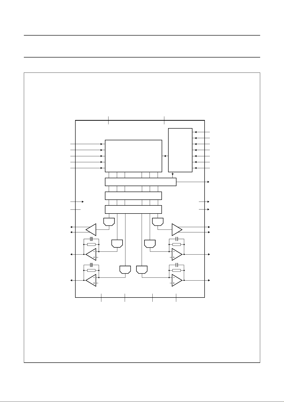
6 BLOCK DIAGRAM
handbook, full pagewidth
BCK
WS
DATAI12
DATAI34
DATAI56
TEST1
SYSCLK
VOUT1P
VOUT1N
DAC
DAC
V
SSD
CONTROL
INTERFACE
23
24
25
18
19
17
26
22
32
31
9
8
STATIC
MUTE
DEEM1
DEEM0
L3CLOCK
L3DATA
L3MODE
DS
TEST3
TEST2
VOUT2P
VOUT2N
V
DDD
21 20
UDA1328T
10
11
12
13
14
27
16
28
29
6-CHANNEL NOISE SHAPER
DAC
DIGITAL
INTERFACE
VOLUME/MUTE/DE-EMPHASIS
INTERPOLATION FILTER
DAC
VOUT3
VOUT5
1
DAC DAC
4
7, 15
n.c.
V
6
DDA
Fig.1 Block diagram.
1999 Oct 12 5
V
SSA
2
VOUT4
5
VOUT6
3
30
V
ref
MGR979
Page 6
Philips Semiconductors Preliminary specification
Multi-channel filter DAC UDA1328T
7 PINNING
SYMBOL PIN DESCRIPTION
VOUT3 1 channel 3 analog output
VOUT4 2 channel 4 analog output
V
SSA
VOUT5 4 channel 5 analog output
VOUT6 5 channel 6 analog output
V
DDA
n.c. 7 not connected (reserved)
TEST3 8 test output 3
STATIC 9 static mode/L3 mode switch input
BCK 10 bit clock input
WS 11 word select input
DATAI12 12 data input channel 1 and 2
DATAI34 13 data input channel 3 and 4
DATAI56 14 data input channel 5 and 6
n.c. 15 not connected (reserved)
SYSCLK 16 system clock: 256f
L3MODE 17 L3 mode selection input
L3CLOCK 18 L3 clock input
L3DATA 19 L3 data input
V
SSD
V
DDD
TEST2 22 test output 2
MUTE 23 static mute control input
DEEM1 24 DEEM control 1 input
DEEM0 25 L3 address select
DS 26 digital silence detect output
TEST1 27 test input 1
VOUT1P 28 channel 1 analog output P
VOUT1N 29 channel 1 analog output N
V
ref
VOUT2N 31 channel 2 analog output N
VOUT2P 32 channel 2 analog output P
3 analog ground
6 analog supply voltage
, 384fs,
s
512fsand 768f
s
20 digital ground
21 digital supply voltage
(static mode)
(L3 mode)/DEEM control 0 input
(static mode)
30 DAC reference voltage
handbook, halfpage
VOUT3
VOUT4
VOUT5
VOUT6
STATIC
DATAI12
DATAI34
DATAI56
SYSCLK
V
SSA
V
DDA
n.c.
TEST3
BCK
WS
n.c.
1
2
3
4
5
6
7
8
9
10
11
12
13
14
15
16
UDA1328T
Fig.2 Pin configuration.
MGR980
32
31
30
29
28
27
26
25
24
23
22
21
20
19
18
17
VOUT2P
VOUT2N
V
ref
VOUT1N
VOUT1P
TEST1
DS
DEEM0
DEEM1
MUTE
TEST2
V
DDD
V
SSD
L3DATA
L3CLOCK
L3MODE
1999 Oct 12 6
Page 7
Philips Semiconductors Preliminary specification
Multi-channel filter DAC UDA1328T
8 FUNCTIONAL DESCRIPTION
8.1 System clock
The UDA1328 operates in slave mode only, this means
that in allapplications the system must provide the system
clock.The system frequency is selectable.Theoptionsare
256fs, 384fs, 512fsand 768fsfor the L3 modeand 256fsor
384fs for the static mode. The system clock must be
frequency-locked to the digital interface signals.
It should be noted that the UDA1328 can operate from
5 to 100 kHz sampling frequency (fs). However in 768f
s
mode the sampling frequency must be limited to 55 kHz.
8.2 Application modes
Operating mode can be set with the STATIC pin, either to
L3 mode (STATIC = LOW) or to the static mode
(STATIC = HIGH). See Table 1 for pin functions in the
static mode.
Table 1 Mode selection in the static mode
PIN L3 MODE STATIC MODE
L3CLOCK L3CLOCK clock select
L3MODE L3MODE SF1
L3DATA L3DATA SF0
MUTE X
DEEM1 X
(2)
(2)
(1)
(1)
MUTE
DEEM1
DEEM0 L3ADR DEEM0
Notes
1. SF1 and SF0 are the Serial Format inputs (2-bit).
2. X means that the pin has no function in this mode and
can best be connected to ground.
8.3 Interpolation filter (DAC)
8.4 Digital silence detection
The UDA1328 can detect digital silence conditions in
channels 1 to 6, and report this via the output pin DS. This
function is implemented to allow for external manipulation
of the audio signal in the absence of program material,
such as muting or recorder control.
An active LOW output is produced at the DS pin if the
channels selected via L3 or for allchannels in staticmode,
carries all zeroes for at least 9600 consecutive audio
samples (equals 200 ms for fs= 48 kHz). The DS pin is
also active LOW when the output is digitally muted either
via the L3 interface or via the STATIC pin.
In static mode all channels participate in thedigital silence
detection. In L3 mode control each channel can be set,
either to participate in the digital silence detection or not.
8.5 Noise shaper
The 3rd-order noise shaper operates at 128fs. It shifts
in-band quantization noise to frequencies well above the
audio band. This noise shaping technique enables high
signal-to-noise ratios to be achieved. The noise shaper
output is converted into an analog signal using a Filter
Stream DAC (FSDAC).
8.6 Filter stream DAC
The FSDAC is a semi-digital reconstruction filter that
converts the 1-bit data stream of the noise shaper to an
analog output voltage. The filter coefficients are
implemented as current sources and are summed at
virtual ground of the output operational amplifier. In this
way very high signal-to-noise performance and low clock
jitter sensitivity is achieved. No post-filter is neededdue to
the inherent filterfunction of the DAC. On-board amplifiers
convert the FSDAC output current to an output voltage
signal capable of driving a line output.
The digital filter interpolates from 1 to 128fs by cascading
a half-band filter and a FIR filter, see Table 2. The overall
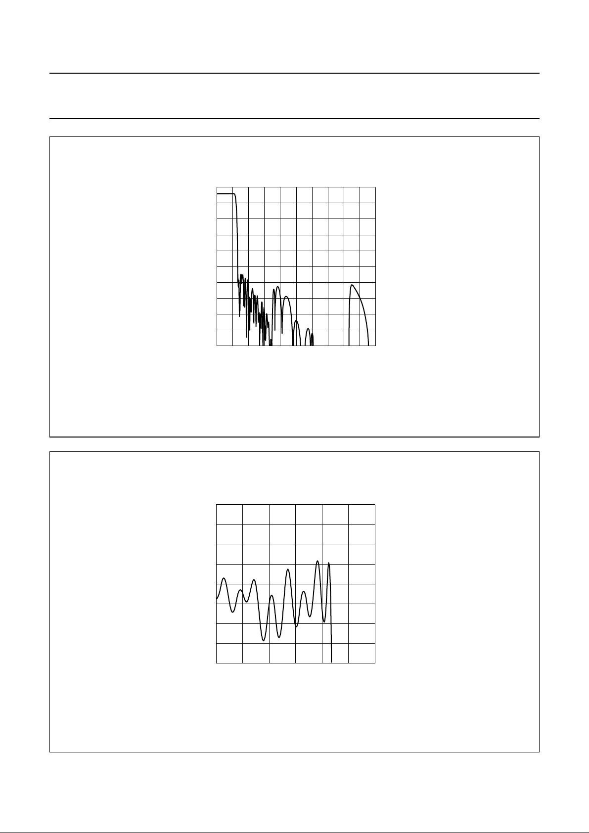
filter characteristic ofthe digital filters is illustrated in Fig.3,
andthe pass-band ripple isillustratedin Fig.4. Both figures
are with a 44.1 kHz sampling frequency.
Table 2 Interpolation filter characteristics
ITEM CONDITION VALUE (dB)
Pass-band ripple 0 to 0.45f
Stop band >0.55f
Dynamic range 0 to 0.45f
s
s
s
±0.02
−55
>114
DC gain −−3.5
1999 Oct 12 7
The output voltage of the FSDAC scales proportionally
with the power supply voltage.
8.7 Static mode
The UDA1328 is set to static mode by setting the STATIC
pin HIGH. The function of 6 pins of the device now get
another function as can be seen in Table 1.
8.7.1 SYSTEM CLOCK SETTING
In static mode pin 18 (L3CLOCK) is used to select the
system clock setting.When pin 18 is LOW, the device isin
256fs mode, when pin 18 is HIGH the device is in 384f
s
mode.
Page 8
Philips Semiconductors Preliminary specification
Multi-channel filter DAC UDA1328T
8.7.2 DE-EMPHASIS CONTROL
Instaticpin mode the pinsDEEM0 and DEEM1controlthe
de-emphasis mode; see Table 3.
Table 3 De-emphasis control
DEEM MODE DEEM1 DEEM0
No de-emphasis 0 0
32 kHz de-emphasis 0 1
44.1 kHz de-emphasis 1 0
48 kHz de-emphasis 1 1
8.7.3 DIGITAL INTERFACE FORMATS
Instaticpin mode the digitalaudiointerfaceformats can be
selected via pin 17 (SF1) and 19 (SF0). The following
interface formats can be selected (see also Table 4):
• I2S-bus with data word length of up to 24 bits
• LSB-justified format with data word length of
16, 20 or 24 bits.
Table 4 Input format selection in the static mode
INPUT FORMAT SF1 SF0
2
I
S-bus 0 0
LSB-justified 16 bits 0 1
LSB-justified 20 bits 1 0
LSB-justified 24 bits 1 1
8.8 L3 mode
The device is set to L3 mode by setting the STATIC pin to
LOW. The device can then be controlled via the L3
microcontroller interface (see Chapter 9).
8.8.1 DIGITAL INTERFACE FORMATS
The following interface formats can be selected in the
L3 mode:
• I2S-bus with data word length of up to 24 bits
• MSB-justified with data word length of up to 24 bits
• LSB-justified format with data word length of 16, 18,
20 or 24 bits.
8.8.2 L3 ADDRESS
TheUDA1328canbe addressed via the L3 microcontroller
interface using oneof two addresses.This is done in order
to individually control the UDA1328 and other Philips
DACs or CODECs via the same L3 bus.
The address can be selected using pin 25 (DEEM0) in
L3 mode.When pin 25 isset LOW, theaddress is 000100.
When pin 25 is set HIGH the address is 000101.
It should be noted that thedigital audio interfaceholds that
the BCK frequency can be 64 times the WS maximum
frequency, or f
BCK
≤ 64 × f
WS
1999 Oct 12 8
Page 9
Philips Semiconductors Preliminary specification
Multi-channel filter DAC UDA1328T
fs= 6.14400 MHz
handbook, halfpage
0
volume
(dB)
−20
−40
−60
−80
−100
0 200
Fig.3 Overall frequency characteristics.
MGR981
40 80 120 160
f (kHz)
−3.45
handbook, halfpage
V
o
(dB)
−3.47
−3.49
−3.51
−3.53
0 102030
fs= 6.14400 MHz
Fig.4 Pass-band ripple of all filters.
1999 Oct 12 9
MGR982
f (kHz)
Page 10

This text is here in white to force landscape pages to be rotated correctly when browsing through the pdf in the Acrobat reader.This text is here in
a
_white to force landscape pages to be rotated correctly when browsing through the pdf in the Acrobat reader.This text is here inThis text is here in
white to force landscape pages to be rotated correctly when browsing through the pdf in the Acrobat reader. white to force landscape pages to be ...
1999 Oct 12 10
ndbook, full pagewidth
Philips Semiconductors Preliminary specification
Multi-channel filter DAC UDA1328T
WS
BCK
DATA
WS
BCK
DATA
WS
BCK
DATA
WS
BCK
MSB B2
LEFT
INPUT FORMAT I
LEFT
LEFT
MSB B2 B3 B4
LEFT
21> = 812 3
MSB MSBB2
RIGHT
3
2
S
16
15 2 1
MSB
B2
16
1518 17 2 1
16
1518 1720 19 2 1
> = 8
B15
LSB
LSB JUSTIFIED FORMAT 16 BITS
B17
LSB
LSB JUSTIFIED FORMAT 18 BITS
RIGHT
RIGHT
RIGHT
16
MSB B2
16 1518 17 2 1
MSB B2 B3 B4
16
15 2 1
B15 LSB
B17 LSB
1518 1720 19 2 1
DATA
WS
BCK
DATA
MSB
B19
B23
LSB
LSB
MSB
MSB B2 B3 B4 B5 B6
RIGHT
16
1518 1720 1922 212324 21
B2
B3 B4
B5 B6 B7 B8 B9 B10
MSB B2 B3 B4 B5 B6
LSB JUSTIFIED FORMAT 20 BITS
LEFT
16
1518 1720 1922 212324 2 1
B2
B3 B4
B5 B6 B7 B8 B9 B10
LSB JUSTIFIED FORMAT 24 BITS
B19 LSB
B23 LSB
MGR751
Fig.5 Serial interface; input formats.
Page 11

Philips Semiconductors Preliminary specification
Multi-channel filter DAC UDA1328T
9 L3 INTERFACE DESCRIPTION
The following system and digital sound processing
features can be controlled in the microcontroller mode of
the UDA1328:
• Data input format
• De-emphasis for 32, 44.1, 48 and 96 kHz
• Volume control: master and for individual channels
• Soft or quick mute: master and for individual channels
• Output polarity control: master and for individual
channels
• Digital silence control: master and for individual
channels
• Power-down mode.
Theexchange of dataand control information betweenthe
microcontroller and the UDA1328 is accomplished via a
serial hardware interface comprising the following pins:
L3DATA: microcontroller interface data line
L3MODE: microcontroller interface mode line
L3CLOCK: microcontroller interface clock line.
Information transfer via the microcontroller bus is
organized LSB firstand is in accordance with the socalled
‘L3’ format, in which two different modes of operation can
be distinguished. The address mode and data transfer
mode are illustrated in Figs 6 and 7.
The address mode is required to select a device
communicating via the L3-bus and to define the
destination registers for the data transfer mode. Data
transfer for the UDA1328 can only be in one direction;
inputto the UDA1328 toprogramits sound processing and
other functional features.
9.1 Address mode
The address mode is used to select a device for
subsequent data transfer and to define the destination
registers. The address mode is characterizedby L3MODE
being LOW and a burst of 8 pulses on L3CLOCK,
accompanied by 8 data bits. The fundamental timing is
shown in Fig.6. Data bits 0 and 1 indicate the type of
subsequent data transfer as given in Table 5.
Table 5 Selection of data transfer
BIT 1 BIT 0 TRANSFER
0 0 data (volume, de-emphasis, mute,
digital silence mode, polarity control)
0 1 not used
1 0 status (system clock frequency,
data input format, mute mode,
power control)
1 1 not used
Data bits 7 to 2 represent a 6-bit deviceaddress, with bit 7
being the MSB and bit 2 the LSB. The address of the
UDA1328 is 000100 (bit 7 to bit 2) when L3ADR
(DEEM0) = LOW or 000101 when L3ADR = HIGH. In the
eventthat the UDA1328receivesa different address, itwill
deselect its microcontroller interface logic.
9.2 Data transfer mode
The selection preformed in the address mode remains
active during subsequent data transfers, until the
UDA1328 receives a new address command. The
fundamental timing of data transfers is essentially the
same as in the address mode, shown in Fig.6. The
maximuminputclockand data rate is 64fs.All transfersare
byte wise, i.e. they are based on groups of 8 bits. Data will
be stored in the UDA1328 after the eighth bit of a byte has
been received. A multibyte transfer is illustrated in Fig.8.
9.2.1 PROGRAMMING THE SOUND PROCESSING AND
OTHER FEATURES
The sound processing and other feature values are stored
inindependent registers. The first selectionoftheregisters
is achieved by the choice of data type that is transferred.
This is performed in the address mode, bit 1 and bit 0
(see Table 5). The second selection is performed by the
2 MSBs of the data byte (bit 7 and bit 6). The other bits in
thedata byte (bit 5 to bit 0) isthe value that isplaced in the
selected registers.
When the data transfer of type ‘data’ is selected, the
features volume, sub volume, de-emphasis, mute, digital
silence settings, output polarity control and channel
selection can be controlled. When thedata transfer oftype
‘status’ is selected, the features system clock frequency,
data input format, mute mode and power control can be
controlled.
1999 Oct 12 11
Page 12

Philips Semiconductors Preliminary specification
Multi-channel filter DAC UDA1328T
handbook, full pagewidth
L3MODE
L3CLOCK
L3DATA
t
h(L3)A
t
CLK(L3)L
t
su(L3)DA
t
CLK(L3)H
t
BIT 0
su(L3)A
Fig.6 Timing address mode.
t
h(L3)DA
t
su(L3)A
t
h(L3)A
T
cy(CLK)(L3)
BIT 7
MGL723
t
t
su(L3)D
stp(L3)
t
h(L3)DA
BIT 0
t
CLK(L3)H
t
CLK(L3)L
handbook, full pagewidth
L3MODE
L3CLOCK
L3DATA
write
Fig.7 Timing for data transfer mode.
1999 Oct 12 12
t
su(L3)DA
T
cy(CLK)L3
t
t
h(L3)DA
BIT 7
h(L3)D
t
stp(L3)
MGL724
Page 13

Philips Semiconductors Preliminary specification
Multi-channel filter DAC UDA1328T
t
handbook, full pagewidth
L3MODE
L3CLOCK
L3DATA
stp(L3)
address
addressdata byte #1 data byte #2
MGL725
Fig.8 Multibyte transfer.
Table 6 Data transfer of type ‘status’
BIT 7 BIT 6 BIT 5 BIT 4 BIT 3 BIT 2 BIT 1 BIT 0 REGISTER SELECTED
0 RST SC1 SC0 IF2 IF1 IF0 0 ReSeT
System Clock frequency (1 and 0)
data Input Format (2 to 0)
100000QMPCQuick/soft Mute
Power Control
Table 7 Data transfer of type ‘data’
BIT 7 BIT 6 BIT 5 BIT 4 BIT 3 BIT 2 BIT 1 BIT 0 REGISTER SELECTED
0 0 VC5 VC4 VC3 VC2 VC1 VC0 Volume Control (5 to 0)
010000VQ1VQ00.25 dB step sub volume (1 and 0)
1 0 DE2 DE1 DE0 MT DSM PLC DE-emphasis (2 to 0)
MuTe
Digital Silence Mode
PoLarity Control
1100ACHCH2CH1CH0All CHannels select
CHannel select (2 to 0)
1999 Oct 12 13
Page 14

Philips Semiconductors Preliminary specification
Multi-channel filter DAC UDA1328T
9.2.2 RESET BIT
A 1-bit value to initialize the L3 registers with the default
settings (except the system clock setting and the data
input format setting) by writing a logic 1 to RST
(see Table 6).
The default settings after reset are as follows:
• Mute mode: soft mute
• Power: on
• Volume: 0 dB
• Sub volume: 0 dB
• De-emphasis: off
• Mute: off
• Silence detect mode: detect
• Polarity: non-inverting.
9.2.3 SYSTEM CLOCK FREQUENCY
A 2-bit value (SC1 and SC0) to select the used external
clock frequency (see Table 8).
Table 8 System clock frequency settings
SC1 SC0 FUNCTION
0 0 512f
0 1 384f
1 0 256f
1 1 768f
s
s
s
s
9.2.4 DATA INPUT FORMAT
A 3-bit value (IF2 to IF0) to select the used data format
(see Table 9).
Table 9 Data input format settings
IF2 IF1 IF0 FUNCTION
000I
2
S-bus
0 0 1 LSB-justified; 16 bits
0 1 0 LSB-justified; 18 bits
0 1 1 LSB-justified; 20 bits
1 0 0 MSB-justified
1 0 1 LSB-justified; 24 bits
1 1 0 reserved
1 1 1 reserved
9.2.5 QUICK MUTE
A 1-bit value to set the mute mode to either soft mute (via
cosine roll-off), quick or hard mute.
Table 10 Quick mute
QM FUNCTION
0 soft mute mode
1 quick mute mode
9.2.6 POWER CONTROL
A 1-bit value to disable the ADC and/or DAC to reduce
power consumption.
Table 11 Power control settings
PC FUNCTION
0 all channels off
1 all channels on
9.3 Feature settings
In the UDA1328 there are features that can be controlled
either per-channel or all at the same time. These features
are:
• Volume control
• Sub volume control
• Mute
• Output polarity control
• Digital silence detect.
Whena ‘per-channel’ setting is requiredforthese features,
the ACH bit (see Table 7) must be set to logic 0 before
writing a new value to one of the features. Once this has
been performed a channel is selected via the CH2 to CH0
bits.Thefeaturesforthis channel can be controlled without
sending the same channel address again (low
microcontroller mode).
When the ACH bit is set to logic 1, which means ‘all
channels select’, all channels will be set to thesame value
of the feature sent afterwards.
For the digital silence detector it holds that the DS pin is
either active on the selected channel when bit ACH is set
to logic 0 before writing the DSM bit, or the DS pin is active
on all channels when the ACH bit is set to logic 1.
1999 Oct 12 14
Page 15

Philips Semiconductors Preliminary specification
Multi-channel filter DAC UDA1328T
9.3.1 CHANNEL SELECTION MODE
A 1-bit value to set the selection mode (either individually
or per-channel) for the volume, mute, polarity control and
silence detect isgiven in Table 12. The 3-bit value isgiven
in Table 13.
Table 12 1-bit selection
(1)
ACH
0 individual channel select; use CH(2 : 0)
1 all channels selected
Note
1. For setting the de-emphasis mode, the ACH bit must
be set to logic 1 before setting the de-emphasis.
Table 13 3-bit selection
CH2 CH1 CH0 FUNCTION
0 0 0 channel 1 selected
0 0 1 channel 2 selected
0 1 0 channel 3 selected
0 1 1 channel 4 selected
1 0 0 channel 5 selected
1 0 1 channel 6 selected
1 1 0 not used
1 1 1 not used
9.3.2 VOLUME CONTROL
A 6-bit value to program the channel volume attenuation
(VC5 to VC0). The range is 0 dB to −∞ dB in steps of 1 dB
(see Table 14).
FUNCTION
9.3.3 SUB VOLUME CONTROL
A 2-bit value to program the channel volume attenuation
with a 0.25 dB step (VQ1 and VQ0). To validate the sub
volume settings in these registers, the volume control
registers of corresponding channels must be updated one
after the other.
Table 15 Sub volume settings
VQ1 VQ0 VOLUME (dB)
0 0 0.00
01−0.25
10−0.50
11−0.75
9.3.4 MUTE
A 1-bit value to enable the digital mute (the type of mute is
set via the QM bit in the status register).
Table 16 Mute
MT FUNCTION
0 no muting
1 muting
9.3.5 DIGITAL SILENCE MODE
A 1-bit value to set the digital silence mode. This bit is set
together with the channel address CH2 to CH0 and the
ACH bit.
When the ACH bit is set to logic 0, each channel can be
selected for digital silence detection. When the ACH bit is
set to logic 1 all channels are selected.
Table 14 Volume settings
VC5 VC4 VC3 VC2 VC1 VC0 VOLUME (dB)
000000 0
000001 0
000010 −1
000011 −2
:::::: :
111011 −58
111100 −59
111101 −60
111110 −∞
111111 −∞
1999 Oct 12 15
Table 17 Digital silence mode
DSM FUNCTION
0 no participation
1 participates
Page 16

Philips Semiconductors Preliminary specification
Multi-channel filter DAC UDA1328T
9.3.6 DE-EMPHASIS
A 2-bit value to enable the digital de-emphasis filter.
9.3.7 OUTPUT POLARITY CONTROL
A 1-bit value to program the output polarity of the output
signal.This bit must beusedtogether with the CH2 to CH0
Table 18 De-emphasis settings
DE2 DE1 DE0 FUNCTION
0 0 0 no de-emphasis
0 0 1 de-emphasis; 32 kHz
0 1 0 de-emphasis; 44.1 kHz
0 1 1 de-emphasis; 48 kHz
bits and the ACH bit to either select the polarity for all
channels or to set for each channel individually.
Table 19 Output polarity control
PLC FUNCTION
0 non-inverting
1 inverting
1 0 0 de-emphasis; 96 kHz
10 LIMITING VALUES
In accordance with the Absolute Maximum Rating System (IEC 134).
SYMBOL PARAMETER CONDITIONS MIN. MAX. UNIT
V
DDD
V
DDA
T
xtal(max)
T
stg
T
amb
V
es
digital supply voltage note 1 − 5.0 V
analog supply voltage note 1 − 5.0 V
maximum crystal temperature − 150 °C
storage temperature −65 +125 °C
ambient temperature −20 +85 °C
electrostatic handling note 2 −3000 +3000 V
note 3 −250 +250 V
Notes
1. All supply connections must be made to the same power supply.
2. Equivalent to discharging a 100 pF capacitor via a 1.5 kΩ series resistor, expect pin 19 (L3DATA) which can
withstand ESD pulses of −2500 to +2500 V.
3. Equivalent to discharging a 200 pF capacitor via a 0.75 µH series inductor.
11 HANDLING
Inputs and outputs are protected against electrostatic discharge in normal handling. However, to be totally safe, it is
desirable to take normal precautions appropriate to handling MOS devices.
12 THERMAL CHARACTERISTICS
SYMBOL PARAMETER CONDITIONS VALUE UNIT
R
th(j-a)
thermal resistance from junction to ambient in free air 58 K/W
13 QUALITY SPECIFICATION
In accordance with
Handbook”
.
“SNW-FQ-611-E”
. The number of the quality specification can be found in the
“Quality Reference
1999 Oct 12 16
Page 17

Philips Semiconductors Preliminary specification
Multi-channel filter DAC UDA1328T
14 DC CHARACTERISTICS
V
DDD=VDDA
specified.
SYMBOL PARAMETER CONDITIONS MIN. TYP. MAX. UNIT
Supplies
V
DDA
V
DDD
I
DDA
I
DDD
Digital input pins: 5 V tolerant TTL compatible
V
IH
V
IL
V
IL(th)
V
IH(th)
V
hyst
I
input leakage current −−1µA
LI
C
i
Digital output pin
V
OH
V
OL
DAC
V
ref
I
o(max)
R
L
C
L
= 3.3 V; T
=25°C; RL=5kΩ. All voltages referenced to ground (pins 3 and 20); unless otherwise
amb
analog supply voltage note 1 2.7 3.3 3.6 V
digital supply voltage note 1 2.7 3.3 3.6 V
analog supply current all channels active;
− 28 − mA
operating mode
digital supply current operating mode − 11 − mA
HIGH-level input voltage 2.0 −−V
LOW-level input voltage −−0.8 V
LOW-levelthreshold input voltage;
0.9 − 1.45 V
falling edge
HIGH-level threshold input
1.4 − 1.9 V
voltage; rising edge
Schmitt trigger hysteresis voltage 0.4 − 0.7 V
input capacitance −−10 pF
HIGH-level output voltage IOH= −2 mA 0.85V
−−V
DDD
LOW-level output voltage IOL=2mA −−0.4 V
reference voltage referenced to V
SSA
0.45V
DDA
0.5V
DDA
0.55V
DDA
V
maximum output current (THD + N)/S < 0.1% − 0.22 − mA
load resistance 3 −−kΩ
load capacitance note 2 −−50 pF
Notes
1. All supply connections must be made to the same external power supply unit.
2. When the DAC drives a capacitive load above 50 pF, a series resistor of 100 Ω must be used to prevent oscillations
in the output operational amplifier.
1999 Oct 12 17
Page 18

Philips Semiconductors Preliminary specification
Multi-channel filter DAC UDA1328T
15 AC CHARACTERISTICS (ANALOG)
V
DDD=VDDA
otherwise specified.
SYMBOL PARAMETER CONDITIONS MIN. TYP. MAX. UNIT
DAC: channels 1 and 2 in differential mode
V
o(rms)
∆V
o
(THD + N)/S total harmonic distortion plus
S/N signal-to-noise ratio f
DAC: channels 3 to 6
V
o(rms)
∆V
o
(THD + N)/S total harmonic distortion plus
S/N signal-to-noise ratio f
PSRR power supply rejection ratio f
= 3.3 V; fi= 1 kHz; T
=25°C; RL=5kΩ. All voltages referenced to ground (pins 3 and 20); unless
amb
output voltage (RMS value) − 2 − V
unbalance between channels − 0.1 − dB
f
= 48 kHz; at 0 dB −−95 −88 dB
s
noise-to-signal ratio
= 48 kHz; at −60 dB; A-weighted −−46 − dB
f
s
f
= 96 kHz; at 0 dB −−90 − dB
s
f
= 96 kHz; at −60 dB; A-weighted −−44 − dB
s
= 48 kHz; code = 0; A-weighted − 106 − dB
s
f
= 96 kHz; code = 0; A-weighted − 104 − dB
s
output voltage (RMS value) − 1 − V
unbalance between channels − 0.1 − dB
f
= 48 kHz; at 0 dB −−90 −83 dB
s
noise-to-signal ratio
f
= 48 kHz; at −60 dB; A-weighted −−43 − dB
s
f
= 96 kHz; at 0 dB −−85 − dB
s
= 96 kHz; at −60 dB; A-weighted −−41 − dB
f
s
= 48 kHz; code = 0; A-weighted − 103 − dB
s
f
= 96 kHz; code = 0; A-weighted − 101 − dB
s
ripple
= 1 kHz; V
ripple(p-p)
= 100 mV − 50 − dB
1999 Oct 12 18
Page 19

Philips Semiconductors Preliminary specification
Multi-channel filter DAC UDA1328T
16 AC CHARACTERISTICS (DIGITAL)
V
DDD=VDDA
otherwise specified. The typical timing is specified at 44.1 kHz sampling frequency.
SYMBOL PARAMETER CONDITIONS MIN. TYP. MAX. UNIT
T
sys
t
CWL
t
CWH
t
r
t
f
Serial input data timing (see Fig.9)
T
cy(CLK)(bit)
t
CLKH(bit)
t
CLKL(bit)
t
r
t
f
t
su(i)(D)
t
h(i)(D)
t
su(WS)
t
h(WS)
Microcontroller interface timing (see Figs 6, 7 and 8)
T
cy(CLK)(L3)
t
CLK(L3)H
t
CLK(L3)L
t
su(L3)A
t
h(L3)A
t
su(L3)D
t
h(L3)D
t
su(L3)DA
t
h(L3)DA
t
stp(L3)
= 2.7 to 3.6 V; T
system clock cycle f
LOW-level system clock pulse
width
HIGH-level system clock pulse
width
= −20 to +85 °C; RL=5kΩ. All voltages referenced to ground (pins 3 and 20); unless
amb
= 256f
f
f
f
f
f
f
f
sys
sys
sys
sys
sys
sys
sys
sys
s
= 384f
s
= 512f
s
= 768fs; note 1 20 30 260 ns
< 19.2 MHz 30 − 70 %T
≥ 19.2 MHz 40 − 60 %T
< 19.2 MHz 30 − 70 %T
≥ 19.2 MHz 40 − 60 %T
35 88 780 ns
23 59 520 ns
20 44 390 ns
rise time −−20 ns
fall time −−20 ns
bit clock period 140 −−ns
bit clock HIGH time 60 −−ns
bit clock LOW time 60 −−ns
rise time −−20 ns
fall time −−20 ns
data input set-up time 20 −−ns
data input hold time 0 −−ns
word selection set-up time 20 −−ns
word selection hold time 10 −−ns
L3CLOCK time 500 −−ns
L3CLOCK HIGH time 250 −−ns
L3CLOCK LOW time 250 −−ns
L3MODE set-up time addressing mode 190 −−ns
L3MODE hold time addressing mode 190 −−ns
L3MODE set-up time data transfer mode 190 −−ns
L3MODE hold time data transfer mode 190 −−ns
L3DATA set-up time data transfer and addressing mode 190 −−ns
L3DATA hold time data transfer and addressing mode 30 −−ns
L3MODE halt time 190 −−ns
sys
sys
sys
sys
Note
1. In the 768f
clock mode, the sampling frequency must be limited to 55 kHz.
s
1999 Oct 12 19
Page 20

Philips Semiconductors Preliminary specification
Multi-channel filter DAC UDA1328T
handbook, full pagewidth
WS
BCK
DATAI
t
r
t
CLKH(bit)
t
CLKL(bit)
T
cy(CLK)(bit)
t
h(WS)
t
t
f
su(WS)
t
su(i)(D)
t
h(i)(D)
MGL721
Fig.9 Serial interface timing.
handbook, full pagewidth
t
CWH
t
CWL
T
sys
Fig.10 System clock timing.
1999 Oct 12 20
MGR984
Page 21

Philips Semiconductors Preliminary specification
Multi-channel filter DAC UDA1328T
17 APPLICATION INFORMATION
handbook, full pagewidth
VOUT3
AGND
VOUT4
AGND
VOUT5
AGND
VOUT6
AGND
R13 100 Ω
R14 10 kΩ
R15 100 Ω
R16 10 kΩ
R17 100 Ω
R18 10 kΩ
R19 100 Ω
R20 10 kΩ
V
DDA
AGND
1 Ω
C7 47 µF
(16 V)
C8 47 µF
(16 V)
C9 47 µF
(16 V)
C10 47 µF
(16 V)
100 µF
(16 V)
STATIC/L3
VOUT3
VOUT4
V
VOUT5
VOUT6
100 nF
V
n.c.
TEST3
STATIC
SSA
DDA
BCK
WS
1
2
3
4
5
6
7
8
UDA1328T
9
10
11
32
31
30
29
28
27
26
25
24
23
22
VOUT2P
VOUT2N
V
ref
C14
100 nF
VOUT1N
VOUT1P
TEST1
DS
DEEM0
DEEM1
MUTE
TEST2
AGND
10 kΩ
10 kΩ
C13
47 µF
(16 V)
10 kΩ
10 kΩ
3.3 V
AGND
AGND
10 kΩ
5
6
100 pF
10 kΩ
10 kΩ
100 pF
2
3
10 kΩ
BZN32A07
ground
1/2
NE5532
7
1
1/2
NE5532
100 µF
(16 V)
47 µF
(16 V)
47 µF
(16 V)
AGND
AGND
AGND
DGND
DGNDAGND
100 Ω
10 kΩ
100 Ω
10 kΩ
100 µF
(16 V)
V
V
DDA
DDD
VOUT2
VOUT1
SYSCLK
47 Ω
DATAI12
DATAI34
DATAI56
n.c.
SYSCLK
12
13
14
15
16
Fig.11 Application diagram.
1999 Oct 12 21
21
20
19
18
17
V
DDD
V
SSD
L3DATA
L3CLOCK
L3MODE
100
nF
MGR983
1 Ω
100 µF
(16 V)
DGND
V
DDD
Page 22

Philips Semiconductors Preliminary specification
Multi-channel filter DAC UDA1328T
18 PACKAGE OUTLINE
SO32: plastic small outline package; 32 leads; body width 7.5 mm
SOT287-1
D
c
y
Z
32
pin 1 index
1
e
17
A
2
A
16
w M
b
p
E
H
E
1
L
detail X
A
X
v M
A
Q
(A )
L
p
A
3
θ
0 5 10 mm
scale
DIMENSIONS (inch dimensions are derived from the original mm dimensions)
UNIT
mm
inches
Note
1. Plastic or metal protrusions of 0.15 mm maximum per side are not included.
A
max.
2.65
0.10
OUTLINE
VERSION
SOT287-1
A1A
0.3
0.1
0.012
0.004
A3b
0.49
0.36
0.02
0.01
p
0.27
0.18
0.011
0.007
2
2.45
0.25
2.25
0.096
0.01
0.086
IEC JEDEC EIAJ
(1)E(1)
cD
20.7
20.3
0.81
0.80
REFERENCES
7.6
7.4
0.30
0.29
1.27
0.050
1999 Oct 12 22
eHELLpQZywv θ
10.65
10.00
0.419
0.394
1.4
0.055
1.1
0.4
0.043
0.016
1.2
1.0
0.047
0.039
0.25 0.1
0.25
0.010.01
EUROPEAN
PROJECTION
0.004
(1)
0.95
0.55
0.037
0.022
ISSUE DATE
95-01-25
97-05-22
o
8
o
0
Page 23

Philips Semiconductors Preliminary specification
Multi-channel filter DAC UDA1328T
19 SOLDERING
19.1 Introduction to soldering surface mount
packages
Thistextgives a very briefinsighttoa complex technology.
A more in-depth account of soldering ICs can be found in
our
“Data Handbook IC26; Integrated Circuit Packages”
(document order number 9398 652 90011).
There is no soldering method that is ideal for all surface
mount IC packages. Wave soldering isnot always suitable
for surface mount ICs, or for printed-circuit boards with
high population densities. In these situations reflow
soldering is often used.
19.2 Reflow soldering
Reflow soldering requires solder paste (a suspension of
fine solder particles, flux and binding agent) to be applied
tothe printed-circuit board byscreen printing, stencilling or
pressure-syringe dispensing before package placement.
Several methods exist for reflowing; for example,
infrared/convection heating in a conveyor type oven.
Throughput times (preheating,soldering and cooling) vary
between 100 and 200 seconds depending on heating
method.
Typical reflow peak temperatures range from
215 to 250 °C. The top-surface temperature of the
packages should preferable be kept below 230 °C.
If wave soldering is used the following conditions must be
observed for optimal results:
• Use a double-wave soldering method comprising a
turbulent wave with high upward pressure followed by a
smooth laminar wave.
• For packages with leads on two sides and a pitch (e):
– larger than or equal to 1.27 mm, the footprint
longitudinal axis is preferred to be parallel to the
transport direction of the printed-circuit board;
– smaller than 1.27 mm, the footprint longitudinal axis
must be parallel to the transport direction of the
printed-circuit board.
The footprint must incorporate solder thieves at the
downstream end.
• Forpackageswith leads on four sides,thefootprintmust
be placed at a 45° angle to the transport direction of the
printed-circuit board. The footprint must incorporate
solder thieves downstream and at the side corners.
During placement andbefore soldering, the package must
be fixed with a droplet of adhesive. The adhesive can be
applied by screen printing, pin transfer or syringe
dispensing. The package can be soldered after the
adhesive is cured.
Typical dwell time is 4 seconds at 250 °C.
A mildly-activated flux will eliminate the need for removal
of corrosive residues in most applications.
19.3 Wave soldering
Conventional single wave soldering is not recommended
forsurfacemount devices (SMDs) or printed-circuitboards
with a high component density, as solder bridging and
non-wetting can present major problems.
To overcome these problems the double-wave soldering
method was specifically developed.
1999 Oct 12 23
19.4 Manual soldering
Fix the component by first soldering two
diagonally-opposite end leads. Use a low voltage (24 V or
less) soldering iron applied to the flat part of the lead.
Contact time must be limited to 10 seconds at up to
300 °C.
When using a dedicated tool, all other leads can be
soldered in one operation within 2 to 5 seconds between
270 and 320 °C.
Page 24

Philips Semiconductors Preliminary specification
Multi-channel filter DAC UDA1328T
19.5 Suitability of surface mount IC packages for wave and reflow soldering methods
PACKAGE
WAVE REFLOW
(1)
BGA, LFBGA, SQFP, TFBGA not suitable suitable
SOLDERING METHOD
HBCC, HLQFP, HSQFP, HSOP, HTQFP, HTSSOP, SMS not suitable
(3)
PLCC
, SO, SOJ suitable suitable
LQFP, QFP, TQFP not recommended
SSOP, TSSOP, VSO not recommended
(2)
(3)(4)
(5)
suitable
suitable
suitable
Notes
1. All surface mount (SMD) packages are moisture sensitive. Depending upon the moisture content, the maximum
temperature (with respect to time) and body size of the package, there is a risk that internal or external package
cracks may occur due to vaporization of the moisture in them (the so called popcorn effect). For details, refer to the
Drypack information in the
“Data Handbook IC26; Integrated Circuit Packages; Section: Packing Methods”
.
2. These packages are not suitable for wave soldering as a solder joint between the printed-circuit board and heatsink
(at bottom version) can not be achieved, and as solder may stick to the heatsink (on top version).
3. If wave soldering is considered, then the package must be placed at a 45° angle to the solder wave direction.
The package footprint must incorporate solder thieves downstream and at the side corners.
4. Wave soldering is only suitable for LQFP, TQFP and QFP packages with a pitch (e) equal to or larger than 0.8 mm;
it is definitely not suitable for packages with a pitch (e) equal to or smaller than 0.65 mm.
5. Wave soldering is only suitable for SSOP and TSSOP packages with a pitch (e)equal toor larger than 0.65 mm; it is
definitely not suitable for packages with a pitch (e) equal to or smaller than 0.5 mm.
20 DEFINITIONS
Data sheet status
Objective specification This data sheet contains target or goal specifications for product development.
Preliminary specification This data sheet contains preliminary data; supplementary data may be published later.
Product specification This data sheet contains final product specifications.
Limiting values
Limiting values given are in accordance with the Absolute Maximum Rating System (IEC 134). Stress above one or
more of the limiting values may cause permanent damage to the device. These are stress ratings only and operation
of the device at these or at any other conditions above those given in the Characteristics sections of the specification
is not implied. Exposure to limiting values for extended periods may affect device reliability.
Application information
Where application information is given, it is advisory and does not form part of the specification.
21 LIFE SUPPORT APPLICATIONS
These products are not designed for use in life support appliances, devices, or systems where malfunction of these
products can reasonably be expected to result in personal injury. Philips customers using or selling these products for
use in such applications do so at their own risk and agree to fully indemnify Philips for any damages resulting from such
improper use or sale.
1999 Oct 12 24
Page 25

Philips Semiconductors Preliminary specification
Multi-channel filter DAC UDA1328T
NOTES
1999 Oct 12 25
Page 26

Philips Semiconductors Preliminary specification
Multi-channel filter DAC UDA1328T
NOTES
1999 Oct 12 26
Page 27

Philips Semiconductors Preliminary specification
Multi-channel filter DAC UDA1328T
NOTES
1999 Oct 12 27
Page 28

Philips Semiconductors – a w orldwide compan y
Argentina: see South America
Australia: 3 Figtree Drive, HOMEBUSH, NSW 2140,
Tel. +61 2 9704 8141, Fax. +61 2 9704 8139
Austria: Computerstr. 6, A-1101 WIEN, P.O. Box 213,
Tel. +43 1 60 101 1248, Fax. +43 1 60 101 1210
Belarus: Hotel Minsk Business Center, Bld. 3, r. 1211, Volodarski Str. 6,
220050 MINSK, Tel. +375 172 20 0733, Fax. +375 172 20 0773
Belgium: see The Netherlands
Brazil: see South America
Bulgaria: Philips Bulgaria Ltd., Energoproject, 15th floor,
51 James Bourchier Blvd., 1407 SOFIA,
Tel. +359 2 68 9211, Fax. +359 2 68 9102
Canada: PHILIPS SEMICONDUCTORS/COMPONENTS,
Tel. +1 800 234 7381, Fax. +1 800 943 0087
China/Hong Kong: 501 Hong Kong Industrial Technology Centre,
72 Tat Chee Avenue, Kowloon Tong, HONG KONG,
Tel. +852 2319 7888, Fax. +852 2319 7700
Colombia: see South America
Czech Republic: see Austria
Denmark: Sydhavnsgade 23, 1780 COPENHAGEN V,
Tel. +45 33 29 3333, Fax. +45 33 29 3905
Finland: Sinikalliontie 3, FIN-02630 ESPOO,
Tel. +358 9 615 800, Fax. +358 9 6158 0920
France: 51 Rue Carnot, BP317, 92156 SURESNES Cedex,
Tel. +33 1 4099 6161, Fax. +33 1 4099 6427
Germany: Hammerbrookstraße 69, D-20097 HAMBURG,
Tel. +49 40 2353 60, Fax. +49 40 2353 6300
Hungary: see Austria
India: Philips INDIA Ltd, Band Box Building, 2nd floor,
254-D, Dr. Annie Besant Road, Worli, MUMBAI 400 025,
Tel. +91 22 493 8541, Fax. +91 22 493 0966
Indonesia: PT Philips DevelopmentCorporation, Semiconductors Division,
Gedung Philips, Jl. Buncit Raya Kav.99-100, JAKARTA 12510,
Tel. +62 21 794 0040 ext. 2501, Fax. +62 21 794 0080
Ireland: Newstead, Clonskeagh, DUBLIN 14,
Tel. +353 1 7640 000, Fax. +353 1 7640 200
Israel: RAPAC Electronics, 7 Kehilat Saloniki St, PO Box 18053,
TEL AVIV 61180, Tel. +972 3 645 0444, Fax. +972 3 649 1007
Italy: PHILIPS SEMICONDUCTORS, Via Casati, 23 - 20052 MONZA (MI),
Tel. +39 039 203 6838, Fax +39 039 203 6800
Japan: Philips Bldg 13-37, Kohnan 2-chome, Minato-ku,
TOKYO 108-8507, Tel. +81 3 3740 5130, Fax. +81 3 3740 5057
Korea: Philips House, 260-199 Itaewon-dong, Yongsan-ku, SEOUL,
Tel. +82 2 709 1412, Fax. +82 2 709 1415
Malaysia: No. 76 Jalan Universiti, 46200 PETALING JAYA, SELANGOR,
Tel. +60 3 750 5214, Fax. +60 3 757 4880
Mexico: 5900 Gateway East, Suite 200, EL PASO, TEXAS 79905,
Tel. +9-5 800 234 7381, Fax +9-5 800 943 0087
Middle East: see Italy
Netherlands: Postbus 90050, 5600 PB EINDHOVEN, Bldg. VB,
Tel. +31 40 27 82785, Fax. +31 40 27 88399
New Zealand: 2 Wagener Place, C.P.O. Box 1041, AUCKLAND,
Tel. +64 9 849 4160, Fax. +64 9 849 7811
Norway: Box 1, Manglerud 0612, OSLO,
Tel. +47 22 74 8000, Fax. +47 22 74 8341
Pakistan: see Singapore
Philippines: Philips Semiconductors Philippines Inc.,
106 Valero St. Salcedo Village, P.O. Box 2108 MCC, MAKATI,
Metro MANILA, Tel. +63 2 816 6380, Fax. +63 2 817 3474
Poland: Al.Jerozolimskie 195 B, 02-222 WARSAW,
Tel. +48 22 5710 000, Fax. +48 22 5710 001
Portugal: see Spain
Romania: see Italy
Russia: Philips Russia, Ul. Usatcheva 35A, 119048 MOSCOW,
Tel. +7 095 755 6918, Fax. +7 095 755 6919
Singapore: Lorong 1, Toa Payoh, SINGAPORE 319762,
Tel. +65 350 2538, Fax. +65 251 6500
Slovakia: see Austria
Slovenia: see Italy
South Africa: S.A. PHILIPS Pty Ltd., 195-215 Main Road Martindale,
2092 JOHANNESBURG, P.O. Box 58088 Newville 2114,
Tel. +27 11 471 5401, Fax. +27 11 471 5398
South America: Al. Vicente Pinzon, 173, 6th floor,
04547-130 SÃO PAULO, SP, Brazil,
Tel. +55 11 821 2333, Fax. +55 11 821 2382
Spain: Balmes 22, 08007 BARCELONA,
Tel. +34 93 301 6312, Fax. +34 93 301 4107
Sweden: Kottbygatan 7, Akalla, S-16485 STOCKHOLM,
Tel. +46 8 5985 2000, Fax. +46 8 5985 2745
Switzerland: Allmendstrasse 140, CH-8027 ZÜRICH,
Tel. +41 1 488 2741 Fax. +41 1 488 3263
Taiwan: Philips Semiconductors, 6F, No. 96, Chien Kuo N. Rd., Sec. 1,
TAIPEI, Taiwan Tel. +886 2 2134 2886, Fax. +886 2 2134 2874
Thailand: PHILIPS ELECTRONICS (THAILAND) Ltd.,
209/2 Sanpavuth-Bangna Road Prakanong, BANGKOK 10260,
Tel. +66 2 745 4090, Fax. +66 2 398 0793
Turkey: Yukari Dudullu, Org. San. Blg., 2.Cad. Nr. 28 81260 Umraniye,
ISTANBUL, Tel. +90 216 522 1500, Fax. +90 216 522 1813
Ukraine: PHILIPS UKRAINE, 4 Patrice Lumumba str., Building B, Floor 7,
252042 KIEV, Tel. +380 44 264 2776, Fax. +380 44 268 0461
United Kingdom: Philips Semiconductors Ltd., 276 Bath Road, Hayes,
MIDDLESEX UB3 5BX, Tel. +44 208 730 5000, Fax. +44 208 754 8421
United States: 811 East Arques Avenue, SUNNYVALE, CA 94088-3409,
Tel. +1 800 234 7381, Fax. +1 800 943 0087
Uruguay: see South America
Vietnam: see Singapore
Yugoslavia: PHILIPS, Trg N. Pasica 5/v, 11000 BEOGRAD,
Tel. +381 11 62 5344, Fax.+381 11 63 5777
For all other countries apply to: Philips Semiconductors,
International Marketing & Sales Communications, Building BE-p, P.O. Box 218,
5600 MD EINDHOVEN, The Netherlands, Fax. +31 40 27 24825
© Philips Electronics N.V. SCA
All rights are reserved. Reproduction in whole or in part is prohibited without the prior written consent of the copyright owner.
The information presented in this document does not form part of any quotation or contract, is believed to be accurate and reliable and may be changed
without notice. No liability will be accepted by the publisher for any consequence of its use. Publication thereof does not convey nor imply any license
under patent- or other industrial or intellectual property rights.
1999
Internet: http://www.semiconductors.philips.com
68
Printed in The Netherlands 545002/25/01/pp28 Date of release: 1999 Oct 12 Document order number: 9397 750 04826
 Loading...