

Datasheet TYN640RG, TYN640, TYN840RG, TYN840, TYN1040 Datasheet (SGS Thomson Microelectronics)
...Page 1
®
TYNx40 Series
STANDARD 40A SCRs
MAIN FEATURES:
Symbol Value Unit
I
T(RMS)
V
DRM/VRRM
I
GT
40 A
600 to 1000 V
35 mA
DESCRIPTION
The TYNx40 series is suitable for applications
where in-rush current con ditions are critical, such
as overvoltage crowbar protection circuits in
power supplies, in-rush current limiting circuits,
solid state relays (in back to back configuration),
welding equipment, high power motor control
circuits.
Using clip assembly technology, they provide a
superior performance in high surge current capabilites .
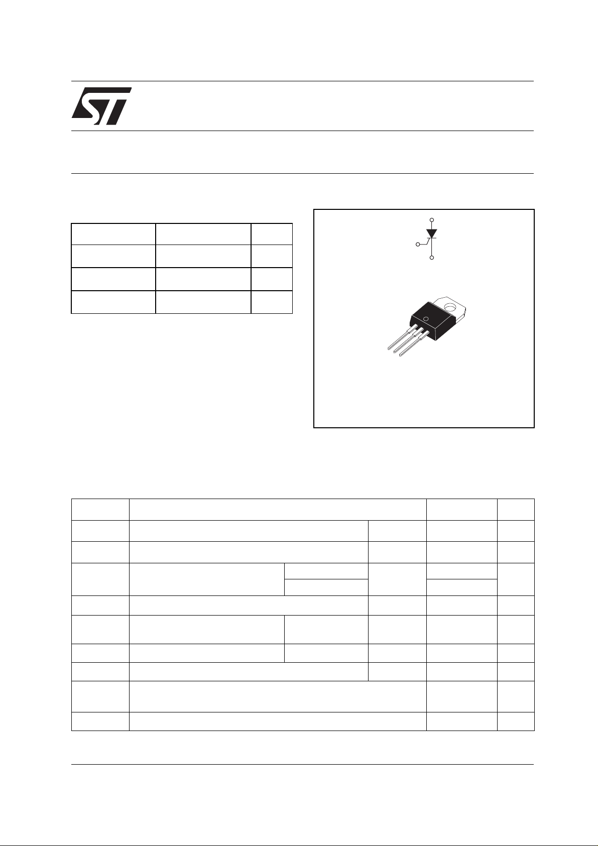
K
A
A
G
K
A
G
TO-220AB
(TYNx40)
ABSOLUTE RATINGS (lim iting values)
Symbol Parameter Value Unit
I
T(RMS)
IT
(AV)
I
TSM
²
I
dI/dt
I
GM
P
G(AV)
T
stg
Tj
V
RGM
April 2002 - Ed: 4A
RMS on-state current (180° conduction angle)
Average on-state current (180° conduction angle)
Non repetitive surge peak on-state
current
tI
²
t Value for fusing
Critical rate of rise of on-state current
= 2 x IGT , tr ≤ 100 ns
I
G
tp = 8.3 ms
tp = 10 ms 460
F = 60 Hz Tj = 125°C 50 A/µs
Tc = 95°C 40
Tc = 95°C 25
Tj = 25°C
Tj = 25°C 1060
Peak gate current tp = 20 µs Tj = 125°C 4 A
Average gate power dissipation Tj = 125°C 1 W
Storage junction temperature range
Operating junction temp erature range
- 40 to + 150
- 40 to + 125
Maximum peak reverse gate voltage 5
480
A
A
A
2
S
A
°C
V
1/4
Page 2
TYNx40 Series
ELECTRICAL CHARACTERISTICS (Tj = 25°C, unless otherwise specified)
Symbol Test Conditions Value Unit
I
GT
VD = 12 V RL = 33 Ω
V
GT
V
GD
I
H
I
L
dV/dt
V
TM
V
t0
R
d
I
DRM
I
RRM
VD = V
IT = 500 mA Gate open
IG = 1.2 I
= 67 % V
V
D
ITM = 80 A tp = 380 µs
Threshold voltage Tj = 125°C MAX. 0.85 V
Dynamic resistance Tj = 125°C MAX. 10 mΩ
V
DRM
RL = 3.3 kΩ
DRM
GT
DRM
= V
RRM
Gate open
Tj = 125°C MIN.
Tj = 125°C MIN. 1000 V/µs
Tj = 25°C MAX. 1.6 V
Tj = 25°C MAX. 5 µA
Tj = 125°C 4 mA
THERMAL RESISTANCES
Symbol Parameter Value Unit
R
R
th(j-c)
th(j-a)
Junction to case (DC)
Junction to ambient (DC)
MIN. 3.5
MAX. 35
MAX. 1.3 V
0.2 V
MAX. 75 mA
MAX. 150 mA
0.8
60
mA
°C/W
°C/W
PRODUCT SELECTOR
Part Number
600 V 800 V 1000 V
TYNx40 X X X 35 mA TO-220AB
Voltage
Sensitivity
Package
ORDERING INFORMATION
TYN 6 40 (RG)
STANDARD
SCR
SERIES
VOLTAGE:
6: 600V
CURRENT:40A
8: 800V
10: 1000V
OTHER INFORMATION
Part Number Marking Weight Base Quantity Packing mode
TYNx40 TYNx40 2.3 g 250 Bulk
TYNx40RG TYNx40 2.3 g 50 Tube
PACKING MODE
Blank: Bulk
RG:Tube
Note: x = voltage
2/4
Page 3

TYNx40 Series
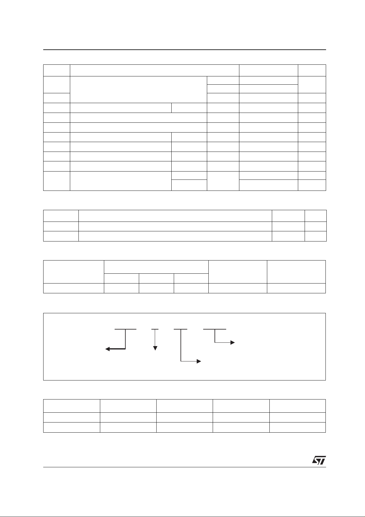
Fig. 1: Maximum average power dissipation
versus average on-state current.
P(W)
40
α = 180°
35
30
25
20
15
10
5
0
0 5 10 15 20 25 30
IT(av)(A)
360°
α
Fig. 3: Relative variation of thermal impeda nce
versus pulse duration.
K = [Zth/Rth]
1.00
Zth(j-c)
0.10
Zth(j-a)
Fig. 2: Average and DC on-state current versus
case temperature.
IT(av)(A)
50
40
30
20
10
0
0 25 50 75 100 125
D.C.
α = 180°
Tcase(°C)
Fig. 4: Relative variation of gate trigger current,
holding current and latching current versus
junction temperature.
IGT,IH,IL [Tj] / IGT,IH,IL [Tj = 25°C]
2.5
2.0
1.5
1.0
IGT
IH & IL
0.01
1E-3 1E-2 1E-1 1E+0 1E+1 1E+2 5E+2
tp(s)
Fig. 5: Surge peak on-state current versus
number of cycles.
ITSM(A)
500
450
400
350
300
250
200
150
100
50
0
1 10 100 1000
Repetitive
Tcase = 95°C
Non repetitive
Tj initial = 25°C
Number of cycles
tp = 10ms
One cycle
0.5
0.0
-40 -20 0 20 40 60 80 100 120 140
Tj(°C)
Fig. 6: Non-repetitive surge peak on-state
current for a sinusoidal pulse with width
tp < 10 ms, and corresponding value of I²t.
ITSM(A),I2t(A2s)
5000
1000
100
0.01 0.10 1.00 10.00
dI/dt
limitattion
tp(ms)
Tj initial = 25°C
ITSM
I2t
3/4
Page 4

TYNx40 Series
Fig. 7: On-state characteristics (maximum
values).
ITM(A)
500
Tj max.:
Vto = 0.85V
Rd = 10mΩ
100
Tj = Tj max.
10
1
0.0 0.5 1.0 1.5 2.0 2.5 3.0 3.5 4.0 4.5 5.0
Tj = 25°C
VTM(V)
PACKAGE MECHANICAL DAT A
TO-220AB (Plastic)
B
L
I
A
l4
a1
l3
l2
a2
b1
e
C
b2
c2
M
c1
DIMENSION S
REF.
Millimeters Inches
Min. Typ. Max. Min. Typ. Max.
A 15.20 15.90 0.598 0.625
F
a1 3.75 0.147
a2 1 3.00 14.00 0.511 0.551
B 10.00 10.40 0.393 0.409
b1 0.61 0.88 0.024 0.034
b2 1.23 1.32 0.048 0.051
C 4.40 4.60 0.173 0.181
c1 0.49 0.70 0.019 0.027
c2 2.40 2.72 0.094 0.107
e 2.40 2.70 0.094 0.106
F 6.20 6.60 0.244 0.259
I 3.75 3.85 0.147 0.151
I4 15.80 16.40 16.80 0.622 0.646 0.661
L 2.65 2.95 0.104 0.116
l2 1.14 1.70 0.044 0.066
l3 1.14 1.70 0.044 0.066
M 2.60 0.102
Information furnishe d is b el i eved to be accura te and reliable. However, STMicroelectroni cs assumes no res ponsibility for the c o nsequences
of use of such information nor for any infringement of patents or other rights of third parties which may result from its use. No license is granted
by implic ation or ot herwise unde r any patent or patent ri ghts of STMi croelectronics. Spec i fications m ent i oned in this publication are subjec t
to change without notice. This publication supersedes and replaces all information previously supplied. STMicroelectronics products are not
authoriz ed for use as crit i cal compone nt s in life supp ort devices or systems witho ut express wr itten approv al of STM i croelect ronics.
© The ST logo is a registe red trademark of STMicroel ectronics
© 2002 STMi croelectroni cs - Printed in It aly - All Rights Reserved
STMicroele ctronics GROUP OF COMPANIES
Australi a - Brazil - Canada - China - Fi nl and - France - Germany
Hong Kong - India - Isreal - Italy - Japan - M a l aysia - Malta - M orocco - Sin gapore
Spain - Sweden - Switzerland - United Ki ngdom - United S t ates.
http:// ww w.st.com
4/4
 Loading...