

Page 1
TLE 4267
5-V Low-Drop Voltage Regulator
Features
● Output voltage tolerance ≤ ± 2 %
● Low-drop voltage
● Very low standby current consumption
● Input voltage up to 40 V
● Overvoltage protection up to 60 V (≤ 400 ms)
● Reset function down to 1 V output voltage
● ESD protection up to 2000 V
● Adjustable reset time
● On/off logic
● Overtemperature protection
● Reverse polarity protection
● Short-circuit proof
● Wide temperature range
● Suitable for use in automotive electronics
TLE 4267
Bipolar IC
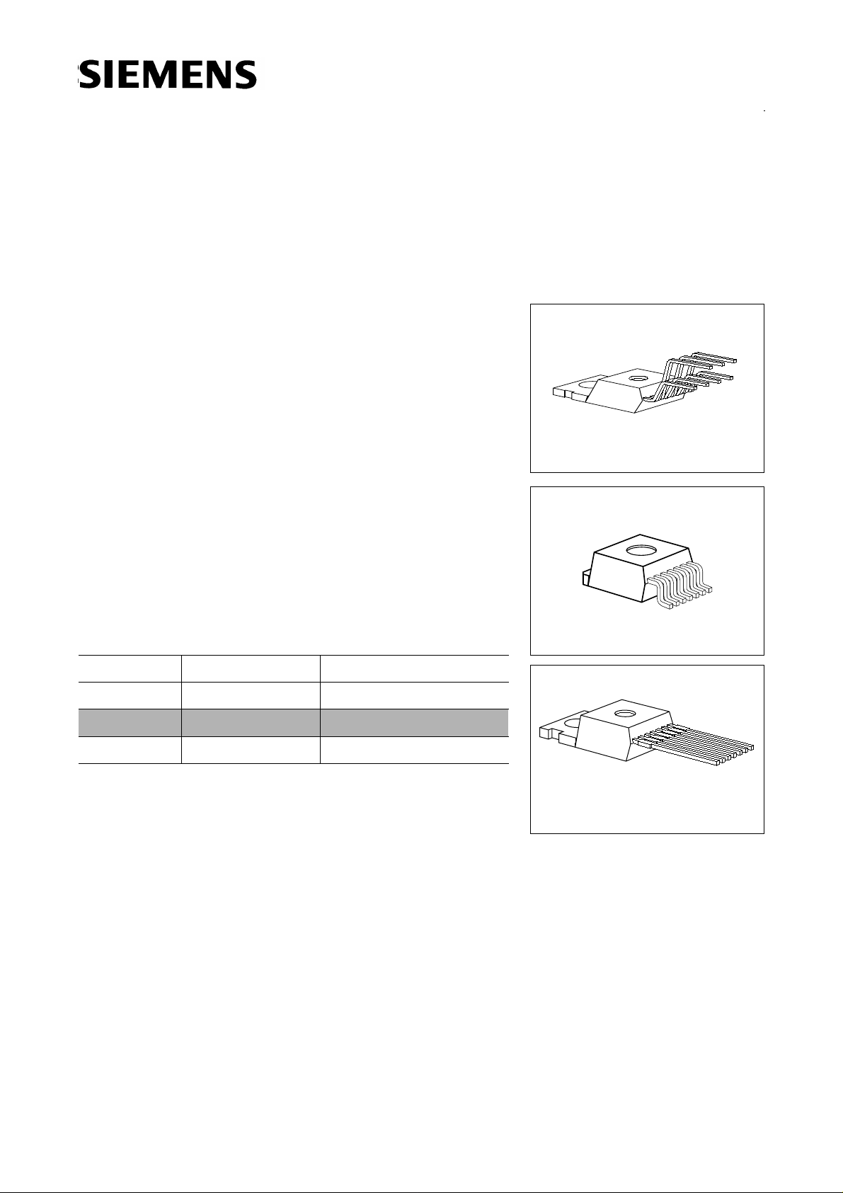
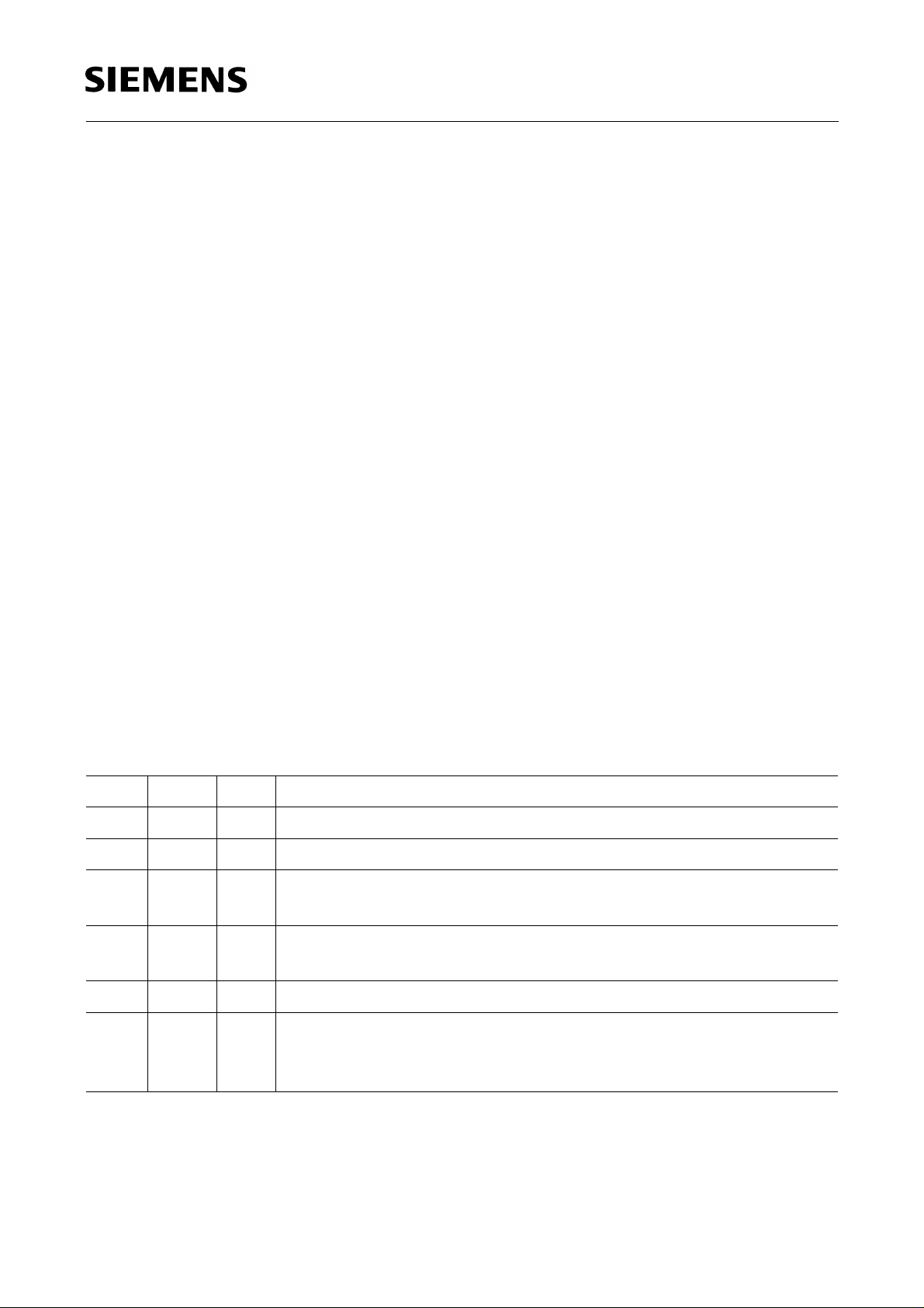
P-TO220-7-3
P-TO220-7-180
Type Ordering Code Package
TLE 4267 Q67000-A9153 P-TO220-7-3
TLE 4267 G Q67006-A9169 P-TO220-7-180 (SMD)
TLE 4267 S Q67000-A9246 P-TO220-7-230
Functional Description
P-TO220-7-230
TLE 4267 is a 5-V low-drop voltage regulator in a
TO220-7 package. It supplies an output current of > 400 mA. The IC is shortcircuit-proof
and incorporates temperature protection that disables the IC at overtemperature.
Application
V
The IC regulates an inp ut voltage
in the range 5.5 V < VI<40V to V
I
reset signal is generated for an output voltage
V
of < 4.5 V. The reset delay can be set
Q
Qrated
=5.0V.A
with an external capacitor. The device has two logic inputs. It is turned-ON by a voltage
of > 4 V on E2 by th e ign itio n for ex amp le. It rem ain s ac tiv e as a func tion of the voltage
on E6, even if the voltage on E2 goes Low. This m akes it pos sible to impl ement a selfholding circuit without external components. When the device is turned-OFF, the output
voltage drops to 0 V and current consumption tends towards 0 µA.
Semiconductor Group 1 1998-11-01
Page 2
TLE 4267
Design Notes for External Components
C
The input capacitor
circuit consisting of lead inductance and input capacitance can be damped by a resistor
of approx. 1 Ω in series with
regulating circuit. Stability is guaranteed at values of ≥ 22 µF and an ESR of ≤ 3 Ω within
the operating temperature range.
Circuit Description
The control amplifier compares a reference voltage, which is kept highly accurate by
resistance adjustmen t, to a voltage that is proportiona l to the output volt age and drives
the base of the series transistor via a buffer. Saturation control as a function of the load
current prevents any over-saturating of the power element.
A comparator in the reset-gen erator bloc k compa res a re ference t hat is ind epende nt of
the input voltage to the scaled-down output voltage. If this reaches a value of 4.5 V, the
reset-delay capacitor is discharged and then the reset output is set Lo w. As the output
voltage increases again, the reset-delay capacitor is charged with constant current from
V
= 4.5 V onwards. When the capacitor voltage reaches the upper switching threshold,
Q
reset goes High again. The reset delay can be set within wide range by selection of the
external capacitor.
is necessary for compensation line influences. The resonant
I
C
. The output capacitor is necessary for the stability of the
I
With the integrated turn-ON/turn-OFF logic it is simple to imp lement delayed turn-OFF
without external components.
Truth Table for Turn-ON/Turn-OFF Logic
Pin 2 Pin 6
V
Q
Remarks
L X OFF Initial state, pin 6 internally pulled up
H X ON Regulator switched on via pin 2, by ignition for example
H L ON Pin 6 clamped active to ground by controller while pin 2 is still
high
X L ON Previous state remains, even ignition is shut off: self-holding
state
L L ON Ignition shut off while regulator is in self-holding state
L H OFF Regulator shut down by releasing of pin 6 while pin 2 remains
Low, final state. No active clamping required by external self-
holding circuit (µC) to keep regulator shut off.
Pin 2: (Inhibit, E2) Enable function, active High
Pin 6: (Hold, E6) H old and relea se func tio n, activ e Low
Semiconductor Group 2 1998-11-01
Page 3
Pin Configuration
(top view)
TLE 4267
P-TO220-7-3 P-TO220-7-230
43215
6
7
Ι
R
E2
GND
D
E6
AEP01481
Q
P-TO220-7-180
Ι
E2
R
D
GND
7651234
E6
AEP01724
4321567
Ι
R
D
E2
GND
E6
Q
AEP02123
Pin Definitions and Functions
Pin Symbol Function
1
I Input; block to ground directly at the IC by a ceramic capacitor
2E2Inhibit; device is turned-ON by High signal on this pin; internal
pulldown resistor of 100 kΩ
3RReset Output; open-collector output internally connected to
the output via a resistor of 30 kΩ
4GNDGround; connected to rear of chip
5DReset Delay; connect with capacitor to GND for setting delay
6E6Hold; see truth table above for function; this input is connected
to output voltage across pullup resistor of 50 kΩ
7Q5-V Output; block to GND with 22-µF capacitor, ESR < 3 Ω
Semiconductor Group 3 1998-11-01
Page 4
TLE 4267
1
In-
put
Adjustment
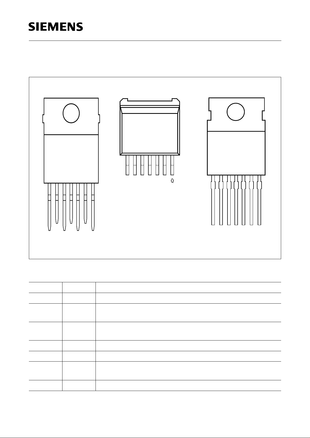
Block Diagram
Temperature
Sensor
Bandgap
Reference
Turn-ON/Turn-OFF
Amplifier
Logic
2
Control
E6 HoldInhibit
6
Buffer
Saturation
Control and
Protection Circuit
4
GND
Reset
Generator
7
5V
Output
5
Reset
Delay
3
Reset
Output
AEB01482
Absolute Maximum Ratings
T
= – 40 to 150 °C
J
Parameter Symbol Limit Values Unit Notes
min. max.
Input
Voltage
Voltage
Current
V
V
I
I
I
I
– 42 42 V –
–60Vt ≤ 400 ms
– – – Limited internally
Reset Output
Voltage
Current
V
I
R
R
– 0.3 7 V –
– – – Limited internally
Reset Delay
Voltage
V
d
– 0.3 42 V –
Semiconductor Group 4 1998-11-01
Page 5
Absolute Maximum Ratings (cont’d)
T
= – 40 to 150 °C
J
Parameter Symbol Limit Values Unit Notes
min. max.
TLE 4267
Current
Output
Voltage
Current
Inhibit
Voltage
Current
Hold
Voltage
Current
GND
Current
I
d
V
I
Q
V
I
E2
V
I
E6
I
GND
Q
E2
E6
––––
– 0.3 7 V –
– – – Limited internally
– 42 42 V
– 5 5 mA t ≤ 400 ms
– 0.3 7 V –
– – mA Limited internally
– 0.5 – A –
Temperatures
Junction temperature
Storage temperature
T
J
T
stg
–150°C–
– 50 150 °C–
Operating Range
Parameter Symbol Limit Values Unit Notes
min. max.
Input voltage
Junction temperature
V
T
I
J
5.5 40 V see diagram
– 40 150 °C–
Thermal Resistance
Junction ambient
Junction-case
Junction-case
R
R
R
thja
thjc
thjc
–70K/W–
–6K/W–
–2K/Wt < 1 ms
Semiconductor Group 5 1998-11-01
Page 6

TLE 4267
Characteristics
V
= 13.5 V; – 40 °C < TJ < 125 °C; VE2 > 4 V (unless specified otherwise)
I
Parameter Symbol Limit Values Unit Test Condition
min. typ. max.
Output voltage
Output voltage
Output-current limiting
Current consumption
I
= II – I
q
Q
Current consumption
I
= II – I
q
Q
Current consumption
I
= II – I
q
Q
Current consumption
I
= II – I
q
Q
Current consumption
I
= II – I
q
Q
Drop voltage
V
V
I
I
I
I
I
I
V
Q
Q
Q
q
q
4.9 5 5.1 V 5 mA ≤ IQ ≤ 400 mA
V
6 V ≤
≤ 26 V
I
4.9 5 5.1 V 5 mA ≤ IQ ≤ 150 mA
V
6 V ≤
≤ 40 V
I
500 – – mA TJ = 25 °C
––50µA Regulator-OFF
–1.010µA TJ = 25 °C
IC turned off
q
–1.34mAIQ = 5 mA
IC turned on
q
q
Dr
––60mAIQ = 400 mA
––80mAIQ = 400 mA
V
= 5 V
I
–0.30.6VIQ = 400 mA
1)
Load regulation ∆V
Supply-voltage
Q
V
∆
Q
regulation
Supply-voltage rejection
Longterm stability
1) Drop voltage = VI – VQ (measured when the output voltage VQ has dropped 100 mV from the
nominal value obtained at
SVR
∆V
Q
V
= 13.5 V)
I
––50mV5 mA ≤ IQ ≤ 400 mA
– 1525mVVI = 6 to 36 V; IQ = 5
mA
–54–dBfr = 100 Hz; Vr = 0.5
V
pp
–0–mV1000 h
Semiconductor Group 6 1998-11-01
Page 7

TLE 4267
Characteristics (cont’d)
Parameter Symbol Limit Values Unit Test Condition
min. typ. max.
Reset Generator
Switching threshold
V
rt
4.2 4.5 4.8 V –
Reset High level – 4.5 – – V
Saturation voltage
V
Pullup R
Saturation voltage
V
Charge curre nt I
Delay switching threshold
Delay
Switching threshold
Delay
V
t
V
t
R
R
D,sat
d
dt
d
st
t
–0.10.4VRR = 4.7 kΩ
–30–kΩ –
– 50 100 mV VQ < V
81525µA VD = 1.5 V
2.6 3 3.3 V –
–20–msCd = 100 nF
–0.43–V–
–2–µs Cd = 100 nF
Inhibit
Turn-ON voltage
Turn-OFF voltage
Pulldown
V
V
R
E2
E2
E2
–34VIC turned-ON
2––VIC turned-OFF
50 100 200 kΩ –
R
ext
= ∞
1)
RT
Hysteresis ∆
Input current
Holding voltage
I
V
Turn-OFF voltage V
Pullup R
E2
V
E6
E6
E6
E2
0.2 0.5 0.8 V –
– 35 100 µA V
30 35 40 % Referred to V
60 70 80 % Referred to V
20 50 100 kΩ –
Overvoltage Protection
Turn-OFF voltage
Turn-ON hysteresis ∆
1) The reset output is Low between VQ = 1 V and V
V
i,ov
V
i,ov
42 44 46 V –
2–6V–
RT
= 4 V
IP2
Q
Q
Semiconductor Group 7 1998-11-01
Page 8

TLE 4267
V
Ι
Test Circuit
Ι
Ι
1000 F 470 nF
µµ
Ι
V
E2
E2
1
TLE 4267
2
5
Ι
d
V
C
C
D
4
Ι
GND
6
V
E6
Ι
Q
7
22 F
Ι
R
3
Ω4.7 k
V
V
R
AES01483
Q
Input
1
7
5 V Output
470 nF
E2; eg
from Terminal 15
Reset
To MC
2
4267TLE
5
22 Fµ
3
100 nF
4
6
E6 From Cµ
AES01484
Application Circuit
Semiconductor Group 8 1998-11-01
Page 9

TLE 4267
V
i
V
E
V
ON
E2,
V
OFFE2,
V
V
RT
V
dT
V
ST
d, sat
satVR,
t
<
V
Q
t
V
d
V
R
t
d
Power
Thermal Voltage Drop
Reset Shutdown
at Input
t
Undervoltage
at Output
t
Secondary
Load Shutdownon
Spike Bounce
AET01985
Time Response
Semiconductor Group 9 1998-11-01
Page 10

TLE 4267
V
i
V
E2
V
E2, OFF
V
V
E6,
V
Q,
V
E2,VON
E6,
rel
hold
V
RT
V
dT
V
ST
sat
d,
1)
V
E6
2) 4)
V
Q
5)
µµ
s
6)
10 s<<1
10)
8)
V
d
V
R
t
d
t
t
µ
Cµ
for more
9)
AET01986
V
R,
sat
1) Enable active
Hold inactive, pulled up by 2)
3) Power-ON reset
4) Hold active, clamped to
3)
GND by external µ
C
5) Enable inactive, clamped by int.
pull-down resistor
6) Pulse width smaller than 1 s
V
Q
7) Hold inactive, released by
8) Voltage controller shutdown
9) Output-low reset
10) No switch on via
was released to
s
µ
than 4
V
possible after E6
E6
V
>
V
E6
E6, rel
Enable and Hold Behaviour
Semiconductor Group 10 1998-11-01
Page 11

TLE 4267
Output Voltage VQ versus
T
Temperature
5.10
V
Q
V
5.00
4.90
4.80
4.70
-40
j
V
=
13.5 V
Ι
0 40 80 160
AED01486
C
T
j
Drop Voltage
V
Output Current
700
V
Dr
mV
500
400
T
=
j
300
200
100
0
0
200 300 400
100
versus
Dr
I
Q
125
C
T
=25
j
AED01488
C
mA
Ι
600
Q
Charge Current
Temperature
22
Ι
d
A
µ
18
16
14
12
10
-40
T
j
0 40 80 160
I
versus
d
V
=13.5 V
Ι
V
=0 V
C
Ι
d
AED01485
C
T
j
Delay Switching Threshold
T
Temperature
4.0
V
dT
V
3.0
2.5
2.0
1.5
1.0
0.5
0
-40
j
V
= 13.5 V
Ι
V
dT
0 40 80 160
V
versus
dT
AED01487
C
T
j
Semiconductor Group 11 1998-11-01
Page 12

TLE 4267
Current Consumption Iq versus
I
Output Current
70
Ι
q
mA
50
40
30
20
10
0
100
0
Q
V
= 13.5 V
Ι
200 300 400
AED01490
mA
Ι
Current Consumption
V
Input Voltage
15
Ι
q
I
R
L
I
versus
q
AED01491
Ω25
=
mA
10
5
0
10
600
Q
0
20 30 50
V
V
Ι
Output Current
Temperature
700
Ι
Q
mA
500
400
300
200
100
0
-40
T
0 40 80 160
I
versus
Q
j
V
Ι
I
Q
V
I
T
=
j
versus
AED01987
C25
AED01489
Output Current
Input Voltage
700
mA
Ι
Q
600
500
13.5 V=
T
125 C=
j
400
300
200
100
0
C
T
j
10 20 30 40 50
0
V
V
i
Semiconductor Group 12 1998-11-01
Page 13

TLE 4267
Output Voltage VQ versus
V
Inhibit Voltage
6
V
V
Q
5
4
3
2
1
0
0
1 2
E2
3
AED01988
Inhibit Current
Inhibit Voltage
50
Aµ
Ι
E2
I
versus
E2
V
E2
AED01989
40
30
20
10
5
4
6
V
V
E2
0
0
1 2
3
5
4
6
V
V
E2
Semiconductor Group 13 1998-11-01
Page 14

Package Outlines
P-TO220-7-3
(Plastic Transistor Single Outline)
TLE 4267
Sorts of Packing
Package outlines for tubes, trays etc. are contained in our
Data Book “Package Information”
Dimensions in mm
Semiconductor Group 14 1998-11-01
Page 15

P-TO220-7-180
(Plastic Transistor Single Outline)
TLE 4267
Sorts of Packing
Package outlines for tubes, trays etc. are contained in our
Data Book “Package Information”
SMD = Surface Mounted Device
Dimensions in mm
Semiconductor Group 15 1998-11-01
Page 16

P-TO220-7-230
(Plastic Transistor Single Outline)
TLE 4267
Sorts of Packing
Package outlines for tubes, trays etc. are contained in our
Data Book “Package Information”
Dimensions in mm
Semiconductor Group 16 1998-11-01
 Loading...