

Page 1
TLE 4266
5-V Low-Drop Voltage Regulator
Features
● Output voltage tolerance ≤ ± 2%
● Very low current consumption
● Low-drop voltage
● Overtemperature protection
● Reverse polarity proof
● Wide temperature range
● Suitable for use in automotive electronics
● Inhibit
Type Ordering Code Package
P-SOT223-4-2
TLE 4266
Bipolar IC
TLE 4266 G Q67006-A9152 P-SOT223-4-2 (SMD)
TLE 4266 GSV10 Q67006-A9355 P-SOT223-4-2 (SMD)
▼
▼ New type
Functional Description
TLE 4266 G is a 5-V low-drop voltage regulator in a P-SOT2 23-4-2 SMD pa ck age . The
IC regulates an input voltage
in the range of 5.5 V < Vi < 45 V to V
i
= 5 V / 10 V.
Qrated
V
The maximum output current is m ore than 120 mA. The IC can be switched off via the
inhibit input, which causes the current consumption to drop below 10 µA. The IC is
shortcircuit-proof and incorporates temperature protection that disables the IC an
overtemperature.
Dimensioning Information on External Components
C
The input capacitor
approx. 1 Ω in series with
be clamped. The output capacitor
circuit. Stability is guaranteed at values
is necessary for compensating line influences. Using a resistor of
i
C
, the oscillating of input inductivity and input capacitance can
i
C
is necessary for the stability of the regulating
Q
C
≥ 10 µF and an ESR ≤ 10 Ω within the
Q
operating temperature range.
Semiconductor Group 1 1998-11-01
Page 2
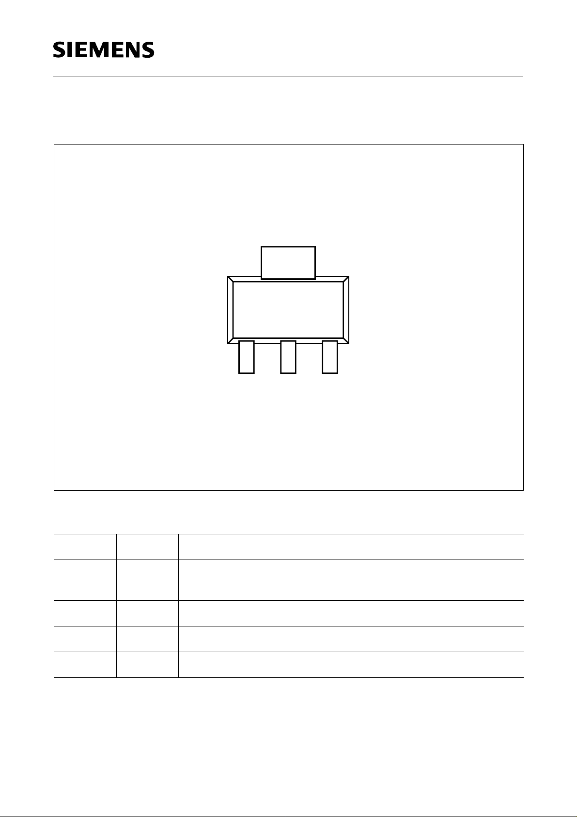
Pin Configuration
(top view)
TLE 4266
GND
4
Pin Definitions and Functions
Pin Symbol Function
1
V
I
Input voltage; block to ground directly at the IC with a ceramic
capacitor.
123
V
Ι
Inh
V
Q
AEP01734
2InhInhibit; low-active input.
3
V
Q
Output voltage; block to ground with a ≥ 10 µF capacitor.
4GNDGround
Semiconductor Group 2 1998-11-01
Page 3
TLE 4266
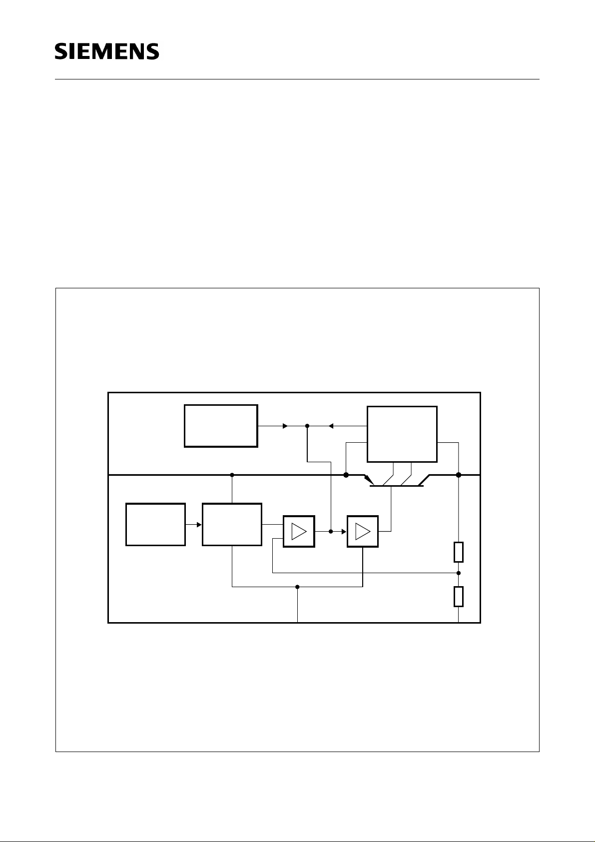
Circuit Description
The control amplifier compares a reference voltage, which is kept highly accurate by
resistance adjustmen t, to a voltage that is proportiona l to the output volt age and drives
the base of the series transistor via a buffer. Saturation control as a function of the load
current prevents any oversaturation of the power element. The IC also incorporates a
number of internal circuits for protection against:
● Overload
● Overtemperature
● Reverse polarity
1
Adjustment
Temperature
Sensor
Bandgap
Reference
Saturation
Control and
Protection
Circuit
Control
Amplifier Buffer
Inhibit GND
AEB01725
3
OutputInput
42
Block Diagram
Semiconductor Group 3 1998-11-01
Page 4

Absolute Maximum Ratings
T
= – 40 to 150 °C
j
Parameter Symbol Limit Values Unit Notes
min. max.
Input
TLE 4266
Voltage
Current
Inhibit
Voltage
Output
Voltage
Current
GND
Current
Temperature
Junction temperature
V
I
V
V
I
I
T
i
i
e
Q
Q
M
j
– 42 45 V –
– – – internally limited
– 42 45 V –
– 1 16 V –
– – – internally limited
50 – mA –
– 150 °C–
Storage temperature
T
S
– 50 150 °C–
Operating Range
Input voltage
Input voltage
V
V
i
i
5.5 45 V –
10.5 45 V –
GSV 10-version
Junction temperature
T
j
– 40 150 °C–
Thermal Resistance
Junction ambient
Junction case
Semiconductor Group 4 1998-11-01
R
R
thjA
thjC
– 100 K/W soldered
–25K/W–
Page 5

TLE 4266
Characteristics
V
= 13.5 V; – 40 °C ≤ Tj ≤ 125 °C
I
Parameter Symbol Limit Values Unit Test Condition
min. typ. max.
Output voltage
Output voltage
V
V
GSV 10-version
Output-current
I
Q
limitation
Current consumption
I
= Ii – I
q
Q
Current consumption
I
= Ii – I
q
Q
Current consumption
I
= Ii – I
q
Q
Drop voltage
I
I
I
V
q
q
q
Load regulation ∆V
Q
Q
4.95 5.1V5 mA ≤ IQ ≤ 100 mA
V
6 V ≤
≤ 28 V
i
9.8 10.0 10.2 V 5 mA ≤ IQ ≤ 100 mA
V
6 V ≤
≤ 28 V
i
120 150 – mA –
–010µA Ve = 0 V; Tj ≤ 100 °C
––400µA IQ = 1 mA
– 1015mAIQ = 100 mA
Dr
Q
– 0.25 0.5 V IQ = 100 mA
––40mVIQ = 5 to 100 mA
V
= 6 V
i
1)
Supply-voltage
regulation
Supply-voltage
rejection
V
∆
SVR
Q
– 1530mVVI = 6 V to 28 V
I
= 5 mA
Q
–54–dBfr = 100 Hz
V
= 0.5 V
r
SS
Inhibit
Inhibit on voltage
Inhibit off voltage
Inhibit cu rrent
1) Drop voltage = Vi – VQ (measured when the output voltage VQ has dropped 100 mV from the
nominal value obtained at
Semiconductor Group 5 1998-11-01
V
e, on
V
e, off
I
e
V
= 13.5 V).
i
––3.5V–
0.8 – – V –
51525µA Ve = 5 V
Page 6

Input
5.5 V to 45 V
TLE 4266
1
3
Output
V
i
Measuring Circuit
Ι
i
470 µF
V
e
Ι
Q
nF100
TLE 4266G
µF22
V
Q
2
Ι
e
4
AES01726
Input
C
Q
Output
µF22
5.5 V to 45 V
1
C
i
TLE 4266G
3
2
e.g. Kl. 15
4
AES01727
Application Circuit
Semiconductor Group 6 1998-11-01
Page 7

TLE 4266
Drop Voltage VDr versus
I
Output Current
800
mV
V
Dr
700
600
500
400
300
200
100
0
25
50 100
Q
75
T
=
j
25 C=
T
j
C125
125
mA
Current Consumption
V
Input Voltage
15
mA
Ι
q
i
I
versus
q
AED01979
10
R
=
50 Ω
L
5
Ω100
=
R
L
175
Ι
Q
0
0
10 20 30
40
50
V
V
i
Current Consumption
I
Output Current
12
Ι
mA
q
10
8
6
4
2
0
0
Q
V
= 13.5 V
i
I
versus
q
AED01980
mA
Ι
Q
I
Current Consumption
I
Output Current
3.0
Ι
mA
q
Q
versus
q
AED01981
2.5
2.0
1.5
1.0
V
= 13.5 V
i
0.5
0
5
15050 100
0
15
mA
3010 20
Ι
Q
Semiconductor Group 7 1998-11-01
Page 8

TLE 4266
Output Voltage VQ versus
T
Temperature
5.20
V
V
Q
5.10
5.00
4.90
4.80
4.70
4.60
-40
(5 V-version)
j
V
= 13.5 V
i
04080 160
AED01982
120
T
Output Current
Input Voltage
200
mA
Ι
Q
V
I
i
versus
Q
AED01983
150
25 C
=
T
j
100
= C125
T
j
50
0
C
j
10 20 30 40 50
0
V
V
i
Output Voltage
Input Voltage
6
V
V
Q
5
4
3
2
1
0
0
V
24
V
versus
Q
(5 V-version)
i
R
L
6
AED01984
=50Ω
8
V
V
Output Voltage
Inhibit Voltage
6
V
V
Q
versus
Q
V
(5 V-version)
e
AED02014
5
V
= 13.5 V
Ι
4
=
V
V
Ι e
3
2
1
10
V
i
0
0
1234
5
6
V
V
e
Semiconductor Group 8 1998-11-01
Page 9

Package Outlines
P-SOT223-4-2
(Plastic Small Outline Transistor)
±0.2
A
6.5
3
±0.1
0.1 max
1.6
TLE 4266
±0.1
Weight approx. 0.15 g
B
0.7
±0.1
0.25
4
+0.2
acc. to
DIN 6784
21
3
2.3
±0.3
7
15˚max
min
0.5
0.28
±0.2
3.5
±0.04
4.6
M
A
0.25
M
B
GPS05560
Sorts of Packing
Package outlines for tubes, trays etc. are contained in our
Data Book “Package Information”
SMD = Surface Mounted Device
Dimensions in mm
Semiconductor Group 9 1998-11-01
 Loading...