

Page 1
TLE 4266
5-V Low-Drop Voltage Regulator
Features
● Output voltage tolerance ≤± 2%
● Very low current consumption
● Low-drop voltage
● Overtemperature protection
● Reverse polarity proof
● Wide temperature range
● Suitable for use in automotive electronics
● Inhibit
Type Ordering Code Package
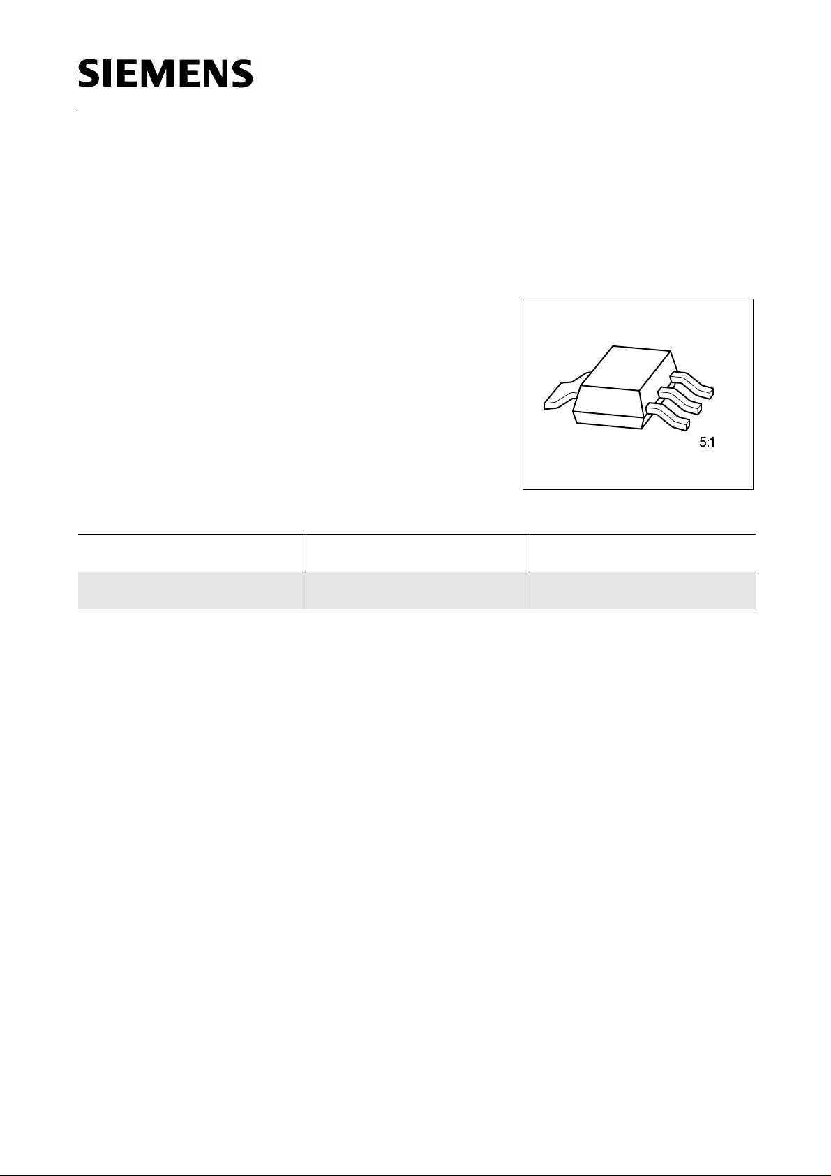
P-SOT223-4-2
TLE 4266
Bipolar IC
TLE 4266 G Q67006-A9152 P-SOT223-4-2
▼
▼ New type
Functional Description
TLE 4266 G is a 5 V low-drop voltage regulator in a P-SOT223-4-2 SMD package. The
IC regulates an input voltage
in the range of 5.5 V < Vi < 45 V to V
i
= 5 V. The
Qrated
V
maximum output current is more than 120 mA. The IC can be switched off via the inhibit
input, which causes the current consumption to drop below 10 µA. The IC is shortcircuitproof and incorporates temperature protection that disables the IC an overtemperature.
Dimensioning Information on External Components
C
The input capacitor
approx. 1 Ω in series with
be clamped. The output capacitor
circuit. Stability is guaranteed at values
is necessary for compensating line influences. Using a resistor of
i
C
, the oscillating of input inductivity and input capacitance can
i
C
is necessary for the stability of the regulating
Q
C
≥ 10 µF and an ESR ≤ 10 Ω within the
Q
operating temperature range.
Semiconductor Group 1
11.96
Page 2
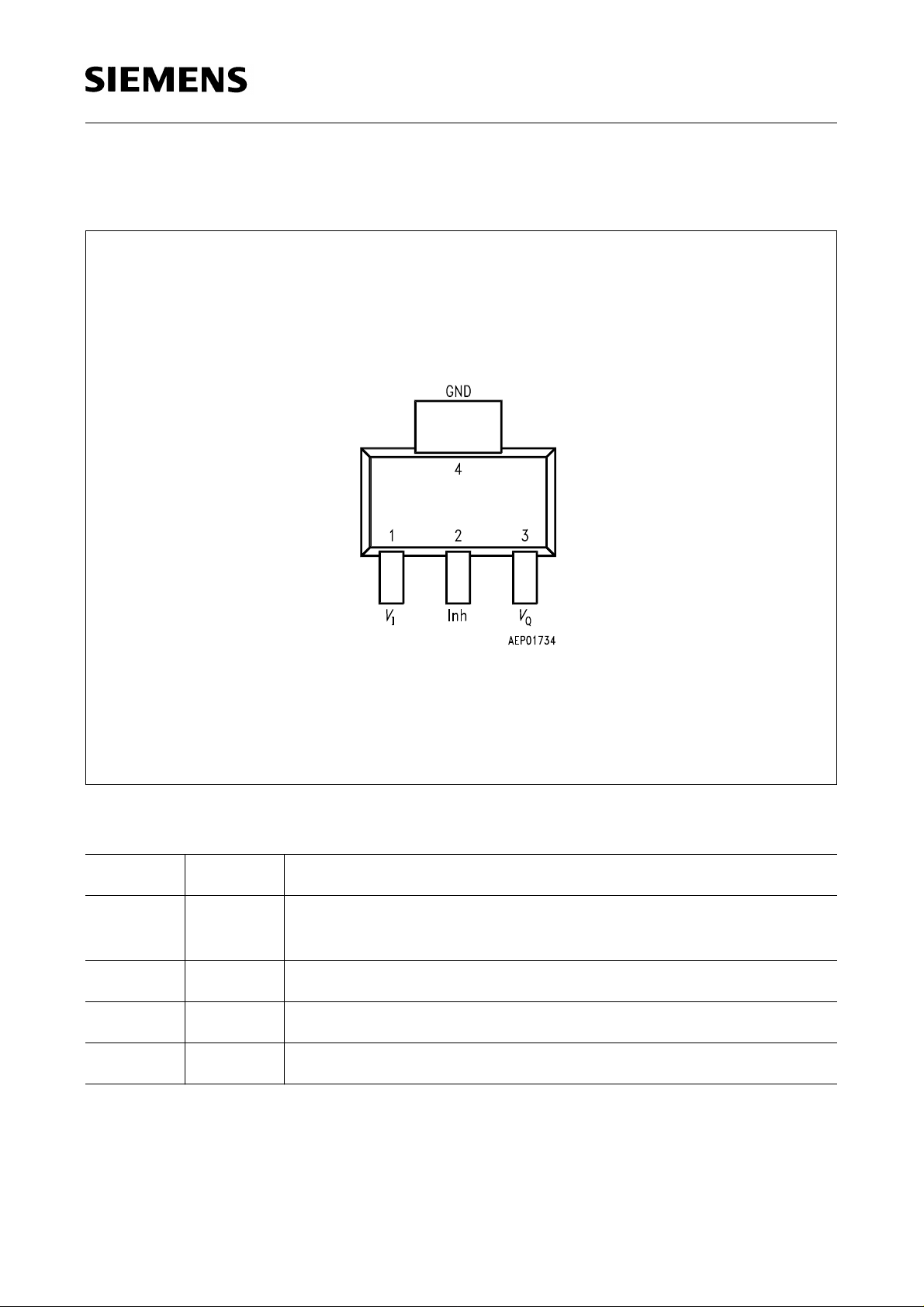
Pin Configuration
(top view)
TLE 4266
Pin Definitions and Functions
Pin Symbol Function
1
V
I
Input voltage; block to ground directly at the IC with a ceramic
capacitor.
2 Inh Inhibit; low-active input.
3
V
Q
5-V output voltage; block to ground with a ≥ 10 µF capacitor.
4 GND Ground
Semiconductor Group 2
Page 3
TLE 4266
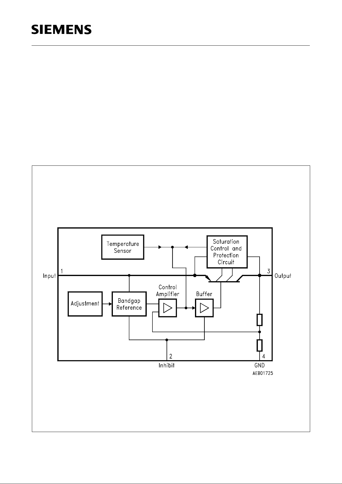
Circuit Description
The control amplifier compares a reference voltage, which is kept highly accurate by
resistance adjustment, to a voltage that is proportional to the output voltage and drives
the base of the series transistor via a buffer. Saturation control as a function of the load
current prevents any oversaturation of the power element. The IC also incorporates a
number of internal circuits for protection against:
● Overload,
● Overtemperature,
● Reverse polarity.
Block Diagram
Semiconductor Group 3
Page 4

Absolute Maximum Ratings
T
= – 40 to 150 °C
j
Parameter Symbol Limit Values Unit Notes
min. max.
Input
TLE 4266
Voltage
Current
Inhibit
Voltage
Output
Voltage
Current
GND
Current
Temperature
Junction temperature
V
I
V
V
I
I
T
i
i
e
Q
Q
M
j
– 42 45 V
internally limited
– 42 45 V
– 1 16 V
internally limited
50 mA
150 °C
Storage temperature
T
S
– 50 150 °C
Operating Range
Input voltage V
Junction temperature
T
i
j
5.5 45 V
– 40 150 °C
Thermal Resistance
Junction ambient
Junction case
R
R
thjA
thjC
Semiconductor Group 4
100 K/W soldered
25 K/W
Page 5

TLE 4266
Characteristics
V
= 13.5 V; – 40 °C ≤ Tj≤ 125 °C
I
Parameter Symbol Limit Values Unit Test Condition
min. typ. max.
Output voltage
Output-current
V
I
Q
limitation
Current consumption
I
= Ii – I
q
Q
Current consumption
I
= Ii – I
q
Q
Current consumption
I
= Ii – I
q
Q
Drop voltage
I
I
I
V
q
q
q
Load regulation ∆V
Supply-voltage
∆
V
regulation
Q
Dr
4.9 5 5.1 V 5 mA ≤ IQ≤ 100 mA
6 V ≤
V
≤ 28 V
i
120 150 mA
010µAV
= 0 V; Tj≤ 100 °C
e
400 µA IQ = 1 mA
10 15 mA IQ = 100 mA
0.25 0.5 V IQ = 100 mA
Q
Q
15 30 mV VI = 6 V to 28 V
40 mV IQ = 5 to 100 mA
V
= 6 V
i
I
= 5 mA
Q
1)
Supply-voltage
rejection
SVR
54 dB fr = 100 Hz
V
= 0.5 V
r
SS
Inhibit
Inhibit on voltage
Inhibit off voltage
Inhibit current
1) Drop voltage = Vi – VQ (measured when the output voltage VQ has dropped 100 mV from the
nominal value obtained at Vi = 13.5 V).
V
V
I
e, on
e, off
e
3.5 V
0.8 V
51525µAV
= 5 V
e
Semiconductor Group 5
Page 6

TLE 4266
Measuring Circuit
Application Circuit
Semiconductor Group 6
Page 7

Drop Voltage
V
Output Current
versus
Dr
I
Q
TLE 4266
Current Consumption Iq versus
Input Voltage
V
i
Current Consumption Iq versus
Output Current
I
Q
Current Consumption Iq versus
Output Current
I
Q
Semiconductor Group 7
Page 8

Output Voltage
Temperature
T
V
Q
j
versus
Output Current IQ versus
Input Voltage
V
i
TLE 4266
Output Voltage VQ versus
Input Voltage
V
i
Output Voltage VQ versus
Inhibit Voltage
V
e
Semiconductor Group 8
Page 9

Package Outlines
P-SOT223-4-2 (SMD)
(Plastic Small Outline Transistor)
TLE 4266
Weight approx. 0.15 g
Sorts of Packing
Package outlines for tubes, trays etc. are contained in our
Data Book “Package Information”
SMD = Surface Mounted Device
GPS05560
Dimensions in mm
Semiconductor Group 9
 Loading...