

Page 1
TLE 4264 G
5-V Low-Drop Fixed-Voltage Regulator
TLE 4264 G
Features
● Output voltage tolerance ≤ ± 2 %
● Low-drop voltage
● Very low current consumption
● Overtemperature protection
● Short-circuit proof
● Suitable for use in automotive electronics
● Reverse polarity
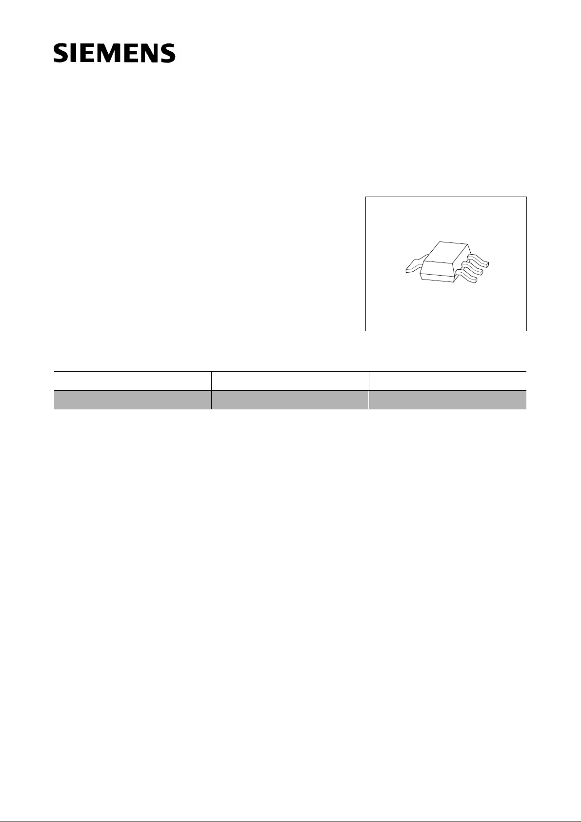
P-SOT223-4-1
Type Ordering Code Package
TLE 4264 G Q67006-A9139 P-SOT223-4-1 (SMD)
Functional Description
TLE 4264 G is a 5-V low-drop fixed-voltage regul ator in an SOT-223 package. The IC
regulates an input voltage
in the range 5.5 V < VI < 45 V to V
I
= 5.0 V. The
Qrated
V
maximum output current is more than 120 mA. This IC is shortcircuit-proof and features
temperature protection that disables the circuit at overtemperature.
Dimensioning Information on External Components
C
The input capacitor
approx. 1 Ω in series with
be clamped. The output capacitor
circuit. Stability is guaranteed at values
is necessary for compensating line influences. Using a resistor of
i
C
, the oscillating of input inductivity and input capacitance can
i
C
is necessary for the stability of the regulating
Q
C
≥ 10 µF and an ESR ≤ 10 Ω within the
Q
operating temperature range.
Semiconductor Group 1 1998-11-01
Page 2
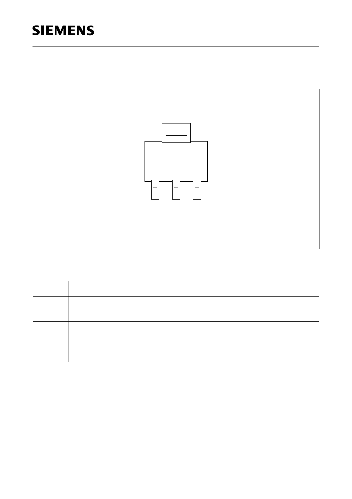
Pin Configuration
(top view)
TLE 4264 G
4
123
V
Pin Definitions and Functions
Pin Symbol Function
1
V
I
Input voltage; block to ground directly on IC with
ceramic capacitor
2, 4 GND Ground
3
V
Q
5-V output voltage; block to ground with ≥ 10-µF
capacitor, ESR < 10 Ω
Circuit Description
GND
V
QΙ
AEP01526
The control amplifier compares a reference voltage, which is kept highly precise by
resistance adjustment, to a voltag e t hat is proporti onal to the o utput v oltage and d rives
the base of the series transistor via a buffer. Saturation control, working as a function of
load current, prevents any over-sat uration of the power element . The IC is additionally
protected against overload, overtemperature and reverse polarity.
Semiconductor Group 2 1998-11-01
Page 3
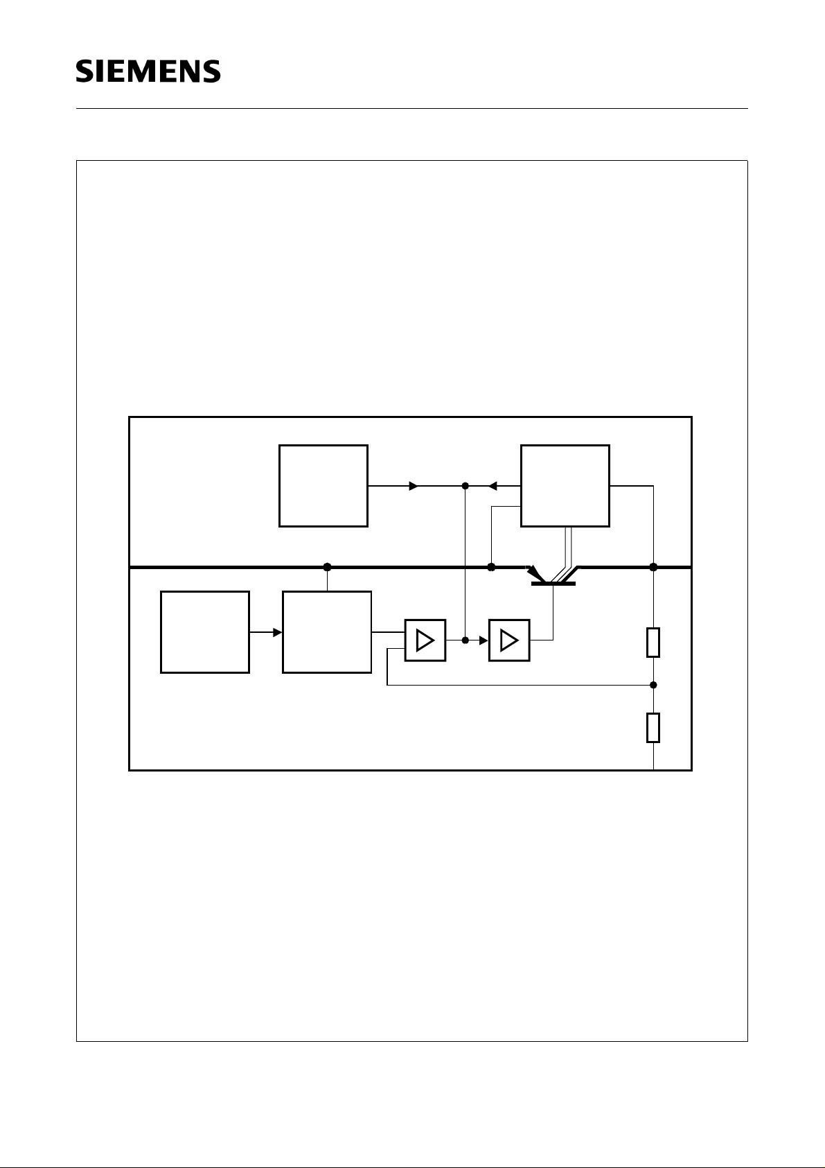
Temperature
Sensor
TLE 4264 G
Saturation
Control and
Protection
Circuit
Input
2,4
GND
AEB01527
3
Output
1
Control
Adjustment
Amplifier
Bandgap
Reference
Buffer
Block Diagram
Semiconductor Group 3 1998-11-01
Page 4

TLE 4264 G
Absolute Maximum Ratings
T
= – 40 to 150 °C
j
Parameter Symbol Limit Values Unit Notes
min. max.
Input
Input voltage
Input current
Output
Output voltage
Output current
Ground
Current
Temperatures
Junction temperature
Storage temperature
V
I
V
I
I
T
T
I
I
Q
Q
GND
j
stg
–42 45 V –
– – – limited internally
–1 16 V –
– – – limited internally
50 – mA –
–150°C–
–50 150 °C–
Operating Range
V
Input voltage
Junction temperature
5.5 45 V –
I
T
j
–40 150 °C–
Thermal Resistances
System-air
System-case
Semiconductor Group 4 1998-11-01
R
R
th SA
th SC
– 100 K/W soldered in
–25K/W–
Page 5

TLE 4264 G
Characteristics
V
= 13.5 V; – 40 °C ≤ Tj ≤ 125 °C, unless specified otherwise
I
Parameter Symbol Limit Values Unit Test Conditions
min. typ. max.
Output voltage
V
Output-current
limiting
I
Q
Current consumption
I
= II – I
q
Q
I
q
Current consumption
I
= II – I
q
Q
Drop voltage
I
V
q
Load regulation ∆V
Supply-voltage
V
∆
regulation
Supply voltage
SVR
suppression
Q
4.9 5.0 5.1 V 5 mA ≤ IQ ≤ 100 mA
V
6V ≤
≤ 28 V
I
120 150 – mA –
– – 400 µA IQ = 1 mA
– 1015mAIQ = 100 mA
dr
Q
Q
– 0.25 0.5 V IQ = 100 mA
––40mVIQ = 5 to 100 mA
V
= 6 V
I
– 1530mVVI = 6 to 28 V
I
= 5 mA
Q
1)
–54–dBfr = 100 Hz
V
= 0.5 Vpp
r
1)
Drop voltage = VI –VQ (measured where VQ has dropped 100 mV from the nominal value
obtained at
Semiconductor Group 5 1998-11-01
V
= 13.5 V)
I
Page 6

TLE 4264 G
Application Circuit
Input
5.5 to 45 V
1
C
i
TLE 4264G
2,4
3
Output
µ10 F
AES01528
Semiconductor Group 6 1998-11-01
Page 7

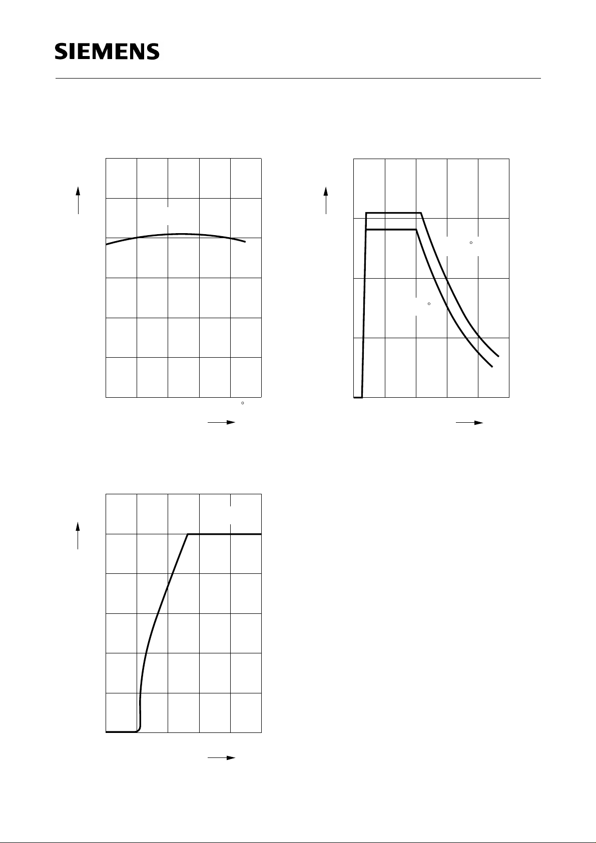
TLE 4264 G
Drop Voltage VDr versus
I
75
Q
T
T
=
j
25 C=
j
Output Current
800
mV
V
Dr
700
600
500
400
300
200
100
0
50 100
25
C125
125
mA
Current Consumption
V
Input Voltage
15
mA
Ι
q
i
I
versus
q
AED01979
10
R
=
50 Ω
L
5
Ω100
=
R
L
0
10 20 30
175
Ι
Q
0
40
50
V
V
i
Current Consumption
I
Output Current
12
Ι
mA
q
10
8
6
4
2
0
0
Q
V
= 13.5 V
i
I
versus
q
AED01980
mA
Ι
Q
I
Current Consumption
I
Output Current
3.0
Ι
mA
q
Q
versus
q
AED01981
2.5
2.0
1.5
1.0
V
= 13.5 V
i
0.5
0
5
15050 100
0
15
mA
3010 20
Ι
Q
Semiconductor Group 7 1998-11-01
Page 8
TLE 4264 G
Output Voltage VQ versus
T
Temperature
5.20
V
V
Q
5.10
5.00
4.90
4.80
4.70
4.60
-40
j
V
= 13.5 V
i
04080 160
AED01982
120
T
Output Current
Input Voltage
200
mA
Ι
Q
V
I
i
versus
Q
AED01983
150
25 C
=
T
j
100
= C125
T
j
50
0
C
j
10 20 30 40 50
0
V
V
i
Output Voltage
Input Voltage
6
V
V
Q
5
4
3
2
1
0
0
V
24
V
versus
Q
i
AED01984
R
=50Ω
L
6
10
8
V
V
i
Semiconductor Group 8 1998-11-01
Page 9

Package Outlines
P-SOT223-4-1
(Plastic Small Outline Transistor)
A
6.5
3
±0.1
±0.2
0.1 max
1.6
TLE 4264 G
±0.1
Weight approx. 0.15 g
B
4
+0.2
acc. to
0.7
±0.1
DIN 6784
21
3
2.3
±0.3
7
15˚max
min
0.5
0.28
±0.2
3.5
±0.04
4.6
0.25
M
A
0.25
M
B
GPS05560
Sorts of Packing
Package outlines for tubes, trays etc. are contained in our
Data Book “Package Information”
SMD = Surface Mounted Device
Dimensions in mm
Semiconductor Group 9 1998-11-01
 Loading...