

Page 1
TK610xx
01S
ADVANCED
INFORMATION
FEATURES
■ Very Low Quiescent Current ( 1 µA)
■ No External Components
■ Built In Hysteresis (5% typ.)
■ ±2 % Voltage Detection Accuracy
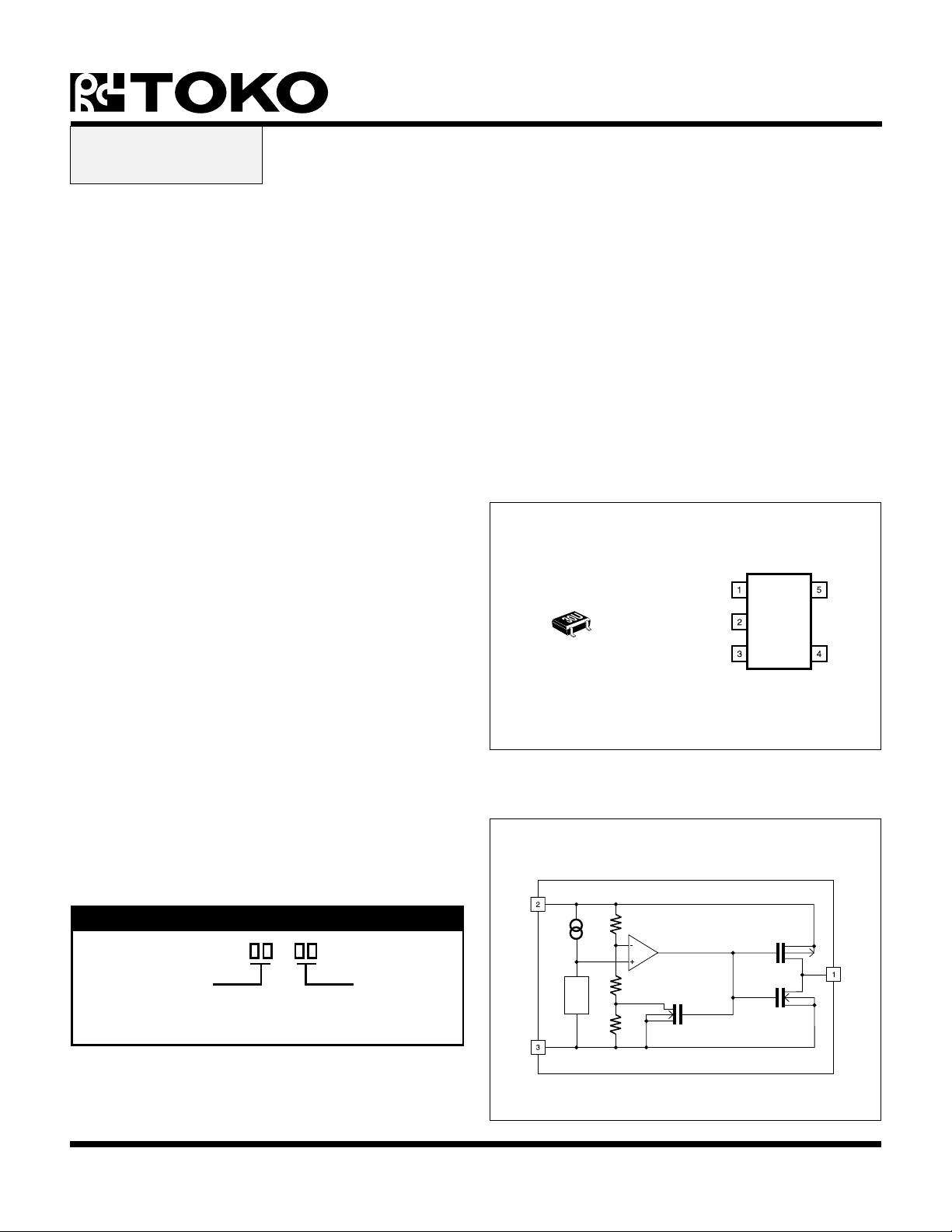
■ Miniature Package (SOT23-5)
DESCRIPTION
The TK610xx family of voltage detectors is designed to
provide accurate monitoring of the battery voltage. These
low powered CMOS devices require no external
components and are available in 0.1 V steps from 2.0 V to
5.0 V.
When the input voltage reaches the detection voltage, the
output goes low. This detection voltage has a ±2 %
accuracy and is set at the factory. When the input voltage
goes high, the output will stay low until the voltage reaches
the detection voltage plus hysteresis (+3 to +7 %).
VOLTAGE DETECTOR
APPLICATIONS
■ Battery Powered Systems
■ Wireless Telephones
■ Pagers
■ Personal Communications Equipment
■ Personal Digital Assistants
TK610xx
OUT
V
DD
GND
NC
NC
The TK610xx is available in a miniature SOT23-5 surface
mount package.
BLOCK DIAGRAM
V
DD
ORDERING INFORMATION
TK610 S
Voltage Code
VOLTAGE CODE *
23 = 2.3 V
25 = 2.5 V
27 = 2.7 V
30 = 3.0 V
33 = 3.3 V
* Consult factory for availability of other voltages
36 = 3.6 V
40 = 4.0 V
41 = 4.1 V
42 = 4.2 V
45 = 4.5 V
Tape/Reel Code
TAPE/REEL CODE
TL: Tape Left
GND
V
ref
October 1999 TOKO, Inc. Page 1
OUT
Page 2

TK610xx
ABSOLUTE MAXIMUM RATINGS
All Pins Except GND ................................................ 11 V
Power Dissipation (Note 4) ................................ 400 mW
Storage Temperature Range ................... -40 to +125 °C
TK610xx ELECTRICAL CHARACTERISTICS
TA = 25 °C, unless otherwise specified.
LOBMYSRETEMARAPSNOITIDNOCTSETNIMPYTXAMSTINU
Operating Temperature Range ...................-30 to +80 °C
Junction Temperature ...........................................150 °C
V
RRE
ycaruccAegatloV1etoN2-2+%
SYHsiseretsyH2etoN 357%
V
HDD
V
LDD
∆V
TED
V
* ∆T
TED
t
RD
I
LSS
I
MSS
I
HSS
I
1NO
I
2NO
I
1PO
egatloVnoitceteD
)L(tnerruCylppuSV
)M(tnerruCylppuS
)H(tnerruCylppuS
egatloVgnitarepOmumixaM9V
egatloVgnitarepOtsewoL 8.0V
tneiciffeoCerutarepmeT
C°03- ≤ pot ≤ C°08001±C°/mpp
emiTyaleDnoitagaporPesiR3etoN001cesµ
DD
V
DD
V
DD
)5etoN()1N(tnerruCtuptuOV
SD
)5etoN()2N(tnerruCtuptuOV
SD
V
SD
)6etoN()1P(tnerruCtuptuO
V0.1=0.1Aµ
,V0.5=
V0.2 ≤ egatloVgnitteS ≤ V0.5
,V0.7=
V2.4 ≤ egatloVgnitteS ≤ V0.5
V,V50.0=
DD
V,V5.0=
DD
V,V1.2=
DD
V8.0=10.050.0Am
V5.1=0.20.4Am
,V5.4=
V0.2 ≤ egatloVgnitteS ≤ V1.4
0.20.4Am
0.10.2Aµ
5.10.3Aµ
V
SD
I
1PO
Note 1: V
Note 2: HYS = 100 * (V
Note 3: The applied voltage is a pulse of V
Note 4: Power dissipation is 400 mW when mounted as recommended. Derate at 3.2 mW/°C for operation above 25 °C.
Power dissipation is 200 mW in Free Air. Derate at 1.6 mW/°C for operation above 25 °C.
Note 5: Output sink current.
Note 6: Output source current.
= 100 * (V
ERR
- Setting Voltage) / Setting Voltage expressed in %
DET
- V
) / V
HYS
DET
expressed in %
DET
LOW
)6etoN()1P(tnerruCtuptuO
= 0.8 V, V
V2.4 ≤ egatloVgnitteS ≤ V0.5
= V
HIGH
DET
+ 2 V
V,V1.2=
DD
,V0.7=
0.60.8Am
Page 2 October 1999 TOKO, Inc.
Page 3
TEST CIRCUIT
TK610xx
OUT VDDGND
FIGURE 1: TEST CIRCUIT FOR V
V
, t
DDL
DR
OUT VDDGND
OV
V
DS
G
V
DD
V
DD
DET
, V
HYS
, V
DDH
OUT VDDGND
V
DD
,
FIGURE 3: TEST CIRCUIT FOR I
OUT VDDGND
OV
V
DS
G
V
DD
SS
FIGURE 2: TEST CIRCUIT FOR I
OP
FIGURE 4: TEST CIRCUIT FOR I
ON
October 1999 TOKO, Inc. Page 3
Page 4

TK610xx
V
V
(V)
2.0
1.5
(µA)
1.0
DD
I
0.5
0.0
0.0 1.0 2.0 3.0 4.0 5.0 6.0 7.0
TYPICAL PERFORMANCE CHARACTERISTICS
SUPPLY CURRENT
VS.
OPERATING VOLTAGE
V
= 4.2 V
DET
VDD (V)
OUTPUT VOLTAGE
OPERATING VOLTAGE
8.0
7.0
6.0
5.0
(V)
4.0
OUT
V
3.0
2.0
1.0
0.0
0.0 1.0 2.0 3.0 4.0 5.0 6.0 7.0
V
DET
= 4.2 V
VDD (V)
VS.
MAXIMUM
OUTPUT SINK CURRRENT
OUTPUT VOLTAGE
20.0
V
15.0
V
10.0
N (mA)
OUT
I
5.0
0.0
0.0 1.0 2.0 3.0
V
DETECTION VOLTAGE AND
HYSTERESIS
4.4
DD
V
= 1.5 V
DD
= 1.0V
DD
V
(V)
DS
VS. TEMPERATURE
4.35
4.3
HYS
4.25
DET
4.2
V
4.15
-50 0 50 100
V
(V)
DD
DD
= 2.0 V
DET
= 2.5 V
V
HYS
VS.
OUTPUT SOURCE CURRRENT
OPERATING VOLTAGE
12.0
V
(V)
DS
V
DS
V
DS
V
DS
V
DS
10.0
8.0
6.0
P (mA)
OUT
I
4.0
2.0
0.0
4.0 6.0 8.0 10.0
V
DD
PROPAGATION DELAY TIME
VS. OUTPUT CAPACITANCE
1
0.1
td (ms)
0.01
0.0001 0.001 0.01 0.1
C
(µF)
OUT
VS.
= 2.5 V
= 2.0 V
= 1.5 V
= 1.0 V
= 0.5 V
tdf
tdr
Page 4 October 1999 TOKO, Inc.
Page 5

DEFINITION AND EXPLANATION OF TECHNICAL TERMS
TK610xx
DETECTION VOLTAGE (V
When V
goes below the detection voltage, the output
DD
DET
)
goes low.
HYSTERESIS VOLTAGE (V
HYS
)
When VDD goes above the sum of the detection voltage
and the hysteresis voltage, the output goes high.
SUPPLY CURRENT (I
SSL
)
Supply current (VDD = 1 V)
SUPPLY CURRENT (I
SSM
)
Supply current (VDD = 5 V) 2.0 V ≤ setting voltage ≤ 4.1 V
SUPPLY CURRENT (I
SSH
)
Supply current (VDD = 7 V) 4.2 ≤ setting voltage ≤ 5.0 V
OUTPUT CURRENT (I
ON1
)
Output sink current of output N channel FET
VDD = 0.8 V, VDS = 0.5 V
MAXIMUM OPERATING VOLTAGE (V
DDH
)
The maximum operating voltage.
LOWEST OPERATING VOLTAGE (V
DDL
)
Voltage when VDD is reduced and output goes up from 0 V
to 100 mV.
DETECTION VOLTAGE TEMPERATURE COEFFICIENT
(∆ V
DET
/ V
DET
* ∆T)
Temperature coefficient of detection voltage.
∆ V
DET
V
* ∆T
DET
RISE PROPAGATION DELAY TIME (t
The delay time for the output to reach (V
when VDD goes from V
1000000 * (V
=
V
LOW
(T) - V
DET
(25 °C) * (T - 25 °C)
DET
DR
= 0.8 V to V
HIGH
(25 °C))
DET
)
+ 2.0 V) / 2
DET
= V
DET
+ 2.0 V
OUTPUT CURRENT (I
ON2
)
Output sink current of output N channel FET
VDD = 1.5 V, VDS = 0.5 V
OUTPUT CURRENT (I
OP1
)
Output source current of output P channel FET
VDD = 4.5 V, VDS = 2.1 V, 2.0 V ≤ setting voltage ≤ 4.1 V
VOLTAGE ACCURACY (V
ERR
)
Error ratio of set voltage
V
= 100 * (V
ERR
- Setting Voltage)/ Setting Voltage
DET
expressed in %
HYSTERESIS (HYS)
Ratio of hysteresis voltage to detection voltage
HYS = 100 * (V
HYS
- V
DET
) / V
expressed in %
DET
October 1999 TOKO, Inc. Page 5
Page 6

TK610xx
V
HYS
V
DET
V
DDL
V
GND
SS
OUTPUT CHARACTERISTICS
V
DD
OUT
Undefined area
OUTPUT vs. SUPPLY VOLTAGE
HYS
(V
V
DET
V
t
DD
DF
+ 2 V
DET
V
DET
+ 2 V) / 2
0.8 V
GND
OUTPUT PROPAGATION DELAY
t
OUT
DR
Page 6 October 1999 TOKO, Inc.
Page 7

APPLICATION INFORMATION
TK610xx
CHANGING DETECTION VOLTAGE USING EXTERNAL
RESISTORS
It is not recommended to set the detection voltage using
external resistors (See figure below) as oscillations may
occur.
OUTPUT H CHARACTERISTICS FOR VDD < V
The output voltage is not defined when VDD < V
V
V
IN
V
DD
V
OUT
G
ND
DD1
.
V
DD
V
HYS
V
DDL
DDL
Note: For the TK610xx , there is an internal diode between
GND and Output and another diode between Output and
V
. Current will flow between these terminals if the diodes
DD
are forward biased. See the figure below for diode polarity.
V
DD
TK610XXS
GND
OUT
t
OUT
V
Undefined
area
t
October 1999 TOKO, Inc. Page 7
Page 8

TK610xx
PACKAGE OUTLINE
SOT23-5
5
1
Marking Information
0.7
Marking
4
1.6
2
3
0.95
e
0.95
e
2.9
+0.15
- 0.05
0.4
1.3 max
+0.1
1.0
2.4
e1
e e
Recommended Mount Pad
0.1
M
1.1
(0.8)
0.95
0.95
Marking
TK61023 23U
TK61025 25U
TK61027 27U
TK61030 30U
TK61033 33U
TK61036 36U
TK61040 40U
TK61041 41U
TK61042 42U
TK61045 45U
0 ~ 15
+0.15
0.1
Dimensions are shown in millimeters
Tolerance: x.x = ± 0.2 mm (unless otherwise specified)
0 - 0.1
- 0.05
0.15
0.3
±
2.8
Toko America, Inc. Headquarters
1250 Feehanville Drive, Mount Prospect, Illinois 60056
Tel: (847) 297-0070 Fax: (847) 699-7864
TOKO AMERICA REGIONAL OFFICES
Midwest Regional Office
Toko America, Inc.
1250 Feehanville Drive
Mount Prospect, IL 60056
Tel: (847) 297-0070
Fax: (847) 699-7864
Western Regional Office
Toko America, Inc.
2480 North First Street , Suite 260
San Jose, CA 95131
Tel: (408) 432-8281
Fax: (408) 943-9790
Eastern Regional Office
Toko America, Inc.
107 Mill Plain Road
Danbury, CT 06811
Tel: (203) 748-6871
Fax: (203) 797-1223
Semiconductor Technical Support
Toko Design Center
4755 Forge Road
Colorado Springs, CO 80907
Tel: (719) 528-2200
Fax: (719) 528-2375
Visit our Internet site at http://www.tokoam.com
The information furnished by TOKO, Inc. is believed to be accurate and reliable. However, TOKO reserves the right to make changes or improvements in the design, specification or manufacture of its
products without further notice. TOKO does not assume any liability arising from the application or use of any product or circuit described herein, nor for any infringements of patents or other rights of
third parties which may result from the use of its products. No license is granted by implication or otherwise under any patent or patent rights of TOKO, Inc.
Page 8 October 1999 TOKO, Inc.
All Rights Reserved
IC-xxx-TKxxxxx
0798O0.0K
Printed in the USA© 1999 Toko, Inc.
 Loading...