

Page 1
TK65010
01S
ADVANCED
INFORMATION
FEATURES
■ Very Low Quiescent Current ( 5 µA)
■ Dual Comparator Outputs
■ Single Monitor Input
■ Miniature Package (SOT-23-5)
DESCRIPTION
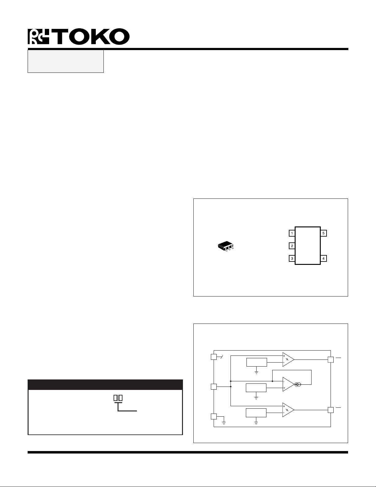
The TK65010 battery voltage monitor is designed for
portable battery powered systems where board space and
cost are important design considerations. The proprietary
monitoring architecture of the TK65010 allows two separate
warning thresholds to be set utilizing a single resistor
divider and single input pin.
The first warning indicator, a Low Battery Output (LBO), is
intended to warn the battery powered system of a low
battery condition. In such a condition, the LBO may be
used to alert the system to illuminate a low battery indicator
and to take appropriate action preparing for battery failure.
BATTERY VOLTAGE MONITOR
APPLICATIONS
■ Battery Powered Systems
■ Cellular Telephones
■ Pagers
■ Personal Communications Equipment
TK65010
V
IN
GND
V
MON
LBO
DBO
The second warning indicator, a Dead Battery Output
(DBO), is intended to be used by the system for shutdown
purposes. The availability of the DBO allows the system to
shut down in order to minimize deep discharge of the
battery.
BLOCK DIAGRAM
The two warning indicators can be implemented utilizing
the TK65010 and only two external components.
V
The TK65010 is available in a miniature 5-pin SOT-23-5
CC
710 mV
LBO
surface mount package.
ORDERING INFORMATION
V
MON
700 mV
TK65010
Tape/Reel Code
TAPE/REEL CODE
TL: Tape Left
GND
690 mV
January 1999 TOKO, Inc. Page 1
DBO
Page 2
TK65010
ABSOLUTE MAXIMUM RATINGS
All Pins Except GND .................................................. 6 V
Power Dissipation (Note 1) .......................................TBD
Storage Temperature Range ................... -55 to +150 °C
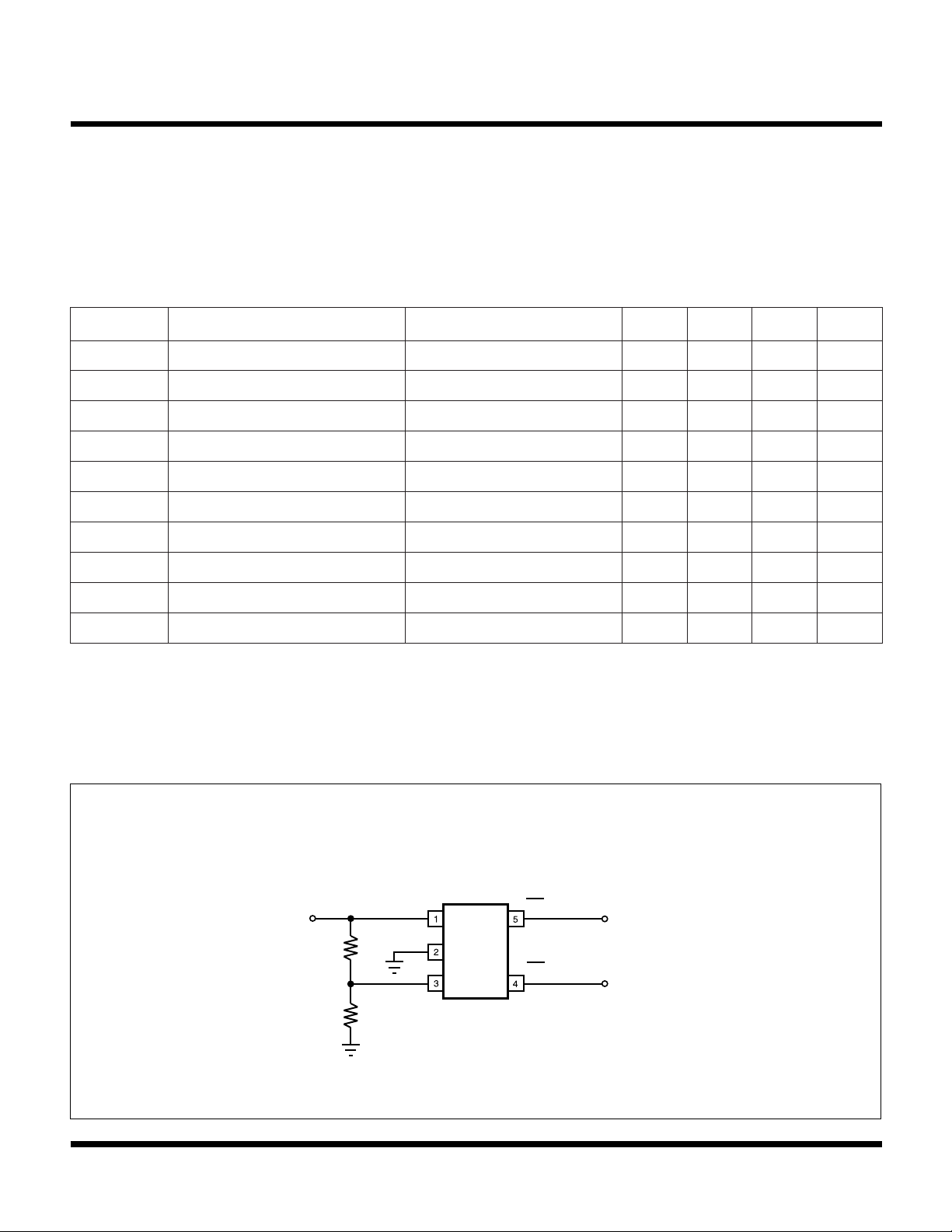
TK65010 ELECTRICAL CHARACTERISTICS
VIN = 5 V, TA = Tj = Full Operating Temperature Range, unless otherwise specified.
LOBMYSRETEMARAPSNOITIDNOCTSETNIMPYTXAMSTINU
Operating Temperature Range ...................-20 to +80 °C
Junction Temperature ...........................................150 °C
V
NI
V
OBL,HT
V
AO,fer
V
OBD,HT
V
V
I
BF
I
Q
V
OBL
V
OBD
Note 1: Power dissipation is 400 mW when mounted as recommended (200 mW In Free Air). Derate at 1.6 mW/°C for operation above 25 °C.
Note 2: When using test circuit below.
TSYH,OBL,HT
TSYH,OBD,HT
egnaRylppuStupnI9.06V
dlohserhTrotarapmoCOBL 017Vm
ecnerefeRpmA-PO 007Vm
dlohserhTrotarapmoCOBD 096Vm
siseretsyHrotarapmoCOBL DBTVm
siseretsyHrotarapmoCOBD DBTVm
tnerruCkcabdeeFkaePV
V=
NOM
OBL,HT
085-An
tnerruCtnecseiuQ 5Aµ
dlohserhTyrettaBwoL)2etoN(1.1V
dlohserhTyrettaBdaeD)2etoN(9.0V
TEST CIRCUIT
V
GND
V
IN
MON
BATTERY IN
R
301 K
R
1 M
1
2
Page 2 January 1999 TOKO, Inc.
LBO
LOW BATTERY
DBO
DEAD BATTERY
Page 3
THEORY OF OPERATION
TK65010
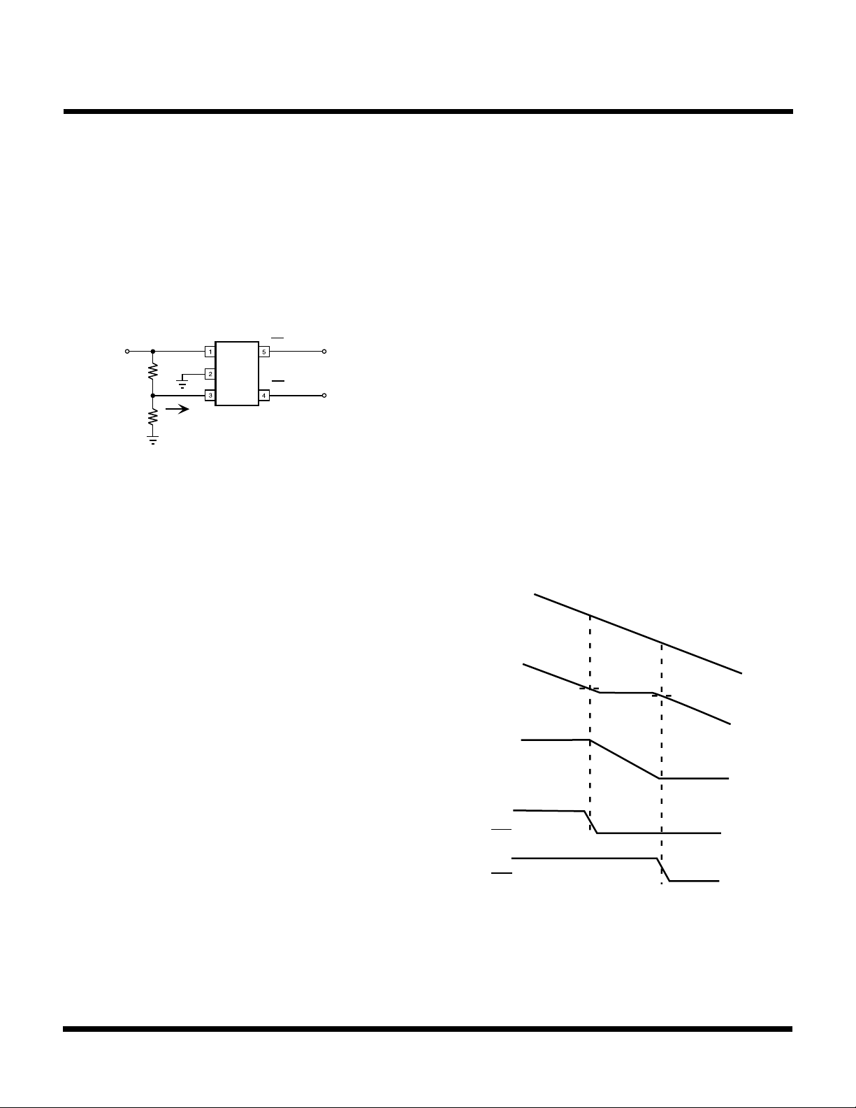
The circuit in Figure 1 illustrates a typical application
utilizing the TK65010. The TK65010 differs from most
voltage monitors due to the fact that two separate
comparator thresholds can be set utilizing a single resistive
divider and a single input pin. One comparator output is
used as an early “low battery” warning. The second
comparator can be used as a later “dead battery” warning.
BATTERY IN
R
301 K
R
1 M
IN
1
2
GND
V
MON
I
FB
LBO
DBO
LOW BATTERY
DEAD BATTERY
V
FIGURE 1
In a typical voltage monitor, which uses an external resistive
divider for setting the voltage monitor threshold, the input
bias current to the monitor pin is essentially zero. In this
type of scenario, the voltage on the monitor input would be
a resistively divided version of the battery voltage. The
TK65010 introduces a small feedback current (IFB) which
introduces a “plateau” into the transfer characteristics
between the battery voltage and the voltage monitoring
pin. The width of this plateau is dependent upon the current
range of the feedback current (IFB) and the values of the
external resistor network. Figure 2 illustrates the typical
relationship between the battery voltage (VIN), the feedback
current (IFB) and the voltage on the monitoring pin (V
MON
Under these conditions, current will be flowing into the
V
pin and will be limited to approximately 580 nA. As
MON
the battery voltage drops, the voltage on the V
drop proportionately. When the voltage on the V
passes through approximately 710 mV, the output of the
first comparator (LBO) will transition from a high to a low
state. Shortly after the LBO output has been asserted, as
the input voltage continues to drop, the magnitude of the
current into the V
pin will begin to proportionately
MON
decrease as the input voltage decreases. An op-amp
feedback loop internal to the TK65010 will attempt to
maintain the voltage on the V
pin at a constant value of
MON
approximately 700 mV (thus, the plateau). As the battery
voltage continues to drop, there comes a point where the
feedback current decreases to approximately zero. A this
point, the voltage on the V
pin will resume a proportional
MON
drop with the input voltage. As the voltage on the V
passes through approximately 690 mV, the second
comparator output (DBO) will be asserted.
For details on how to properly select the resistor divider,
refer to the “Design Considerations” section.
V
LBO
V
IN
V
MON
).
580 nA
700 mV
V
DBO
MON
pin will
pin
MON
pin
MON
In selecting a resistor divider network, there are typically
two degrees of freedom when selecting values. The first
I
FB
0 nA
criteria in selecting the divider is the ratio of the two
resistors. Selecting the ratio defines the lower threshold of
the voltage monitor (DBO). The second degree of freedom
when selecting the resistor divider is the absolute resistance
LBO
values. This second degree of freedom can be utilized to
set a secondary monitoring threshold (LBO) greater than
the first.
DBO
Typically, when the battery voltage is relatively high, the
voltage on the V
divided version of the battery voltage minus the offset. The
pin of the TK65010 will be a resistively
MON
FIGURE 2
magnitude of the offset voltage will be dependent upon the
resistor values comprising the external divider and the
magnitude of the feedback current flowing into the IFB pin.
January 1999 TOKO, Inc. Page 3
Page 4

TK65010
PIN DESCRIPTION
SUPPLY VOLTAGE PIN (VIN)
This pin is the positive power supply for the TK65010.
Current draw from the positive supply is typically 5 µA.
GNOUND PIN (GND)
The pin provides the ground connection for the IC.
VOLTAGE MONITORING PIN (V
This pin is the voltage monitoring pin of the TK65010.
When the voltage on this pin is less than approximately
710 mV, the LBO signal will be asserted. When the voltage
on this pin is less than approximately 690 mV, the DBO pin
will be asserted. This pin is also connected to the negative
input of a high-gain op-amp. The op-amp will attempt to
maintain the voltage on this pin at 700 mV. However, the
current-sink capability of this pin is limited to the range of
0 to 580 nA.
LOW BATTERY OUTPUT PIN (LBO)
This active-low pin will be asserted when the voltage on the
V
pin is less than approximately 710 mV; otherwise the
MON
LBO pin will not be asserted.
DEAD BATTERY OUTPUT PIN (DBO)
This active-low output will be asserted when the voltage in
the V
the DBO pin will not be asserted.
pin is less than approximately 690 mV; otherwise
MON
MON
)
Page 4 January 1999 TOKO, Inc.
Page 5
DESIGN CONSIDERATIONS
TK65010
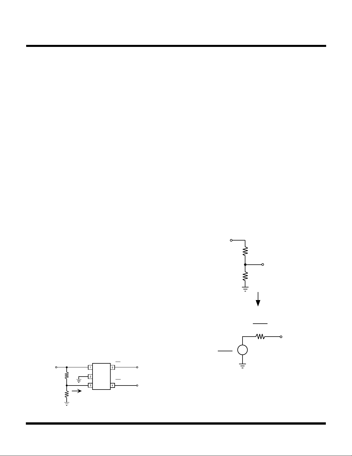
In order to design a voltage monitor utilizing the TK65010,
the two external resistors comprising the resistor divider
must be properly selected. Selecting the ratio of the
resistors will establish the lower monitoring threshold
(DBO). Selecting the value of the R1 will establish the
upper monitoring threshold (LBO) relative to the lower
(DBO) threshold. The value of R2 will be dictated by the
ratio R1/R2 and the value of R1. For the following
explanations, please refer to the circuit diagram of
Figure 3.
SETTING THE DBO THRESHOLD
As mentioned above, the ratio of R1/R2 established the
”dead battery” threshold. The dead battery comparator
trips when the voltage on the V
approximately 690 mV and the current into the V
pin passes through
MON
MON
pin is
approximately zero. Given the required dead battery
threshold, the ratio R1/R2 can be selected utilizing the
following equation:
DBO Threshold = 690 mV x (1 + R1/R2)
or
R1/R2 = (DBO Threshold - 690 mV) / 690 mV
RESISTOR TOLERANCE CONSIDERATIONS
The tolerance of the LBO and DBO thresholds will have a
significant dependence upon the tolerance of the resistive
components used in the resistor divider. When utilizing the
previously described equations for setting the LBO and
DBO thresholds, it is possible that optimal values of the
resistive elements R1 and R2 may be relatively large. Since
large resistive components are not always available with
tight tolerances, an alternate method can be used for
applications where tighter tolerances are required.
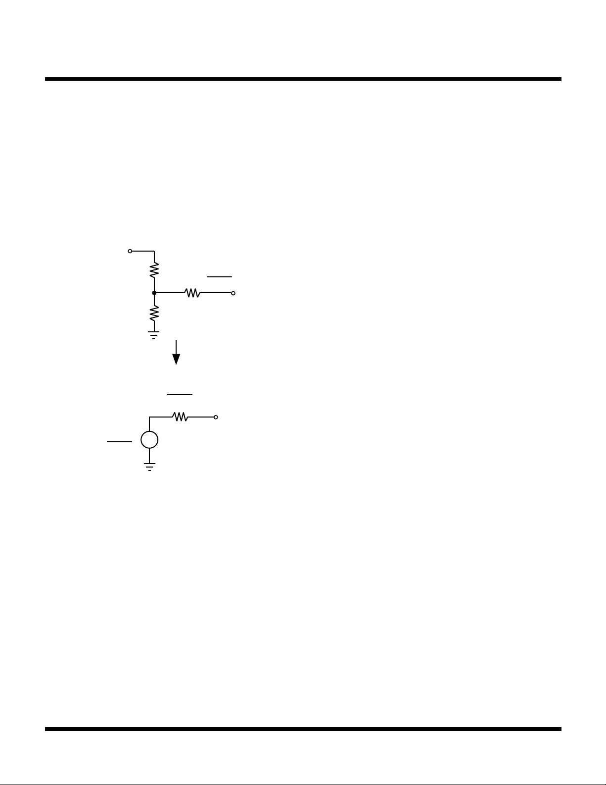
The purpose of the resistor divider connected between the
Battery Input and the V
pin is twofold. The first purpose
MON
is to appropriately select the divider ratio such that the
DBO threshold is set to the desired level. The second
purpose is to select the absolute resistor values such that
the LBO threshold is set to an appropriate level relative to
the DBO threshold. Effectively, an attenuated voltage
source with a relatively large output impedance is driving
the V
pin. This scenario is illustrated in Figure 4.
MON
V
IN
R
1
V
MON
SETTING THE LBO THRESHOLD
R
2
The threshold of the LBO comparator will be at a value
greater than the DBO threshold. The value of resistor
value R1 dictates the difference between the LBO and
DBO thresholds as follows:
LBO Threshold = DBO Threshold x 1.029 + R1 x 580 nA
or
R1 = (LBO Threshold - DBO Threshold x 1.029) / 580 nA
V
BATTERY IN
IN
R
1
R
2
GND
V
MON
I
FB
LBO
DBO
LOW BATTERY
DEAD BATTERY
V
IN
R1 + R
x R
2
2
R1 x R
R1 + R
+
FIGURE 4
2
2
V
MON
FIGURE 3
January 1999 TOKO, Inc. Page 5
Page 6
TK65010
DESIGN CONSIDERATIONS (CONT.)
The resistor divider consisting of R1/R2 can be scaled
downward by a factor scale factor (K) to utilize smaller
resistor values K x R1 and K x R2 (K < 1). By adding an
additional series resistor, which can be dependent upon
the scale factor (K) and the resistor values comprising the
divider, the V
source and drive impedance as illustrated in Figure 4. The
three-resistor attenuator is illustrated below in Figure 5.
pin will effectively see the same voltage
MON
V
IN
V
IN
R1 + R
K x R
x R
2
K x R
1
2
2
FIGURE 5
+
R1 x R
R1 + R
(1- K) x
2
2
R1 x R
R1 + R
V
2
2
MON
V
MON
Page 6 January 1999 TOKO, Inc.
Page 7
Li-ion
CELL
APPLICATIONS INFORMATION
V
IN
V
GND
MON
R
715 K
R
215 K
1
2
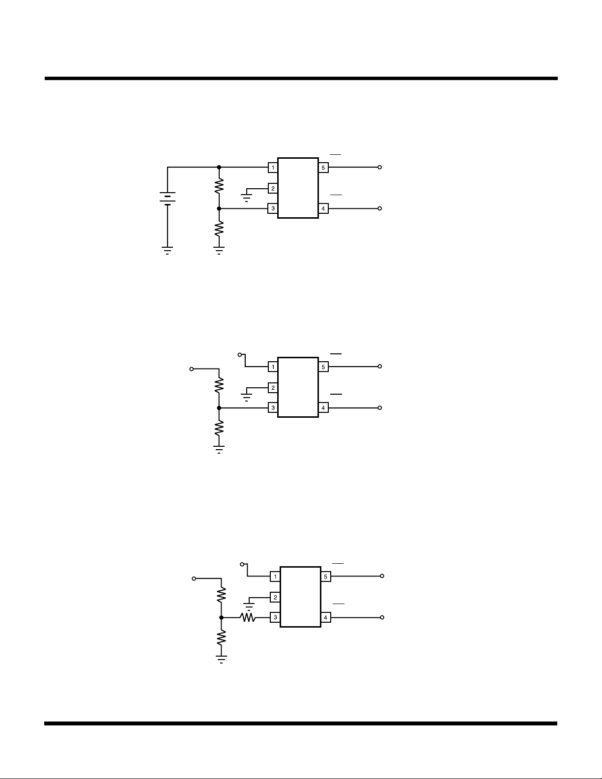
FIGURE 6: BASIC BATTERY MONITOR
LBO
DBO
TK65010
LOW BATTERY
DEAD BATTERY
Low Battery Threshold = 3.5 V
Dead Battery Threshold = 3.0 V
BATTERY
VOLTAGE
BATTERY
VOLTAGE
R
1
1.23 M
R
2
90.9 K
+5 V
V
V
IN
GND
MON
LBO
DBO
FIGURE 7: HIGH VOLTAGE MONITOR
R
1 M
R
2
73.2 K
+5 V
1
13 K
GND
V
V
IN
MON
LBO
DBO
LOW BATTERY
DEAD BATTERY
Low Battery Threshold = 11.0 V
Dead Battery Threshold = 10.0 V
LOW BATTERY
DEAD BATTERY
Low Battery Threshold = 11.1 V
Dead Battery Threshold = 10.1 V
FIGURE 8: HIGH VOLTAGE MONITOR WITH 3-RESISTOR ATTENUATOR
January 1999 TOKO, Inc. Page 7
Page 8
TK65010
)
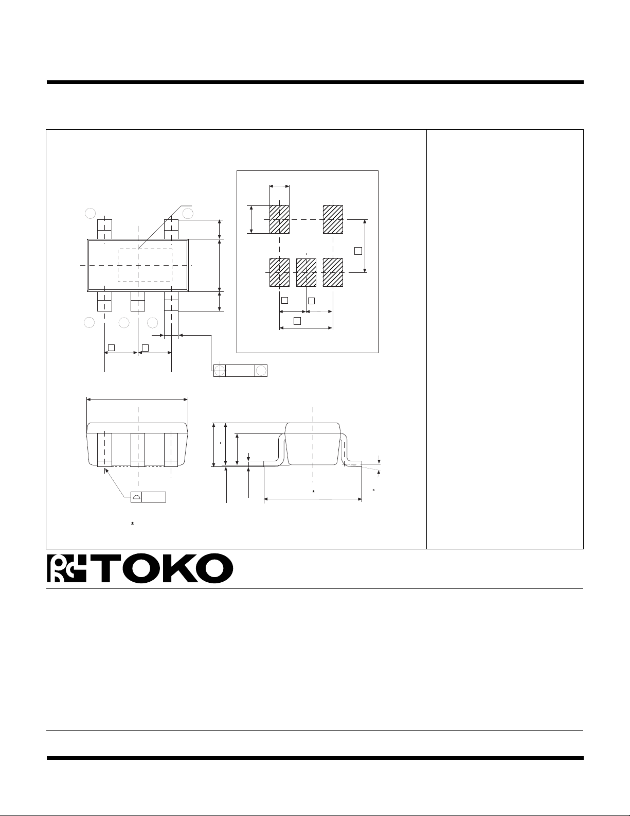
PACKAGE OUTLINE
SOT-23-5
5
1
Marking Information
0.7
Marking
4
(0.6)
1.6
(0.6)
2
3
0.95
e
0.95
e
2.9
+0.15
- 0.05
0.4
1.3 max
+0.1
1.0
2.4
e1
e
e
0.95
0.95
1.90
e'
Recommended Mount Pad
0.1
M
1.1
(0.8)
Marking
TK65010 xxx
+0.15
0.1
Dimensions are shown in millimeters
Tolerance: x.x =
0.2 mm (unless otherwise specified
0 - 0.1
- 0.05
0.15
0.3
2.8
0 - 15 max
Toko America, Inc. Headquarters
1250 Feehanville Drive, Mount Prospect, Illinois 60056
Tel: (847) 297-0070 Fax: (847) 699-7864
TOKO AMERICA REGIONAL OFFICES
Midwest Regional Office
Toko America, Inc.
1250 Feehanville Drive
Mount Prospect, IL 60056
Tel: (847) 297-0070
Fax: (847) 699-7864
Western Regional Office
Toko America, Inc.
2480 North First Street , Suite 260
San Jose, CA 95131
Tel: (408) 432-8281
Fax: (408) 943-9790
Eastern Regional Office
Toko America, Inc.
107 Mill Plain Road
Danbury, CT 06811
Tel: (203) 748-6871
Fax: (203) 797-1223
Semiconductor Technical Support
Toko Design Center
4755 Forge Road
Colorado Springs, CO 80907
Tel: (719) 528-2200
Fax: (719) 528-2375
Visit our Internet site at http://www.tokoam.com
The information furnished by TOKO, Inc. is believed to be accurate and reliable. However, TOKO reserves the right to make changes or improvements in the design, specification or manufacture of its
products without further notice. TOKO does not assume any liability arising from the application or use of any product or circuit described herein, nor for any infringements of patents or other rights of
third parties which may result from the use of its products. No license is granted by implication or otherwise under any patent or patent rights of TOKO, Inc.
Page 8 January 1999 TOKO, Inc.
All Rights Reserved
IC-xxx-TKxxxxx
0798O0.0K
Printed in the USA© 1999 Toko, Inc.
 Loading...