

Page 1
NOISE/SPEECH DISCRIMINATION IN EMISSION ANDRECEPTION
INTEGRATED SIGNAL GAIN COMPRESSOR
IN BOTHMODES
PROGRAMMABLE ATTENUATORS IN BOTH
MODES
ADAPTED TO ACOUSTIC PARAMETERS OF
ALL CABINETS
LOW OPERATINGVOLTAGE2.5V
LOW OPERATINGCURRENT 2.1mA
CHIP SELECT BETWEEN HANDSFREE AND
MONITORINGMODES
TEA7540
HANDSFREECONTROLLER
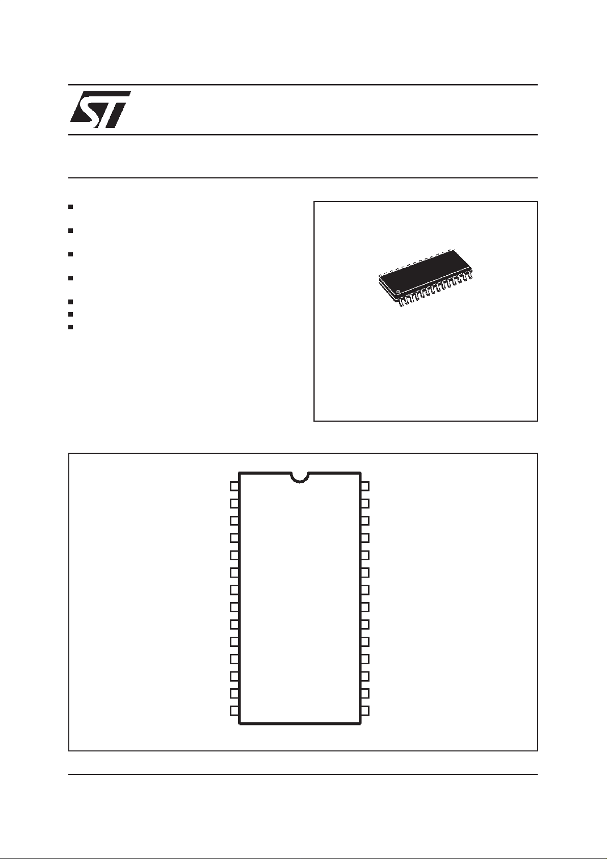
SO28
DESCRIPTION
This 28 pins IC is an innovativeapproach to quality
handsfreetelephonesets.Itresultsfromanextensive
researchonspeechsignal.
PIN CONNECTION
(topview)
HYST1 ATR
HYST2
MICOUT
GND
CS
OUTE
ATTE
TIM
CCE
CE3
CE2
CE1
INE
VREF
1
2
3
4
5
6
7
8
9
10
11
12
13
14
ORDERING NUMBERS:
28
27
26
25
24
22
21
20
19
18
17
16
15
V+
IREF
OUTR
ATTR
VOL23
AMP SUP
AMP IN
CCR
CR3
CR2
CR1
RECOUT
INR
TEA7540FP
D93TL005
July 1998
T is advanced informationon a new product now indevelopment or undergoing evaluation. Details are subject to change without
1/12
Page 2
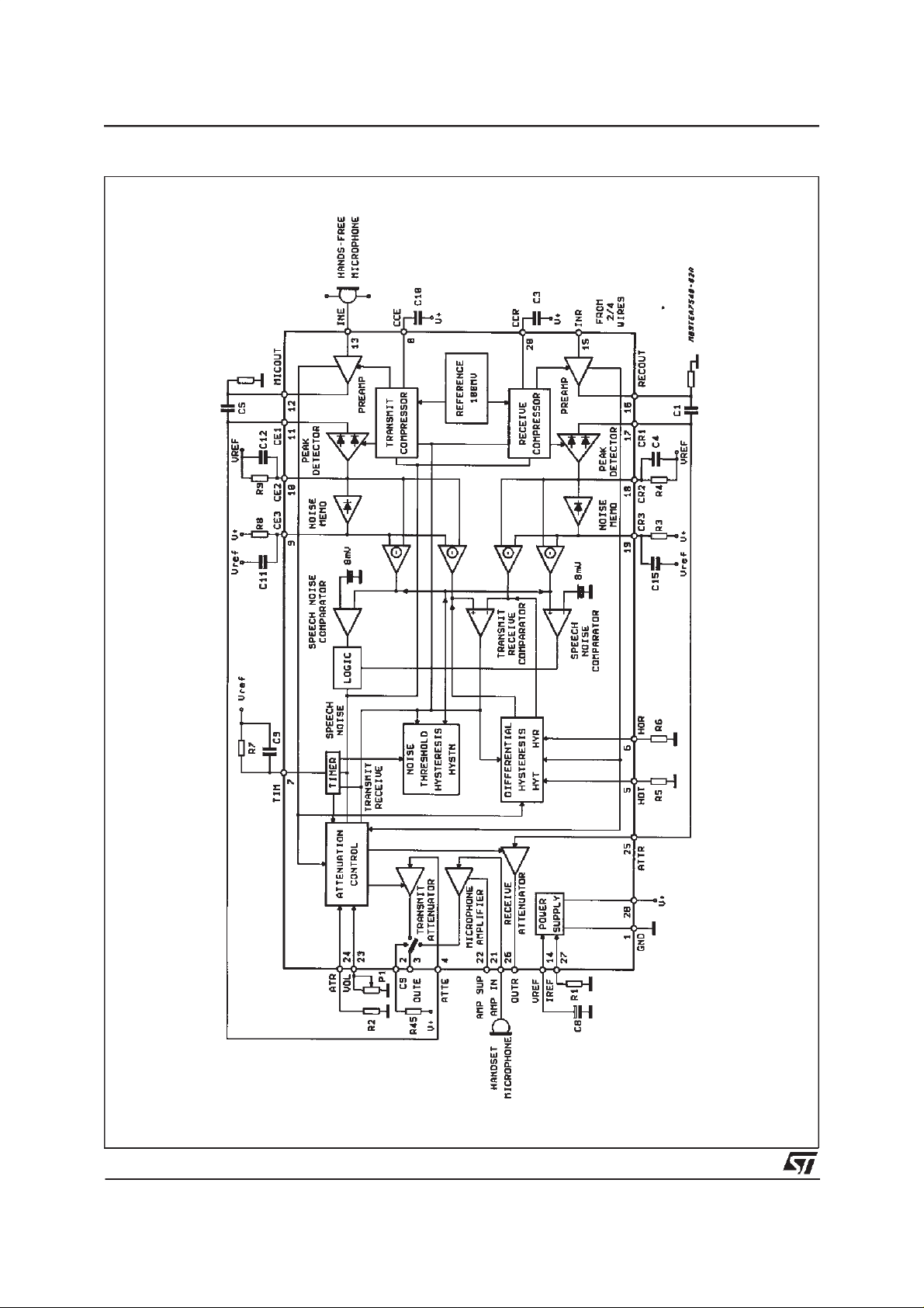
TEA7540
BLOCK DIAGRAM
2/12
Page 3
PIN FUNCTION
N° Name Function
1 GND Ground
2 CS Chip Select
3 OUTE Transmit Attenuator Output
4 ATTE Transmit Attenuator Input
5 HYST1 Transmit Channel Hysteresis
6 HYST2 Receive Channel Hysteresis
7 TIM RC Timer
8 CCE Time Constant of the Transmit Signal Compressor
9 CE3 Transmit Background Noise Memorization Output
10 CE2 Transmit Peak Detector Output
11 CE1 Transmit Rectifier Input
12 MICOUT Transmit Signal Compressor Output
13 INE Transmit Signal Compressor Input
14 V
15 INR Receive Signal Compressor Input
16 RECOUT Receive Signal Compressor Output
17 CR1 Receive Rectifier Input
18 CR2 Receive Peak Detector Output
19 CR3 Receive Background Noise Memorization Output
20 CCR Time Constant of the Receive Signal Compressor
21 AMP IN Handset Preamplifier Input
22 AMP SUP Handset Preamplifier Power Supply
23 VOL Volume Control
24 ATR Attenuation Value
25 ATTR Receive Attenuator Input
26 OUTR Receive Attenuator Output
27 I
28 V+
ref
ref
V+/2 - Reference Voltage
Reference Current Source
TEA7540
FUNCTIONAL DESCRIPTION
SWITCHEDATTENUATORS
Fig.A represents a block diagram of a handsfree
subset with attenuators in signal mode. To prevent the system from howling, the total loop gain,
including acoustic feedback through the housing
and sidetone coupling, must be less than 0dB.
For this purpose, two switchedattenuatorsare inserted in each mode (emission and reception).
The attenuation is shifted from one mode to the
other, resulting from the speech level comparison
between each way.
To prevent the circuit to switch continuously in
one way, the operation of the IC must be fully
symetrical in both ways. This involves signal comparison, attenuationvalue.
GAIN COMPRESSOR
In TEA7540, two signal compressors are inserted
in each mode before the signal comparison, so
the signal coming from each end has the same
level (100mV peak), the losses in each way (for
instance losses resulting from the line length in
receiving mode) are compensatedand the signal
comparison is fully symetrical. The time constant
of each signal compressor decreases 80 times
more quickly than it increases to prevent from
noise increasing between words. The compressing depth is 38dB.
BACKGROUND NOISEDISCRIMINATION
An additional feature provided in TEA7540 is
background noise level discrimination in each
way. The IC stores the background sound level
with a long time constant (3 to 5 seconds depending on an external RC) and compares it with the
incoming signal in order to distinguish a useful
signal (speech) from the background noise. This
background noise memorization is also used to
compensatethe noise in each mode before signal
comparison: the noise level in each mode is sub-
3/12
Page 4

TEA7540
stracted from the incoming signal before the comparison. So very high noise level in one mode
cannot troublethe comparisonbetween the useful
signals.
The result of the comparisonmanages the attenuators in the following way:
- The maximum attenuation is switched on
the mode where the speech signal is the
lowest. The maximum attenuation is fixed
by two external resistor (maximum 52dB).
Figure A
The time constant of the switch is fixed by
the timer via an externalcapacitor.
- When neither party is talking both attenuators are set to a medium attenuation.
Thus each mode is in idle mode. The time
constant of the switch from active mode to
idle mode must be long enough to prevent
from switching to idle mode between two
words (see fig.B). This time constant is
fixed by an externalRC.
Figure B
SPEECH/NOISE
4/12
Em Rec
A max dB
1
0
1
0
0dB
IDLE (A max/2)
D93TL009A
Page 5

TEA7540
TEA7540OPERATION
TEA7540 is powered through an external shunt
regulator (for instance the shunt regulator of the
monitor amplifier TEA7532) or an external zener
diode.
It can work at a very low voltage (2.5V) over the
circuit and it has a low current consumption
(2.1mA).
It’s also possible via the chip select pin (CS) to
Figure C:
ApplicationDiagram (Example of high range telephoneset using TEA7540).
put the handsfree function in standby to use the
circuit in monitoring mode with the handset microphone.
TEA7540 is designed to work with all kind of microphone,including Electret.
TEA7540 also handles the handset microphone
signal (AMP IN) when the system is set to normal
conversationmode.
ABSOLUTE MAXIMUM RATINGS
Symbol Parameter Value Unit
+
V
Top Operating Temperature -20 to 70
T
stg
Supply Voltage 12 V
Storage Temperature Range -65 to 125
°
°
C
C
5/12
Page 6

TEA7540
ELECTRICALCHARACTERISTICS (Refertotestcircuits,T
=25°C;V+=3V;f=1KHzunless otherwise
amb
specified).
Symbol Parameter Test Condition Min. Typ. Max. Unit Fig.
SUPPLY SECTION
+
V
I
TRANSMIT SECTION
COMPRESSOR
Rine Compressor input impedance PIN13 7.5 10.0 14.5 KΩ 1
C
G
1max
G
1min
V
T
I
cce1
I
cce2
V
cce1
V
cce2
PEAK DETECTOR
R
I
ce2
NOISE MEMORIZATION
V1 Maxvoltage drop on pin 9 33 36 45 mV 8
ATTENUATOR
R
ATE- Attenuation=
ATE-active Mode: Active Rpin24 = 11K
ATE-IDLE Mode: Noise Tx, Rx Comp.
RECEIVE SECTION
COMPRESSOR
R
C
G
2max
G
2min
V
micout
R
I
ccr1
I
ccr2
V
ccr1
V
ccr2
Supply Voltage 2.5 7.0 V 1
Current Consumption Vcs = 0
C
Handsfree mode
2.1
3.0
Vcs= N.C.
Monitoring mode
Compressor Range 16.5 dB
R
1.1
1.5
Maximum Gain 40.5 41.5 42.5 dB 2
Minimum Gain 24.0 25.0 26.0 dB 3
Output Voltage PIN12 compressingrange 160 200 240 mVpp 4
O
Transmit Distortion 3.0 % 4
dh
Compressor dacay timecurrent Increasing gain 1.0 1.25 1.5
Compressor rise time current Decreasing gain 65 85 105
Voltage drop PIN8
V
= Vref - Vpin8
cce
Input impedance PIN11 7.5 10.0 14.5 K
inpd
G1max 0 20 mV 2
G1min 175 225 275 mV 3
Rise time current 16 20 24
Input impedance PIN4 7.5 10 14.5 K
ina
20log(Voute/Vatte)
Rpin24 = 11K
Rpin24 = 15KΩ
Ω
46
58
Mode: Inactive Tx, Rx
Comp. Max Gain
0 1.5 3 dB 10
23 dB 11
Rpin24 = 11K
Ω
Ω
Max Gain
Input impedance PIN15 7.5 10.0 14.5 K
inr
Compressor Range 20.5 dB
R
Maximum Gain 35.5 36.5 37.5 dB 2
Minimum Gain 15.0 16.0 17.0 dB 3
Compressor output voltage PIN16 compressing range 160 200 240 mVpp 4
Receive Distortion 3.0 % 4
dh
Compressordecaytime
Increasing gain 1.0 1.25 1.5 µA5
current
Compressor rise time current Decreasing gain 65 85 105
Voltage drop P IN20
Vccr = Vref - Vpin20
G2max 0 20 mV 2
G2min 175 225 275 mV 3
mA
mA
A5
µ
A6
µ
Ω
A7
µ
Ω
dB
dB
Ω
A6
µ
1
1
1
9
1
6/12
Page 7

TEA7540
ELECTRICALCHARACTERISTICS (continued)
Symbol Parameter Test Condition Min. Typ. Max. Unit Fig.
PEAK DETECTOR
R
I
cr2
NOISE MEMORIZATION
V1 Maxvoltage drop on PIN 19 33 36 45 mV 8
ATTENUATOR
Rina Input impedance PIN25 7.5 10 14.5 KΩ 1
ATR- Attenuation=20lg(Voutr/Vatte)
ATR-active Mode: Active Rpin24 = 11K
ATR-IDLE Mode: Noise RX, TX Comp.
ATTENUATION CONTROL SECTION
V
TIME
I
TIME
V
TIMR
I
TIMR
ATRVOL Volume Control 29 32 35 dB 14
MICROPHONE PREAMPLIFIER
R
amp
G
G
Input impedance PIN17 7.5 10 14.5 K
inpd
Rise time current 16 20 24
Mode: Inactive RX, TX
Rpin24 = 11KΩ
Rpin24 = 15K
Ω
46
58
Comp. Max Gain
0 1.5 3 dB 10
23 dB 11
Rpin24 = 11K
Ω
Ω
Max Gain
Tx Mode Att.Voltage 190 250 325 mV 12
TX Mode Att.Current 40 50 70
RX Mode Att.Voltage -325 -250 -190 mV 13
RX Mode Att.Current 40 50 70
Imput impedance PIN21 35 50 70 K
V
mic
2off
= Voute-Vamp in Vcsopen 19 20 21 dB
mic
Compressor Gain
Monitoring Mode
G2 = V
recout/Vinr
Rext between PINs 2 - 28
Rext = open
Rext = 40K
Ω
36.5
16
Ω
A7
µ
dB
dB
A12
µ
A13
µ
Ω
dB
dB
1
9
Figure 1:
BasicConfiguration
Figure2:
V+=3V
pin 7 is forced to transmit mode
pin 11 is forcedto max gain
Input signal on pin 13 VINE= 1.5mVpp
output voltage VMICOUT measured on pin 12
TestConfiguration
G1max = 20log (VMICOUT / VINE)
7/12
Page 8

TEA7540
Figure 3: Test Configuration
V+=3V
pin 7 is forced to transmit mode
pin 11is forced to minimum gain
Input signal on pin 13 VINE = 1.5mVpp
output voltage VMICOUT measured on pin 12
G1min = 20log (VMICOUT / VINE)
Figure4: Test Configuration
V+=3V
pin 7 is forced to transmit mode
Input signal on pin 13 VINE in the compressing range (5mVpp for
example)
output voltage VMICOUT measured on pin 12
Figure 5:
V+=3V
pin 7 is forced to transmit mode
pin 11is forced to maximum gain
TestConfiguration
Figure6: Test Configuration
V+=3V
pin 7 is forced to transmit mode
pin 11 is forcedto minimum gain
8/12
Page 9

TEA7540
Figure 7: Test Configuration
V+=3V
pin 7 is forced to transmit mode
pin 11is forced to minimum gain
Figure8: Test Configuration
V+=3V
pin 7 is forced to transmit mode
pin 11 is forcedto minimum gain
Figure 9: Test Configuration
V+=3V
pin 7 is forced to receive mode
pin 11and pin 17 are forced to maximum gain
Input signal on pin 4 VATTE = 200mVpp
ATE2 = 20log (VOUTE / VATTE) with Rpin24 = 11KΩ
Figure10:
V+=3V
pin 7 is forced to transmit mode
Input signal on pin 4 VATTE = 200mVpp
ATE = 20log(VOUTE / VATTE)
TestConfiguration
9/12
Page 10

TEA7540
Figure 11: TestConfiguration
V+=3V
pin 7 is forced to idle mode after that the two compressor have been
forced at maximum gain by V11 and V17
Input signal on pin 4 VATTE = 200mVpp
Rpin24 = 11K
ATE6 = 20log(VOUTE / VATTE)
Ω
Figure12: TestConfiguration
V+=3V
pin 11 is forcedto 100mV to force the transmit mode
VTIM_E voltage on pin 7
ITIM_E current through the mA
Figure 13: TestConfiguration
V+=3V
pin 17is forced to 100mV toforce the receive mode
VTIM_R voltage on pin 7
ITIM_R current through the mA
Figure14: TestConfiguration
V+=3V
pin 7 is forced to receive mode
Input signal pin 25: VATTR = 200mVpp
Rpin23 = 9KΩ
ATRVOL = 20log(VOUTR/ VATTR)
10/12
Page 11

SO28 PACKAGEMECHANICAL DATA
TEA7540
DIM.
MIN. TYP. MAX. MIN. TYP. MAX.
A 2.65 0.104
a1 0.1 0.3 0.004 0.012
b 0.35 0.49 0.014 0.019
b1 0.23 0.32 0.009 0.013
C 0.5 0.020
c1 45°(typ.)
D 17.7 18.1 0.697 0.713
E 10 10.65 0.394 0.419
e 1.27 0.050
e3 16.51 0.65
F 7.4 7.6 0.291 0.299
L 0.4 1.27 0.016 0.050
mm inch
S8
(max.)
°
0016572
11/12
Page 12

TEA7540
Information furnished is believed to be accurate and reliable. However, STMicroelectronics assumes no responsibility for the consequences
of use of such information nor for any infringement of patents or other rights of third parties which may result from its use. No license is
granted by implication or otherwise under any patent or patent rights of STMicroelectronics. Specification mentioned in this publication are
subject to change without notice. This publication supersedes and replaces all information previously supplied. STMicroelectronics products
are not authorized for use as critical components in life support devices or systems without express written approval of STMicroelectronics.
Australia - Brazil - Canada - China- France - Germany - Italy - Japan - Korea- Malaysia - Malta- Mexico - Morocco - The Netherlands -
Singapore - Spain - Sweden - Switzerland- Taiwan - Thailand - United Kingdom - U.S.A.
The ST logo is a registered trademark of STMicroelectronics
1998 STMicroelectronics – Printed in Italy – All Rights Reserved
STMicroelectronics GROUP OF COMPANIES
12/12
 Loading...