

Page 1
.PROGRAMMABLEGAININ STEPSOF6 dB
.ON/OFFPOSITION
.LOWVOLTAGE
.POWER: 100 mWAT 5 V
DESCRIP TION
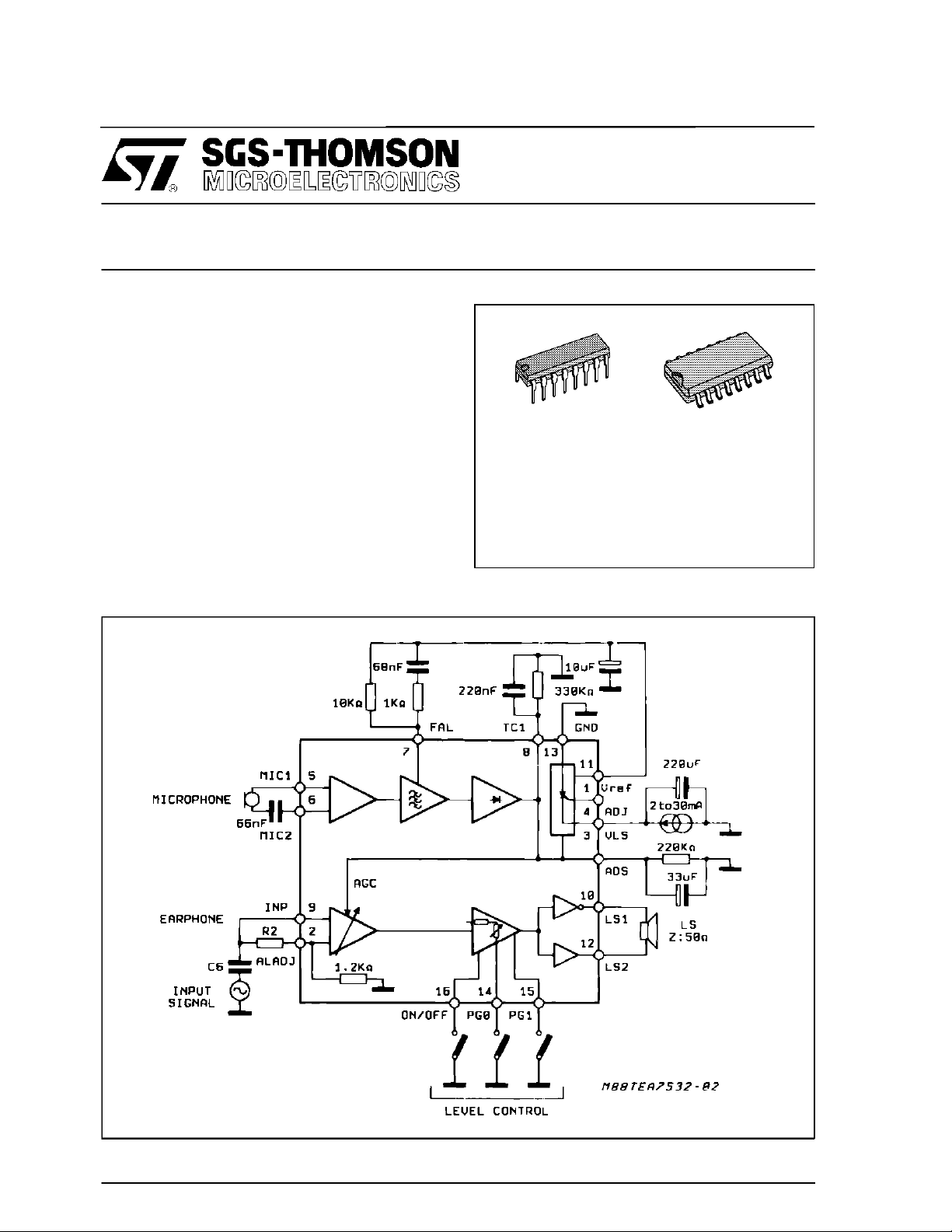
This16 pinsIC is designedfor monitor
(loudspeaker)telephoneset andprovides:
a) Signalamplificationformonitoring(loudspeaker)
b) Antiacousticfeedback(antilarsen)
c)Antidistortionbyautomaticgainadaptation
d) Antilarsenadjustment(full duplex)
BLOCK DI AG RAM
TEA7532
MONITOR AMPLIFIER
DIP 16
ORDERING NUMBERS : TEA7532DP(DIP16)
SO16
TEA7532FP(SO16)
July1993
1/16
Page 2
TEA7532
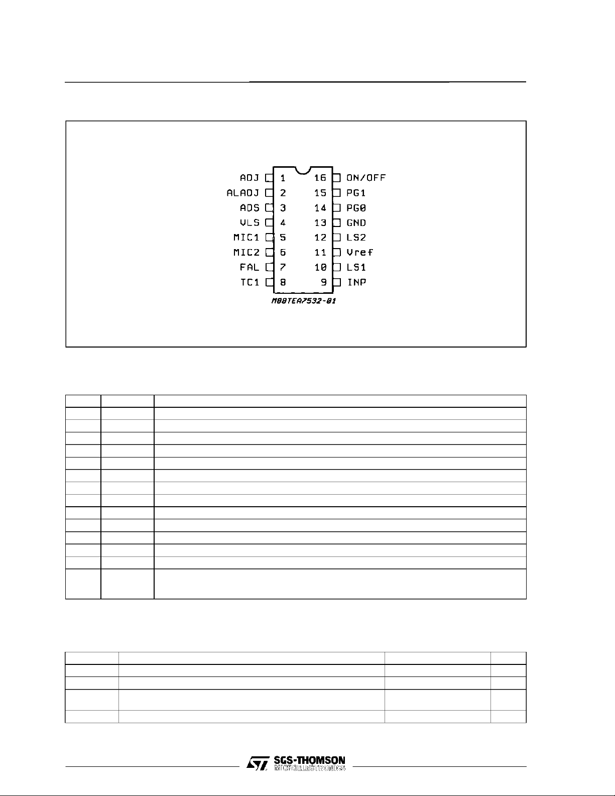
PIN CONNECTI O N (Top view)
PIN DESCRIPTION
N° Symbol Description
1 ADJ Adjust Internal Reference V
LS
2 ALADJ Antilarsen Adjustement
3 ADS Antidistortion
4V
LS
Supply
5 MIC1 Microphone Input
6 MIC2 Microphone input
7 FAL Antilarsen Filter
8 TC1 Antilarsen Time Constant
9 INP Input Signal
10 LS1 Output Loudspeaker 1
11 V
REF
Internal Resistance
12 LS2 Output Loudspeaker 2
13 GND Ground
14
15
16
PG0
PG1
ON/OFF
Inputs Program Level to Loudspeaker
ABSOLUTE MAXIMUM RATINGS
Symbol Parameter Value Unit
T
op
V
LS
I
LS
V
Temperature Range –5 to + 45 °C
Supply Voltage 6 V
Supply Current for T > 300ms
for T ≤ 300ms
Voltage Level (pins, PG0, PG1, on/off) 0.6 > to VS+ 0.6 V
L
90
150
mA
mA
2/16
Page 3
TEA7532
ELECTRICAL CHARACTERISTICS (T
=25oC, ILS= 30mA unless otherwisespecified)
amb
Symbol Parameter Test Conditions Min. Typ. Max. Unit
V
LS1
V
LSM
V
ADJ
G
G000
G001
G010
G011
G100
VLSSupply ILS= 2mA (fig. 7)
= 30mA (fig. 7)
I
LS
VLSMaximum I
=50µA (fig. 7 ; So = closed) 5.5 V
pin 1
Voltage Pin 1 ILS= 2mA to 30mA (fig. 7) 1.1 1.25 1.4 V
V
− V
10
Loudspeaker Amplifier Gain =
12
V
ON/OFF PG0 PG1
9
GND
GND
GND
GND
V
LS
GND
GND
V
LS
V
LS
X
GND
V
LS
GND
V
LS
X
2.6 3.0
12
18
24
30
THD Distortion f = 300Hz to 2kHz,
V
10–V12
G = G011, (fig. 8)
G2 [V(10) – V(12)]/V2 P
Z
MICIN
Z
INPIN
Z
V
OFFS
I
ON/OFF
I
PG0
I
PG1
I
ON/OFF
I
PG0
I
PG1
V
IL ON/OFF
V
IL PG0
V
IL PG1
V
IH ON/OFF
V
IH PG0
V
IH PG1
G
Microphone Input Symetrical at (pins 5-6)
Earphone Input (fig. 9) 2.2 2.8 3.4 kΩ
Antilarsen Adjustment Input 1 1.2 1.45 kΩ
IN2
Ouput Offset
[V
(10)–V(12)
]
Input Current ON State V
Input Current OFF State V
Input Voltage ON State 0.45
Input Voltage OFF State 1.5
Microphone Gain = V
MIC
(7)
/[V
(5)–V(6)
]
Vg Voltage Pin 8 0.48 0.67 0.75 V
G
Loudspeaker Attenuated
ATT
Gain = [V
(10)–V(12)
]/V
(9)
G0=PG1=VLS,V8
Asymetrical at (pin 6) fig. 9
G011 ; (fig. 8) – 50 50 mV
PG1
PG1=VLS
V
MIC
G011 ; V8= 0.6V ; (fig. 10)
G011 ; V
= 0.8V
= 0V ; (fig. 8) – 10
; (fig.8) 1
= 10mV
= 0.4V ; (fig. 10) 20
8
,
RMS
= 0.8V (fig. 8) 30 32 34 dB
–10
–10
1.5
1.5
, f = 2kHz (fig. 10)
RMS
22.5 23.5 24.5 dB
3.4
3.15
3.4VV
14
16
20
22
26
28
32
–30
34
–20
2%
4.5 kΩ
–5
–5
–5
1
1
0.45
0.45
–3030–20 dB
dB
dB
dB
dB
dB
µA
µA
µA
µA
µA
µA
V
V
V
V
V
V
dB
FUNCTIO NAL DESCRIPTI ON
TEA7532performs the followingfunctions:
Thecircuitamplifiesthe incomingsignaland feeds
itto the loudspeaker.PG0andPG1 inputsare used
to set the loudspeakergain in a range of 32dB to
14dBin 6dB steps.
The TEA7532inputs (PG0, PG1, ON/OFF) permit
the loudspeakertobe cut-offthus ensuringprivacy
of communication.
- The antilarsen (antiacousticfeedback)system is
incorporated.
- The maximum power available on a 50Ω impedanceloudspeakeris25mWat3 volts and 100mW
at 5V.
Limitvaluesfor externalcomponents:
R3 min = 5 kΩ (R3 adjustVLS),R7 max= 390 kΩ,
R6 min = R7/35
Rmaxbetweenpin5 and6=10kΩ+C min= 10nF.
3/16
Page 4
TEA7532
Figure 1 : LoudspeakerGain VersusVoltage on
Pin(3) - (8) with Pin2 Open.
(*) ATTENUATION =
Zin2(1.2 K) R2=10K⇒ATT = 20 dB
Zin2(1.2 K) + R2(EX T) R2=3 K⇒ATT ≈ 10 dB
Figure 3 : ACOutput VoltageVersusAmplifier
Gain.
Figure2 :LoudspeakerGain VersusVoltageon
Pin(3) - (8)and VersusR
.(*)
2
Figure4 : Power Availableon Loudspeaker
VersusV
Typical Curve.
LS
Figure 5 : DistortionVersus Output Power. Figure6 : OutputPowerVersusSupplyCurrent.
4/16
Page 5
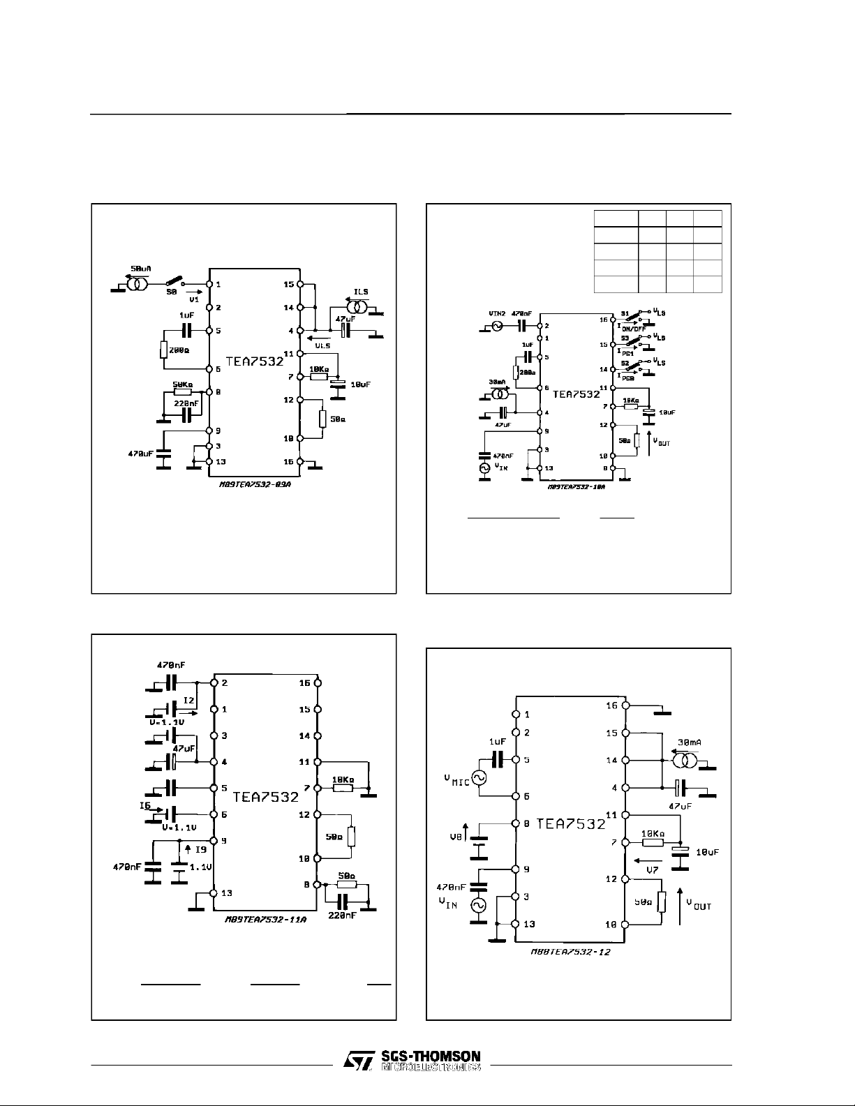
TEST CIRCUI TS
Figure 7 : ShuntvoltageRegulator/Reference
Voltageat Pin 1.
TEA7532
Figure8 : LoudspeakerAmplifier :Gain/Distor
tion/OutputOffset.
S1 S2 S3
G1XX 1 X X
G000 0 0 0
G010 0 1 0
G001 0 0 1
Note : S0 open for VLS 1
S0 close for VLSM.
Figure 9 : ImpedanceZMIC, ZINP andZin2.
V (10)– V (12) V
• G= =
• VOFFS with Vin = 0.
V
LS
G
ND
V (9) V (9)
=1
=0
out
Figure10 : AntiacousticFeedbackSystem at
G011.
Zmic = ; Zinp = ; Zin2 =
1.1V 1.1V 1.1V
I6 I9 I2
5/16
Page 6

TEA7532
CIRCUIT DESCRI PTION
TEA7532isa 16pin DILintegratedcircuitproviding
the following facilities:
Loudspeakeramplifier
-
1.1. LOUDSPEAKERAMPLIFIER
Figure 11.
Antiacousticfeed-backsystem
-
(antilarsensystem)
Theamplifieris dividedinto 3 mainsections.
AutomaticGain Control (AGC)
-
Preamplifier
-
Push-pullamplifier (bridgestructure)
-
a) The AGC section is used for the antilarsenand
antidistortionsystem.
• Whenusedina telephonesettoavoidlarsenef-
fect the AGC automatically decreases loudspeakeramplifiergain.
• When the required output level exceeds the
capabilities of the available current, the AGC
Figure 12.
decreases the loudspeaker amplifier gain to
avoiddistortion.
b) The preamplifier permitsstepcontrolof amplifier
gain in steps of 6 dB, using pins PG0 and PG1,
which maybe controlledusingswitchesor bya microprocessor.Theamplifiermaybemutedusingthe
ON/OFFcontrolsignal (pin16).
c)Theoutputamplifierusesa doublepush-pullconfiguration(Hbridge)togetmaximumdynamicrange
underlimited supplyconditions.
6/16
Page 7

TEA7532
Amplifierdc supply.
Intransmissionmode,the supplyvoltageis controlledby theinternalshunt DC regulator.Forthis reason,theTEA7532shouldbesuppliedfromacurrent
source
Figure 13.
(see: supplyconsiderations).
An antidistortion system is embodied which provides AGC control to avoid loudspeakerdistortion
undercurrent-limitedconditions.
Circuitaction.
Whenthe supplyvoltageis insufficient,thevoltage
at pin1, fallsbelowthereferencevoltage1.1 V,resultingintransistor(TR)beingswitchedoff,resulting
in zero currentflowin resistorR. This stateenables
thegaincontrolsystem.Undertheseconditions,the
shuntDC supplywill switchat a ratedeterminedby
the time constantof theRC network onpin 3.
This switchingactionaccomodatesnormal speech
Figure 14 .
characteristicsunderlow supplyconditions.
1.2. ANTIACOUSTIC FEED-BACK SYSTEM(ANTILARSENSYSTEM)
Thepurposeof thissystemisto controlAGCaction
in order to avoid acoustic feed-back between the
loudspeakerand the microphone, when used in a
telephoneset.
7/16
Page 8

TEA7532
Principle of operation.
When examiningthe spectral density of the voice
area and the larsen area, it can be seen that the
Figure15.
dominant features of each exist in different frequencybands.
To extract the larsen component, the microphone
signalisfirstfilteredbya secondorderfilter(formed
Figure 16.
Zin : 4 kΩ
A= =15
V7
V5 – V6
by two first orderfilters),thenamplifiedand rectified
in orderto producetheAGC control signal.
Thefirst filter is generatedby the capacitorson pins 5 and 6 ; the secondfilterby theR-C network on pin 7.
8/16
Page 9

Figure 17 : AntilarsenSystem FilterResponse.
Filteron pins5 & 6
f2 =
C9 + C10
2π ZinC9 C10
Filteron pin7
f1 =
f3 =
1
2π (R5+ R6)C5
1
2π R5C5
TEA7532
Antilarsensystem
Filter response
If f2 = f3 the Antilarsensystemfilteris equivalent
to a secondorder filter.
C9 +C10 1
2π ZinC9 C10 2π R5C5
=
9/16
Page 10

TEA7532
A complete telephone set has two antilarsen
systems:
one in the transmission circuit(for example :
-
TEA7051)antisidetonenetwork ;
Figure 18.
one in the loudspeakeramplifier
-
(forexample: TEA7532).
Together these form a high efficiency antilarsen
system.
PIN FUNCTI ONS
PIN 1 : ADJUSTV
Thispin is used to adjustthe ICsupplyvoltage.
PIN 2 : ANTILARSENADJUSTMENT
The AC signal at this pin is amplified to the loudspeakerwithout AGCattenuation.
10/16
LS
PIN 3 : AUTOMATICGAINCONTROL FILTER
The antidistortion system responseis adjusted by
the R-C networkon thispin.
TheAGCwillbe switchedON when thelevelon pin
3isgreaterthanthereferencevoltage(0.4V),theRCnetworkcharges(current sourceON) or discharges
(currentsourceOFF)accor dingto thesupplyvoltage.
Page 11

THEORETICAL VOLTAGE ON PIN 3
Figure 19 :
Figure 20.
TEA7532
Thevalue ofR affects the systemtime constant
-
and the charge/dischargeduty cycle.
Thevalueof C onlyaffectsthe systemtimecon-
-
stant.
Rshouldbegreateror equalthan150kΩ forcor-
-
rect AGC operation.
PIN 4 : CIRCUIT SUPPLYVOLTAGE
Withpin1 opencircuit,VLSisinternallystabilizedat
2.8 V.
Whenthe TE A7532isunderAGC control,thevoltage
onthispinvariesslightly(dueto AGCaction).
11/16
Page 12

TEA7532
PIN 5/6 : MICROPHONEINPUTS
Theseare used for antilarsencontrol.
PIN 7 : ANTILARSENFILTER1
Thesecondfilterof the antilarsensystem (1 st filter
: pins 5-6)is formed by the RC networkR5C5.
In order to obtain a secondorder filter for the antilarsensystem, the cut-offfrequencydefinedat this
pin,shouldbe the same as that chosen for the first
filter.
For correct TEA7532 operation R6 and R5 should
be fixed at10 kΩ and 1 kΩ respectively.
PIN 8 : ANTILARSENFILTER2
Thegainandtheresponseofthe antilarsensystem
canbeadjustedrespectivelyby theresistorandthe
capacitoronthispin,accordingtotheacousticcharacteristicsof thetelephoneset.
Thevalueoftheresistorshouldnotexceed390kΩ.
Whenthevoltageonthispin exceedsthe threshold
voltageof 0.4 V, the AGCsystemis enabled.
Figure 21.
PIN 9 : EARPHONEINPUT
Inputfor loudspeakersignal.
PIN 10-12 : LOUDSPEAKEROUTPUTS
Maximumoutput voltage : V
=2VLS-2.5 V (with
pp
a gainof 32 dB).
Maximumoutput current: dependingof the supply
current.
Twoloudspeakerconnectionmethodsarepossible,
usingthe amplifierin either”H” mode or ”B” mode.
Note : It is advisable to connecta 47nF capacitor
in parallel with the loudspeaker (between
pins10 and12).
-”H”Mode
Thisisforlowvoltageworking,butatahighersupply
current.The highestoutputpoweris availableinthis
mode,dueto the 5.5V maximumsupplyvoltagerestriction,imposedby the TEA7532.
Loudspeakerimpedancerecom mendedvalue:50Ω.
Maximum gain available between earphone input
andloudspeakeroutput: 32 dB.
Figure 22.
12/16
Page 13

TEA7532
- ”B” Mode
Thisallowshighervoltageoperation,but at a lower
supplycurrent.
Loudspeakerimpedancerecommendedvalue:25Ω.
Maximum gain available between earphone input
and loudspeakeroutput: 32 - 6 = 26 dB.
Figure 23.
PIN 13 : GROUND
PIN 14-15 : GAINADJUSTMENTINPUTS
Thesepinsare usedto adjustthe loudspeakeramplifier gain.Foursteps of 6 dB/stepare available
(pinopen circuit = high level).
PIN 11 : Vref :INTERNAL REFERENCE
Outputwhich providesaninternallyregulatedreference voltage.
Vref =1.1 V typical
MAXIMUMAVAILABLECURRENT :5 µA
PG0 PG1
1 1 Gmax
1 0 Gmax - <0> 6 dB
0 1 Gmax - 12 dB
0 0 Gmax - 18 dB
PIN 16 : LOUDSPEAKERMUTING.
Thispinis used to mutethe loudspeaker.Pinopen-
circuit: high level= loudspeakermuted.
Pinlow level: louspeakerenabled(see connection
of pins14 and15).
13/16
Page 14

TEA7532
DIP16 PACKAGE MECHANICAL DATA
DIM.
Min. Typ. Max. Min. Typ. Max.
a1 0.51 0.020
B 0.77 1.65 0.030 0.065
b 0.5 0.020
b1 0.25 0.010
D 20 0.787
E 8.5 0.335
e 2.54 0.100
e3 17.78 0.700
F 7.1 0.280
i 5.1 0.201
L 3.3 0.130
Z 1.27 0.050
mm inch
DIP16.TBL
b
Z
16
18
14/16
a1
I
L
Be
e3
D
9
F
b1
E
PM-DIP16.EPS
Page 15

SO16 PACKAGE MECHANICAL DATA
Dimensions
Min. Typ. Max. Min. Typ. Max.
A 1.75 0.069
a1 0.1 0.2 0.004 0.008
a2 1.6 0.063
b 0.35 0.46 0.014 0.018
b1 0.19 0.25 0.007 0.010
C 0.5 0.020
c1 45
D 9.8 10 0.386 0.394
E 5.8 6.2 0.228 0.244
e 1.27 0.050
e3 8.89 0.350
F 3.8 4.0 0.150 0.157
G 4.6 5.3 0.181 0.209
L 0.5 1.27 0.020 0.050
M 0.62 0.024
S8
Millimeters Inches
o
(typ.)
o
(max.)
TEA7532
SO16.TBL
A
a2
b
e
s
e3
D
M
16 9
F
18
GL
a1
c1
b1
C
E
PM-SO16.EPS
15/16
Page 16

TEA7532
Information furnished is believed to be accurate and reliable. However, SGS-THOMSON Microelectronics assumes no responsibility for
the consequences of use of such information nor for any infringement of patents or other rights of third parties which may result from its
use. No license is granted by implication or otherwise under any patent or patent rights of SGS-THOMSON Microelectronics. Specifications mentioned in this publication are subject to change without notice. This publication supersedes and replaces all information previously supplied. SGS-THOMSON Microelectronics products are not authorized for use as critical components in life support devices or
systems without express written approval of SGS-THOMSON Microelectronics.
1994 SGS-THOMSON Microelectronics - All Rights Reserved
Australia - Brazil - France - Germany - Hong Kong - Italy - Japan - Korea - Malaysia - Malta - Morocco - The Netherlands
Singapore - Spain - Sweden - Switzerland - Taiwan - Thaliand - United Kingdom- U.S.A.
SGS-THOMSON Microelectronics GROUP OF COMPANIES
16/16
 Loading...