

Page 1

LOW VOLTAGE
POWER:100mW AT 5V
ANTIDISTORTION SYSTEM FOR LOW CUR-
RENTLINES
TEA7530
MONITORAMPLIFIER
PRELIMINARY DATA
DESCRIPTION
This 8 pins IC is designed for monitor telephone
set andprovides:
a) Signal amplification for monitoring
b) Antidistortionby automaticgain adaptation.
ABSOLUTE MAXIMUM RATINGS
Symbol Parameter
T
V
I
Temperature Range -20 to +70 -20 to +70 °C
op
Supply Voltage 6 6 V
LS
Supply Current for T > 300ms
LS
for T ≤ 300ms
BLOCK DIAGRAM
MINIDIP SO-8
ORDERING NUMBERS:
TEA7530DP TEA7530FP
Value
Minidip SO
90
150
75
120
Unit
mA
mA
June 1993
This is advanced information on anew product now in development or undergoing evaluation. Details are subject to change without notice.
1/11
Page 2
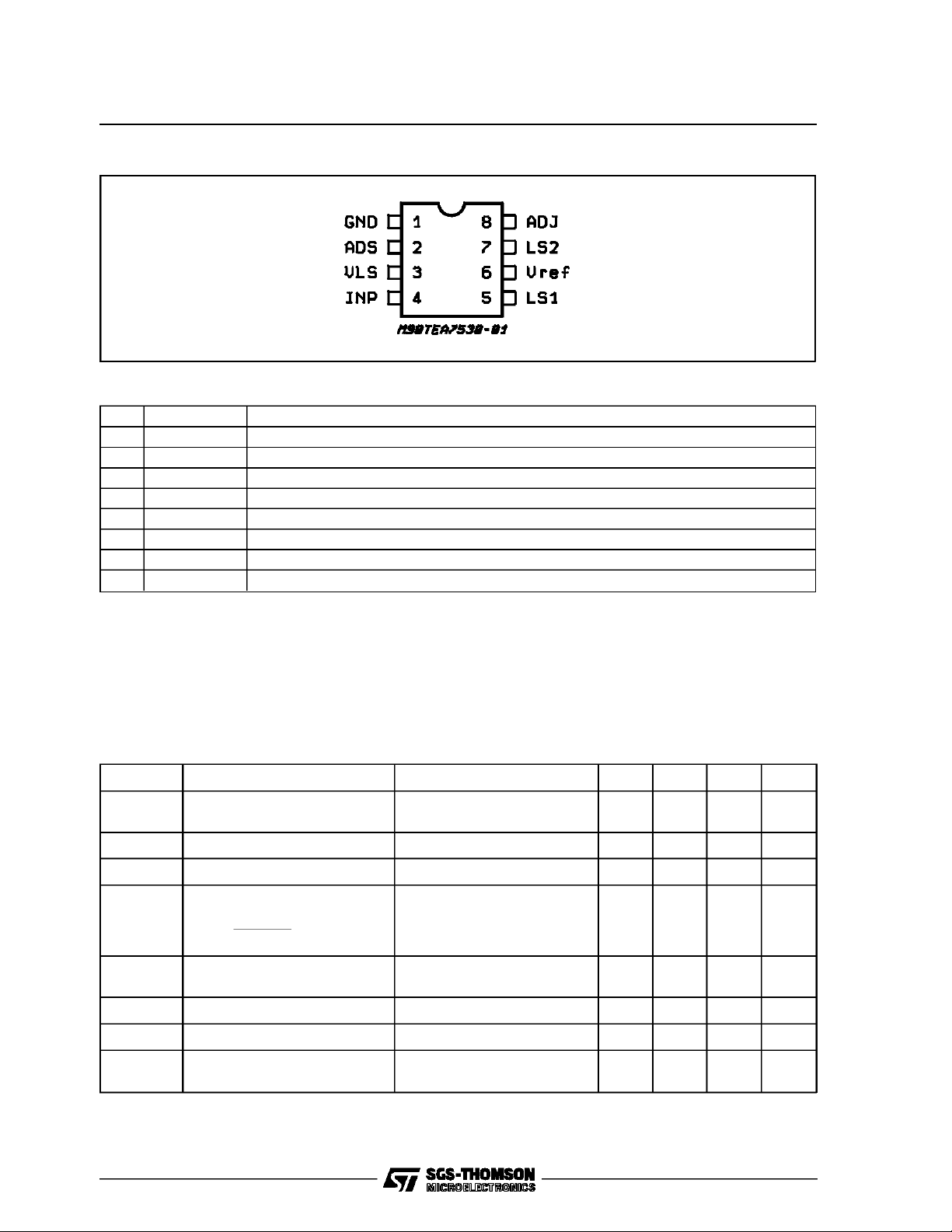
TEA7530
PIN CONNECTION (top view)
PIN FUNCTION
N° Symbol Description
1 GND Ground
2 ADS Antidistortion
3V
LS
4 INP Input Signal
5 LS1 Output Loudspeaker 1
6V
REF
7 LS2 Output Loudspeaker 2
8 ADJ Adjust Internal Reference V
Supply
Internal Reference Voltage
LS
FUNCTIONAL DESCRIPTION
TEA7530performsthe followingfunctions:
The circuit amplifies the incoming signal and
feeds it to the loudspeaker.
ELECTRICAL CHARACTERISTICS (T
=25°C,ILS= 30mA unless otherwise specified)
amb
♦ The Antidistortion system is incorporated for
lowcurrent availablefromline.
♦ The maximum power available on a 50Ω im-
pedanceloudspeakeris 25mW at 3V and 100mW
at5V.
Symbol Parameter Test Condition Min. Typ. Max. Unit
V
LS1
V
LSM
V
ADJ
G Loudspeaker Amplifier
THD Distortion f = 300Hz to 2KHz
Z
INPIN
V
OFFS
GATT Loudspeaker Attenuated
V
Supply ILS = 2mA (fig. 5)
LS1
VLSMaximum I
I
= 30mA (fig. 5)
LS
=40µA (fig. 5; So = closed) 5.7 V
pin8
2.7 3
3.15
3.3
3.4
Voltage Pin 8 ILS= 2 to 30mA (fig. 5 1.0 1.25 1.5 V
ILS= 30mA (fig. 6) 30 32 34 dB
V
− V
(5)
Gain =
(7)
V
(4)
2%
V
(5)-V(7)
= 0.8Vrms; (fig. 6)
Earphone Input (fig. 7) 2.1 2.8 3.5 KΩ
Output Offset [V
Gain = [V
(5)-V(7)
] (fig. 6) -80 80 mV
(5)-V(7)
V
]/V
= 0.7V; (fig. 8)
(2)
V
(4)
= 0.4V; (fig. 8) 20
(2)
-30
30
-20 dB
V
V
dB
2/11
Page 3
TEA7530
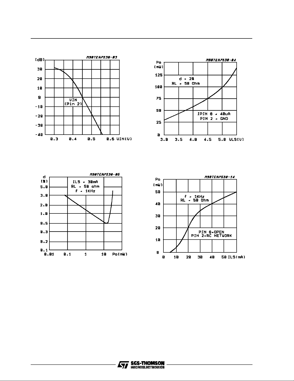
Figure1: LoudspeakerGainvs. Voltage on Pin 2 Figure 2: Power Available on Loudspeakervs.
TypicalCurve. (VoltageMode
V
LS
Figure3: Distortion vs. OutputPower Figure4:
OutputPower vs. SupplyCurrent
(CurrentMode Supply)
3/11
Page 4
TEA7530
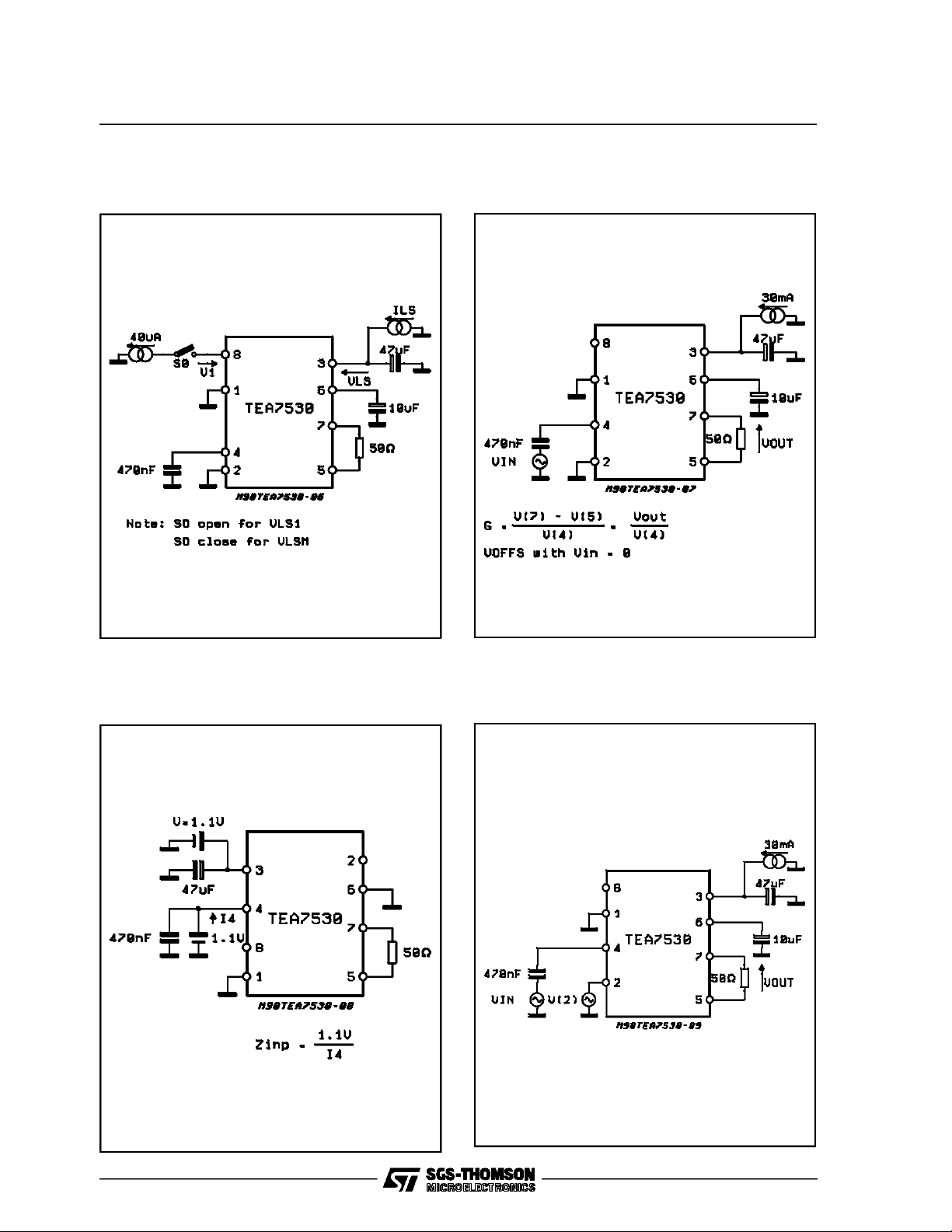
TEST CIRCUITS
Figure5: ShuntvoltageRegulator/ Reference
Voltageat Pin 8.
Figure6: LoudspeakerAmplifier:
Gain/Distortion/OutputOffset
Figure7: Impedance, ZINP
Figure8: Anti-loadingFeedbackSystemat
G = GATT
4/11
Page 5

TEA7530
CIRCUITDESCRIPTION
TEA7530 is a 8 pin DIP integrated circuit providing the followingfacilities:
♦ Loudspeakeramplifier
♦ Antidistortion feed-back system (limited line
currentcompensation)
1.1. LOUDSPEAKERAMPLIFIER
The amplifier is divided into 2 main sections.
- Automatic Gain Control (AGC)
- Push-pull amplifier(bridge structure)
Figure9
a) The AGC section is used for the antidistortion
system.
♦When used in a telephone set to avoid larsen
effect the AGC automatically decreases loudspeaker amplifiergain.
♦When the required output level exceeds the
capabilities of the available current, the AGC
decreases the loudspeaker amplifier gain to
avoidsdistortion.
b) The output amplifier uses a double push-pull
configuration(H bridge) to get maximum dynamic
rangeunder limitedsupply conditions.
Figure10
5/11
Page 6

TEA7530
AmplifierDC Supply
In transmission mode, the supply voltage is controlled by the internal shunt DC regulator. For this
reason, the TEA7530 should be supplied from a
currentsource (see:supply considerations).
An antidistortion system is embodied which provides AGC control to avoid loudspeakerdistortion
under current-limitedconditions.
AGC Circuit action
When the supply V
isinsufficient, the voltage at
LS
pin 8, falls below the reference voltage 1.2V, resulting in transistor (TR) being switched off, resulting zero current flow in resistor R. This state
enables the gain control system. Under these
conditions, the shunt DC supply will switch at a
rate determined by the time constant of the RC
networkon pin 2.
This switching action accomodates normal
speech characteristic under low supply conditions.
The AGC will be switched ON when the level on
Pin 2 is greater than a reference voltage of 0.4V.
SupplyConsiderations
a) Current MODE - Pin 8 is open (V
LS=VLS1
)or
connected to ground with an external resistor
) higher than 16KΩ. The typical value of V
(R
ext
is:
V
= 1.2V
LS
The AGC section is working as described in the
40.5KΩ+(27K
( 27KΩ⁄⁄R
Ω⁄⁄R
EXT
)
EXT
)
.
LS
previousparagraph.
b) Voltage MODE - Pin 8 isshorted or connected
to GND with a resistor(R
) lower than 16KΩ.In
EXT
this condition the circuit must be supplied with a
DC voltage of 3 to 5.5V. In this case the AGC
sectionis permanentlyON. Pin 2 must be shorted
to GND (in voltage mode only) to avoid permanent attenuationof the signal at audioinput
PIN FUNCTIONS
PIN1: GND.
PIN2: AUTOMATICGAIN CONTROL FILTER
The antidistortion system response is adjusted by
the R-C networkon thispin.
The AGC will be switched ON when the level on
pin 2 is greater than a reference voltage of 0.4V,
the RC-network charges (current source ON) or
discharges (current source OFF) according to
supplyvoltage.
Figure11
6/11
Page 7

TEA7530
THEORETICALVOLTAGE ON PIN 2
Figure12
Figure13
- The value of R affects the system time constant and the charge/dischargedutycycle.
- The value of C only affects the system time
constant.
- R should be greateror equal to 150KΩfor correct AGC operation.
PIN3: CIRCUIT SUPPLYVOLTAGE
With pin 8 open circuit, V
is internally stabilized
LS
at3V.
When the TEA7530 is under AGC control, the
voltage on this pin varies slightly (due to AGC action).
PIN4: EARPHONEINPUT
Inputfor loudspeakersignal
Pin 2
7/11
Page 8

TEA7530
PIN 5-7: LOUDSPEAKEROUTPUTS
Maximum outpt voltage: V
gain of 32dB).
Maximum output current: depending of the supply
current.
Figure14
=2VLS- 2.5V (with a
pp
and loudspeakeroutputs: 32dB.
- ”Asymmetrical”Mode
This allows higher voltage operation, but at a
lowersupply current.
Loudspeaker impedance recommended value:
25Ω.
Nominal gain available between earphone input
and loudspeakeroutput: 32 - 6 = 26dB.
Two loudspeaker connection methods are possible, using the amplifier in either symmetrical or
asymmetrical mode.
Note:
It is advisable to connect a 47nF capacitor in parallel with the loudspeaker(betweenpins5 and7).
- ”Symmetrical”mode
This is for low voltage working, but at a higher
supply current. The highest output power is available in thismode, due to the 5.7V maximum supply voltage restriction,imposedby the TEA7530
Loudspeaker impedance recommended value:
50Ω.
Nominal gain available between earphone input
Pin6: V
: INTERNALREFERENCE
ref
Output which provides an internallyregulated referencevoltage.
V
=1.2V typical
ref
MAXIMUM AVAILABLECURRENT: 5µA
Pin8: ADJUSTV
LS
Thispin is used to adjust the IC supply voltage.
Figure15
8/11
Page 9

MINIDIP PACKAGE MECHANICAL DATA
TEA7530
DIM
Min. Typ. Max. Min. Typ. Max.
A 3.32 0.131
a1 0.51 0.020
B 1.15 1.65 0.045 0.065
b 0.356 0.55 0.014 0.022
b1 0.204 0.304 0.008 0.012
D 10.92 0.430
E 7.95 9.75 0.313 0.384
e 2.54 0.100
e3 7.62 0.300
e4 7.62 0.300
F 6.6 0260
i 5.08 0.200
L 3.18 3.81 0.125 0.150
Z 1.52 0.060
mm inch
9/11
Page 10

TEA7530
SO8 PACKAGE MECHANICAL DATA
DIM
mm inch
Min. Typ. Max. Min. Typ. Max.
A 1.75 0.069
a1 0.1 0.25 0.004 0.010
a2 1.65 0.065
a3 0.65 0.85 0.026 0.033
b 0.35 0.48 0.014 0.019
b1 0.19 0.25 0.007 0.010
C 0.25 0.5 0.010 0.020
o
c1 45
(typ.)
D 4.8 5.0 0.189 0.197
E 5.8 6.2 0.228 0.244
e 1.27 0.050
e3 3.81 0.150
F 3.8 4.0 0.150 0.157
L 0.4 1.27 0.016 0.050
M 0.6 0.024
o
S8
(max.)
10/11
Page 11

TEA7530
Information furnished is believed to be accurate and reliable. However, SGS-THOMSON Microelectronics assumes no responsibility for the
consequences of use of such information nor for any infringement of patents or other rights of third parties which may result from its use. No
license is granted by implication or otherwise under any patent or patent rights of SGS-THOMSON Microelectronics. Specifications mentioned in this publication are subject to change without notice. This publication supersedes and replaces all information previously supplied.
SGS-THOMSON Microelectronics products are not authorized for use as critical components in life support devices or systems without express written approval of SGS-THOMSON Microelectronics.
1994 SGS-THOMSON Microelectronics - All RightsReserved
Australia - Brazil - France - Germany - Hong Kong - Italy- Japan - Korea - Malaysia - Malta - Morocco - The Netherlands
Singapore - Spain - Sweden - Switzerland - Taiwan - Thaliand - United Kingdom - U.S.A.
SGS-THOMSON Microelectronics GROUPOF COMPANIES
11/11
 Loading...