

Page 1
LOW-RANGE PHONE DEDICATED CHIP
.
RING
- GENERATION OF 8 MELODYTONES
(Includingthe 3 GermanMelody Tones)
- 4 STEPS DIGITAL CONTROL ON THE AMPLIFIEROUTPUT LEVEL
.
SPEECH
- TRANSM I TGAINEXTERN ALLYADJUST ABL E
- RECEIV IN GGAINEXTER NALLYADJUSTA B LE
- AGCSLOPEEXTERN A LLYPROGRAMM ABLE
- SOFTCLIPPINGON SENDING CHANNEL
- RECEIVE AMPLIFIER FOR PIEZO OR
ELECTRODYNAMIC TRANSDUCER
- +6dB MODE ON RECEIVECHANNEL
- LINE POWER MANAGEMENT
.
DIALING
- DTMF GENERATOR
- LOW DC MASK DURING MAKE PERIOD
THROUGH MICROCONTROLLER SERIAL
BUS INTERFACE
.
MICROCONTROLLER INTERFACE
- 1.79MHzCLOCKOR3.58MHzOSCILLATOR
INPUT
.
MICROCONTROLLER POWER SUPPLY
.
MICROCONTROLLER CONTROL INTERFACE INCLUDING SERIALBUS
.
LINE CURRENT EXTRACTOR FOR SUPPLY
OF EXTERNAL PERIPHERALS
(Plastic Package)
ORDER CODE : TEA7088AFP
PIN CONNECTIONS
SOFT
RECIN
SN
AGC
1
2
3
4
TEA7088A
SO28
28
27
26
25
DTMF
V
REF
V
RMC
DCL
DESCRIPTION
The TEA7088A is a Telephone Analog Front End
device, TAFE, which integrates the three basic
functionsof a standardtelephoneset :
- Speechnetwork,
- DTMF generator,
- Ringer generatoron buzzer.
A complete telephone set can be designed using
TEA7088A associated with a low cost microcontroller.
January 1998
MIC1
MIC2
GTR
V
GND
IVLS
V
V
V
GREC
5
6
7
8
CC
9
10
11
S
12
L
13
MC
14
24
23
22
21
20
19
18
17
16
15
DATA
MSK
OSC
RI
PON
RES
V
RING
BUZ
EAR+
EAR-
7088A-01.EPS
1/17
Page 2
TEA7088A
SPEECH
Thespeech network includes :
- a lownoisetransmitchannel suitablefor anykind
of microphonetransducer. Softclippingon transmit line signal is provided by the chip.
- a low noise receive channel with symmetrical
outputs to be compatiblewith both piezoceramic
and electrodynamicearpiece. An additional 6dB
RINGER
Up to 8 different tones can be generated by the
TEA7088Aringer.The digitalvolume controlof the
ringer can be performed through a specific command(4 steps).A ringindicationsignal is provided
to the microcontroller by the TEA7088A.If more
tones are requested the input RM/MSK allows to
inject tones generatedby the microcontroller.
gain can be inserted in the receive channel
throughsoftware control.
- a linelengthgain control(AGC)withstartingpoint
ofgainregulationfixedat25mAlinecurrent;slope
of gainregulationis externallyadjustablewithone
resistor.AGCcan beremovedbyhardware(maximumgain flat) or by software(-2dBflat).
The phoneimpedanceand sidetone can be tuned
throughexternal networks.
FURTHERADVANTAGES
The microcontroller power supply is provided by the
TEA7088A.Thepowersupplyisspecif i cal l ydesigned
tocopewitha longflas horalonggroundkeyduration.
The TEA7088A is able to supply the necessary
current to an external speakerphone circuit
TEA7540 and loudspeaker amplifier TEA7532
without any additionalcircuitry.
Line current and reset indications are provided to
DTMF GENERATOR
The onboard DTMF generator fullfils the CEPT
requirementswith an externalsinglepole filter.
the microcontrollerby theTEA7088A.
The microcontroller drivesthe TEA7088Athrough
a 2 wires serial interface.
PIN DESCRIPTION
Name Pin N° Description
SOFT 1 Transmit Softclipping Time Constant
RECIN 2 Receiving Input
SN 3 Sidetone Network Input
AGC 4 Line Current Regulation Stop Value
MIC1 5 Microphone Input
MIC2 6 Microphone Input
GTR 7 Transmit Gain Adjustment
V
CC
GND 9 Ground
IVLS 10 Line Current Source Power Supply
V
S
V
L
V
MC
GREC 14 Receive Gain Adjustment
EAR- 15 Negative Earphone Output
EAR+ 16 Positive Earphone Output
BUZ 17 RingerBuzzer Output
VRING 18 Ring Power Supply
RES 19 Reset
PON 20 Power On
RI 21 Ring Indicator
OSC 22 Oscillator Input
MSK 23 Mask, Ring Melody Input
DATA 24 Data Input
DCL 25 DataClock Input
V
RMC
V
REF
DTMF 28 DTMF Filter
2/17
8 Transmit and Receive Part Power Supply
11 Voltage Stabilizer
12 Positive Line
13 Unregulated Microcontroller Power Supply
26 Microcontroller Stabilized Power Supply
27 Reference Voltage (VCC/2)
7088A-01.TBL
Page 3
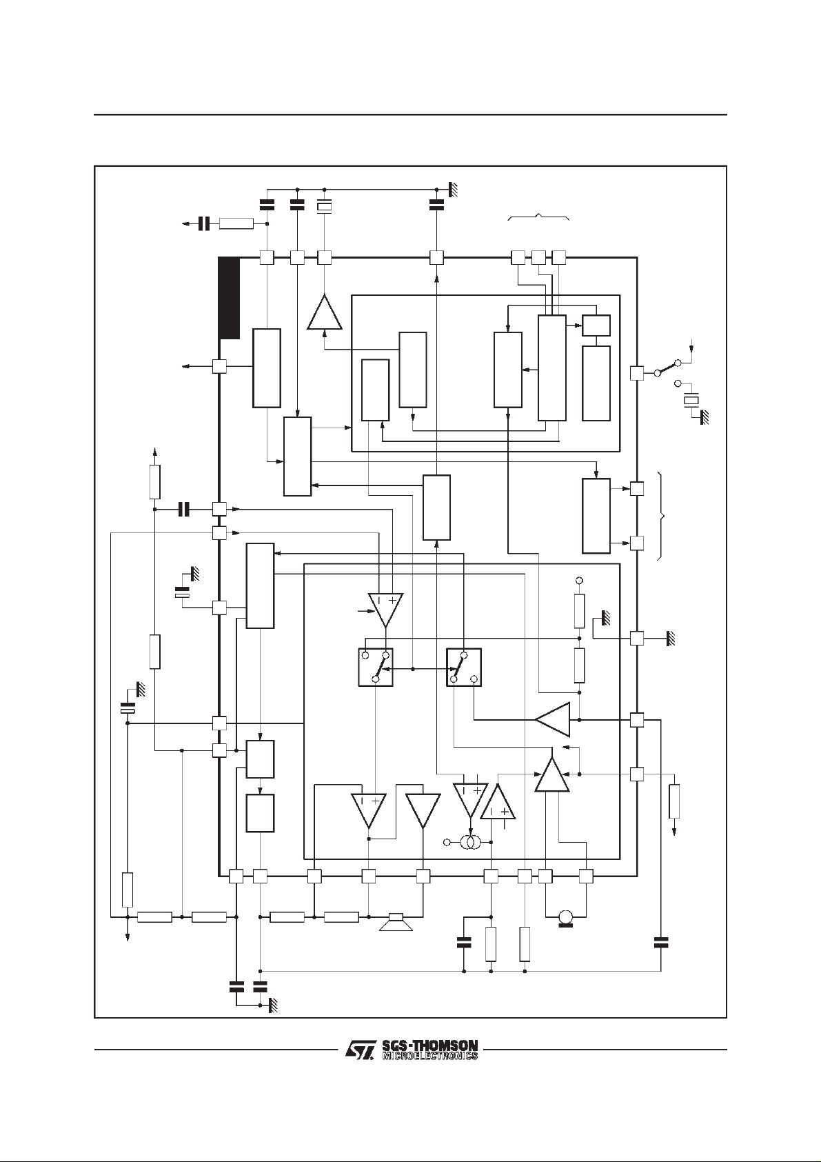
Figure1 : BlockDiagram
TEA7088A
CC
V
Sidetone
R13
C30
To Line
To P
C12
C1
RI
RECIN SN
IVLSV
21
2
C15
C16
R40 + R15
V
18
TEA7088A
SUPPLY
RING POWER
LINE CURRENT
POWER SUPPLY
RMCVRING
26
BUZZER
SUPPLY
LOGIC POWER
BUZ
17
AMPLIFIER
&AGC
SIDETONE
MUTE
AGC
RING
CONTROL
C10
MC
V
13
GENERATOR
SERIAL
REGULATOR
MSK
232425
DTMF
GENERATOR
To P
DCL
DATA
P
INTERFACE
1.79MHz
EXT. CLOCK
OSC
OSCILLATOR /2
3.58MHz
RESONATOR
1920 22
To P
CONTROL
PON & RESET
REF
V
PON RES
GND
9
To Line
C8
R10
R11
V
CC
L
R12
8310
12
V
C11
MUTE
DTMFAGC
28
567
MIC1
AGC
MIC2
Microphone
4
R25
CC
V
C3
C3
KVL
SOFT
R4
IN
V
1
GTR
R8
VSTAB
Earphone
Amplifier
EAR-
Earphone
-1
15
REF
V
11
27
S
REF
V
R14
14
GREC
16
EAR+
R17
C14
7088A-02.EPS
3/17
Page 4
TEA7088A
ELECTRICALCHARACTERISTICS
Theblock diagram is given in Figure 1.
Thevalues of the differentnetworks used in this datasheetare defined as followed:
- The return loss is adjusted by R10 of 600Ω.
- The transmitadjust gainnetworkR8 is calculatedinorder to havea gainof46dB typicalwith I
- The sidetone networkZST is set to be lower than 20dB (Vear/Vmic)on a 600Ωloadon line.
- The DC characteristicsare setby a resistorof 82kΩ betweenV
and VS.
L
Absolute MaximumRatings
Symbol Parameter Value Unit
I
LINE
I
RING
T
T
oper
stg
T
Authorized Voltage on
Pin 2 - RECIN
Pin 3 - SN
Pin 8 - V
Pin 10 - IVLS
Pin 12 - V
Pin 13 - V
Pin 17 - BUZ
Pin 18 - V
Pin 19 - RES
Pin 20 - PON
Pin 21 - RI
Pin 22 - OSC
Pin 23 - MSK
Pin 24 - DATA
Pin 25 - DCL
Pin 26 - V
CC
L
MC
RING
RMC
V
V
V
V
V
V
V
V
RING
RMC
RMC
RMC
RMC
RMC
RMC
RMC
Line Current 120 mA
Ring Current 50 mA
Operating Temperature -25, +70 °C
Storage Temperature -55, +150 °C
Junction Temperature -25, +150 °C
j
13
12
11
6
12
6
+0.3, GND -0.3
27
+0.3, GND -0.3
+0.3, GND -0.3
+0.3, GND -0.3
+0.3, GND -0.3
+0.3, GND -0.3
+0.3, GND -0.3
+0.3, GND -0.3
5
LS
=22mA.
V
V
V
V
V
V
V
V
V
V
V
V
V
V
V
V
7088A-02.TBL
DC Characteristics(T
=25°C; Logic in Default Modeunless otherwise noted)
amb
Symbol Parameter Test Conditions Min. Typ. Max. Unit
V
I
VRMC
V
RMC
I
VMC
I
LS
L
Line Voltage
- In Speech and DTMF Mode
- In Mask Mode
Stabilized Supply Voltage
- Output Current
- Output Voltage IRMC = 1.5mA 3.15 3.35 3.55 V
Unstabilized Supply Voltage
- Start up Current
- Output Current
Line Current Source Supply Test 1, VLS=0V;VMC= 3.6V
Test 1
= 22mA
I
L
= 90mA
I
L
= 22mA
I
L
Test 1, IL= 22mA
V
MC
V
MC
= 22mA
I
L
= 90mA
I
L
= 22mA
L
= 2.5V, I
= 3.6V, I
Test 1, I
VRMC
VRMC
= 1.5mA
= 0mA
4
6.7
4.6
7.5
5.2
8.3
3
1.5 mA
10 15
3
10
67
14
75
18
82
Theline current sourcesupply dependsof IL:
- For I
- For I
Onthis pin the maximumoutput levelis : V
4/17
< 20mA: ILS(mA)= 0.765 x IL(mA)- 1.4mA
L
> 20mA: ILS(mA)= 0.92x IL(mA)- 4.5mA
L
10=V12
- (1.2+ 10 x ILS) and V10<6V
V
V
V
mA
mA
mA
mA
Page 5
TEA7088A
ELECTRICALSPECIFICATIONS(continued)
AC Characteristics(T
Symbol Parameter Test Conditions Min. Typ. Max. Unit
R1 Return Loss Test 2, I
TransmitCharacteristics
(T
=25°C; RL= 600Ω ; f = 1kHz ; Logicin Default Mode unlessotherwisenoted)
amb
Symbol Parameter Test Conditions Min. Typ. Max. Unit
Gtx
Gtxl
Gtxs
Zmic Microphone Input Impedance between MIC1 & MIC2 32 40 48 kΩ
Ntx Noise Test 3, 2kΩ on microphone inputs,
Mmic Microphone Mute Test 3, V
Dtx
V
Max.
L
Microphone Gain Test3, V
Soft Clipping
- Distortion
- Maximum Level on Line
=25°C;RL= 600Ω ; Logic in Default Mode unless otherwisenoted)
amb
= 22mA
f = 300/3400Hz, V
R8 = 1.3kΩ, R25 = 3.9kΩ
I
Test 3, I
L
= -55dBV
m
= 22mA
I
L
= 90mA
I
L
= 22mA
L
= -55dBV, IL= 22mA 60 dB
m
= 22mA, see Figure 2
L
= -41dBV
V
m
= -34dBV 1.5
V
m
= -10dBV
AC
17 dB
4538464047
42
-76 dBmp
2%
dB
dB
Vp
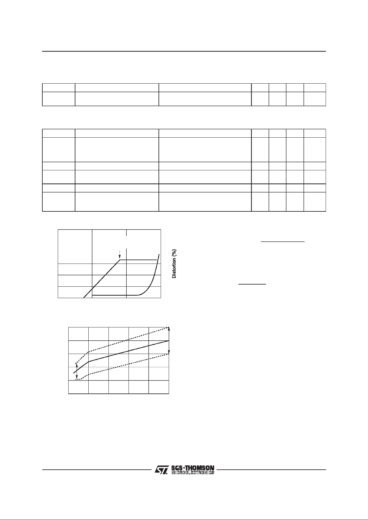
Figure2 : Softclipping
10
Threshold
Level
1
peak on line (V)
AC
V
0.1
0.1 1 10 100
V
microphon e
peak(mV)
Figure3
10
8
6
4
(Pin 12) (V)
L
V
2
VACpeak
0
0 20 406080100
IL(mA)
-15
-10
-5
-2
VACpeak
The maximum gain Gtl is adjustable between 44
and 56dB with R8 :
Gtxl =
20log
820⋅
R10// R
R8 // 50k
+ R11
L
Ω
TheAGCvariationisprogrammedwithoneresistor
connected on Pin AGC. I
is the line current at
SL
whichthe gain must be decreasedby 6dB.
R25 (Ω) =
I
SL
300
− 5mA
For line current lower than I
The transmit and receive gains have a constant
7088A-03.EPS
value.
(R25 > 2.6kΩ)
or higher than ISL,
LL
If no resistor or a resistor higher than 300kΩis
connected on Pin AGC, the gain is constant and
equal to Gtxl and Grxl.±0.5dB.
AGC can be inhibited also through MCU code
”010100”. In this case Tx and Rx gains are fixed
2dB lower than the maximumgain.
The minimumsaturationvoltageof theTEA7088A
respect to ground is 2.2V. On long line, when the
voltage over TEA7088A is low, the softclipping
function automatically limits the AC dynamic to
avoidto reachthe 2.2Vlimiton TEA7088Arespect
7088A-04.EPS
to ground.
5/17
Page 6
TEA7088A
ELECTRICALSPECIFICATIONS(continued)
ReceiveCharacteristics (T
Symbol Parameter Test Conditions Min. Typ. Max. Unit
E
G
G
Dr Distortion Test 4, Rear = 300Ω,I
Nr Noise Test 4, I
Vear
(010010)
Zout Output Impedance 20 Ω
Sidetone
ff
Eff = (Vear
Gain in Symmetric Mode
Grx = (Vear
RXl
RXs
+
- Vear-) /Vm
+
- Vear-)/V
Earphone Mute I
=25°C; RL=660Ω ; f = 1kHz)
amb
Test 3, V
R14 = 10kΩ, R17 = 15kΩ
= -55dBV, IL= 22mA,
m
Test 6, VL= -14.5dBV, R14 = 10kΩ,
L
R17 = 15kΩ, R25 = 3.9k
= 22mA
I
L
= 90mA
I
L
Vear = -12dBV
Vear = -8dBV
= 22mA -76 dBmp
L
= 22mA, VL= -14.5dBV 60 dB
L
Ω
= 22mA
L
0.7
-6 1.7
22.5 dB
2.7
-4
-2
2
5
dB
dB
%
%
Automatic Gain Control Inhibition (T
=25°C; RL= 660Ω; f = 1kHz no AGC mode selected)
amb
Symbol Parameter Test Conditions Min. Typ. Max. Unit
Gtp
Grp
Transmit Gain
Receive Gain
Ring Characteristics (T
amb
=25°C)
Test3 &Test4, I
Code : 010100
= -55dBV
V
m
= -14.5dBV
V
L
= 22to 90mA
L
Gtxl -3
Grxl -3
Gtxl -2
Grxl -2
Gtxl -1
Grxl -1dBdB
Symbol Parameter Test Conditions Min. Typ. Max. Unit
Ringing Threshold Voltage Test 5 a/b
V
Thri ON
V
Thri OFF
I
CRing
V
t
RON
V
RING
V
RMC
Internal Consumption in Ring
Mode
Microprocessor Supply Voltage 3.45 3.75 4.05 V
Rise Time I
Internal Zener Voltage 27 V
Buzzer V
bout
Freq = 1312Hz
out
Freq. Code 001111
Figure4 : RingerHysteresisRinger
ON
RI high (see Figure 4)
Rl low (see Figure 4)
V
= 10V 1 1.2 mA
RING
= 10mA 100 ms
RING
15
5
VRING = 27Vzener (see Figure 5)
Level Code (011111)
Level Code (011110)
Level Code (011101)
Level Code (011100)
12
4.4
2.2
13
5.6
2.8
1
1.4
Figure 5 : Ringer OutputWaveform
20
9
13.5
6.7
3.4
1.8
V
V
V
RMS
V
RMS
V
RMS
V
RMS
6/17
Ringer
Status
OFF
V
OFF
RingerThreshold (V
THRI
V
bout
V
)
V
ON
7088A-05.EPS
7088A-06.EPS
Page 7

TEA7088A
ELECTRICALSPECIFICATIONS(continued)
DTMF Generator(T
Symbol Parameter Test Conditions Min. Typ. Max. Unit
Amf Tone FrequencyAccuracy Test 6 Pin Osc
Llf
Lhf
Low Freq. Group Line Level
High Freq. Group Line Level
Pmf Preemphasis HF/LF +1 +2 +3 dB
t
DON
t
DOFF
Rise Time
Decay Time
Cmf DTMF Confidence Tone :
Earphone level (low freq.)
Earphone level (high freq.)
– - Unwanted Harmonics Level (see Figure 6) ––––
Figure6 : UnwantedHarmonics Level in DTMF
-30
=25°C; RL= 660Ω)
amb
fclock = 1.79MHz oscillator off
or
Resonator :3.58MHzoscillatoron
C13 =100nF, I
= 22mA
L
- 0.4 0.4 %
-10
-8
-8.5
-6.5
-7
-5
5
5
13
17
17
22
21
27
dBm
dBm
ms
ms
mV
mV
-50
-70
Vline (dBm)
-90
100 1k 10k 100k 1M
(Hz)
Figure 7 : Microcontroller Interface
V
MC
13
Batte ry
C10
47 F
V
5.6V
REFI
7088A-07.EPS
V
RING
V
L
I
Speech
I
Start-u p
kIL
18
I(In Ring)
V
(3.4V)
RMC
26
C15
10 F P+LCD
7/17
7088A-08.EPS
Page 8

TEA7088A
MICROCONTROLLER INTERFACE WITH TEA7088A
All inputs can be driven by a Low level max. of
0.1 x V
anda high level min. of 0.9 x V
RMC
Inputs MSK, DCL and DATA have internal pull-up
resistors of 120kΩand input OSC has a internal
pullup of 240kΩ.
Alloutputs can drivea ±1mA typical.
PowerSupply
The microcontroller is power supplied by a 3.4V
regulated supply (V
powersupply (V
MC
) and by an unregulated
RMC
).
The two supplies are connected through a serial
regulator.The unregulatedpower supply(V
aDCvoltageequalto: V
-0.6Vandmustbelower
12
than 6V.It is also possible to connect a battery at
PinV
and use the regulatedoutputat Pin V
MC
to supplya LCD driver.
The current consumption on the serial regulator
hasa typical value of 60µA.
PowerON (PON)
TheTEA7088Ageneratesa poweron signal(PON)
as soonas the voltage on Pin V
2.6V (0.75x V
final)andthe line currentis pre-
RMC
is higher than
RMC
sent.
Note : During the break period in the
loopdisconndect and Flash mode and
during the exchange line break, the power
ONsignalgoesto lowlevel.Maximumdelay
for Pon decay edge after I
goesto zero
Line
is 50ms (with C8 = 47µF, C11 = 1µF,
C27 = 10µF).
Reset
TheTEA7088Ageneratesarise edgeResetsignal
as soon as the logic power supply is higher than
2.6V (0.75x V
RESETremains high until V
RMC
final).
decreasesbelow
RMC
2.5V or the RESET control code is received. In
Ring,RESET is identical to RI output.
Only new positive edge PON, derivedon opening
and closing the line, is forcing the default mode
again. The Reset control code is only active in
speechmode.
RMC
MC
.
)has
RMC
Serial Bus Interface (Dataand Clock)
Theserial bususes 6 bits.Astandard8bit buscan
be used, bits a6 and a7 are nottake in accountby
the TEA7088A.Different typesof codes areused:
a) The Ring Control Code :
- Ring start up
- Outputlevel codes
b) The Operating Code :
- Speech
- Dialing
- Microphonemute
- Earphone/Microphonemute
c) The Data Codes (DTMF, ring frequencies) :
Those data c odes are stor ed inside the
TEA7088Aand are used as soon as the dialing
code or thering start code is received.
d) The Configuration Code :
- AGC / no AGC(toggle)
- No mask / mask(Low DC in ”make”) (toggle)
- Normal gain / normal gain +6dB, on receive
channel(toggle)
- 1.79MHz external clock / 3.58MHz internal
oscillator(toggle)
Those configuration codes are ”Flip-Flop”
codes.
For instance : The first time that the+6dBcode
is sent, the receivegain increases of +6dB.
If the samecode is sent again, the receivegain
goesbackto normalvalue.In thesameway the
3.58MHz internal oscillator can be switched
OFF with a second transmission of the proper
code.
e) The RESET Code :
ResetcodefromtheMCUwillresetinternallogic
of TEA7088A to default mode and will induce
TEA7088Ato generatea ”RESET” status”low”
to the MCU on Pin 19.
Warning : the ”RESET” code deactivates the
serial bus interface which is reactivated only
aftera ”ON-HOOK/OFF-HOOK”sequence.
f) The INITIALIZATION Code :
Initialization code from the MCU will reset the
internallogic of TEA7088Ato default mode, but
theTEA7088Awillnot generatereset command
to the MCU on Pin 19.
8/17
Page 9

MICROCONTROLLER INTERFACE WITH TEA7088A(continued)
Figure8 : Resetand Power ON
Without us ing the RESET Code through the Serial Bus Interface
I
AABCD DE
L
TEA7088A
V
MC
5
2.7
V
RMC
3.4
2.6
PON
RESET
Us in g the RESET Code through the Serial Bus Interface
I
AB CD DEDFA
L
V
MC
5
2.7
t
t
2.5V
t
t
t
t
V
RMC
3.4
2.6
PON
RESET
A:ON-HOOK
B : START UP + SPEECH
C : PULSE DIALING
D : SPEECH or DTMF
E : LINE B REAKEXCHANGE DURATION
F : LINE BREAK EXCHANGE DURATION > t
td: DELAYFIXED BY THE MICROCONTROLLER
d
tdtd
Re se t con trolcod e (010111 )
sent on the serialbus
t
2.5V
t
t
t
7088A-09.EPS
9/17
Page 10

TEA7088A
MICROCONTROLLER INTERFACE WITH TEA7088A(continued)
TheStart Up Conditions of the TEA7088A
Assoon as RESETis highand beforesending any
code the circuit is in the following default configuration:
- Speech
- No mask
- AGC ON in transmit and receive channels
- Normalgain on receivechannel
- 1.79MHz input clock(oscillator in stand by)
microcontroller through thehigh voltage stage.
The ”MAKE” voltage over the TEA7088A during
dialing can be reduced by sending the mask code
0010101.To recoverthe normalspeech voltageat
the end of dialing the mask code must be sent
again.
If the mask code is not used the voltage over the
TEA7088Aduring dialingis the same asin speech
mode.
6 bit Codes
Between two DTMF or ring frequencies, introducing a Mute or speech code implies to wait 1ms to
end the sinewaveor square period.
DTMF Dialing
To dial in DTMF the following sequence of codes
must be sent :
DTMF Frequencycode : 00XXXX
DialingMode code : 010001
Muteor SPEECHcode : 010010 or010000
The duration of the DTMF signal is fixed by the
delay between Dialing mode code and MUTE or
SPEECHcode.
PulseDialing
The pulse dialing function is performed by the
Figure9 : DATA/CLOCKTiming
t1 t2 t4 t5
t3 t3t0
CLK Data
Data
a0 a1 a 2 a3 a4 a5 a6
Ring Indicator(RI)
In ring mode TEA7088A generates a high logic
levelon PinRI as soonas thevoltageon PinV
ishigherthan V
on V
is higher than3.4V.
RMC
When the voltage on V
ON(19VTyp.),andthevoltage
THRI
becomes higher than
RMC
RING
2.6V,RESET signal becomes also high.
Mask Input (MSK)
MSK inputmust be high by default (Figure 10).
In speech configuration forcing MSK input to low
level will have same functionality than the MASK
code.
For ring mode when it is necessaryto send other
frequenciesthanthe 8basicones,this inputallows
to drive the buzzer output.
Synchro
Figure10 : MASK Timing
I
L
MSK
10/17
Datas with a Change During CLK= 1
PULSE MODE OTHER MODES OTHER MODESFLASH MODE
t0, t1, t2, t3, t4, t5 > 1µs
7088A-10.EPS
7088A-11.EPS
Page 11

MICROCONTROLLER INTERFACE WITH TEA7088A(continued)
Codes
a5 a4 a3 a2 a1 a0
0
0
0
0
0
0
0
0
0
0
0
0
0
0
0
0
0
0
0
0
0
0
0
0
0
0
0
0
010101 Mask/No Mask
010110”+6dB” Normal/+6dBon Receive Channel
010111 Reset Pin Control
111010 Initialization Code
010100 AGC/NoAGC
101000 1.79MHz Ext Clock & Oscillator Stand by /
011100 MinimumRing Level (level 1)
011101 Intermediate Low Ring Level (level 2)
011110 Intermediate High Ring Level (level 3)
011111 Maximum Ring Level (level 4)
0
0
0
0
0
0
0
0
0
0
0
0
0
0
0
0
0
0
0
0
0
0
0
0
1
1
1
1
0
0
0
0
0
0
0
0
1
1
1
1
1
1
1
1
0
0
0
0
1
1
1
1
0
0
0
0
0
0
0
0
1
1
1
1
0
0
0
0
1
1
1
1
0
0
0
0
1
1
1
1
0
0
0
0
0
0
1
1
0
0
1
1
0
0
1
1
0
0
1
1
0
0
1
1
0
0
1
1
0
0
1
1
Keyboard Remarks
0
1
0
1
0
1
0
1
0
1
0
1
0
1
0
1
0
1
0
1
0
1
0
1
0
1
0
1
”2”
”1”
”A”
”3”
”8”
”7”
”C”
”9”
”5”
”4”
”B”
”6”
”0”
”*”
”D”
”#”
1336Hz + 697Hz
1209Hz + 697Hz
1633Hz + 697Hz
1477Hz + 697Hz
1336Hz + 852Hz
1209Hz + 852Hz
1633Hz + 852Hz
1477Hz + 852Hz
1336Hz + 770Hz
1209Hz + 770Hz
1633Hz + 770Hz
1477Hz + 770Hz
1336Hz + 941Hz
1209Hz + 941Hz
1633Hz + 941Hz
1477Hz + 941Hz
822Hz Ring Signal
744Hz Ring Signal
1005Hz Ring Signal
909Hz Ring Signal
1187Hz Ring Signal
1074Hz Ring Signal
1451Hz Ring Signal
1312Hz Ring Signal
Speech Mode
Dialing Mode or Ring Start
Earphone & Microphone Mute
Microphone Mute
3.58MHz Ceramic (toggle)
TEA7088A
In DTMF
Dialing
In Ring
Mode
7088A-03.TBL
11/17
Page 12

TEA7088A
Figure11 : Test Circuits- Test 1(VL/V
100 F
I
L
600
V
REF
560k
Ω
100nF
100nF
10 F
47nF
Ω
47 F
10 F
100 F
47
10 F24V
C2
4.7nF
620
V
CC
3.9kΩ
4
AGC
1
SOFT
26
V
RMC
28
DTMF
27
V
REF
13
V
MC
Ω
17
BUZ
18
V
RING
RMC/VMC
Ω
/ IVMC / ILS)
33
Ω
13V
82kΩ
1.6kΩ
Sidetone
15kΩ
1 F
100nF
RECIN
11 12
S
V
L
V
GTR
GREC
EAR+
SN
7
14
16
8
23
CC
V
TEA7088A
2.2 F
15
DCL
DATA
MSK
OSCRIPON
EAR-
MIC2
MIC1
IVLS
RESET
GND
19202122232425
9
2k
Ω
6
470nF
5
1N4148
10
I
47 F
LS
15k
300
1.3k
10k
V
CC
V
REF
Ω
Ω
Ω
Ω
V
CC
Figure12 : Test 2 (R1)
I
AC
100 F
12/17
I
L
V
Z=
REF
560k
100nF
100nF
10 F
47nF
24V
V
AC
I
AC
V
AC
47 F
Ω
C2
4. 7nF
10 F
100 F
47
Ω
10 F
RI = 20 log
620
V
Ω
CC
1 F
3.9kΩ
13V
RECIN
TEA7088A
DATA
MSK
11 12
S
V
OSCRIPON
4
1
SOFT
26
V
28
DTMF
27
V
13
V
17
BUZ
18
V
RMC
REF
MC
RING
V
CC
DCL
23
8
AGC
Z + 600
Z - 600
33
82kΩ
7088A-12.EPS
Ω
1.6kΩ
Sidetone
15kΩ
V
CC
100nF
15k
300
1.3k
10k
V
REF
Ω
Ω
Ω
Ω
L
V
GTR
GREC
EAR+
SN
7
14
16
2.2 F
15
EAR-
MIC2
2k
Ω
6
470nF
5
MIC1
1N41 48
10
IVLS
RESET
GND
19202122232425
9
I
LS
47 F
V
CC
7088A-13.EPS
Page 13

Figure13 : Test 3 (Gtl / Gts / Zmic / Nt / Mmic/ Dt / Vlmax/ Eff)
33
Ω
0
F
10
I
L
600
V
REF
560k
Ω
100nF
Ω
47 F
C2
4.7nF
620
V
Ω
CC
13V
1
82kΩ
F
3.9kΩ
23
4
1
26
F
10
8
CC
AGC
V
SOFT
V
RMC
RECIN
11 12
S
V
100nF
28
DTMF
27
V
10 F
100
REF
13
V
F
47
Ω
MC
17
BUZ
TEA7088A
47nF
18
V
RING
V
V
12
12
DCL
(010000)
(010011)
DATA
MSK
Eff = 20 log
OSCRIPON
V
ear
V
m
19202122232425
Gtl/Gts = 20 log
V
12
V
m
10 F24V
Mmic = 20 log
Figure14 : Test 4(Grl / Grs/ Dr / Mear/ Nr)
13V
1 F
11 12
S
V
MSK
OSCRIPON
33
82k
Ω
Ω
V
19202122232425
I
AC
I
L
V
REF
560k
100nF
100nF
10 F
47nF
24V
Grl/Grs = 20 log
100 F
V
AC
47 F
Ω
10 F
100 F
47Ω
10 F
V
ear
V
12
C2
4.7nF
620
V
Ω
CC
3.9kΩ
23
8
RMC
REF
MC
RING
V
CC
DCL
RECIN
DATA
AGC
4
1
SOFT
26
V
28
DTMF
27
V
13
V
17
BUZ
18
V
TEA7088A
1.6kΩ
Sidetone
15kΩ
100nF
L
V
GTR
GREC
SN
7
14
15k
16
EAR+
300
F
2.2
15
EAR-
6
MIC2
2kΩ
Vm
470nF
5
MIC1
10
IVLS
RESET
GND
9
1.6k
Sidetone
Ω
1N4148
I
47 F
LS
15k
Ω
100nF
L
GTR
GREC
SN
7
14
15k
16
EAR+
300
2.2 F
15
EAR-
MIC2
2k
Ω
6
470nF
5
MIC1
1N4148
IVLS
RESET
10
GND
9
I
47 F
LS
1.3k
10k
1.3k
10k
TEA7088A
V
CC
V
REF
Ω
Ω
Ω
V
Ω
ear
V
CC
7088A-14.EPS
V
CC
V
REF
Ω
Ω
Ω
V
ear
Ω
V
CC
7088A-15.EPS
13/17
Page 14

TEA7088A
Figure 15 : Test 5a(V
47 F
V
REF
560k
Ω
100nF
100nF
10 F
V
47nF
bout
thri
24VV
thri
10 F
100 F
10 F
)
33
Ω
Sidetone
Ω
15k
Ω
SN
7
GTR
14
GREC
15k
16
EAR+
300
2.2 F
15
EAR-
2k
Ω
6
MIC2
470nF
5
MIC1
1N4148
10
IVLS
GND
47 F
1.3k
10k
Ω
V
CC
V
REF
Ω
Ω
Ω
V
CC
47
C2
4.7nF
Ω
620
V
3.9k
Ω
CC
Ω
8
23
4
AGC
1
SOFT
26
V
28
DTMF
27
V
13
VMC
17
BUZ
18
V
RMC
REF
RING
V
CC
DCL
RECIN
DATA
13V
82k
1 F
11 12
S
V
TEA7088A
MSK
OSCRIPON
1.6k
Ω
100nF
L
V
RESET
9
19202122232425
Figure16 : Test 5b(V
V
REF
560k
100nF
100nF
10 F
47nF
V
bout
I
RING
bout
47 F
Ω
)
10 F
100 F
10 F
C2
4.7nF
620
V
Ω
CC
3.9kΩ
8
RMC
REF
MC
RING
V
CC
DCL
4
AGC
1
SOFT
26
V
28
DTMF
27
V
13
V
47
Ω
17
BUZ
18
V
33
Ω
13V
1 F
82k
1.6k
Ω
Side tone
15k
Ω
Ω
V
CC
100nF
23
RECIN
TEA7088A
11 12
S
V
15k
300
1.3k
10k
V
REF
Ω
Ω
Ω
Ω
L
V
GTR
GREC
EAR+
SN
7
14
16
2.2 F
15
EAR-
MIC2
2k
Ω
6
470nF
5
MIC1
1N4148
DATA
MSK
OSCRIPON
10
IVLS
RESET
GND
19202122232425
9
I
LS
47 F
V
CC
7088A-16.EPS
14/17
6 bitserialcode (0111XX/Fi/010001) ; OSCIN = 1.79MHzexternal clock (default mode)
or 3.58MHz external cera mic/crystal (with code ”101000”to select internal oscillator)
7088A-17.EPS
Page 15

Figure17 : Test 6(DTMF)
100 F
600
560k
100nF
100nF
10 F
47nF
Ω
47 F
Ω
100 F
I
L
V
REF
10 F
47
10 F
C2
4.7nF
Ω
620
V
3.9k
Ω
CC
Ω
23
8
RMC
REF
MC
RING
V
CC
DCL
RECIN
DATA
4
AGC
1
SOFT
26
V
28
DTMF
27
V
13
V
17
BUZ
18
V
33
13V
82kΩ
1 F
11 12
S
V
TEA7088A
MSK
OSCRIPON
TEA7088A
Ω
Side tone
1.6kΩ
100nF
L
V
GTR
GREC
EAR+
EAR-
MIC2
MIC1
IVLS
RESET
GND
19202122232425
9
15kΩ
SN
7
14
16
15k
300
1.3k
10k
V
CC
V
REF
Ω
Ω
Ω
Ω
2.2 F
15
2k
Ω
6
470nF
5
1N4148
47 F
V
CC
10
I
LS
6 bitserial code (00XXXX/Fi/010010) ; OSCIN= 1.79MHzexternal clock (defaultmode)
or 3.58MHz external cera mic/crystal (with co de ”101000” to select internal oscillator)
7088A-18.EPS
15/17
Page 16

TEA7088A
TYPICALAPPLICATION
R6
C5
R5
Sidetone
R13 300Ω
R11 33Ω
R12 82kΩ
D2 13V
R10
Impedance
CC
V
REF
V
R8 1.3kΩ
R14 10kΩ
C17
2.2nF
Handset
CC
V
C26 1µF
C22 47nF
C21 47nF
C30
10
IVLS
RING
V
18
47nF
3.58MHz
OSC
GND
RESET
PON
X2
9
192021 2223242526
RI
MSK
DATA
DCL
RMC
V
R17
15kΩ
7
14
SN
GTR
V
RECIN
SOFT
1
GREC
DTMF
28
C12
100nF
L
V
S
V
11 12
1µF
C11
23
CC
8
620Ω
AGC
4
16
EAR+
TEA7088A
REF
VMCV
13
27
15
EAR-
R21
2kΩ
6
MIC2
5
MIC1
BUZ
17
123S
MCU
*0#R
456M
789L
Q1 BSS92
C2
4.7nF
R27
5.6Ω
V
Ω
R28 22k
C18
30pF
C19
X1
30pF
R25
C8
47µF
CC
REF
V
C3 100nF
R4 560kΩ
C13 100nF
C10
C14
470µF
47nF
47Ω
Buzzer
C16
D3
10µF
24V
C15 4.7µF
R2
330kΩ
D5 BAT42
R15 1kΩ
Q3
R29
22kΩ
BF393
D11 6.2V
D8D9
R40 1kΩ
SW1A
D7D6
SW1B
4 x 1N4004
C1 820nF
A
B
7088A-19.EPS
16/17
Page 17

PACKAGE MECHANICAL DATA
28 PINS - PLASTICPACKAGE
TEA7088A
Dimensions
Min. Typ. Max. Min. Typ. Max.
Millimeters Inches
A 2.65 0.104
a1 0.1 0.3 0.004 0.012
b 0.35 0.49 0.014 0.019
b1 0.23 0.32 0.009 0.013
C 0.5 0.020
c1 45
o
(Typ.)
D 17.7 18.1 0.697 0.713
E 10 10.65 0.394 0.419
e 1.27 0.050
e3 16.51 0.65
F 7.4 7.6 0.291 0.299
L 0.4 1.27 0.016 0.050
S8
Informationfurnishedis believedto be accurateand reliable.However, SGS-THOMSON Microelectronics assumesno responsibility
for the consequences of use of such information nor for any infringementof patents or other rights of third parties whichmay result
from its use. No licence is granted by implication orotherwise underany patentor patent rights of SGS-THOMSONMicroelectronics.
Specifications mentioned in this publication are subject to change without notice. This publication supersedes and replaces all
informationpreviouslysupplied.SGS-THOMSON Microelectronics products arenot authorized for use as critical components in life
support devices or systemswithout express written approval of SGS-THOMSON Microelectronics.
1998 SGS-THOMSON Microelectronics - All Rights Reserved
2
Purchase of I
2
I
C Patent. Rights to use these components in a I2C system,is granted provided that the system conforms to
Australia - Brazil - Canada - China- France - Germany - Italy - Japan - Korea - Malaysia - Malta - Morocco
The Netherlands - Singapore - Spain - Sweden - Switzerland - Taiwan - Thailand - United Kingdom - U.S.A.
C Components of SGS-THOMSON Microelectronics, conveys a license under the Philips
2
C Standard Specifications as defined by Philips.
the I
SGS-THOMSON Microelectronics GROUP OF COMPANIES
o
(Max.)
PM-SO28.EPS
SO2 8.TB L
17/17
 Loading...