

Page 1
SWITCH MO DE POWER SUPPLY SECONDARY C IRCUIT
.
INTERNAL PWM SIGNAL GENERATOR
.
POWER SU PPLY WIDE RANG E 4.5V – 14.5V
.
SOFT START
.
REFERENCE VOLTAGE 2V ± 5%
.
WIDE FREQUENCY RANGE 250kHz
.
MINIMUM OUTPUT PULSE WIDTH 500nS
.
MAXIMUM PRESET DUTY CYCLE
.
SYNCHRONIZATION WINDOW
.
OUTPUT SWI TCH
.
UNDERVOLTAGE LOCKOUT
.
FREQUENCY RANGE WITH SYNCHR ONIZATION 64kHz
DESCRIPTION
The TEA5170 is designed to work in the secondary
part of an off-line SMPS, sending pulses to the
slaved TEA2260/61 which are located on the primary side of the main transformer. An accurate
regulated voltage is obtained by duty cycle control.
The TEA5170 can be externally synchronized by
higher or lower frequency signal, then it could be
used in applications like TV set ones. For more
details, refer to application note AN408/0591.
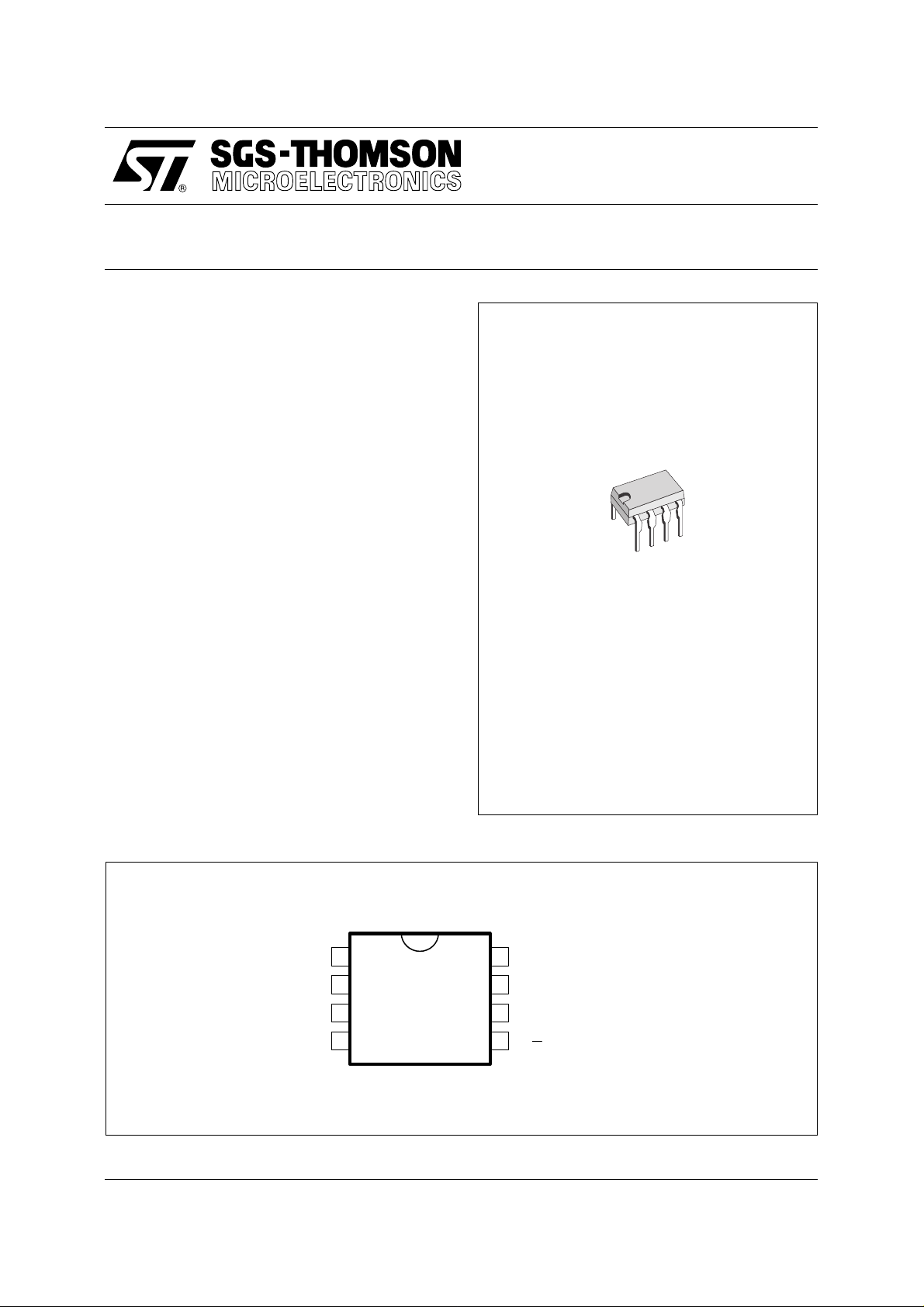
TEA5170
DIP8
(Plastic Package)
ORDER CODE : TEA5170
PIN CONNECTIONS
SOFT-START CAPACITOR
SUPPLY VOLTAGE
POWER OUTPUT
GROUND
September 1993
CSF
V
CC
P
GND
1
2
3
4
8
7
6
5
OSCILLATOR RESISTOR
RT
OSCILLATOR CAPACITOR
CT
VOLTAGE ERROR AMPLIFIER OUTPUT
E
OUTOUT
VOLTAGE ERROR AMPLIFIER
E
INVERTING INPUT
5170-01.EPS
1/9
Page 2
TEA5170
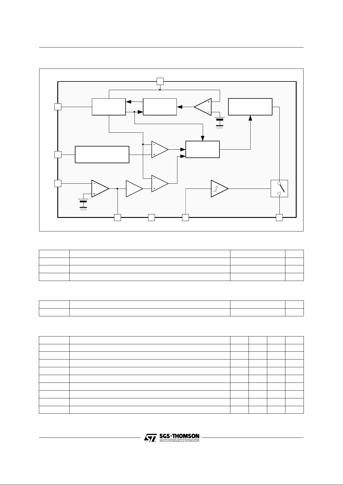
BLOCK DIAG RAM
7
Ct
OSCILLATOR
Rt
8
LOGIC
(SYNCHRO)
Comparator
POWER OUTPUT
STAGE
2.7V
Csf
1
SOF T ST ART AN D
DUTY CYCLE LIMITING
PWM
LOGIC
Error Amplifier
E-
5
x -1
2V
PWM
VMonitor
CC
642 3
Eout GND
V
CC
P
out
ABSOLUTE MAXIMUM RATINGS
Symbol Parameter Value Unit
V
CC
T
T
stg
Supply Voltage 15 V
Operating Junction Temperature 150 °C
j
Storage Temperature Range – 40, + 150 °C
THERMAL D ATA
Symbol Parameter Value Unit
R
th (j-a)
Junction-ambient Thermal Resistance 90 °C/W
5170-02.EPS
5170-01.TBL
5170-02.TBL
RECOMMAN DED OPE R ATING CO NDIT IO NS
Symbol Parameter Min. Typ. Max. Unit
V
CC
RT Timing Resistor 47 180 kΩ
CT Timing Capacitor 0.12 1.8 nF
Fosc Oscillator Frequency 12 250 kHz
Fsy Synchro Frequency 12 64 kHz
T
amb
VRT Voltage on Pin RT (8) 7 Volt
VCT Current on Pin CT (1) 100 µA
I
SOURCE
2/9
Power Supply Voltage 5 14 V
Operating Ambient Temperature – 20 70 °C
Output Current 30 60 mA
5170-03.TBL
Page 3

TEA5170
ELECTRICAL CHARACTERISTICS (TA = 25oC, VCC = 12V, unless otherwise specified)
Symbol Parameter Test Conditions Min. Typ. Max. Unit
OSCILLATOR
TA Free Period RT = 100kΩ ± 0%
CT = 1.2nF ± 0%, Vcc = 12V
TB RT = 100kΩ ± 0%
CT = 560pF ± 0%, Vcc = 12V
∆F
OSC
(T)
∆F
OSC
(VCC)
Frequency drift due to ambient
temperature variation from 0oC to 70oC
F
(70oC) − F
OSC
70
o
C x F
OSC
OSC
(25oC)
Frequency drift due to VCC variation
from 5V to 12V
(12V) − F
F
OSC
7V x F
OSC
OSC
(12V)
ERROR VOLTAGE AMPLIFIER (V
(0oC)
(5V)
CC
= 12V)
RT = 100kΩ ± 0%
CT = 1.2nF ± 0%, Vcc = 12V
RT = 100kΩ ± 0%
CT = 1.2nF ± 0%
Ibias Input Bias Current Ein = 2V 0 0.2 1 µA
Gvol Voltage Gain 80 dB
GB Gain Bandwidth 2 MHz
Slew Rate 2V/µs
INTERNAL VOLTAGE REFERENCE
V
REF
∆V
(VCC) Line Regulation
REF
∆V
REF
T
ON MIN
T
ONMIN A
T
ONMIN B
Voltage Reference Using the voltage error
amplifier as a follower
(T) V
drift with temperature
REF
V
(70oC) − V
REF
70
o
C
V
REF
REF
(12V) − V
7V
(0oC)
REF
(5V)
VCC = 5V to 12V – 3 0.4 3 mV/V
TA = 0°C to 70°C 0.2 mV/°
Minimum Duty Cycle Ct = 1.2nF ± 0%
Rt = 100kΩ ± 0%
Minimum Duty Cycle Ct = 560pf ± 0%
Rt = 100kΩ ± 0%
POWER OUTPUT STAGE
V
POUTH
V
POUTL
I
SINK
I
SOURCE
Output High Level I
Output Low Level I
Sink Current V
Source Current V
= 1mA 6.3 6.9 7.5 V
load
= – 1mA 0.5 0.8 1.1 V
load
= 3V 30 60 190 mA
POUT
= 3V 30 110 190 mA
POUT
SYNCHRONISATION
F
trig Max
V
trig
T
trigp
Wtrig +
Wtrig –
Maximum Synchro Frequency 64 kHz
Synchro Triggering Threshold 2.7 3 V
Synchro Triggering Pulse Width at VRT = 2.7Volt (fig 5) 800 nS
T
− T
trig+
O
Positive Triggering Window
Negative Triggering Window
T
O
T
− T
O
T
O
CT = 1.2nF ± 0%
RT = 100kΩ ± 0%
−
trig
CT = 1.2nF ± 0%
RT = 100kΩ ± 0%
SOFT START
I
csf
Donmax Maximum Duty Cycle V
*Csf Load Current V
= 1V 2.5 3.7 6 µA
csf
> 2.5V, VCC = 12V
cs
CT = 1.2nf ± 0%
RT = 100kΩ ± 0%
*Csf is a high impedance capacitor
60.40 65.60 70.80 µS
29.18 31.70 34.22 µS
0.01 %/°C
0.07 %/V
1.9 2 2.1 V
1.77 2.53 3.29 µs
1.04 1.49 1.94 µs
25 35 40 %
92942%
60 78 95 %
5170-04.TBL
3/9
Page 4

TEA5170
ELECTRICAL CHARACTERISTICS (TA = 25oC, VCC = 12V, unless otherwise specified) (continued)
Symbol Parameter Test Conditions Min. Typ. Max. Unit
MONITOR
V
CC
V
START
V
HYST
V
STOP
TOTAL DEVICE
I
CC
Turn-on Threshold 3.60 4 4.40 V
Hysteresis Voltage 100 mV
Turn-off Threshold 3.50 V
Supply Current RT = 100kΩ ± 0%, CT = 1.2nf ± 0%
No Load on Pin 3, VCC = 12V
71225mA
5170-05.TBL
GENERAL DES CRI PTI O N
The TEA5170 takes place in the secondary part of
an isolated off-line SMPS. During normal mode
operation, it sends pulses to the slave circuit located in the primary si de (TEA 2164, T EA2260/61)
through a pulse transformer to achieve a very
precisely regulated voltage by duty cycle control.
The main blocs of the circuit are :
- an error voltage amplifier
- an RC oscillator
- an output stage
-a V
monitor
CC
- a voltage reference bloc
- a pulse width modulator
- two logic blocs
- a soft start and Duty cycle limiting bloc
PRINCIPL E OF OPER ATION
The TEA5170 sends pulses continuously to the
slave circuit in order to insure a proper behaviour
of the primary side.
- According to this, the output duty cycle is vary ing
between D
ON (min.)
(0.05) and D
ON (max.)
(0.75) :
then even in case of open load, pulses are still
sent to the slave circuit.
Figure 1 : Basic Concept
ASYNCHRONIZED MODE (Figure 2)
The regulated voltage image is compared to 2V
vol-tage reference. The error voltage amplifier output and the RC oscillator voltage ramp are applied
to the internal Pulse Width Modulator Inputs.
The PWM logic Output is connected to a logic bloc
which behaves like a RS latch, sets by the PWM
output and resets when Ct downloading occurs.
Finally, the push-pull output bloc delivers square
wave signal whom output leading edge occurs
during Ct uploading time, and output trailing edge
at Ct downloading time end. The duty cycle is
limited to 75% of oscillator period as maximum
value and to Ct downloading time/oscillator period
as minimum value (Figure 2).
Figure 2
V2
V
t
OSCILLATOR RAMP
POWER OUTPUT
max.
V1
4/9
SLAVE
CIRCUIT
MASTER-SLAVE ARCHITECTURE
MASTER
CIRCUIT
PWM
T1
T
on max.
T2 =T
SYNCHRONIZED MODE (see Figure 3)
The TEA5170 will enter the Synchronized Mode
when it receives one pulse through Rt during Ct
discharge.
At that time Ct charging current will be multiplied
by 0.75 and period will increase up to To x 1.26.
A pulse occur ing during the s ync hro window , commands the Ct downloading. If none, the TEA5170
will return to normal mode at the end of the period.
5170-03.EPS
on min.
5170-04.EPS
Page 5

Figure 3
TEA5170
UNSYNCHRONIZED
MODE
Vct
Vtsy
Vrt
Wtrig- Wtrig+
SYNCHRONIZED MODE
Remark : In case of an application between
TEA5170 and TEA2164, t o optimize th e
synchronization windows of these
circuits, the following relations have to
be used : T
T
SYNC
=
m
1.06
Te =
T
m
1.223
with Te : Free period of the TEA2164
oscillator, and T
: Free period of the
m
TEA5170 oscillator .
UNSYNCHRONIZED
MODE
Figure 4 : Triggering Schematic
7
Ct
1kΩ
5170-05.EPS
V
CC
from logic
BLOCK DESCRIPTION
The error voltage am plifier invert ing-input and output are accessible to use different feed-back network and allowing parasitic filtering network. The
non-inverting input is internaly connected to 2V
reference voltage.
The RC oscillator is designed to work at high
frequency (up to 250kHz). R
charging current Io = 2/R
The capacitor C
during T1 =
an integrated resistor R
is loaded from V1 ≈ 1V to V2 = 2V
T
C
T RT
and then down loaded through
1.985
2
sets the capacitor
T
.
T
≈ 1kΩ during T2 = 1300 C
The ramp is used to limit the duty cycle. Then the
maximum duty cycle is
DONMAX =
The output level is V
1
T1 +
(0.73 T1 + T2)
T2
independant when VCC is
CC
over 8V.
The V
V
CC
monitoring switches the circuit on when
CC
is over 4V and s witches it of f when under 3.8V.
This function insures a proper starting procedure
(made by the primary side circuit).
SYNCHRONIZATION
(see Figures 4 and 5)
Network
Figure 5 : Typical W avef orms
T
Vct
Vrt
2.7V
2V
2.7V
8
2.7V
+
towards logic
5170-06.EPS
Rt
1V
T
trigP
5170-07.EPS
5/9
Page 6

TEA5170
STARTING
When VCC is under 4V, output pulses are not
allowed and the slave circuit keeps its own mode.
When V
is going over 4V, output pulses are sent
CC
via the pulse transformer (or an optical device) to
the slave circuit which is synchronizing and entering the slaved mode. Output pulses can be shut
down only if V
goes below 3.8 Volt.
CC
Figure 6 : Soft-Start Sequence
V (V)
CC
12
4
V (V)
CSF
3.2
2
SOFT START
Using Csf, it is possible to make a soft start sequence. When V
on Csf equals 0V. When V
grows from 0V to 4V, voltage
CC
is higher than 4V, Csf
CC
is loaded by a 3.7µA current, then TonMAX (Vcsf)
will vary linearly f rom Tonmin to Tonmax according
to Csfst bias.
When V
will go low (3.8 Volt threshold), Csf will
CC
be downloaded by an internal transistor.
t
t
Duty cycle
D
on max.
D
on min.
POWER OU TPUT STAGE
Figure 7 : Electrical Schematic
1mA
from logic
V
1mA
CC
maximum
minimum
Pout
3
t
5170-08.EPS
6/9
5170-09.EPS
Page 7

Figure 8
135V
TEA5170
Sync.
Input
P1
47kΩ
100µF
(250V)
BY218-600
G4466-01
313
120kΩ
15V
470µF
BA157
20
2.2kΩ
10V
10kΩ
(25V)
1000µF
(25V)
BY218-100
19
14
6
9
Stand-by
Control
Ω
75k
3.3
nF
BC547C
20V
470µF
(40V)
BY318-100
22
21
717
TEA5170
16V
3781
220Ω
(8W)
BA159
2465
10µF
BUV56A
47nF
1.2nF2%
4.7nF
1kV
150pF
1N4148
Ω
270
Ω
100k
6.8kΩ
1%
Pulse
Transformer
Ω
100
4 x BY254
BA157
(3W)
Ω
220µF
4.7
(2W)
44kΩ
220µF
(250V)
68kΩ
20%110
AC
V
P2
1nF
25V
18Ω BZX85C-3V0
2.2µF47µF
6.8Ω
(3W)
141
15
22kΩ
4 5 12 13 16
9
10
100nF
2
11
F
µ
4.7
3
TEA2164
1.2nF2%
8
76
100Ω
0.18Ω (1W)
1N4148
330
Ω
1kΩ
16V
1nF
: 90W
OUT
f : 16kHz
1%
110kΩ
P
5170-10.EPS
7/9
Page 8

TEA5170
Figure 9
135V
0.8A
Sync.
Input
Ω
12V
Ω
2.2k
120k
7.5V
1A
Stand-by
Control
Ω
Ω
10k
75k
5
6
4
1.2
nF
0.5A
F
µ
470
(25V)
BC547C
25V
F
µ
1000
(25V)
F
µ
1000
(40V)
2
F
µ
10
16V
1
8
7
TEA5170
560
3
150pF
6.8kΩ100kΩ
47nF
1N4148
pF
Ω
P1
47k
(250V)
100µF
270Ω1kΩ
BY218-600
G4576-02
4 x 1N4007
AC
V
170
PLR811
BY218-100
13
20
19
14717922
BY218-100
21
220Ω(16W)
3
6
2.7nF
BY299
1kV
SGSF344
100
pF
BA157
1N4148
Ω
39
(3W)
18kΩ
150µF
(385V)
Ω
4.7k
AC
V
270
P2
F
µ
330
2.2Ω (0.5W)
25V
6.8Ω
(1W)
22kΩ
1
BZX85C -3V0
18Ω
2.2µF47µF
16 15
314
(16V)
2.2µF
1nF
12 13
5
8
9
TEA2164
4
1kΩ
1kΩ
Ω
22k
6
7
3.3nF
220nF
220nF
2
1nF
11 10
Ω
56kΩ
100Ω
(1W)
Ω
0.135
330Ω
150k
: 140W
OUT
f : 32kHz
P
BC547C
8/9
1MΩ
5170-11.EPS
Page 9

PACKAGE MECHANICAL DATA
8 PINS - PLASTIC DIP
b
Z
D
e3
TEA5170
e4
I
A
L
a1
B
B1
e
E
Z
b1
8
5
F
14
Dimensions
Min. Typ. Max. Min. Typ. Max.
Millimeters Inches
A 3.32 0.131
a1 0.51 0.020
B 1.15 1.65 0.045 0.065
b 0.356 0.55 0.014 0.022
b1 0.204 0.304 0.008 0.012
D 10.92 0.430
E 7.95 9.75 0.313 0.384
e 2.54 0.100
e3 7.62 0.300
e4 7.62 0.300
F 6.6 0260
i 5.08 0.2 00
L 3.18 3.81 0.125 0.150
Z 1.52 0.060
Information furnished i s believed to be accurate and rel iabl e. However, S GS-THOMSON Microel ectroni cs assumes no responsibil ity
for the consequences of use of such information nor for any infringement of patents or other rights of third parties which may result
from its use. No licence is granted by implication or otherwise under any patent or patent rights of SGS-THOMSON Microelectronics.
Specifications mentioned in this publication are subject to change without notice. This publication supersedes and replaces all
information previously supplied. SGS-THOMSON Microelectronics products are not authorized for use as critical components in life
support devices or systems without express written approval of SGS-THOMSON Microelectronics.
PM-DIP8.EPS
DIP8.TBL
© 1994 SGS-THOMSON Microelectronics - All Rights Reserved
2
Purchase of I
2
C Patent. Rights to use these components in a I2C system, is granted provided that the system conforms to
I
Australia - Brazil - China - France - Germany - Hong Kong - Italy - Japan - Korea - Malaysia - Malta - Morocco
The Netherlands - Singapore - Spain - Sweden - Switzerland - Taiwan - Thailand - United Kingdom - U.S.A.
C Components of SGS-THOMSON Microelectronics, conveys a license under the Philips
2
C Standard Specifications as defined by Philips.
the I
SGS-THOMSON Microelectronics GROUP OF COMPANIES
9/9
 Loading...