

Page 1
RGB HIGH VOLTAGE VIDEO AMPLIFIER
.
BANDWIDTH : 10MHzTYPICAL
.
RISE ANDFALL TIME: 50nsTYPICAL
.
CRT CATHODES CURRENT OUTPUTS FOR
PARALLEL OR SEQUENTIAL CUT-OFF OR
DRIVEADJUSTMENT
.
FLASHOVERPROTECTION
.
POWER DISSIPATION : 3.5W
.
ESD PROTECTED
TEA5101B
PRELIMINARY DATA
DESCRIPTION
The TEA5101B includes three video amplifiers
desi-gnedwith a high voltageDMOS/bipolar technology. It drives directly the three CRT cathodes.
The deviceis protected againstflashovers. Due to
its three cathode current outputs, the TEA5101B
canbe usedwithboth parallel andsequentialsamplingapplications.
PINCONNECTIONS (topview)
15
14
13
12
11
10
9
8
7
6
5
4
3
2
1
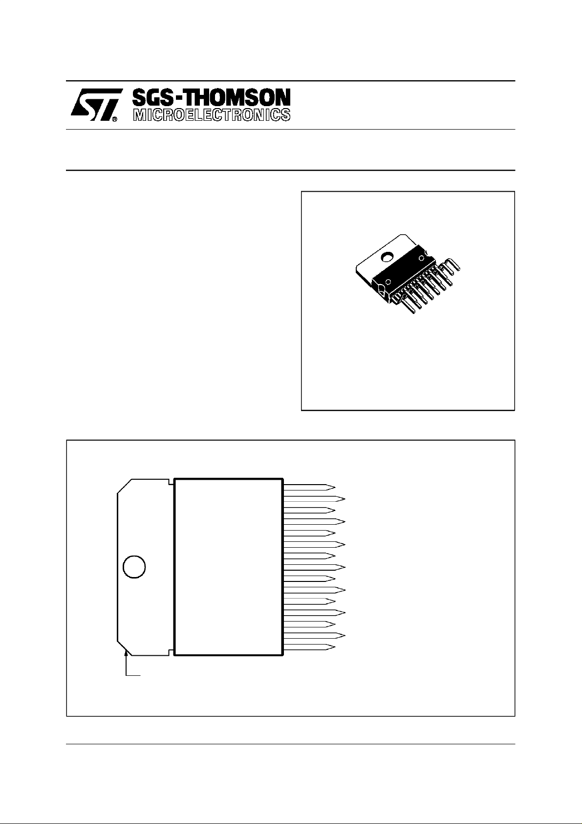
MULTIWATT 15
(Plastic Package)
ORDER CODE : TEA5101B
BLUE FEEDBACK
BLUE CATHODE CURRENT
BLUE OUTPUT
GREEN FEEDBACK
GREEN CATHODE CURRENT
GREEN OUTPUT
RED FEEDBACK
GROUND
RED OUTPUT
RED CATHODE CURRENT
V HIGH VOLTAGE
DD
RED INPUT
GREEN INPUT
V LOW VOLTAGE
CC
BLUE INPUT
Tab connected to Pin 8
May 1996
This isadvance informationon a new product now in development or undergoing evaluation. Detailsare subject to changewithout notice.
5101B-01.EPS
1/6
Page 2
TEA5101B
PIN FUNCTION
N° Function Description
1 Blue Input Input of the ”blue” amplifier. It is a virtualground with 3.8V bias voltage,
2V
CC
3 Green Input See Pin 1.
4 Red Input See Pin 1.
5V
DD
6 Red Cathode Current Provides the video processor with a copyof the DC current flowing into the red
7 Red Output Output driving the red cathode. Pin7 is internallyprotected against CRT arc
8 Ground Also connected to the heatsink.
9 Red Feedback Output driving the feedback resistor network for the redamplifier.
10 Green Output See Pin 7.
11 Green Cathode Current See Pin 6.
12 Green Feedback See Pin 9.
13 Blue Output See Pin 7.
14 Blue Cathode Current See Pin 6.
15 Blue Feedback See Pin 9.
15 microamperes input bias current with14kΩ input resistance.
Low voltage power supply, typically 12V.
Highvoltage power supply, typically 200V.
cathode, for automatic cut-off or gainadjustment. If this control is not used,
Pin 6 must be grounded.
discharges by a diode limiting the output voltage to V
DD
.
5101B-01.TBL
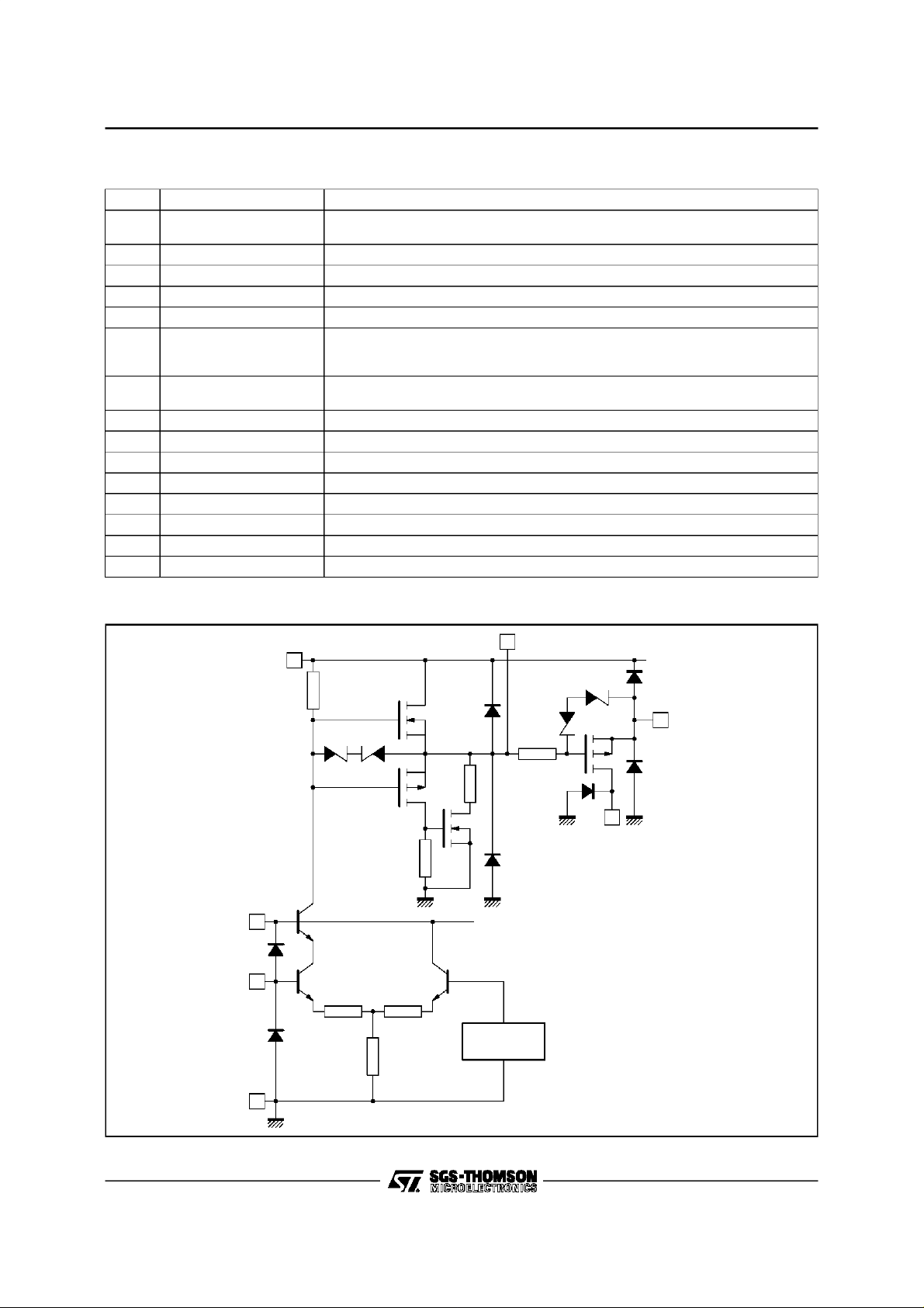
BLOCK DIAGRAM OF EACH CHANNEL
DD
5
40kΩ
2
1
(3, 4)
35Ω 35Ω
350
1kΩ
Ω
0.8kΩ
(12, 9)15V
20k
REFERENCE
VOLTAGE
13
Ω
(11, 6)
(10, 7)
14
2/6
GND
8
5101B-02.EPS
Page 3

TEA5101B
ABSOLUTE MAXIMUM RATINGS
Symbol Parameter Value Unit
V
V
T
T
THERMALDATA
Symbol Parameter Value Unit
R
th
R
th
ELECTRICAL CHARACTERISTICS
T
amb
Symbol Parameter Min. Typ. Max. Unit
V
V
I
I
V
R
BW Bandwidth (– 3db) (measured on CRT cathodes)
T
R-TF
G
V
I
R
SupplyHigh Voltage Pin 5 250 V
DD
SupplyLow Voltage Pin 2 20 V
CC
Output Current
I
to V
O
I
O
DD
to Ground
Output Current
to V
I
F
I
F
I
j
T
j
oper
stg
DD
to Ground
InputCurrent Pins 1 - 3 -4 60 mA
JunctionTemperature 150 °C
Operating Ambient Temperature 0 to 70 °C
Storage Temperature – 55 to + 150 °C
Pins 7 - 10 - 13
Protected
8mA
Pins 9 - 12 - 15
45
45
(j-c) Maximum Junction Case Thermal Resistance Max. 3 °C/W
(j-a) TypicalJunction Ambient Thermal Resistance Typ. 35 °C/W
=25oC;VCC=12V ; VDD=220V ; AV= 55 (unlessotherwise specified)
High SupplyVoltage Pin 5 200 220 V
DD
Low Supply Voltage Pin 2 10 12 15 V
CC
High VoltageSupply Internal DC Current (V
DD
(without the current due to the feedback network )
Low Voltage Supply Internal DC Current 38 55 mA
CC
Output Saturation Voltage (High level)
sath
ON
=–10µA
I
O
Output Mos Transistor (Low level)
R
ON@IO
(C
=3mA
: 10pF –R Protect = 1kΩ –V
LOAD
:50V
∆ V
∆ V
out
out
: 100 V
PP
PP
out
Rise Time andFall Time : measured between 10% and90% of output
pulse(C
∆ V
Open LoopGain 47 53 dB
O
: 10 pF – R Protect = 1 kΩ –V
LOAD
: 100 V
out
PP
Open LoopGain Difference between 2 channels -1.5 0 +1.5 dB
Open LoopGain Temperature Coefficient 0 dB/
P InternalPower Dissipation (see calculation below) 3.5 W
Internal Voltage Reference Pins 1-3-4 3.55 3.85 4.15 V
REF
Internal Reference Voltage Difference Between 2 Channels 250 mV
VoltageReference Temperature Coefficient 0 mV/°C
InputBias Current (V
IB
InputResistance 14 kΩ
I
: 100 V) Pins 1-3-4 15 µA
out
out
= 100V)
out
100V)
= 100 V)
Pin 5 9.5 15 mA
Pins 7-10-13 3 10 V
Pins 7-10-13 1.7 kΩ
10
8
50 ns
mA
mA
MHz
MHz
5101B-02.TBL
5101B-03.TBL
o
C
5101B-04.TBL
3/6
Page 4

TEA5101B
TYPICALAPPLICATION
The TEA5101Bconsists of three independentamplifiers. Each of themincludes :
- Adifferential amplifier, the gain of which is fixed
by external feedbackresistors,
12V
V
CC
10
µF
25
39kΩ
- Avoltage reference,
- A PMOS transistor providing a copy of the cathode current,
- Aprotectiondiode againstCRT arcdischarges.
200V
V
DD
4.7µF
V
DD
9
1nF
* optional
10pF*
1.8kΩ
220
Ω
4
V
REF
V
DD
3
V
DD
7
1kΩ
6
12
220Ω
10
11
15
CATHODE1
4/6
1
TEA5101B
8
13
14
CUT-OFF
SAMPLING
5101B-03.EPS
Page 5

APPLICATION INFORMATION
PC BOARDLAYOUT
The best performances of the high voltage video
amplifierwillbe obtainedonlywith a carefullydesigned PC board. Outputto input capacitancesare
of particularimportance.
For a single amplifier, the input-output capacitance, in parallel with therelatively high feedback
resis-tance,createsa poleintheclosed-looptransfer function. A low parasitic capacitance (0.3pF)
feedbackresistor andHFisolated printedwiresare
necessary.Furthermore, capacitive couplingfrom
the output of an amplifier toward the input of another one mayinduce excessive crosstalk.
POWERDISSIPATION
The powerdissipationconsists of astatic part and
a dynamic part. The static dissipation varies with
the output voltage.With V
typ(3.5Wmax) at V
= 100V,1.5W typ at 150V
OUT
= 200V, P
DD
stat
= 2.6W
and 3W typ at 50V (with R feedback= 39kΩ).
TEA5101B
firstvalue (100V) will be thereference.
V
OUT
The dynamic dissipation depends on the signal
spectrumand the load capacitance.
- Dynamicpower witha typicalpicturewith150 V
modulationis typically 1W.
- Forasinewave,dynamicdissipation peramplifier
=FxClxV
is P
d
oppxVdd
The load capacitance C
x 0.8.
includesCRT andboard
L
capacitance (10pF), and amplifier output capacitance (8pF) : total C
5MHZ,50 V
sinewave anda 20pFload capaci-
pp
value is about 20pF. For a
L
tance, the maximum dynamicpower is 2.5W.
- Generally, the maximum dynamic power is
reached witha white noise (tunernoise).
- Typicalvalue is about2W.
Total dissipation is typically 3.6W (2.6W + 1W).
With a maximum static dissipation of 3.5W, total
dissipationis :
- 4.5Wwith a typical picture(UER pattern)
- 5.5Wwith white noise
pp
5/6
Page 6

TEA5101B
PACKAGE MECHANICAL DATA : 15 PINS– PLASTICMULTIWATT
Dimensions
Min. Typ. Max. Min. Typ. Max.
A 5 0.197
B 2.65 0.104
C 1.6 0.063
D 1 0.039
E 0.49 0.55 0.019 0.022
F 0.66 0.75 0.026 0.030
G 1.02 1.27 1.52 0.040 0.050 0.060
G1 17.53 17.78 18.03 0.690 0.700 0.710
H1 19.6 0.772
H2 20.2 0.795
L 21.9 22.2 22.5 0.862 0.874 0.886
L1 21.7 22.1 22.5 0.854 0.870 0.886
L2 17.65 18.1 0.695 0.713
L3 17.25 17.5 17.75 0.679 0.689 0.699
L4 10.3 10.7 10.9 0.406 0.421 0.429
L7 2.65 2.9 0.104 0.114
M 4.25 4.55 4.85 0.167 0.179 0.191
M1 4.63 5.08 5.53 0.182 0.200 0.218
S 1.9 2.6 0.075 0.102
S1 1.9 2.6 0.075 0.102
Dia. 1 3.65 3.85 0.144 0.152
Information furnishedis believedtobe accurate and reliable.However, SGS-THOMSON Microelectronicsassumes no responsibility
for the consequences of use of such information norfor anyinfringement of patents or other rights of third parties which may result
from its use. No licence is granted byimplication or otherwise underany patent or patentrights of SGS-THOMSON Microelectronics.
Specifications mentioned in this publication are subject to change without notice. This publication supersedes and replaces all
information previouslysupplied. SGS-THOMSON Microelectronics products are not authorized for use as criticalcomponents in life
support devices or systems without express written approvalof SGS-THOMSON Microelectronics.
Millimeters Inches
PM-MW15V.EPS
MW15V.TBL
6/6
1996 SGS-THOMSON Microelectronics -All RightsReserved
Purchase of I2C Components of SGS-THOMSON Microelectronics, conveys a license under the Philips
2
I
C Patent. Rights to use these components in a I2C system,is granted provided that the system conformsto
Australia - Brazil -Canada -China - France - Germany- Hong Kong - Italy -Japan - Korea - Malaysia - Malta - Morocco
The Netherlands - Singapore - Spain - Sweden - Switzerland - Taiwan - Thailand - UnitedKingdom -U.S.A.
2
the I
C Standard Specifications as defined by Philips.
SGS-THOMSON Microelectronics GROUP OF COMPANIES
 Loading...