

Page 1

RGB HIGH VOLTAGE VIDEO AMPLIFIER
.
BANDWIDTH : 10MHzTYPICAL
.
RISE ANDFALL TIME : 50nsTYPICAL
.
CRT CATHODES CURRENT OUTPUTS FOR
PARALLEL OR SEQUENTIAL CUT-OFF OR
DRIVEADJUSTMENT
.
FLASHOVERPROTECTION
.
POWER DISSIPATION : 3.5W
.
ESD PROTECTED
TEA5101A
DESCRIPTION
The TEA5101A includes three video amplifiers
desi-gnedwitha high voltageDMOS/bipolar technology. It drives directly the three CRT cathodes.
The deviceisprotectedagainstflashovers. Dueto
its three cathode current outputs, the TEA5101A
canbeused withboth paralleland sequentialsamplingapplications.
PINCONNECTIONS (topview)
15
14
13
12
11
10
9
8
7
6
5
4
3
2
1
MULTIWATT 15
(Plastic Package)
ORDER CODE : TEA5101A
BLUE FEEDBACK
BLUE CATHODE CURRENT
BLUE OUTPUT
GREEN FEEDBACK
GREEN CATHODE CURRENT
GREEN OUTPUT
RED FEEDBACK
GROUND
RED OUTPUT
RED CATHODE CURRENT
V HIGH VOLTAGE
DD
RED INPUT
GREEN INPUT
V LOW VOLTAGE
CC
BLUE INPUT
June 1993
Tab connectedto Pin 8
5101A-01.EPS
1/6
Page 2
TEA5101A
PIN FUNCTION
N° Function Description
1 Blue Input Input of the ”blue” amplifier. It is a virtual ground with 3.8V bias voltage,
2V
CC
3 Green Input See Pin 1.
4 Red Input See Pin 1.
5V
DD
6 Red Cathode Current Provides the video processor with a copy ofthe DC current flowing into the red
7 Red Output Output driving the red cathode. Pin 7 is internally protected against CRT arc
8 Ground Also connected to the heat sink.
9 Red Feedback Output driving the feedback resistor network for the red amplifier.
10 Green Output See Pin 7.
11 Green Cathode Current See Pin 6.
12 Green Feedback See Pin 9.
13 Blue Output See Pin 7.
14 Blue Cathode Current See Pin 6.
15 Blue Feedback See Pin 9.
15 microamperes input bias current with 14kΩ input resistance.
Low voltage power supply, typically 12V.
Highvoltage power supply, typically 200V.
cathode, for automatic cut-off or gain adjustment. If this control is not used, Pin 6
must be grounded.
discharges by a diode limiting the output voltage to V
DD
.
5101A-01.TBL
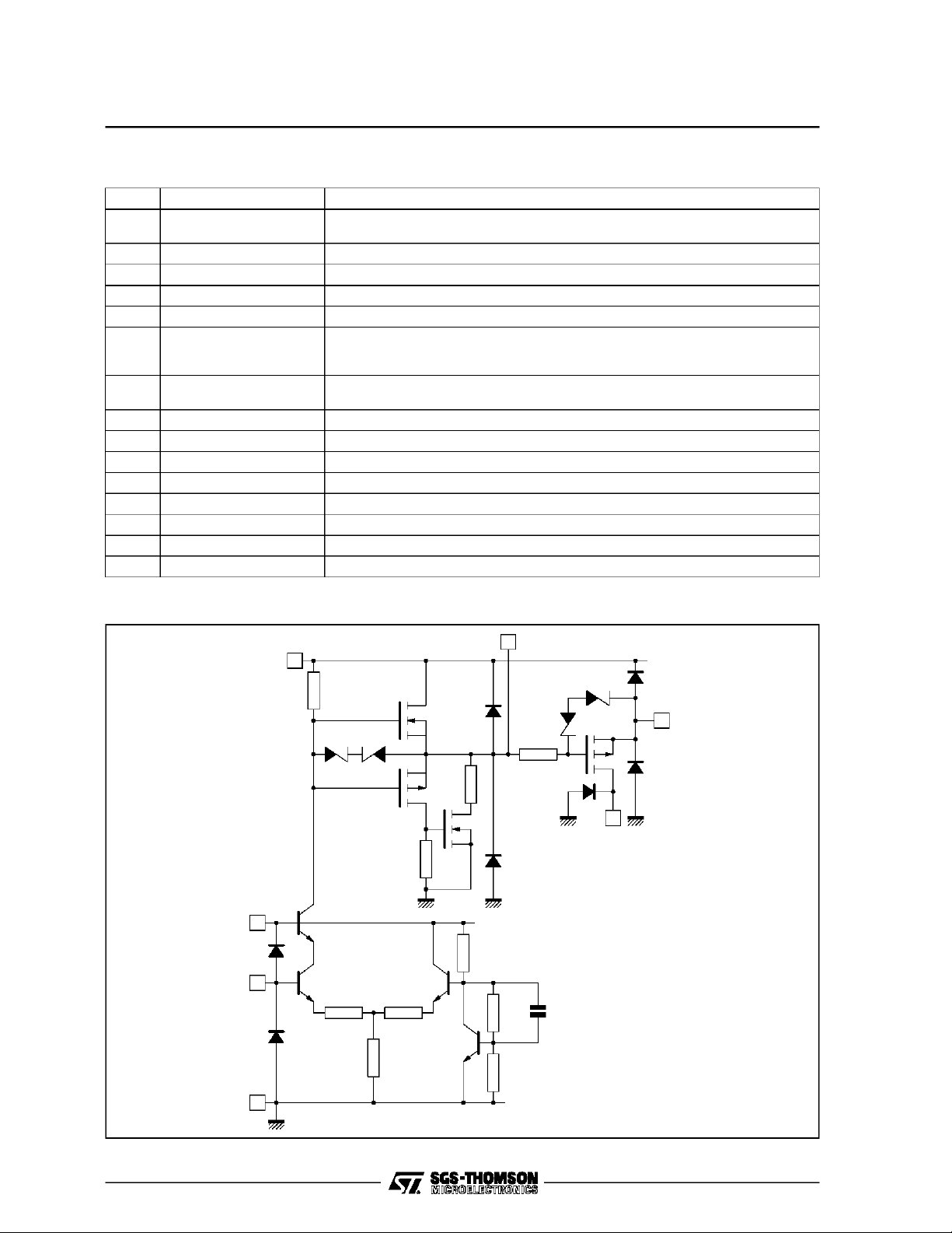
BLOCK DIAGRAM OF EACH CHANNEL
DD
5
40kΩ
2
1
(3, 4)
GND
8
35Ω 35Ω
1kΩ
350Ω
0.8k
(12, 9)15V
13
20k
Ω
Ω
(11, 6)
2.5kΩ
6kΩ
3pF
1.5kΩ
(10, 7)
14
2/6
5101A-02.EPS
Page 3

TEA5101A
ABSOLUTE MAXIMUM RATINGS
Symbol Parameter Value Unit
V
V
T
T
THERMALDATA
Symbol Parameter Value Unit
R
th
R
th
ELECTRICAL CHARACTERISTICS
T
amb
Symbol Parameter Min. Typ. Max. Unit
V
V
I
I
V
R
BW Bandwidth (– 3db) (measured on CRT cathodes)
T
R-TF
G
V
I
R
SupplyHigh Voltage Pin 5 250 V
DD
SupplyLow Voltage Pin 2 35 V
CC
Output Current
I
to V
O
I
O
DD
to Ground
Output Current
to V
I
F
I
F
I
j
T
j
oper
stg
DD
to Ground
InputCurrent Pins 1 - 3 - 4 60 mA
JunctionTemperature 150 °C
Operating Ambient Temperature 0 to 70 °C
Storage Temperature – 55 to + 150 °C
Pins 7 - 10 - 13
Protected
8mA
Pins 9 - 12 - 15
45
45
(j-c) Maximum Junction Case Thermal Resistance Max. 3 °C/W
(j-a) TypicalJunction Ambient Thermal Resistance Typ. 35 °C/W
=25oC;VCC=12V ; VDD=200V; AV=50(unlessotherwise specified)
High Supply Voltage Pin 5 200 220 V
DD
Low Supply Voltage Pin 2 10 12 15 V
CC
High Voltage Supply Internal DC Current (V
DD
(without the current due to the feedback network )
Low Voltage Supply DC Current Pin 2 19 33 47 mA
CC
Output Saturation Voltage (High level)
sath
ON
=–10µA
I
O
Output Mos Transistor (Low level)
R
ON@IO
(C
=3mA
: 10pF – R Protect = 1kΩ –V
LOAD
:50V
∆ V
∆ V
out
out
: 100 V
PP
PP
out
Rise Time and Fall Time : measured between10% and90% of output
pulse(C
∆ V
Open Loop Gain 47 50 dB
O
: 10 pF – R Protect = 1 kΩ –V
LOAD
: 100 V
out
PP
P Internal Power Dissipation (see calculation below) 3.5 W
Internal Voltage Reference Pins 1-3-4 3.55 3.8 4.05 V
REF
Internal Reference Voltage Difference Between 2 Channels 5 %
VoltageReference Temperature Coefficient – 5 mV/°C
InputBias Current (V
IB
InputResistance 14 kΩ
I
: 100 V) Pins 1-3-4 15 µA
out
out
= 100V)
out
100V)
= 100 V)
Pin 5 8 12 mA
Pins 7-10-13 3 10 V
Pins 7-10-13 1.7 kΩ
10
8
50 ns
mA
mA
5101A-02.TBL
5101A-03.TBL
MHz
MHz
5101A-04.TBL
3/6
Page 4

TEA5101A
TYPICALAPPLICATION
The TEA5101Aconsists of threeindependentamplifiers. Eachof themincludes:
- A differential amplifier, the gain of which is fixed
by external feedback resistors,
12V
V
CC
10µF
25
39kΩ
10pF*
- A voltage reference,
- A PMOS transistor providing a copy of the cathode current,
- A protectiondiode against CRTarcdischarges.
200V
V
DD
4.7µF
9
V
DD
1nF
220Ω
* optional
1.8kΩ
4
V
REF
3
1
TEA5101A
8
7
1kΩ
6
12
V
DD
220Ω
10
11
15
V
DD
13
14
CATHODE 1
CUT-OFF
SAMPLING
4/6
5101A-03.EPS
Page 5

APPLICATION INFORMATION
PC BOARD LAYOUT
The best performances of the high voltage video
amplifierwill be obtained onlywith a carefullydesigned PC board. Output to input capacitancesare
of particularimportance.
For a single amplifier, the input-output capacitance, in parallel with the relatively high feedback
resis-tance,createsa poleintheclosed-looptransfer function. A low parasitic capacitance (0.3pF)
feedbackresistorandHFisolated printedwires are
necessary.Further more, capacitive couplingfrom
the output of an amplifier toward the input of another one may induce excessivecrosstalk.
POWERDISSIPATION
The powerdissipationconsists of a staticpart and
a dynamic part. The static dissipation varies with
the output voltage. With V
typ(3.5Wmax) at V
= 100V,1.5W typ at 150V
OUT
= 200V,P
DD
stat
= 2.6W
and 3W typ at 50V(with R feedback= 39kΩ).
TEA5101A
firstvalue(100V)will be the reference.
V
OUT
The dynamic dissipation depends on the signal
spectrumand theload capacitance.
- Dynamicpowerwithatypicalpicturewith150V
modulationis typically1W.
- For asinewave,dynamicdissipationperamplifier
=FxClxV
is P
d
oppxVdd
The load capacitance C
x 0.8.
includes CRTand board
L
capacitance (10pF), and amplifier output capacitance (8pF) : total C
5MHZ,50 V
sinewave and a 20pFload capaci-
pp
value is about 20pF. For a
L
tance, the maximum dynamicpoweris 2.5W.
- Generally, the maximum dynamic power is
reached with a white noise (tunernoise).
- Typical valueis about 2W.
Total dissipation is typically 3.6W (2.6W + 1W).
With a maximum static dissipation of 3.5W, total
dissipationis :
- 4.5W with a typical picture(UER pattern)
- 5.5W with white noise
pp
5/6
Page 6

TEA5101A
PACKAGE MECHANICAL DATA : 15 PINS– PLASTICMULTIWATT
Dimensions
Min. Typ. Max. Min. Typ. Max.
A 5 0.197
B 2.65 0.104
C 1.6 0.063
D 1 0.039
E 0.49 0.55 0.019 0.022
F 0.66 0.75 0.026 0.030
G 1.14 1.27 1.4 0.045 0.050 0.055
G1 17.57 17.78 17.91 0.692 0.700 0.705
H1 19.6 0.772
H2 20.2 0.795
L 22.1 22.6 0.870 0.890
L1 22 22.5 0.866 0.886
L2 17.65 18.1 0.695 0.713
L3 17.25 17.5 17.75 0.679 0.689 0.699
L4 10.3 10.7 10.9 0.406 0.421 0.429
L7 2.65 2.9 0.104 0.114
M 4.2 4.3 4.6 0.165 0.169 0.181
M1 4.5 5.08 5.3 0.177 0.200 0.209
S 1.9 2.6 0.075 0.102
S1 1.9 2.6 0.075 0.102
Dia. 1 3.65 3.85 0.144 0.152
Information furnishedis believed to be accurateand reliable.However, SGS-THOMSON Microelectronics assumes noresponsibility
for the consequences of useof suchinformation norfor anyinfringement of patents or otherrights ofthird partieswhich may result
from itsuse. Nolicence isgranted byimplicationor otherwiseunder any patent or patent rights of SGS-THOMSON Microelectronics.
Specifications mentioned in this publication are subject to change without notice. This publication supersedes and replaces all
information previouslysupplied. SGS-THOMSONMicroelectronics products are not authorized for use as criticalcomponents inlife
support devices or systems without express written approval of SGS-THOMSON Microelectronics.
Millimeters Inches
PMMUL15V.EPS
MUL15V.TBL
6/6
1994 SGS-THOMSON Microelectronics -All Rights Reserved
Purchase of I2C Components of SGS-THOMSON Microelectronics,conveys a license under the Philips
2
I
C Patent. Rights to use these components ina I2C system, isgranted provided that the system conformsto
Australia - Brazil- China - France- Germany - Hong Kong - Italy- Japan - Korea -Malaysia - Malta - Morocco
The Netherlands -Singapore - Spain - Sweden - Switzerland- Taiwan - Thailand - United Kingdom -U.S.A.
2
the I
C Standard Specifications as defined by Philips.
SGS-THOMSON Microelectronics GROUP OFCOMPANIES
 Loading...