

Page 1
.
DIGITAL CONTROL OF BRIGHTNESS,
SATURATION AND CONTRAST ON TV SIGNALS AND R, G, B INTERNAL OR EXTERNALSOURCES
.
BUS DRIVE OF SWITCHINGFUNCTIONS
.
DEMATRIXING OF R, G, B SIGNALS FROM
Y, R-Y, B-Y,TV MODE INPUTS
.
MATRIXING OF R, G, B SOURCES INTO
Y, R-Y, B-Y SIGNALS
.
AUTOMATIC DRIVE AND CUT-OFF CONTROLS BY DIGITAL PROCESSING DURING
FRAMERETRACE
.
PEAK ANDAVERAGEBEAM CURRENT LIMITATION
.
ON-CHIP SWITCHING FOR R, G, B INPUT
SELECTION
.
ON-CHIP INSERTION OF INTERNAL OR EXTERNAL R, G, B SOURCES
TEA5040S
WIDE BAND VIDEO PROCESSOR
DESCRIPTION
The TEA5040S is a serial bus-controlled videoprocessingdevice which integrates a complexarchitecturefulfilling multiplefunctions.
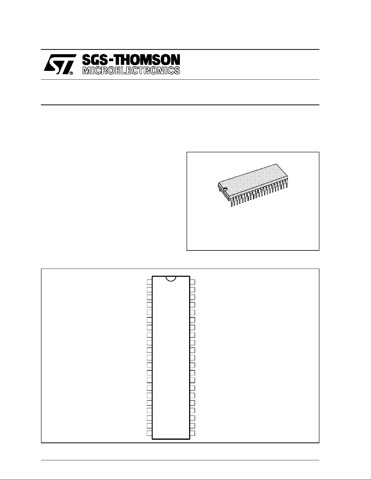
SDIP42
(Plastic Package)
ORDER CODE : TEA5040S
PINCONNECTIONS
SWITCHABLEVIDEO OUTPUT
V
1
CC
R INTERNAL INPUT
R EXTERNAL INPUT
G INTERNAL INPUT
G EXTERNAL INPUT
B INTERNALINPUT
B EXTERNAL INPUT
FB EXTERNALINPUT
FB INTERNALINPUT
B-YINPUT
R-YINPUT
Y INPUT
CLOCK
DATA
ENABLE
VOLTAGE REFERENCE
R CLAMPMEMORY
G CLAMP MEMORY
B CLAMPMEMORY
GROUND
NOT TO BE CONNECTED NOT TO BE CONNECTED
2
340
4
5
6
7
8
9
10
11
12 31
13
14
15
16
17
18
19
20
21
42
41
SYNCHRO INPUT
INTERNAL VIDEO OUTPUT
INTERNAL VIDEO INPUT
39
AVERAGE BEAM LIMIT. REF
38
EXTERNAL VIDEO INPUT
37
AVERAGEBEAMCURRENTFILTER
36
LEAKAGE CURRENT FILTER
35
CATHODE CURRENTINPUT
34
SWITCHCUT-OFFRESISTANCE
33
SUPER SANDCASTLE INPUT
32
B OUTPUT
CUT-OFFMEMORY(BCHANNEL)
30
DRIVE MEMORY (B CHANNEL)
29
G OUTPUT
28
CUT-OFFMEMORY (G CHANNEL)
27
DRIVEMEMORY (G CHANNEL)
26
R OUTPUT
25
CUT-OFFMEMORY (RCHANNEL)
24
DRIVEMEMORY (R CHANNEL)
23
22
5040S-01.EPS
April 1993
1/12
Page 2
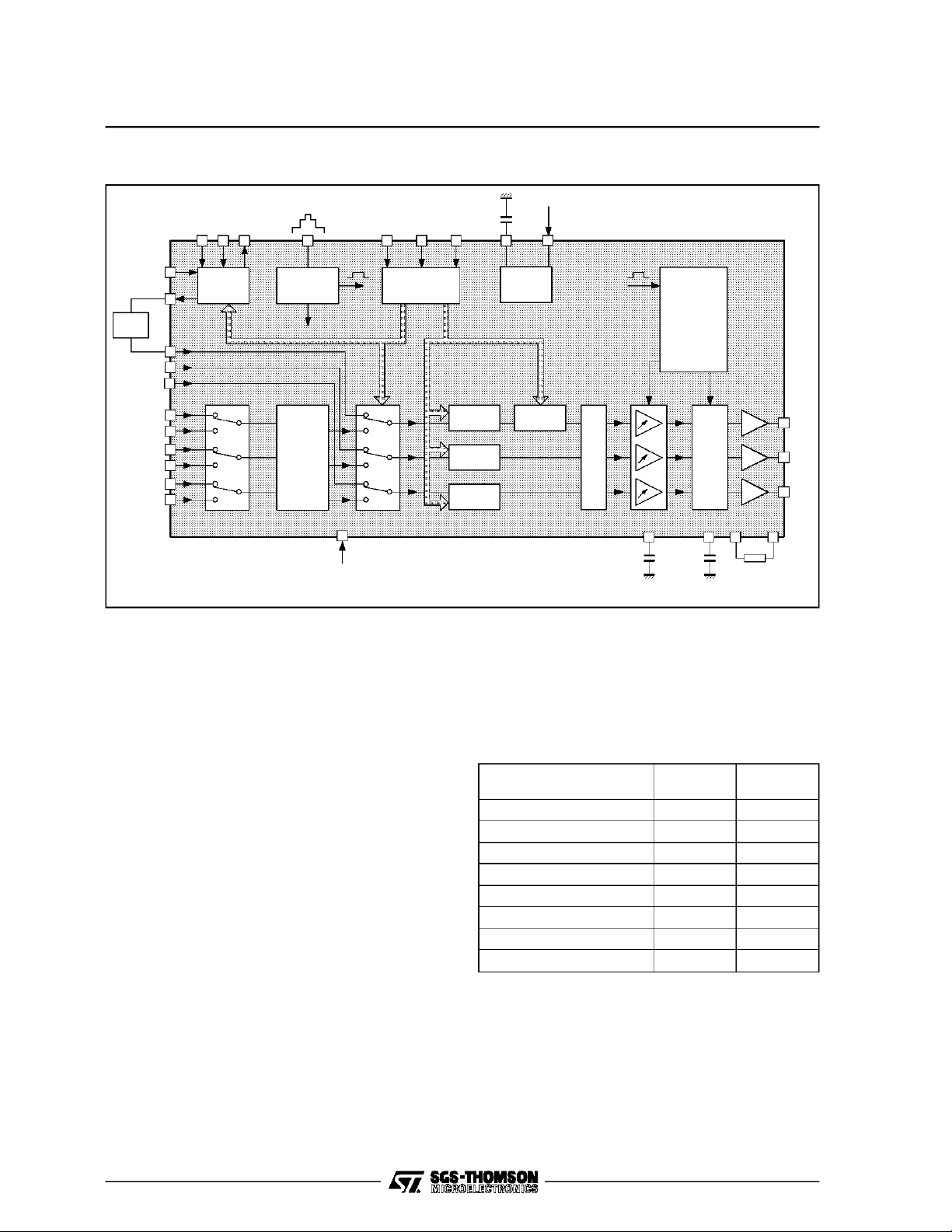
TEA5040S
BLOCK DIAGRAM
VIDEO
39
OUTEXTINT EN CLKDATA
4037
32
14 1315 36
V
REF
38
INT SYNC.
DELAY
TIME
(R - Y)
(B - Y)
41
VIDEO
SWITCH
42
Y
12
11
10
2
R
3
R’
4
G
G’
5
B
6
B’
7
R
G
B
SUPER
SAND CAS TLE
DETECTOR
Y
(R - Y)
MATRIX
(B - Y)
+ 12V
BUS
DECODER
1
GENERALDESCRIPTION
Brief Description
This integrated circuit incorporates the following
features :
- a synchro and two video inputs
- a fixed video output
- a switchablevideo output
- normalY, R-Y,B-YTV mode inputs
- doubleset of R, G, B inputs
- brightness, contrast and saturation controls as
wellon aR,G,B pictureasonanormalTVpicture
- digitalcontrol inputs by means of serialbus
- peakbeam currentlimitation
- averagebeam current limitation
- automaticdrive and cut-offcontrols
Block Diagram Description
BUSDECODER
A3 lines bus(clock,data, enable) delivered by the
BEAM
CURRENT
LIMIT
LOGIC
(R - Y)
(B - Y)
Y
MATRIX
DRIVE
MEMORIES
CONTROL
BLACK LEVEL
X3X3
CUTOFF
MEMORIES
CATHODE
CURRENTS
CONTRAST
SAT.
SAT.
BRIGHTNESS
microcontrollerof the TV-setentersthe videoprocessor integrated circuit (pins 13-14-15). A control
systemacts insuch a way that only a 9-bit word is
takenintoaccountbythevideoprocessor.Sixofthe
bits carry the data, the remaining three carry the
address of the subsystem.
Function Address
Brightness Control 0 5
Contrast Control 1 5
Colour on/off Selection 2 1
Insertion Allowed 3 1
Sync/Async Mode 4 1
Int/Ext Video Switching 5 1
B-Y Saturation Control 6 6
R-Y Saturation Control 7 6
Number of
3423 24 33
Bits
R
25
OUT
G
28
OUT
B
31
OUT
5040S-02.EPS
2/12
Page 3

Table belowdepicts9-bit wordsrequired for various functions.
Subsystem’s Configuration
BRIGHTNESS
CONTRAST
COLOUR ON/OFF
INSERTION
SYNC/ASYNC MODE
VIDEO INT/EXT
SATURATION B-Y
SATURATION R-Y
Min.
Max.
Min.
max.
Off
On
Allowed
Not Allow.
Sync.
Async.
Ext.
Int.
Min.
Max.
Min.
Max.
Data Bits
LSB....MSB
X00000
X11111
X00000
X11111
XXXXX0
XXXXX1
XXXXX0
XXXXX1
XXXX0X
XXXX1X
XXXXX0
XXXXX1
000000
111111
000000
1111
TEA5040S
Add. Bits
LSB....MSB
000
100
010
110
001
101
011
111
A demultiplexer directs the data towards latches
which drive the appropriatecontrol. More detailed
information about serial bus operation is given in
the following chapter.
VideoSwitch
The video switch has three inputs :
- an internal video input (pin 39),
- an external video input (pin 37),
- a synchro input (pin 41),
and twooutputs :
- an internal video output (pin40),
- a switchablevideo output (pin 42)
The 1Vpp composite video signal applied to the
internal video input is multiplied by two and then
appears as a 2Vpp low impedance composite
video signal at the output. This signal is used to
deliver a 1Vpp/75Ω composite video signal to the
peri-TV plug.
Theswitchablevideooutputcanbe any ofthethree
inputs.Whenthe Int/Ext one active bitword is high
(address number 5), the internal video input is
selected.If not,eitheraregeneratedsynchropulse
or the externalvideo signal is directed towardsthis
output depending on the level of the Sync/Async
one active bit word (address number 4). As this
outputisto be connectedto the synchrointegrated
circuit, RGB information derived from an external
sourceviathePeri-TV plug canbedisplayedon the
screen, the synchronization of the TV-set being
then made with an external videosignal.
When RGB information is derived from a source
integrated in the TV-set, a teletext decoder for
example, the synchronization can be made either
on the internalvideo input(in case ofsynchronous
data) or on the synchroinput (incaseof asynchro-
nous data).
R, G, BInputs
There are two sets of R, G, B inputs : oneis to be
connected to the peri-TV plug (Ext R, G, B), the
secondonetoreceivethe informationderivedfrom
the TV-set itself (Int R, G, B).
In order to have a saturation control on a picture
coming from the R, G, B inputstoo, it is necessary
to getR-Y, B-Yand Y signalsfrom R, G,B information : this is performed on the first matrix that
receives the three 0.9Vp (100% white) R, G, B
signalsand delivers the corresponding Y, R-Y, B-Y
signals. These ones are multiplied by 1.4 in order
to make the R-Y and B-Y signals compatible with
the R-Y and B-Y TV mode inputs. The desiredR,
G, B inputs are selected by means of 3 switches
controlledby thetwo fast blankingsignal inputs. A
high level on FB external pin selects the external
RGB sources. The three selected inputs are
clamped in orderto give the required DC level at
the outputofthisfirstmatrix.Thethree notselected
inputs areclamped on a fixedDC level.
Y,R-Y, B-YInputs
The 2Vppcompositevideo signal appearingat the
switchable output of the video switch (pin 42) is
driven through the subcarrier trap and the luminance delay line with a 6 dB attenuationto the Y
input (1Vpp ; pin 12). In order to make this 1Vpp
(synchro to white) Y signal compatible with the
1Vpp (blackto white)Ysignaldeliveredbythe first
matrix,it is necessaryto multiply it by a coefficient
of 1.4.
R, G, BInsertion Pulse (fast blanking)
A R, G, B source has also to provide an insertion
3/12
Page 4

TEA5040S
pulse. Since this integrated circuit can be directly
connectedto twodifferentsources,it is necessary
then to have two separate insertion pulse inputs
(pin 8-9). Fast blanking can be inhibitedby a one
active bit word. The two fast blankinginputs carry
out an OR function to insert R, G, B sources into
TV picture. The external fast blanking (FB ext.)
selectsthe appropriateR, G, B source.
Controls
Thefourbrightness,contrastandsaturationcontrol
functions are direct digitally controlledwithout using digital-to-analogconverters.
The contrast control of the Y channel is obtained
by means of a digital potentiometer which is an
attenuator including several switchable cells directly controlled by a 5 active bit word (address
number1). The brightnesscontrol is alsomade by
a digitalpotentiometer (5 active bit word,address
number 0). Since a + 3dB contrast capability is
required,the Y signal value couldbe upto 0.7Vpp
nominal. For both functions, the control characteristicsare quasi-linear.
In each R-Y and B-Y channel, a six-cell digital
attenuator is directly controlled by a 6 active bit
word (address number 6 and 7). The tracking
needed to keep the saturation constant when
changingthe contrasthasto be done externallyby
the microcontroller. Furthermore, colour can be
disabledbyblankingR-Y andB-Ysignalsusingone
active bit word (address number 2) to drive the
one-chipcolour ON/OFF switch.
Second Matrix,Clamp, PeakClipping, Blanking
The second matrix receives the Y, R-Y and B-Y
signals and delivers the corresponding R, G, B
signals.As itis requiredto have the capabilityof +
6dB saturation, an internal gain of 2 is applied on
bothR-Y and B-Y signals.
Alow clippinglevel is included in orderto ensurea
correctblankingduringtheline andframeretraces.
Ahighclippinglevelensuresthepeakbeamcurrent
limitation. These limitations are correct only if the
DC bias of the three R, G, B signals are precise
enough. Therefore a clamp has been added in
eachchannel in order to compensatefor the inaccuracyof the matrix.
SandcastleDetectorAnd Counter
The three level supersandcastle is used in the
circuitto deliverthe burst pulse(CLP),thehorizontal pulse (HP), and the composite vertical and
horizontal blanking pulse (BLI). This last one is
regenerated in the counter which delivers a new
compositepulse (BL)in whichtheverticalpartlasts
23 lines when the vertical part of the supersandcastlelasts more than 11 lines.
The TEA5040S cannot work properly if this minimum durationof 11lines is not ensured.
The counterdeliversdifferentpulsesneededcircuit
and especiallythe line pulses 17 to23 used in the
automaticdrive andcut-off control system.
Automatic Drive And Cut-off Control System
Cut-off and drive adjustments are no longer requiredwiththis integratedcircuitasit has a sample
and hold feedback loop incorporating the final
stages of the TV-set. This system works in a sequentialmode.Forthispurpose,specialpulsesare
inserted in G, R and B channels. During the lines
17, 18 and 19, a ”drive pulse” is inserted respectivelyin thegreen,red and bluechannels.Theline
20 is blanked on the three channels. During the
lines 21, 22 and 23, a ”quasi cut-off pulse” is
inserted respectively in the green, red and blue
guns.
The resulting signal is then applied to the input of
a voltagecontrolledamplifier. In the finalstages of
the TV-set, the current flowing in each green, red
and blue cathode is measured and sent to the
videoprocessorby a currentsource.
The threecurrentsare added togetherin a resistor
matrix which can be programmed to set the ratio
between the three currents in order to get the
appropriate colour temperature.The output of the
matrix forms a high impedance voltage source
whichis connectedtotheintegratedcircuit (pin34).
Samemeasurement rangebetweendriveand cutoff is achieved by internallygrounding an external
low impedanceresistor during lines 17,18 and 19.
This is due to the fact that the drive currents are
about one hundred times higher than the cut-off
and leakagecurrents.
Each voltage appearing sequentially on the wire
pin 34 is then a function of specific cathode current :
- When a current due to a drivepulse occurs, the
voltage appearing on the pin 34 is compared
within the IC with an internal reference, and the
result of the comparison charges or discharges
an external appropriate drive capacitor which
storesthe valueduring the frame. This voltageis
applied to a voltage controlled amplifier and the
systemworksin suchawaythat thepulsecurrent
drive derivedfrom the cathodeis kept constant.
- During the line 20, the three guns of the picture
tube areblanked.Theleakagecurrentflowingout
of the final stages is transformed into a voltage
4/12
Page 5

TEA5040S
which is stored by an external leakage capacitor
to be used later as a reference for the cut-off
current measurement.
- Whena current due to a cut-offpulseoccurs,the
voltage appearing on the pin 34 is compared
withinthe ICtothe voltagepresentontheleakage
memory. Anappropriateexternalcapacitoristhen
charged or discharged in such a way that the
differencebetween each measured current and
the leakagecurrent is kept constant,andthus the
quasi cut-off current is kept constant.
AverageBeam CurrentLimitation
The total current of the three guns is integrated by
means of an internal resistor and an external capacitor(pin36)and thencomparedwithaprogrammablevoltagereference(pin38).When70%ofthe
maximum permitted beam current is reached, the
drive gain begins to be reduced ; to do so, the
amplitudeof theinserted pulseis increased.
In order to keep enough contrast, the maximum
drivereductionislimitedto6dB.Ifit isnotsufficient,
the brightness is suppressed.
SPECIFICATION FOR THE THOMSON BI-DIRECTIONAL DATA BUS
This is a bi-directional 3-wire (ENABLE, CLOCK,
DATA) serial bus. The DATA line transmission is
bi-directional whereasENABLEand CLOCKlines
are only microprocessor controlled. The ENABLE
and CLOCKlinesare onlydriven by the microcomputer.
Figure1
µ
P
IC
I
IC
II
IC
III
It is possible to select several IC from the microprocessor via the bus. The identification of each
particularIC is achievedby the length of the word
(number of data bits/clock pulses), meaning that
each IC responds with its own particular word
length.
The number is determined while ENABLE is low
andby countingthenegativeclock edges. Assoon
as the high edge of the ENABLE signal is applied,
the number is fixed(see Figure 2).
The reply word lenght from any of the IC on the
bi-directionallineisfour bits.Ifitisfoundinsufficient
thenthe replyword canbeexpandedtoincludetwo
repetitivereply sequencesone after the other.
Thebi-directionaltransmissionis enabledif :
- the IC has been previously addressed at the
positivegoing edgeof theenable pulse.
- ENABLE remains high,
andDATAis availableonlyduringthe periodwhen
the clock remainslow.
- number of identificationbits : n
1...n : data fromthe microcomputer
- number of bi-directionalclocks : 4
1...M : data to themicrocomputer
Thefour bitreplyword(synchronizedwiththeclock
coming from the microcontroller) from the addressedIC tothe microcontrolleris sent only once.
Subsequentclock pulsespresenton the clock line
willbe ignored by the ICin question.Thedatasent
to the microcontroller cangenerallybe suppressed
completelyor partially, butin the caseofthevideoprocessor, a minimum reply word lenght of 1 has
to be maintained(see Figure 3).
This implies that a bi-directionalbus that incorporatesother IC’s together with a videoprocessorIC
is then also limited by the minimum reply word
restrictionof 1.
The data word from the microcompter is divided
into:
- addresses within the IC
- data
Thedataword to themicrocomputer is dividedinto
- two data bits,
- two addressbits
After the operating voltage is applied, the first
transmissionwill be usedasa resetcommand, i.e.
5040S-03.EPS
the data word will not be detected.
- number of identificationbits : n
1...n : data fromthe microcomputer
- number of bi-directionalclocks : 1
1 :data themicrocomputer(whichistheminimum
numberfor the videoprocessor)
5/12
Page 6

TEA5040S
Figure2
ENABLE
b
NEWWORD
h
b
bca
CLOCK
ac
DATA IKLM
b
n21
d
e
b
g
f
b
k
i
Figure3
NEW WORD
h
ENABLE
bca
b
b
b
d
e
f
5040S-04.EPS
6/12
CLOCK
ac
b
DATA I
n21
g
i
b
k
5040S-05.EPS
Page 7

TEA5040S
BI-DIRECTIONAL DATA BUS
Symbol Parameter Min. Typ. Max. Unit
TIMINGIdentification nr-9 (9 video processor address) (see figures2-3)
a 5 µs
b 0 µs
c 5 µs
d 70 µs
e N/A
f N/A
g N/A
h new word to same IC
new word to other IC
ABSOLUTE MAXIMUM RATINGS
=25°C (unless otherwisenoted)
T
AMB
Symbol Parameter Min. Typ. Max. Unit
V
T
T
OPER
SupplyVoltage Pin1 14 V
CC
Operating Temperature Range 0, + 60 °C
Storage Temperature Range –25, + 125 °C
STG
24
70
ms
µs
5040S-01.TBL
5040S-02.TBL
THERMALDATA
Symbol Parameter Value Unit
R
th(j-a)
ELECTRICAL OPERATINGCHARACTERISTICS (T
Symbol Parameter Min. Typ. Max. Unit
V
I
VIDEO SWITCH
V
I
V
I
Junction-ambiant Thermal Resistance Typ. 60
=25°C, VCC=12V,unless otherwise specified)
AMB
SupplyVoltage Pin1 10.8 12 12.5 V
CC
SupplyCurrent Pin 1 80 104 mA
CC
External Video Input (75Ω sourceimpedance)
Signal Amplitude Pin 37 1 1.4 Vpp
37
InputCurrent Pin 37 10 30 µA
37
Internal Video Input (300Ω source impedance)
Signal Amplitude Pin 39 1 1.4 Vpp
39
InputCurrent Pin 39 10 30 µA
39
Synchro Input
Output Signal Amplitude Pin 42 (for a 0.5V input signal on pin 41) 0.5 0.6 V
Internal Video Output Pin 40
Dynamic 2.7 Vpp
DC Level (bottom of synchro pulse) 1 2 V
Gain between Pin 39 (for 1Vpp on pin 39) and Pin40 5 6 7 dB
Crosstalk between Pin 37and Pin 40) – 50 dB
Bandwidth (– 1dB) 6 MHz
Switchable Video Output Pin 42
Dynamic (pin37 or pin 39 selected) 2.7 Vpp
Gain between Pins 37 and 42 (for 1VPP onpin 37) 5 7 dB
Gain between Pins 39 and 42 (for 1VPP onpin 39) 5 dB
Crosstalk between Pins 37 or 39 with Pin 42 – 50 dB
Bandwidth (– 1dB) – 50 MHz
o
C/W
5040S-03.TBL
5040S-04.TBL
7/12
Page 8

TEA5040S
ELECTRICAL OPERATINGCHARACTERISTICS (continued)
Symbol Parameter Min. Typ. Max. Unit
TV MODE INPUTS
Luminance Input Pin 12
Y Signal Amplitude (100% white) 1 1.5 V
V
I
R-Y Signal Amplitude (75% saturation) 1.05 1.47 V
V
I
B-Y Signal Amplitude(75% saturation) 1.33 1.86 V
V
I
RGB INPUTS PINS 2-3-4-5-6-7
FAST BLANKING INPUTS PINS 8-9
CLAMP MEMORY OUTPUT PINS 17-18-19
REFERENCE PARAMETER
V
SANDCASTLE INPUT PIN 32
DRIVE AND CUT-OFF MEMORY OUTPUT PINS 23-24-26-27-29-30
LEAKAGE CURRENT MEMORY OUTPUT PIN 35
CATHODE CURRENTS INPUT PIN 34
DC Level (on black level) 4 V
12
InputCurrent 10 µA
12
R-Y Input Pin 11
DC Level (on black level) 4.7 V
11
InputCurrent 2 µA
11
B-Y InputPin 10
DC Level (on black level) 4.7 V
10
InputCurrent 2 µA
10
Signal Amplitude (100% saturation without synchro pulse) 0.7 1 V
DC Level (on black level) 3.2 V
InputCurrent 3 µA
TV/RGB Mode Threshold 0.5 0.9 V
Switching Time 70 ns
Switching Time Delay 70 ns
VoltageRange 8 10 11 V
InputCurrent 2 µA
Reference Voltage Pin 16 4 V
REF
Blanking Threshold 1 1.4 1.8 V
Burst Gate Threshold 6.4 6.9 7.6 V
LineRetrace Threshold 3.1 3.4 3.8 V
InputCurrent Pin 32Grounded 100 µA
Drive Leakage Current Pins 23-26-29 1 µA
Cut-off Leakage Current Pins 24-27-30 1 µA
Minimum Active Level Pins 24-27-30 4 V
VoltageRange 3 V
InputCurrent (during picture pin 35 = 5V) 0.5 µA
Charging Output Impedance 500 Ω
Minimum Voltage(pin 34 grounded) 3 V
Output Current duringthe Line Trace (pin 34 grounded) 10 µA
Voltageduring Lines 17, 18, 19 0.26 0.35 0.50 V
VoltageDifference during Lines 21, 22, 23 and during Line 20 0.4 V
pp
pp
pp
pp
5040S-05.TBL
8/12
Page 9

TEA5040S
ELECTRICAL OPERATINGCHARACTERISTICS (continued)
Symbol Parameter Min. Typ. Max. Unit
CATHODE CURRENTS INPUT PIN 34 (continued)
VoltageAmplitude on Cathode Currents Inputfor Drive Decrease
V
Threshold10% on Drive/cut-off 1V on Pin 38
34
2V on Pin 38
VoltageAmplitude on Cathode Currents Inputfor Brightness
V
Decrease Threshold 1V on Pin 38
34
2V on Pin 38
IMPEDANCE SWITCH PIN 33)
SaturationImpedance [for 5mA] (openduringlines 20, 21, 22, 23) 250 Ω
REFERENCE VOLTAGE INPUT FOR THE AVERAGE BEAM CURRENT LIMITER PIN 38
V
I
ReferenceVoltage 0 5 V
38
InputCurrent (V38= 1V) – 20 V
38
AVERAGE BEAM CURRENT FILTER PIN 36 VOLTAGE RANGE
0<V34<7V 6 V
RGB OUTPUTS R (PIN 25), G (PIN 28), B (PIN 31)
Inserted Levels
Low Clipping Level Referred to quasiCut-off Inserted Level (100% = B/W
output signal at maximum contrast with 0.5V (B/W) input Y signal)
High Clipping Level Referred to quasi Cut-off Inserted Level (100% = B/W
output signal at maximum contrast with 0.5V (B/W) input Y signal)
Drive Inserted Level Referred to quasi Cut-off Inserted Level (without beam
limitation, V
= 6V, V34grounded)
38
Bandwidth (– 3dB) (TV modeand R, G, B mode) 10 MHz
Crosstalkfor any of the 11Inputs Pins 2-3-4-5-6-7-10-11-12-37-39 on anyof
the 5 Outputs Pins 25-28-31-40-42 (range : DC to 1MHz)
Brightness
Nominal Brightness Referred to quasi Cut-off Inserted Level
(bitword ”10000” address = 0)
TotalBrightness Range (100% = W/B output signal when 0.5V (W/B) on pin
12 and max. contrast)
Maximum Brightness (100% = W/B output signal when 0.5V (W/B) on pin 12
and max. contrast)
Minimum Brightness (100% = W/B output signal when 0.5V (W/B) on pin 12
and max. contrast)
Differential Brightness between any two Channels
(TV mode, colour off, pins10-11-12 AC grounded, 0.5 (W/B) signal on Pin
12, maximum contrast = 100%on RGB outputs)
Variation of the Differential Brightness (in the whole saturation control range
(includingcolour off))
Contrast : Max. ContrastAttenuation 11 dB
Saturation
Max. Saturation 6dB
Max. Saturation Attenuation 20 dB
Colour off Attenuation 40 dB
0.7
1.4
1
2
45 %
115 %
35 %
–50 dB
–25 %
78 %
38 %
–40 %
2%
0.5 %
V
V
V
V
5040S-06.TBL
9/12
Page 10

TEA5040S
ELECTRICAL OPERATINGCHARACTERISTICS (continued)
Symbol Parameter Min. Typ. Max. Unit
RGB OUTPUTS R (PIN 25),G (PIN 28), B(PIN 31) (continued)
Output Signal Amplitude Pins 25-28-31(blanking to high clipping)
● Y input : 0.7V B/W
● 0dB Contrast, Bit Word = 010110, Address = 1
● Maximum Brightness
● Maximum DriveEfficiency (Pins 23-26-29 grounded)
● No Average Beam Current Limitation (Pin38 to 6V)
Black to White Output Voltage
Y Input : 0.5V (B/W)
Maximum Contrast (Pin 38 to 6V, Pins 23-26-29 grounded)
Drive Efficiency
(Pins 23−26−29 grounded)
V
Ratio :
(no average beam current limitationPin 38 to 6V)
OUT
V
(Pins 23−26−29 to VCC)
OUT
Black Level Control (variable DC voltage from 4V to V
BUS INPUTS PINS 13-14-15
V
V
High Level 3.5 V
HL
Low Level 1V
LL
on Pins 24-27-30) 4.3 V
CC
6.2 V
3.6 V
3.6
5040S-07.TBL
10/12
Page 11

APPLICATION CIRCUIT
CONTROL TUBE
FEEDBACK
TEA5040S
TO VIDEO
AMPS
R
G
B
Ω
Ω
10µF
100
100
Ω
100
B
G
R
FB
INT.
B
G
R
FB
EXT.
INT.
INT.
INT.
INT.
VIDEO
EXT.
EXT.
EXT.
EXT.
VIDEO
34
35
33
100nF
19
100nF
18
100nF
17
75Ω
22nF
6
75Ω
22nF
4
75Ω
22nF
2
75Ω
9
µF
10
39
75Ω
22nF
7
75Ω
22nF
5
75Ω
22nF
3
8
µF
75Ω
10
37
75Ω
41
28
31
25
TEA5040S
30
100nF
27
100nF
24
22nF 100nF
29
22nF
26
22nF
2320
1
10µF
36 38
32
1kΩ
13 14 15
22nF
10
22nF
11
22nF
µF
470
CC
V
10Ω
R1
R2
SSC
B-Y R-Y CK DATA En
Y
INT. SYNC
µF
4.7
42
16
40
75Ω
Ω
560Ω
100
Ω
1.2k
12
1.2kΩ
10µF
D.L.
µF
100
+12V
Y TO CHROMA
AND SYNCHRO
5040S-06.EPS
11/12
Page 12

TEA5040S
PACKAGE MECHANICALDATA
42 PINS- PLASTICSHRINK DIP
e4
F
A
a1
I
L
b1
e
Stand-off
22
21
E
Dimensions
b2
42
1
b
e3
D
Millimeters Inches
Min. Typ. Max. Min. Typ. Max.
A 3.30 0.130
a1 0.51 0.020
b 0.35 0.59 0.014 0.023
b1 0.20 0.36 0.008 0.014
b2 0.75 1.42 0.030 0.056
b3 0.75 0.030
D 39.12 1.540
E 15.57 17.35 0.613 0.683
e 1.778 0.070
e3 35.56 1.400
e4 15.24 0.600
F 14.48 0.570
i 5.08 0.200
L 2.54 0.100
Information furnished is believed tobe accurate and reliable. However,SGS-THOMSON Microelectronics assumes no responsibility
for the consequences of use of suchinformation nor forany infringementof patents or other rights of third parties which may result
from its use. No licence is granted by implication or otherwise under anypatent or patent rights ofSGS-THOMSON Microelectronics.
Specifications mentioned in this publication are subject to change without notice. This publication supersedes and replaces all
information previously supplied.SGS-THOMSON Microelectronics products are not authorized for useas critical components in life
support devices or systems withoutexpress written approval of SGS-THOMSON Microelectronics.
PMSDIP42.EPS
SDIP42.TBL
12/12
1994 SGS-THOMSON Microelectronics - All Rights Reserved
Purchase of I
2
I
C Patent. Rights to usethese components in a I2C system,is granted provided that thesystem conforms to
2
C Components of SGS-THOMSON Microelectronics, conveys a license under the Philips
2
the I
C Standard Specificationsas defined by Philips.
SGS-THOMSON Microelectronics GROUP OF COMPANIES
Australia - Brazil -China - France - Germany - Hong Kong - Italy -Japan - Korea- Malaysia - Malta - Morocco
The Netherlands - Singapore -Spain - Sweden -Switzerland -Taiwan - Thailand - United Kingdom - U.S.A.
 Loading...