

Datasheet TEA3718SFP, TEA3718SP, TEA3718SDP, TEA3718DP Datasheet (SGS Thomson Microelectronics)
Page 1
TEA3 718
TEA3718S
STEPPER MOTOR DRIVER
ADVANCE DATA
HALF-STEPAND FULL-STEPMODE
BIPOLARDRIVE OF STEPPERMOTOR FOR
MAXIMUM MOTORPERFORMANCE
BUILT-INPROTECTIONDIODES
WIDERANGEOF CURRENT CONTROL5 TO
1500mA
WIDEVOLTAGERANGE10 TO 50 V
DESIGNED FOR UNSTABILIZED MOTOR
SUPPLYVOLTAGE
CURRENT LEVELS CAN BE SELECTED IN
STEPSOR VARIEDCONTINUOUSLY
THERMALOVERLOADPROTECTION
ALARM OUTPUT OR PRE-ALARM OUTPUT
(seeinternaltable)
DESCRIP T IO N
TheTEA3718andTEA3718Sarebipolarmonolithic
integratedcircuitsintended to control and drive the
currentin one winding of a bipolar stepper motor.
The circuits consist of an LS-TTL compatiblelogic
input,a currentsensor,amonostableandanoutput
stagewith built-inprotectiondiodes.TwoTEA3718
or TEA3718Sand a few externalcomponentsform
a complete control and drive unit for LS-TTLor microprocessor-controlledsteppermotor systems.
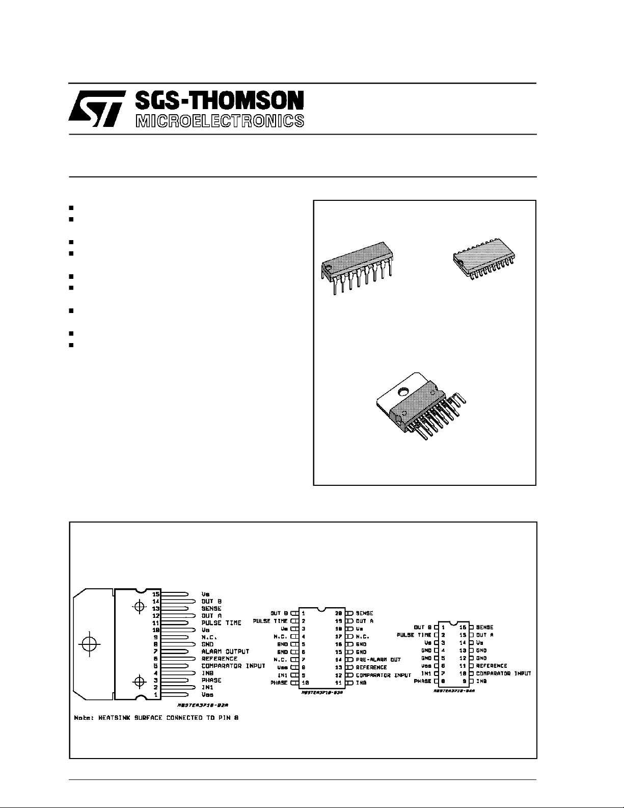
Powerdip
12+2+2
ORDERINGNUMBERS :
TEA3718SDP
TEA3718DP
MULTIWATT-15
ORDERING NUMBER : TEA3718SP
SO-20
ORDERING NUMBER :
TEA3718SFP
PIN CONNECTI O NS (top views)
TEA3718SP
(Multiwa tt -1 5)
December 1991
Thisis advanced informationon a new product now in development or undergoing evaluation. Details are subject to change withoutnotice.
TEA3718SFP
(SO-20)
TEA3718DP
TEA3718SDP
(Powerdip 12+2+2)
1/16
Page 2
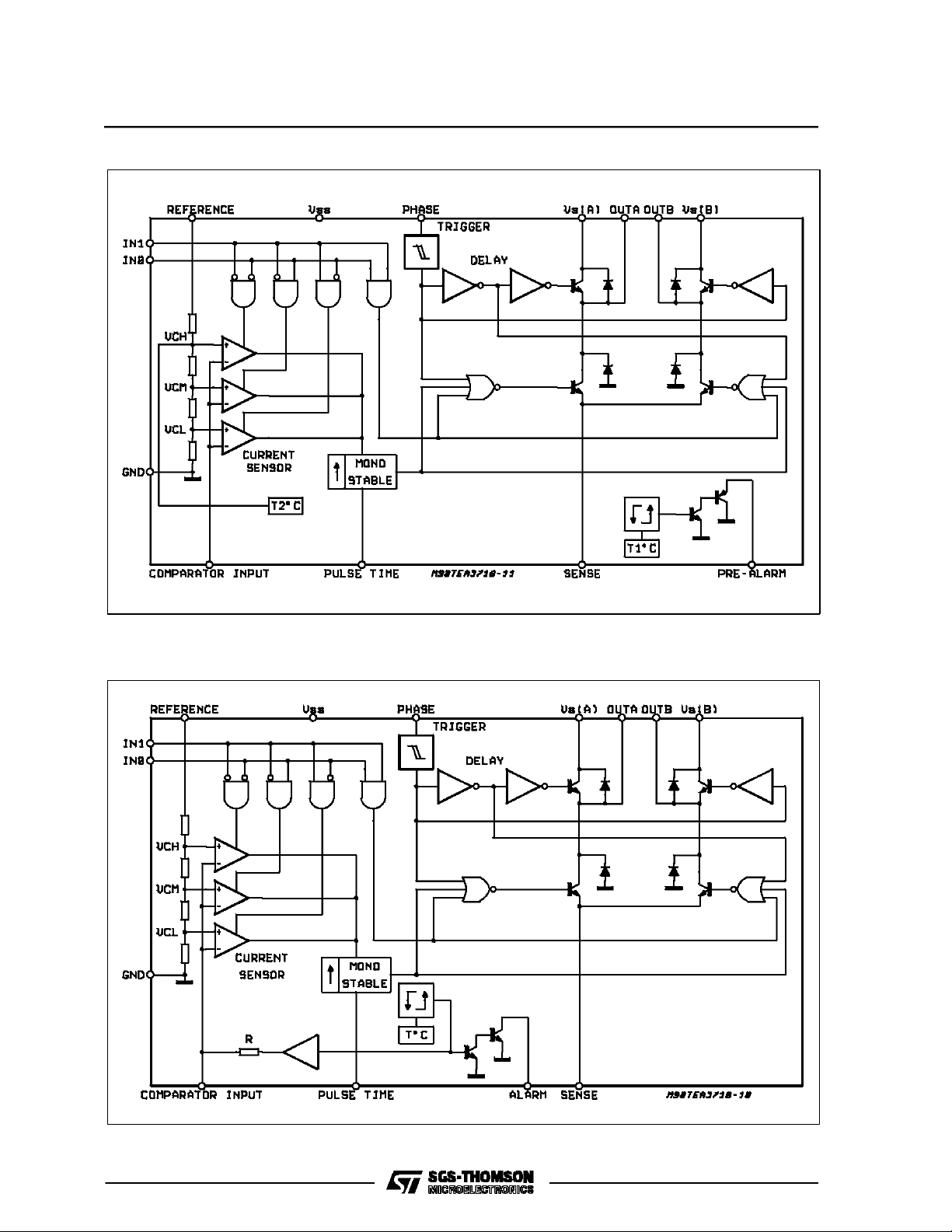
TEA371 8-TEA 3718S
BLOCK DIAGRAM TEA3718S
BLOCK DIAGRAM TEA3718
2/16
Page 3

TEA3718- TEA3718S
PIN FUNCTIONS
Name Function
OUT B Output Connection (with pin OUTA). The output stage is a ”H” bridge formed by four
transistors and four diodes suitable for switching applications.
PULSE TIME A parallel RC network connected to this pin sets the OFF time of the lower power
transistors. The pulse generator is a monostable triggered by the rising edge of the
output of the comparators (t
(B) Supply Voltage Input for Half Output Stage
V
S
GND Ground Connection. In SO-20L and Powerdip these pins also conduct heat from die
to printed circuit copper.
V
SS
Supply Voltage Input for Logic Circuitry
IN1 This pin and pin IN0 are logic inputs which select the outputs of three comparators to
set the current level. Current also depends on the sensing resistor and reference
voltage. See truth table.
PHASE This TTL-compatible logic input sets the direction of current flow through the load. A
high level causes current to flow from OUT A (source) to OUT B (sink). A Schmitt
trigger on this input provides good noise immunity and a delay circuit prevents output
stage short circuits during switching.
IN0 See INPUT 1
COMPARATOR INPUT Input connected to the three comparators. The voltage across the sense resistor is
feedback to this input through the low pass filter R
are disabled when the sense voltage exceeds the reference voltage of the selected
comparator. When this occurs the current decays for a time set by R
.
R
TCT
REFERENCE A voltage applied to this pin sets the reference voltage of the three comparators.
Reference voltage with the value of R
the output current.
(A) Supply voltage input for half output stage
V
S
OUT A See pin OUT B
SENSE RESISTOR Connection to lower emitters of output stage for insertion of current sense resistor
ALARM When T
PRE-ALARM When T
reaches T1°C the alarm output becomes low (TEA3718SP)
j
reaches T2°C the prealarm output becomes low (T2<T1) (TEA3718SFP)
j
= 0.69 RTCT).
off
. The lower power transistor
CCC
TCT,Toff
and the two inputs IN0 and IN1 determines
S
= 0.69
3/16
Page 4
TEA371 8-TEA 3718S
ABSOLUTE MAXIMUM RATINGS
Symbol Parameters Value Unit
V
T
THERMAL DAT A
Symbol Parameter SO-20L Powerdip Multiwatt Unit
R
R
*
Solderedon a 35 µm thick4 cm
Supply Voltage 7
SS
V
S
Input Voltage:
V
I
Logic Inputs
Analog Inputs
Reference Input
Input Current
i
i
Logic Inputs
Analog Inputs
Output Current ±1.5 A
I
O
Junction Temperature +150 °C
T
J
Operating Ambient Temperature Range 0 to 70 °C
T
op
Storage Temperature Range -55 to +150 °C
stg
(j-c) Maximum Junction-case Thermal Resistance 16 11 3
th
(j-a) Maximum Junction-ambient Thermal Resistance 60 * 45 * 40
th
2
PC boardcopper area.
50
V
15
-10
-10
6
SS
°C/W
°C/W
V
V
V
V
V
mA
mA
RECOMMENDED OPERATING CONDITIONS
Symbol Parameter Min. Typ. Max. Unit
v
V
i
m
T
amb
t
t
Supply Voltage 4.75 5 5.25 V
ss
Supply Voltage 10 – 45 V
S
Output Current 0.020 – 1.2 A
Ambient Temperature 0 70 °C
Rise Time Logic Inputs – – 2 µs
r
Fall Time Logic Inputs – – 2 µs
f
COMPARISON TABLE
Device Curren t P ackag e Alarm Pre-Alarm
TEA3718SDP 1.5A Powerdip 12+2+2 not connected
TEA3718SFP 1.5A SO-20L x
TEA3718SP 1.5A Multiwatt-15 X
TEA3718DP 1.5A Powerdip 12+2+2 not connected
4/16
Page 5
MAXIMUM POWER DISSIPATION
TEA3718- TEA3718S
Figure 1.
Figure 2.
RS=1 Ω INDUCTANCEFREE
R
= 470 Ω
C
C
= 820pF CERAMIC
C
R
=56kΩ
t
C
= 820 pF CERAMIC
t
P = 500 Ω
R
=1K
2
5/16
Page 6

TEA371 8-TEA 3718S
ELECTRICAL CHARACTERISTICS (VCC= 5V, ± 5%, Vmm= 10V to 45V, T
=25°C for TEA3718FP/SFP)unless otherwise specified)
(T
amb
= 0 to 70°C
amb
Symbol Parame t er Min. Typ. Max. Unit
Supply Current - - 25 mA
I
CC
High Level Input Voltage - Logic Inputs 2 - - V
V
IH
Low Level Input Voltage - Logic Inputs - - 0.8 V
V
IL
High Level Input Current - Logic Inputs - - 20 µA
I
IH
Low Level Input Current - Logic Inputs (VI = 0.4V) -0.4 - - mA
I
IL
V
CH
V
CM
V
CL
I
CO
I
off
V
sat
P
tot
t
off
t
d
V
sat
I
ref
V
sat
Comparator Thershold Voltage (VR = 5V) IO=0
=0
I
O
=0
I
O
I
=0
1
=0
I
1
=1
I
1
Comparator Input Current -20 - 20 µA
Output Leakage Current (IO=0, I1=1T
=25°C - - 100 µA
amb
Total Saturation Voltage Drop (Im = 1A) SO20/Powerdip
Multiwatt
Total Power Disssipation - Im= 1A, fs= 30KHz - 3.1 3.6 W
Cut off Time (see figure 1 and 2, Vmm= 10V, V
Turn off Delay (see fig. 1 and 2, T
=25°C, dVC/dt>50mV/µs) - 1.6 - µs
amb
>5µs 253035ms
ton
Alarm Output Saturation Voltage - IO= 2mA (Multiwatt) - 0.8 - V
Reference Input Current, VR= 5V - 0.4 1 mA
Source Diode Transistor Pair Saturation
Voltage
Powerdip Im= 0.5A
Powerdip I
m
=1A
390
230
65
-
-
-
-
420
250
80
-
-
1.05
1.35
440
270
90
2.8
3.2
1.2 (1.3)
1.5 (1.7)
mV
mV
mV
V
V
V
V
Diode Forward Voltage If= 0.5A
V
f
Substrate Leakage Current If=1A - - 5 mA
I
sub
V
Sink Diode Transistor Pair Saturation
sat
Voltage
Diode Forward Voltage If= 0.5A
V
f
Notes:
(...) Only for TEA3718SFP mounted in SO-20L package.
Multiwatt I
Multiwatt I
= 0.5A
m
m
I
f
=1A
=1A
Powerdip Im= 0.5A
Powerdip I
Multiwatt I
Multiwatt I
=1A
m
= 0.5A
m
m
=1A
I
f
=1A
-
-
-
-
-
-
-
-
-
-
-
-
1.1
1.25
1
1.2
-
-
1
1.1
1.3
1.7
1.5 (1.6)
1.7 (1.9)
1.2 (1.3)
1.3 (1.5)
1.3
1.5
1.4 (1.6)
1.5 (1.9)
V
V
V
V
V
V
V
V
V
V
6/16
Page 7

TEA3718- TEA3718S
7/16
Page 8

TEA371 8-TEA 3718S
FUNCTIONAL BLOCKS
Figure A: ALARM OUTPUT (TEA3718SP - TEA3718DP)
TEA3718
Figure B: PRE-ALARMOUTPUT (TEA3718SDP- TEA3718SFP)
TEA3718S
8/16
Page 9

TEA3718- TEA3718S
ALARM OUTPUTS (TEA3718SP- TEA3718DP)
The alarm output becomes low when the junction temperature reaches T°C.
When an alarm condition occours, parts of the
supply voltage (dividing bridge R - R
) is fed to
C
the comparator input pin (Fig. A)
Depending of the R
C value the behaviour of
C
the circuit is different on alarm condition:
>80Ω⇒the output stage is switched off
1) R
C
>60Ω⇒the current in the motor windings
2) R
C
is reduced according to the approximate formula:
(see also fig. E and F)
V
=
I
m
R
TH
V
−
R + R
S
CC
R
C
•
R
C
S
Figure C: Alarm Detection for Powerdip Package
with V
V
CM,VCL
= Threshold of the comparator (VCH,
TH
) R = 700Ω (typical)
For several Multiwatt packages a common detection can be obtained as in Fig. D
PRE-ALARM OUTPUT
When the junction temperature reaches T1°C
(typ. = 170°C) a prealarm signal is generated.
Soft thermal protection occours when function
temperaturereaches T2 (T2 > T1)
Figure D: CommonDetectionfor Several Multiwatt Package
9/16
Page 10

TEA371 8-TEA 3718S
Figure E: (typical curve) Current Reduction in
the Motor on Alarm Condition.
Notes: 1. Resistance values given here are for the Vchthreshold. They should be adjusted using other comparators threshold or other
V
value.
ref
Figure F: (V
rent on Alarm Condition.
5V) Block Diagram for Half Cur-
ref
TYPI CAL APP LI CAT IO N
10/16
Phase A
IN0A
IN1A
Phase B
IN0B
IN1B
Page 11

FUNCTIO NAL DE S CRIPTIO N
The circuitisintended todrive a bipolarconstantcurrentthroughonemotorwinding.Theconstantcurrent
is generatedthroughswitc h moderegulation.
Thereisachoiceofthreedifferentcurrentlevelswith
the two logic inputs lN0 and lN1. The current can
also beswitchedoff completely.
INPUTLOGIC
If any of the logic inputsis left open, the circuitwill
treatit asa high levelinput.
IN0 IN1 Current Level
H
H
No Current
L
H
Low Current
H
L
Medium Current
L
L
Maximum Current
PHASE- Thisinputdeterminesthedirectionof current flow in the winding, depending on the motor
connections.The signal is fed through a Schmidttriggerfor noiseimmunity,andthrougha timedelay
in order to guaranteethat no short-circuitoccurs in
the output stage during phase-shift. High level on
thePHASEinputcausesthemotorcurrentflowfrom
Out A through thewindingto Out B.
andlH1- The currentlevel in the motor winding
l
H0
is selectedwith these inputs.The valuesof the different current levels are determined by the referencevoltageV
ing resistor R
togetherwiththevalueofthesens-
R
.
S
CURRENTSENSOR
Thispart containsa currentsensingresistor (RS),a
lowpassfilter(R
) andthreecomparators.Only
C,CC
one comparatorisactiveat a time. It isactivatedby
the inputlogicaccordingtothe currentlevelchosen
with signals IN0 and IN1. The motor current flows
throughthe sensingresistor R
has increased so that the voltage across R
. Whenthe current
S
S
becomes higher than the reference voltage on the
othercomparatorinput,thecomparatoroutputgoes
high,whichtriggersthe pulsegeneratorandits output goes high during a fixed pulse time (t
), thus
off
switching off the power feed to the motor winding,
and causing the motor current to decreaseduring
.
t
off
TEA3718- TEA3718S
Thesinglepulse switchesoff the powerfeed to the
motor winding, causing the winding current to decreaseduringt
If a new trigger signal should occur during t
ignored.
OUTPUT STAGE
The output stage contains four Darlington transis-
torsandfourdiodes,connectedin anH-bridge.The
twosinkingtransistorsare usedto switchthe power
suppliedto the motor winding, thus driving a constant current through thewinding.
It should be noted however, that it isnot permitted
toshort circuit the outputs.
V
SS,VS,VR
Thecircuit will stand anyorder of turn-onor turn-off
the supply voltages V
uesare then assumed.
Preferably,V
onand power-offif V
ANALOGCONTROL
Thecurrentlevelscan bevaried continuouslyif V
is varied with a circuit varying the voltage on the
comparatorterminal.
POWER LOSSES V
.
off
off
and VS. Normal dV/dt val-
SS
shouldbetrackingVSSduringpower-
R
isestablished.
S
OUTPUT CURRE NT
S
,itis
R
SINGLE-PULSEGENERATOR
The pulse generator is a monostabletriggered on
the positive going edge of the comparator output.
Themonostableoutputishighduringthepulsetime,
, which is determinedby the timingcomponents
t
off
andCt.
R
t
t
= 0.69 ⋅ RtC
off
t
11/16
Page 12

TEA371 8-TEA 3718S
PRINCIPAL OPERATING SEQUENCE
APPLICATION NOTES
MOTOR SELECTION
Somesteppermotorsare notdesignedfor continu-
ous operation at maximum current. As the circuit
drivesa constantcurrentthroughthemotor,its temperaturemightincreaseexceedinglybothatlowand
high speed operation.
Also, some stepper motors have such high core
lossesthattheyare not suitedfor switchmode currentregulation.
UNUSED INPUTS
Unusedinputsshouldbeconnectedtopropervoltage
levelsin orderto get the highestnoise imm unity .
12/16
INTERFERENCE
As the circuit operates with switch mode current
regulation,interferencegenerationproblemsmight
arise in some applications. A good measuremight
thenbeto decouplethecircuitwith a 15 nF ceramic
capacitor,locatednearthepackagebetweenpower
line V
The ground leadbetween R
andground.
S
and circuit GND
S,CC
should be kept as short as possible. This applies
alsototheleadbetweenthesensingresistorR
S
and
pointS, see FUNCTIONAL BLOCKS.
Page 13

MULTIWATT15 PACKAGE MECHANICAL DATA
TEA3718- TEA3718S
DIM.
MIN. TYP. MAX. MIN. TYP. MAX.
A 5 0.197
B 2.65 0.104
C 1.6 0.063
D 1 0.039
E 0.49 0.55 0.019 0.022
F 0.66 0.75 0.026 0.030
G 1.02 1.27 1.52 0.040 0.050 0.060
G1 17.53 17.78 18.03 0.690 0.700 0.710
H1 19.6 0.772
H2 20.2 0.795
L 21.9 22.2 22.5 0.862 0.874 0.886
L1 21.7 22.1 22.5 0.854 0.870 0.886
L2 17.65 18.1 0.695 0.713
L3 17.25 17.5 17.75 0.679 0.689 0.699
L4 10.3 10.7 10.9 0.406 0.421 0.429
L7 2.65 2.9 0.104 0.114
M 4.25 4.55 4.85 0.167 0.179 0.191
M1 4.63 5.08 5.53 0.182 0.200 0.218
S 1.9 2.6 0.075 0.102
S1 1.9 2.6 0.075 0.102
Dia1 3.65 3.85 0.144 0.152
mm inch
13/16
Page 14

TEA371 8-TEA 3718S
POWERDIP16 PACKAGE MECHANICAL DATA
DIM.
MIN. TYP. MAX. MIN. TYP. MAX.
a1 0.51 0.020
B 0.85 1.40 0.033 0.055
b 0.50 0.020
b1 0.38 0.50 0.015 0.020
D 20.0 0.787
E 8.80 0.346
e 2.54 0.100
e3 17.78 0.700
F 7.10 0.280
I 5.10 0.201
L 3.30 0.130
Z 1.27 0.050
mm inch
14/16
Page 15

SO20 PACKAGE MECHANICAL DATA
TEA3718- TEA3718S
DIM.
MIN. TYP. MAX. MIN. TYP. MAX.
A 2.65 0.104
a1 0.1 0.3 0.004 0.012
a2 2.45 0.096
b 0.35 0.49 0.014 0.019
b1 0.23 0.32 0.009 0.013
C 0.5 0.020
c1 45 (typ.)
D 12.6 13.0 0.496 0.512
E 10 10.65 0.394 0.419
e 1.27 0.050
e3 11.43 0.450
F 7.4 7.6 0.291 0.299
L 0.5 1.27 0.020 0.050
M 0.75 0.030
mm inch
S 8 (max.)
15/16
Page 16

TEA371 8-TEA 3718S
Information furnished is believed to be accurate and reliable. However, SGS-THOMSON Microelectronics assumes no responsibility for
the consequences of use of such information nor for any infringement of patents or other rights of third parties which may result from its
use. No license is granted by implication or otherwise under any patent or patent rights of SGS-THOMSON Microelectronics. Specifications mentioned in this publication are subject to change without notice. This publication supersedes and replaces all information previously supplied. SGS-THOMSON Microelectronics products are not authorized for use as critical components in life support devices or
systems without express written approval of SGS-THOMSON Microelectronics.
MULTIWATTis a Registered Trademark of the SGS-THOMSON Microelectronics
Australia - Brazil - France - Germany - Hong Kong - Italy - Japan - Korea - Malaysia - Malta - Morocco - The Netherlands - Singapore -
1994 SGS-THOMSON Microelectronics - All Rights Reserved
SGS-THOMSON Microelectronics GROUP OF COMPANIES
Spain - Sweden - Switzerland - Taiwan - Thaliand - United Kingdom - U.S.A.
16/16
 Loading...