

Page 1
.HALF-STEPAND FULL-STEPMODE
.BIPOLARDRIVE OF STEPPERMOTOR FOR
MAXIMUM MOTORPERFORMANCE
.BUILT-IN PROTECTIONDIODES
.WIDERANGE OF CURRENTCONTROL 5 TO
1000mA
.WIDEVOLTAGERANGE10 TO 45 V
.DESIGNED FOR UNSTABILIZED MOTOR
SUPPLYVOLTAGE
.CURRENT LEVELS CAN BE SELECTED IN
STEPSOR VARIEDCONTINUOUSLY
DESCRIP TION
TheTEA3717is a bipolarmonolithicintegratedcircuitintendedto controland drive the current in one
windingof a bipolarsteppermotor.The circuitconsistsof an LS-TTLcompatiblelogic input, a current
sensor,amonostableandanoutputstagewithbuiltinprotectiondiodes.Two TEA3717andafewexternal componentsform a completecontroland drive
unitfor LS-TTLor microprocessor-controlled stepper motorsystems.
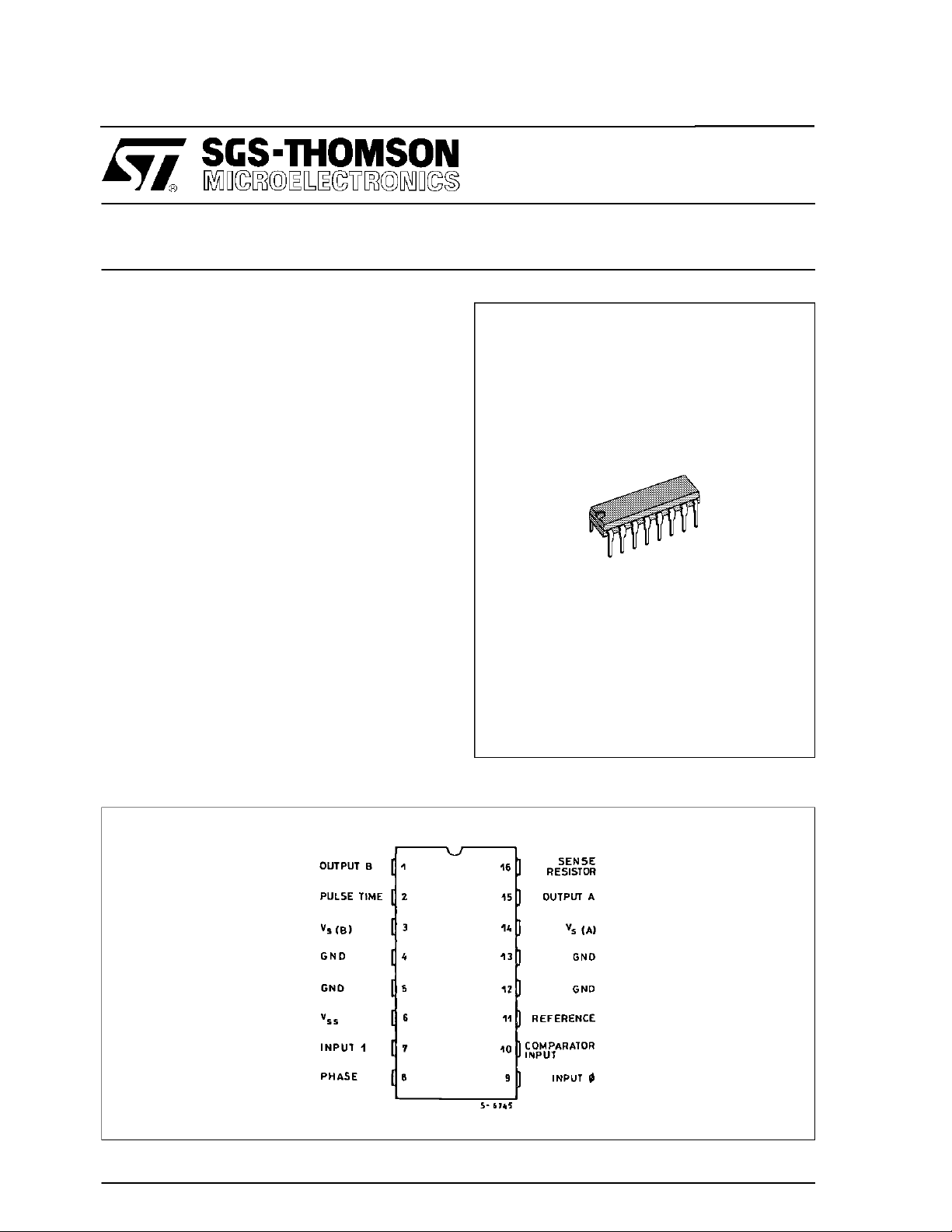
TEA3717
STEPPER MOTOR DRIVER
POWERDIP 1 2 + 2 + 2
ORDER CODE : TEA 3717D P
PIN CONNECTION (top view)
April1993
1/8
Page 2
TEA3717
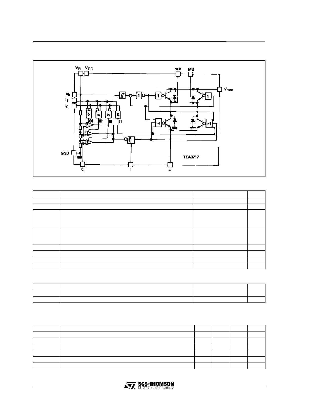
SCHEMATIC DIAGRAM
ABSOLUTE MAXIMUM RATINGS
Symbol Parameter Value Unit
V
mm
V
CC
Power Supply Voltage (pins 14, 3) 45 V
Logic Supply Voltage (pin 6) 7 V
Input Voltage
V
in
V
in
V
V
Logic Inputs
Analog Inputs
Reference Input
– 0.5 to 6
V
CC
15
Input Current
I
in
I
in
I
O
T
j
T
stg
T
oper
Logic Inputs
Analog Inputs
–10
–10
Output Current ± 1A
Junction Temperature + 150 °C
Storage Temperature Range – 55 to + 150 °C
Operating Ambiant Temperature Range 0 to + 70 °C
THERMAL DATA
Symbol Parameter Value Unit
R
th (j-c)
R
th (j-a)
*
Solderedon a 35 mm thick 20 cm
Maximum Junction-pins Thermal Resistance 11 °C/W
Maximum Junction-ambient Thermal Resistance 45* °C/W
3
PC board copperarea
RECOMMENDED OPERATING CONDITIONS
Symbol Parameter Min. Typ. Max. Unit
V
CC
V
mm
I
o
T
amb
t
r
t
f
Supply Voltage 4.75 5 5.25 V
Supply Voltage 10 – 40 V
Output Current 0.020 – 0.8 A
Ambient Temperature 0 – 70 °C
Rise Time, Logic Inputs – – 2 µs
Fall Time, Logic Inputs – – 2 µs
V
mA
2/8
Page 3

TEA3717
ELECTRICAL CHARACTERISTICS
= 5V, ±5%, Vmm= + 10V to + 40V, T
V
CC
Symbol Parameter Min. Typ. Max. Unit
I
V
V
I
I
V
V
V
I
I
V
P
t
Supply Current – – 25 mA
CC
High Level Input Voltage - Logic Inputs 2.0 – – V
IH
Low Level Input Voltage - Logic Inputs – – 0.8 V
IL
High Level Input Current - Logic Input (VI= + 2.4V) – – 20 µA
IH
Low Level Input Current - Logic Inputs (VI= + 0.4V) – 0.4 – – mA
IL
Comparator Threshold Voltage (VR= + 5.0V), I0=0,I1=0
CH
CM
CL
Comparator Input Current – 20 – 20 µA
CO
Output Leakage Current (I0=1,I1=1)
off
Total Saturation Voltage Drop (Io= 500mA) – – 4.0 V
sat
Total Power Dissipation
tot
Cut off Time (seefigure 1 and 2, Vmm= + 10V, ton≥ 5µs) 25 30 35 µs
off
Turn off Delay (see figure 1 and 2, T
t
d
=+25°C
T
amb
=+70°C, VS= 40V, VSS=5V
T
amb
= 500mA, fs= 30kHz
I
o
= 800mA, fs= 30kHz
I
o
=0oCto+70oC (unlessotherwisespecified)
amb
=1,I1=0
I
0
=0,I1=1
I
0
230
65
–
–
–
–
=+25°C, dVC/dt ≥ 50mV/µs) – 1.6 µs
amb
390
420
250
80
–
100
1.8
3.7
440
270
100
200
90
2.3
–
mV
µA
W
Figure2.Figure 1 (seenote)
3/8
Page 4

TEA3717
FUNCTIO NAL DE SCRIPTION
Thecircuitisintentedtodrivea bipolarconstantcurrentthroughone motor winding. Theconstantcurrentis generatedthroughswitch moderegulation.
Thereis achoiceofthreedifferentcurrentlevelswith
the two logic inputs l
and l1. The currentcan also
0
beswitchedoff completely.
INPUT LOGIC
If any of the logic inputs is leftopen, the circuit will
treatit as a highlevel input.
I
0
H
L
H
L
I
1
H
No Current
H
Low Current
L
Medium Current
L
Maximum Current
Current Level
PHASE− Thisinput determinesthedirectionofcurrent flow in the winding, depending on the motor
connections.The signal is fed througha Schmidttriggerfornoiseimmunity,andthrougha timedelay
in order to guaranteethat no short-circuitoccursin
the output stage during phase-shift.High level on
the PHASE-input causes the motor current flow
fromM
l
0
throughthewindingto MB.
A
andl1− Thecurrentlevel in the motor windingis
selectedwiththese inputs.The valuesof thedifferent currentlevels are determinedby the reference
voltageV
sistorR
togetherwiththevalueof the sensingre-
R
.
S
CURRENT SENS O R
Thispart containsa currentsensingresistor(R
lowpassfilter(R
)andthreecomparators.Only
C,CC
S
),a
one comparatorisactiveat atime. It is activatedby
theinput logicaccordingto thecurrentlevelchosen
with signals l
throughthe sensing resistor R
has increased so that the voltage across R
and l1. The motor current flows
0
. When the current
S
be-
S
comes higher than the reference voltage on the
othercomparatorinput,thecomparatoroutputgoes
high,whichtriggersthe pulsegeneratorandits output goes high during a fixed pulse time (t
), thus
off
switching off the powerfeed to the motor winding,
and causing the motor current to decrease during
t
off.
SINGLE-PULSE GENERATOR
The pulse generatoris a monostabletriggered on
the positive going edge of the comparatoroutput.
Themonostableoutputis highduringthepulsetime,
t
, whichis determinedby the timing components
off
and Ct.
R
t
=0.69⋅RtC
t
off
t
Thesinglepulseswitches off thepower feedto the
motor winding,causing the winding current to decreaseduring t
If a new trigger signalshould occur during t
off
.
,itis
off
ignored.
OUTPUT STAGE
The output stage contains four Darlington transistorsandfourdiodes,connectedinanH-bridge.The
two sinking transistorsare usedto switchthe powersuppliedto themotorwinding,thus drivingaconstantcurrent throughthe winding.
It should be noted however,that it is not permitted
to short circuitthe outputs.
V
CC,Vmm,VR
Thecircuit will standany orderof turn-onor turn-off
of the supply voltages V
and VS. Normal dV/dt
SS
valuesare thenassumed.
Preferably,V
shouldbetrackingVCCduringpower-
R
on and power-off.
ANALOG CONTRO L
Thecurrentlevelscan bevariedcontinuouslyeither
isvariedorwithacircuitvaryingthevoltagefed
ifV
R
intothecomparatorterminal(see fig.1).
Note : RS=1Ω, inductance free
R
=1kΩ
C
= 820pF, ceramic
C
C
=56kΩ
R
t
= 820pF, ceramic
C
t
4/8
Page 5

Figure 3
TEA3717
Functionalblocks
A. TTL compatibleinput logic
B. Current sensor
C. Single-pulse generator (monostable)
D. Outputstage withprotection diodes.
Figure4 : Typical Sink SaturationVoltageversus
OutputCurrent
Figure6 : Typical Power Lossesversus
OutputCurrent
Figure5 : TypicalSource SaturationVoltagever-
sus OutputCurrent
5/8
Page 6

TEA3717
TYPICAL APPLICATION
Figure 7 : SerialPrinter CarriageDrive.
Figure 8 : PrincipalOperatingSequence.
6/8
Page 7

POWERDIP 16 PACKAGE MECHANICAL DATA
TEA3717
DIM.
MIN. TYP. MAX. MIN. TYP. MAX.
a1 0.51 0.020
B 0.85 1.40 0.033 0.055
b 0.50 0.020
b1 0.38 0.50 0.015 0.020
D 20.0 0.787
E 8.80 0.346
e 2.54 0.100
e3 17.78 0.700
F 7.10 0.280
I 5.10 0.201
L 3.30 0.130
Z 1.27 0.050
mm inch
7/8
Page 8

TEA3717
Information furnished is believed to be accurate and reliable. However, SGS-THOMSON Microelectronics assumes no responsibility for
the consequences of use of such information nor for any infringement of patents or other rights of third parties which may result from its
use. No license is granted by implication or otherwise under any patent or patent rights of SGS-THOMSON Microelectronics. Specifications mentioned in this publication are subject to change without notice. This publication supersedes and replaces all information previously supplied. SGS-THOMSON Microelectronics products are not authorized for use as critical components in life support devices or
systems withoutexpress written approval of SGS-THOMSON Microelectronics.
1994 SGS-THOMSON Microelectronics - All Rights Reserved
Australia - Brazil - France- Germany - Hong Kong - Italy - Japan - Korea - Malaysia - Malta - Morocco - The Netherlands - Singapore -
SGS-THOMSON Microelectronics GROUP OF COMPANIES
Spain - Sweden - Switzerland- Taiwan - Thaliand - United Kingdom - U.S.A.
8/8
 Loading...