

Page 1
SWITCH MODE POWER SUPPLY CONTROLLER
.
POSITIVE AND NEGATIVE OUTPUT CURRENTUP TO 1A
.
LOW START-UPCURRENT
.
DIRECT DRIVE OF THE MOS POWER
TRANSISTOR
.
TWOLEVELS TRANSISTORCURRENTLIMITATION
.
DOUBLEPULSE SUPPRESSION
.
SOFT-STARTING
.
UNDER ANDOVERVOLTAGELOCK-OUT
.
AUTOMATIC STAND-BYMODE
.
LARGE POWER RANGE CAPABILITY IN
STAND-BY (Burst mode)
.
INTERNAL PWM SIGNAL GENERATOR
TEA2262
DESCRIPTION
The TEA2262is a monolithic integrated circuit for
the usein primarypartofanoff-lineswitchingmode
power supplyusing a MOSpower transistor.
All functionsrequired for SMPS controlunder normal operating,transientorabnormalconditionsare
provided.
The capabilityof workingaccordingto the ”masterslave” concept, or accordingto the”primary regulation” modemakesthe TEA2262very flexible and
easy to use. Thisis particularlytrue for TVreceivers wheretheICprovidesanattractiveandlowcost
solution (no need of stand-byauxiliary power supply).
PINCONNECTIONS
TRANSFORMER DEMAGNETIZATION
SENSING INPUT
SECONDARY PULSES INPUT
POWER TRANSISTOR
CURRENT LIMITATION INPUT
GROUND
GROUND
ERROR AMPLIFIER INPUT (INVERTING)
ERROR AMPLIFIER OUTPUT
OVERLOAD INTEGRATION CAPACITOR
I
max.
GND
GND
C2
1
IS
2
IN
3
4
5
6
E
7
S
8
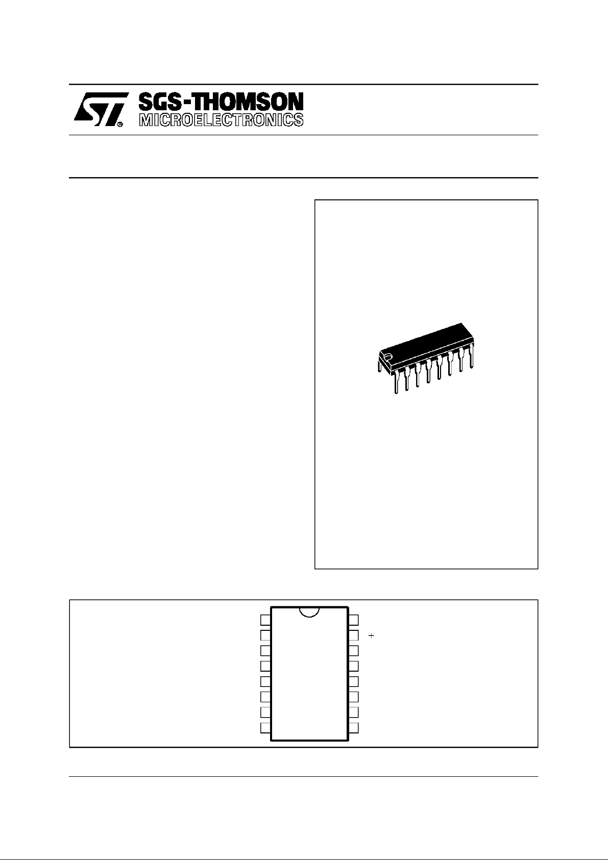
DIP16
(Plastic Package)
ORDER CODE :TEA2262
16
15
14
13
12
11
10
9
POWER SUPPLY
V
CC
POSITIVE OUTPUT STAGE SUPPLY
V
POWER OUTPUT
OUT
GROUND
GND
GROUND
GND
OSCILLATOR RESISTOR
R0
OSCILLATOR CAPACITOR
C0
SOFT-START CAPACITOR
C1
2262-01.EPS
April 1996
1/9
Page 2
TEA2262
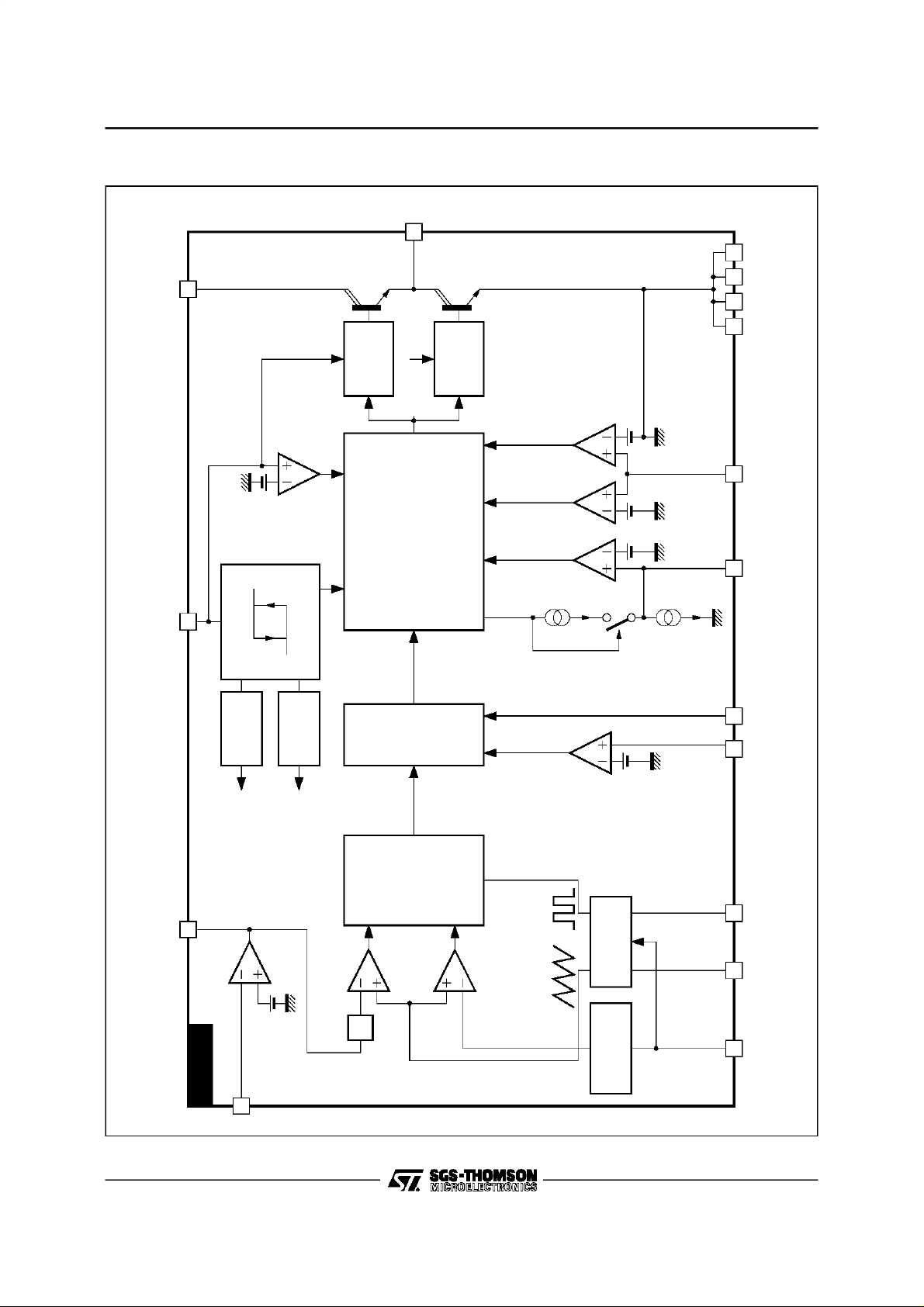
BLOCK DIAGRAM
15
V+
+1A
(Max.)
STAGE
OUTPUT
POSITIVE
OUT
14
CC
V
-1A
(Max.)
STAGE
OUTPUT
NEGATIVE
GNDI
Current
Limitation
MAX
15.7V
Protection
Overvoltage
CC
16
V
MONITORING
CC
V
8.5V 11.8V
LOGIC
PROCESSOR
Pulses
Regulation
Overload
Repetitive
Protection
45µA
2.55V 0.6V 0.84V
A
µ
10
Pulse
Secondary
2
8910
C
INIS
BIAS
INTERNAL
(2.49V)
REF
V
IS
LOGIC
12 3 45
0.15V
Pulses
Primary
Sensing
Demagnetization
S
LOGIC
MODULATOR
7
BURST
AUTOMATIC
GENERATION
0
C
f/4
Error
Amplifier
Modulators
OSCILLATOR
0
11 12 13
R
2/9
TEA2262
6
E
REF
V
2.49V
-1
(60%)
ON (Max.)
SOFT-START
T
1
C
2262-02.EPS
Page 3

TEA2262
ABSOLUTEMAXIMUM RATINGS
Symbol Parameter Value Unit
V
CC
V+ Output Stage Power Supply V15-V4, 5, 12, 13 20 V
I
OUT
I
OUT
T
T
stg
THERMAL DATA
Symbol Parameter Value Unit
R
th (j-c)
R
th (j-a)
* Solderedon a 35µm,40cm2board copper area
Figure 1 : Maximum PowerDissipation
Power Supply V16-V4, 5, 12, 13 20 V
+ Positive Output Current (source current) 1.5 A
- Negative Output Current (sink current) 1.5 A
Operating Junction Temperature 150
j
Storage Temperature -40, +150
Junction-case Thermal Resistance 15
* Junction-ambient Thermal Resistance 50
P (W)
tot
4
3
o
50 C/W
2
o
o
o
C/W
o
C/W
C
C
2262-01.TBL
2262-02.TBL
1
o
T(C)
AMB
50 100 1500
2262-03.EPS
RECOMMENDED OPERATING CONDITIONS
Symbol Parameter Min. Typ. Max. Unit
V
CC
I
OUT
I
OUT
I
OUT
I
OUT
f
oper
V
IN
R
OSC
C
OSC
C1 Soft-starting Capacitor Range 0.047 1 µF
C2 Overload Integration Capacitor 0.047 1 µF
C2/C1 Ratio C2/C1 (C2 must be ≥ C1) 1
T
amb
Power Supply VCCstop 12 VCCmax V
+ Positive Output Current (source current) 1 A
- Negative Output Current (sink current) 1 A
+ Average Positive Output Current 0.3 A
- Average Negative Output Current 0.3 A
Operating Frequency 10 150 kHz
Input Pulses Amplitude (Pin 2) 1.5 2.5 4.5 V
Oscillator Resistor Range 10 100 kΩ
Oscillator Capacitor Range 0.33 4.7 nF
Operating Ambient Temperature -20 70
o
C
2262-03.TBL
3/9
Page 4

TEA2262
ELECTRICAL CHARACTERISTICS (T
=25oC, VCC=12V, unless otherwisespecified)
amb
Symbol Parameter Min. Typ. Max. Unit
POWER SUPPLY
V
CC(start)
V
CC(stop)
Hyst V
I
CC(start)
I
CC
V
CC(max)
I
CC(over)
Starting Voltage (VCCincreasing) 9.5 11.8 13 V
Stopping Voltage (VCCdecreasing) 7 8.5 9.5 V
CC
Hysteresis (V
CC(start)-VCC(Stop)
) 2.7 3.3 3.7 V
Starting Current (VCC= 9V) 0.5 mA
Supply Current (VCC= 12V) 6.5 mA
Overvoltage Threshold on V
CC
15 15.7 V
Supply Current after Overvoltage Detection (VCC= 17V) 35 mA
OSCILLATOR / PWM SECTION
∆F
F
t
max Maximum Duty Cycle in Primary Regulation Mode 50 60 70 %
ON
Accuracy (R
= 68kΩ,C
OSC
= 1nF) 10 %
OSC
ERROR AMPLIFIER SECTION
A
VO
F
ug
I
SC
I
BE
V
REF
Open Loop Gain 75 dB
Unity Gain Frequency 550 kHz
Short Circuit Output Current (Pin 7 connected to ground) 2 mA
E Input Bias Current (Pin6) 0.08 µA
Internal Voltage Reference
2.34 2.49 2.64 V
(connected to error amplifier inputand not directly accessible)
INPUT SECTION
V
V
I
I
IN
IS
BIN
BIS
IN Input Threshold (Pin 2) 0.6 0.85 1.2 V
IS Input Threshold (Pin 1) 0.15 V
IN Input Bias Current 0.3 µA
IS Input Bias Current 0.4 µA
CURRENT LIMITATION SECTION
V
IM1
V
IM2
∆V
V
C2
I
DC2
I
CC2
I
BI(max)
First Current Limitation Threshold 550 600 650 mV
Second Current Limitation Threshold 780 840 900 mV
Thresholds Difference V
IM
IM2-VIM1
190 240 280 mV
Lock-out Threshold on Pin C2 2.25 2.55 2.85 V
Capacitor C2 Discharge Current 10 µA
Capacitor C2 Charge Current 45 µA
Maximum Input Bias Current (Pin 3) 0.2 µA
2262-04.TBL
4/9
Page 5

SIMPLIFIEDAPPLICATION DIAGRAMS
Figure1 : Master-slave Concept
TEA2262
R
MAINS
INPUT
P
C
V
CC
TEA2262
P : Output voltage adjusteme nt in normal mode
1
P : Output voltage adjustement in stand- by
2
2
SLAVE
Figure2 : SecondaryRegulation (with optocoupler)
P
1
TEA5170
MASTER
PWM
Synchronization
AUDIO
OUTPUT
STAGE
SCANNING
DEVICE
VOLTAGE
REGULATOR
Power primary ground
Secondary ground (isolated from mains)
Muting
Control
Remote
Stand-by
Remote
Stand-by
µ P
V
CC
INFRA-RED
RECEIVER
2262-04.EPS
MAINS
INPUT
P : Output voltage adjustement
R
C
V
CC
TEA2262
AUDIO
OUTPUT
STAGE
P
SCANNING
DEVICE
VOLTAGE
REGULATOR
Power primary ground
Secondary ground (isolated from mains)
Muting
Control
Remote
Stand-by
µ P
V
CC
INFRA-RED
RECEIVER
2262-05.EPS
5/9
Page 6

TEA2262
GENERALDESCRIPTION
The TEA2262 is an off-line switch mode power
supplycontroller.Thesynchronizationfunctionand
thespecificoperationin stand-bymodemakeitwell
adapted to video applications such as TV sets,
VCRs, monitors,etc...
TheTEA2262can be usedintwotypes ofarchitectures :
- Master/slave architecture. In this case, the
TEA2262drivesthepowertransistoraccordingto
the pulse width modulatedsignals generated by
the secondary located master circuit. A pulse
transformerprovidesthefeedback(seeFigure1).
- Conventional architecture with linear feedback
signal (feedbacksources : optocoupler or transformer winding) (see Figure 2).
Using the TEA2262, the stand-byauxiliary power
supply, often realized with a smallbut costly50Hz
transformer, is no longer necessary. The burst
mode operation of the TEA2262 makes possible
the control of very low output power (down toless
than 1W)with the mainpower transformer.
When used in a master/slave architecture, the
TEA2262and alsothepowertransistorturn-off can
be easily synchronized with the line transformer.
The switching noise cannot disturb the picture in
this case.
As an S.M.P.S. controller, the TEA2262 features
the followingfunctions :
- Powersupply start-up(with soft-start)
- PWM generator
- Direct powertransistor drive(±1A)
- Safety functions : pulse by pulse current limitation, outputpowerlimitation,over and undervoltage lock-out.
S.M.P.S. OPERATINGDESCRIPTION
StartingMode - Stand By Mode
Power for circuit supply is taken from the mains
through a high value resistor before starting. As
long as V
ofthe TEA2262is belowVCCstart,the
CC
quiescentcurrent is verylow (typically 0.5mA) and
the electrolytic capacitor across V
charged. When V
reaches VCCstart (typically
CC
is linearly
CC
11.8V),the circuit starts, generating output pulses
with a soft-starting.Then the SMPS goes into the
stand-bymode andthe output voltageis a percentage of the nominal outputvoltage (eg. 80%).
Duringstartingphase,in orderto avoidtransformer
magnetization (specially at high frequency), the
frequency oscillatoris divided by four.
At switch-on, C
chargingcurrentisdividedby four.
0
It recover its normal value when the voltage on
soft-startcapacitor reach 2.5V.
The current also recover its standard value when
the soft-start capacitor is dischargedbecause of a
burstoperating mode (starting in stand-by).
In other words, the charging current will become
and stay atits normal value, as soon as oneof the
followingevents occurs :
rearch2.5V
-V
C1
isdischarged by burst operatingmode
-C
1
For this the TEA2262 contains all the functions
required for primary mode regulation: a fixed frequency oscillator, a voltage reference, an error
amplifierand a pulsewidth modulator (PWM).
For transmission of low power with a good efficiency in stand-by,an automatic burst generation
systemis used, in orderto avoidaudible noise.
Normal Mode (secondaryregulation)
The normal operating of the TV set is obtainedby
sending to the TEA2262regulation pulses generated by a regulator located in the secondary side
of the power supply (TEA5170for example).
Thisarchitectureusesthe ”Master-slave Concept”,
advantages of which are now well-known especiallythe veryhigh efficiencyinstand-bymode, and
the accurate regulationin normal mode.
Stand-by mode or normal mode are obtained by
supplyingor notthe secondaryregulator. Thiscan
be ordonneredfor exempleby a microprocessorin
relation with theremote control unit.
Regulation pulses are applied to the TEA2262
through a small pulse-transformerto the IN input
(pin 2). This input is sensitive to positive square
pulses. The typicalthreshold of this input is0.85V.
The frequency of pulses coming from the secondary regulator can be lower or higher than the
frequency ofthe startingoscillator.
The TEA2262 has no soft-startingsystem when it
receivespulsesfromthe secondary.Thesoft-starting has to be located in the secondary regulator.
Due to the principle of the primary regulation,
pulsesgenerated by the startingsystem automatically disappearwhen the voltage delivered by the
SMPSincreases.
6/9
Page 7

TEA2262
Stand-byMode - Normal Mode Transition
During the transition there are simultaneously
pulses coming from the primary and secondary
regulators.
Thesesignalsare notsynchronizedand somecare
hasto betakentoensurethe safetyoftheswitching
power transistor.
Avery sure and simple wayconsist incheckingthe
transformerdemagnetizationstate.
- A primary pulse is taken in account only if the
transformer is demagnetized after a conduction
of thepower transistorrequiredby thesecondary
regulator.
- Asecondarypulse is takenin accountonly if the
transformer is demagnetized after a conduction
of the power transistor required by the primary
regulator.
Withthis arrangement the switching safetyarea of
the power transistor is respected and there is no
risk of transformer magnetization.
The magnetization state of the transformer is
checked by sensing the voltage across a winding
of the transformer (generallythe same which suppliesthe TEA2262). This is made byconnectinga
resistor between this winding and the demagnetizationsensing input of the circuit (pin 1).
SECURITY FUNCTIONS (seeflow-chart below)
- Undervoltage detection. This protection works
in association with the starting device ”V
CC
switch” (see paragraph Starting-mode - standby
mode). If V
is lower than VCCstop (typically
CC
8.5V)outputpulsesare inhibited,inorderto avoid
wrong operation of the power supply or bad
powertransistor drive.
- Overvoltagedetection. IfV
exceedsVCCmax
CC
(typically 15.7V) output pulses are inhibited and
the external capacitor C
is charged as long as
2
is higher than VCCstop. Restarting of the
V
CC
power supplyis obtainedby reducing V
stop except if the voltageacross C2reaches
V
CC
(typically 2.55V) (refer to ”Restart of the
V
C2
CC
below
power supply” paragraph).In this last case, the
circuit is definitivelystopped.
- Currentlimitation of thepowertransistor. The
current ismeasured bya shunt resistor.Adouble
thresholdsystem is used :
- When the first threshold (V
) is reached, the
IM1
conduction of the power transistor is stopped
until the end of the period : a new conduction
signalis neededto obtain conductionagain.
- Furthermore as long as the first threshold is
reached (it means during several periods), an
external capacitor C
voltageacross the capacitor reaches V
is charged. When the
2
C2
(typically2.55V)theoutput isinhibited.Thisis called
the ”repetitive overload protection”. If the overload diseappearsbefore V
is reached, C2is
C2
discharged, so transient overloads are tolerated.
- Second current limitation threshold (V
IM2
Whenthisthresholdisreachedtheoutputofthe
circuitis immediatly inhibited.This protectionis
helpfull in caseof hard overloadfor exampleto
avoid the magnetizationof the transformer.
- Restartof the powersupply. Afterstoppingdue
to V
IM2,VCC
Max or VCCstop triggering,restart of
the power supply can be obtainedby thenormal
operating of the ”V
quency fromV
due to V
C2
stop to VCCstart .After stopping
CC
threshold reaching, the circuit is de-
switch” VCCswitch se-
CC
finitively stopped. In this case it is necessary to
reduce V
below approximately5V to resetthe
CC
circuit. From a practical point of view, it means
that the power supplyhas to be temporarilydisconnected from any power source to get the
restart.
).
7/9
Page 8

TEA2262
SECURITY FLOW-CHART
S.M.P.S.
starting
First
thresholdreached
VIM1
N
V max
CC
reached
N
Normaloperating
C discharged
2
Y
Second
thresholdreached
VIM2
Y
S.M.P.S.stopped
Y
C charged
2
V < 2.6V
C2
N
Pulse by pulse current
limitingC charged
Y
2
V < 2.6V
C2
N
Y
N
Definitive
stopping
Reset C
discharged
Y
2
N
2262-06.EPS
8/9
Page 9

PACKAGE MECHANICAL DATA
16 PINS- PLASTICDIP
TEA2262
Dimensions
Min. Typ. Max. Min. Typ. Max.
Millimeters Inches
a1 0.51 0.020
B 0.77 1.65 0.030 0.065
b 0.5 0.020
b1 0.25 0.010
D 20 0.787
E 8.5 0.335
e 2.54 0.100
e3 17.78 0.700
F 7.1 0.280
I 5.1 0.201
L 3.3 0.130
Z 1.27 0.050
Information furnishedis believed to be accurate and reliable. However,SGS-THOMSON Microelectronics assumes no responsibility
for the consequences of use of suchinformation nor for any infringement of patents or other rights of third parties which may result
from its use. No licence isgranted by implication or otherwiseunder any patent orpatent rights of SGS-THOMSON Microelectronics.
Specifications mentioned in this publication are subject to change without notice. This publication supersedes and replaces all
information previously supplied. SGS-THOMSON Microelectronics products are not authorized for useas critical components in life
support devices or systems without express written approval of SGS-THOMSON Microelectronics.
199 SGS-THOMSON Microelectronics - All Rights Reserved
Purchase of I
2
I
C Patent.Rights to use these components in a I2C system,is granted provided that the system conforms to
Australia - Brazil - Canada - China - France -Germany - Hong Kong - Italy - Japan - Korea - Malaysia - Malta - Morocco
The Netherlands - Singapore -Spain - Sweden - Switzerland -Taiwan - Thailand - United Kingdom - U.S.A.
2
C Components of SGS-THOMSON Microelectronics,conveys a license under the Philips
2
the I
C Standard Specificationsas defined by Philips.
SGS-THOMSON Microelectronics GROUP OF COMPANIES
PM-DIP16.EPS
DIP16.TBL
9/9
 Loading...