

Page 1
COLOR TV EA S T-WEST CO RR ECT IO N
.
BUILD IN FRAME PARABOLA FROM EXTERNAL SA W-TOOTH
.
P A RA BO L A CORRECTI O N A DJUSTMENT
.
KEYST ONE CO RRECT ION AD JUSTME NT
.
LINE SI ZE A DJ US TM EN T
.
LINE DYNAMIC CORRECTION POSSIBILITY
(beam current)
.
D CLASS OUTPUT MODULATOR WITH
BUILD IN RECOVERY DIODE
.
50 OR 60Hz OPERATION
.
LOW DISSI PATION
.
FEW EXTERNAL COMPONENTS
DESCRIPTION
The TEA2031A is intended to ensure frame rate
modulated parabolic and keystone corrections to
the horizontal deflection circuitry of 110
sets.
The linear frame saw-tooth is applied to appropriate circuitry from which a corresponding parabolic
waveforms is obtained. This waveform is then fed
to a comparator together with the linear line sawtooth for co mparison. Comparator ’s output drives
the output power stage which is capable of sinking
the external coil currents of up to 0.5A.
An internal recovery diode feeds back to the power
supply the coil f ly-back current pulses of as high as
0.5A.
o
color TV
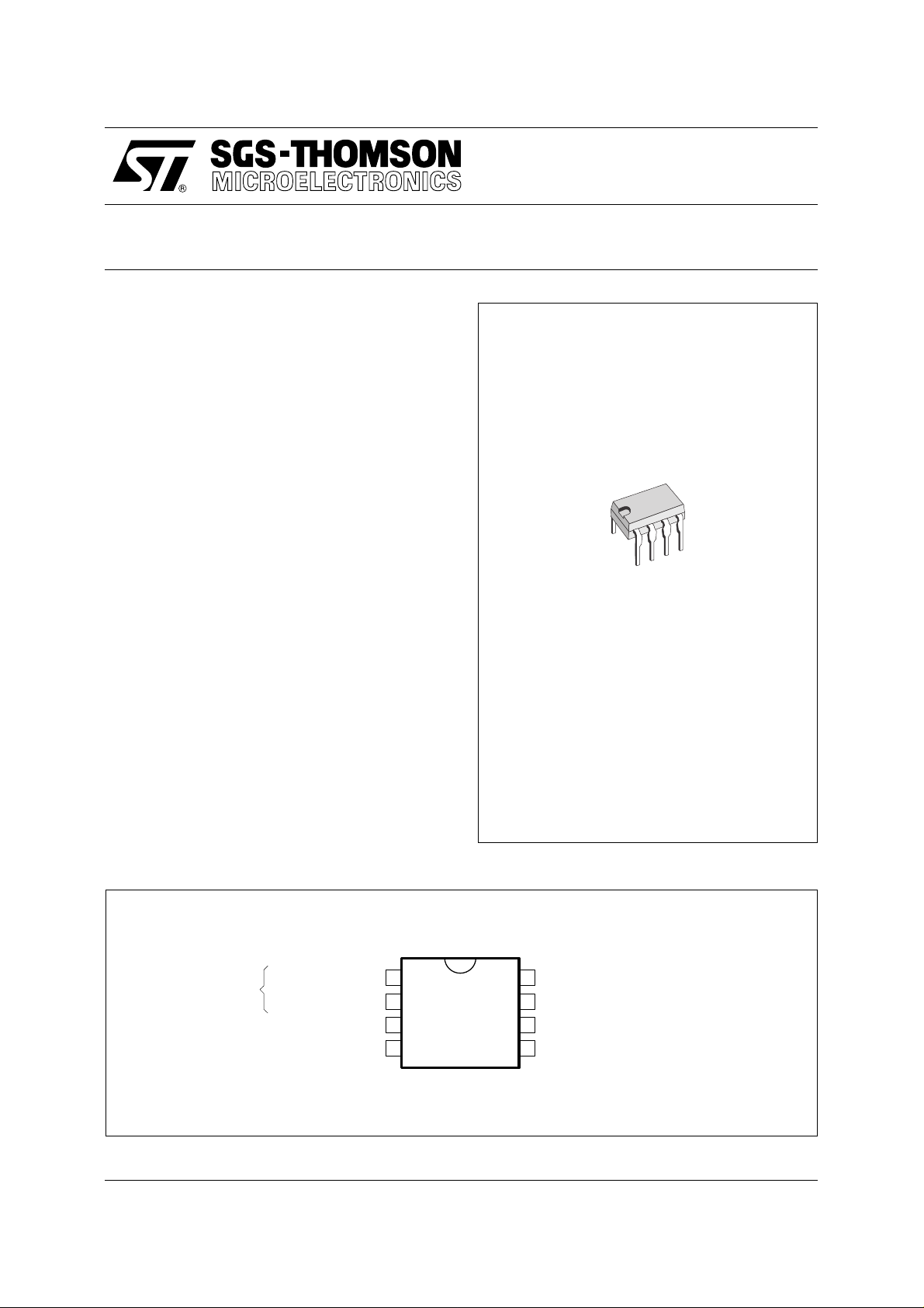
TEA2031A
DIP8
(Plastic Package)
ORDER CODE : TEA2031A
PIN CONNECTIONS
1 AND 2 CAN BE INVERTED
May 1993
MULTIPLIER INPUT 1
MULTIPLIER INPUT 2
CURRENT REFERENCE
GROUND
1
2
3
4
8
COMPARATOR INPUT 2
7
MULTIPLIER OUTPUT AND COMPARATOR INPUT 1
V POWER SUPPLY
6
CC
5
OUTPUT
2031A-01.EPS
1/6
Page 2
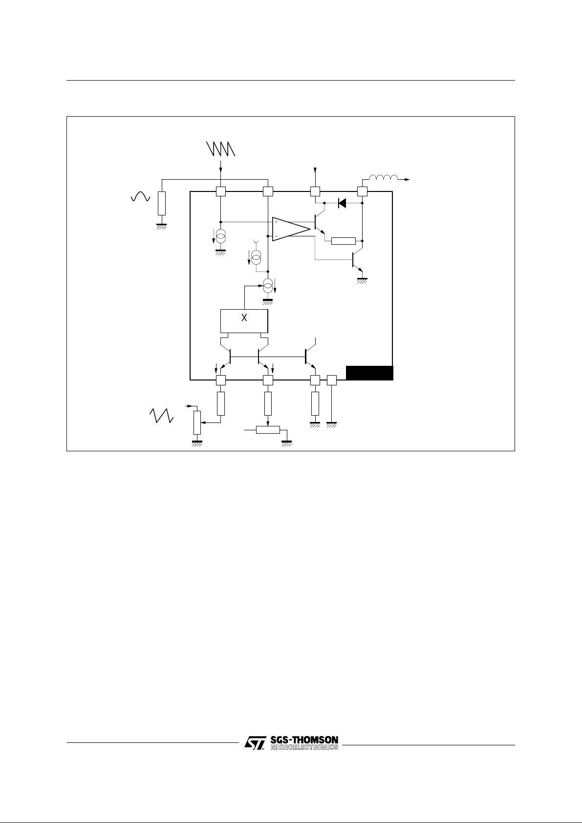
TEA2031A
BLOCK DIAG RAM
100k
Ω
Line SAW-TOOTH
50µA
120µA
+24V
V
CC
6587
Comparator
V
CC
6.8mH
To DIODE
MODULATOR
Multiplier
i
1
1234
Ω
Ω
39k
39k
DC
Frame
SAW-TOOTH
GENERAL DES CRI PTI O N
The TEA2031A is int ended to provide to 110o color
TV sets a parabolic and keystone fr ame rate modulated correction in addition to the main horizontal
scanning.
A stable 6.3V internal reference provides current
and voltage references to the whole I C.
Pins 1 and 2 are two symmetrical inputs of an
on-chip multiplier circuit and are internally held at
6.3V reference potential level. Current inputs to
these pins are drawn from external sources via
appropriate resistors. The frame saw-tooth waveform which has a peak-to-peak value of around 3
volts and a mean value of about 2.5 volt s, supplies
the required current via a series resistor t o pin 1.
Likewise, the current to pin 2 is drawn through a
series resistor from an ext ernal dc voltage s ource.
These series resistors can have values of around
40kΩ resulting in input currents of approximately
0.1mA ± modulation current.
Pin 7 should be loaded to ground through a 100kΩ
resistor which as a result will produce a parabola
12
6.3V
Ω
22k
2
TEA2031A
K . (I - I )
V
REF
i
2
of 5 volts peak-to-peak at pin 7. This parabola is
symmetrical if the DC current flowing into pin 2 is
equal to the mean input current of pin 1. Otherwise,
the parabola becomes dissymmetrical and produces a keystone effect correction.
The line saw-tooth at pin 8 is obtained by feeding
the line fly-back voltage through an integrator network formed by a diode and a grounded capacitor
(see typical application diagram). The DC component of the line saw-tooth is compe nsated by an
internal current sinking source ; so that the mean
DC values of line saw-tooth and frame parabola
voltages are equal.
Line saw-tooth and frame parabola signals are
applied to a comparator whose output is in the form
of width modulated pulses. During every pulse
duration, the output (pin 5) can sink external coil
currents of up to 0.5A associated with diode modulator of the main horizontal scanning circuit.
An internal recovery diode feeds back the fly -back
energy of the coil to the power supply. This diode
can carry currents of up to 0.5A.
2031A-02.EPS
2/6
Page 3

TEA2031A
ABSOLUTE MAXIMUM RATINGS
Symbol Parameter Value Unit
V
6–4
I
5–4
I
5–6
and I2Input Current – 0.5 mA
I
1
P
tot
T
stg
I
5–4
I
5–6
Supply Voltage 35 V
Output Sink Current 0.5 A
Diode Output Current 0.5 A
Power Dissipation 0.8 W
Storage Temperature Range – 20 to 150 °C
Non Repetitive Peak Current on Output Transistor 1.5 A
Non Repetitive Peak Current on Output Diode 1.5 A
2031A-01.TBL
THERMAL D ATA (T
= + 50°C)
amb
Symbol Parameter Value Unit
R
TH (j-a)
Junction-ambient Thermal Resistance 80 °C/W
ELECTRICAL OPERATING CHARACTERISTICS
Symbol Parameter Min. Typ. Max. Unit
V
6–4
I
6
V
3–4
I
mean Frame Saw-tooth Input DC Mean Current
1
I
1pp
I
2
∆I
V
7H
∆V
SYMMETRICAL PARABOLA FOR NO KEYSTONE EFFECT (see Figure 2)
– V
V
7H
– V7L) Parabola amplitude drift versus temperature 1 mV/°C
∆(V
7H
V
− V
7H
V
− V
7H
MAXIMUM DISSYMMETRICAL PARABOLA FOR MAXIMUM KEYSTONE EFFECT (see Figure 3)
V
– V
7H
V
− V
7H
V7H − V
DIFFERENTIAL AMPLIFIER
∆I
= F(θ) Input 8 Current Drift Versus Temperature 0.1 %/°C
8
V
5–4
V
6–5
V
5–6
Supply Voltage 16 24 35 V
Supply Current (R
No Load Consumption (R
Voltage Reference (R
= 22kΩ ; I
(3-4)
(3-4)
= 22kΩ) 5.9 6.3 6.7 V
(3-4)
= 0) 4 6 mA
OUT
= 22kΩ ; I
OUT
= 0 ; V
= 24V) 100 150 mW
(6-4)
0.1 mA
R1 = 39kΩ at 2.5V Mean - saw-tooth Voltage
Frame Saw-tooth Input Peak-to-peak Current
70 µA
R1 = 39kΩ at 2.5V Mean - saw-tooth Voltage
Keystone Correction Input DC Current
0.1 mA
If I1 Mean = I2 : No Keystone Effect. R2 = 39kΩ at 2.5V DC ref.
Keystone Correction Input DC Current for Maximum Keystone Effect ± 12.5 µA
2
Top Parabola Voltage (2V < V1 = V2 < 3V) 10 15 V
Top parabola temperature drift 0.5 mV/°C
7H
Parabola Amplitude (V2 = 2.5V ; V1 mean = 2.5V, V
7L
7L1
Symmetry 0.8 1 1.2
7L2
Parabola Amplitude (V2 = 2V or V2 = 3V ; V1 mean = 2.5V ; V
7B
7B
Parabola Amplitude Ratio 2.6 4.1
7A
= 3V) 3.5 5.2 6 V
1pp
= 3V) 5.3 8.5 9.2 V
1pp
Input 8 Sink Current Source 0.04 0.06 mA
Transfer Characteristics (pins 7-8) (F = 1MHz) 5 500 mA/mV
Input Noise (pins 7-8) 50 µV
Rise and Fall Time (louput = 250mA) 1 A/µs
Output Saturation Voltage to Ground (I5 = 0.5 A) 1.2 V
Output Saturation Voltage to VCC (I5 = 0.1A) 2 V
Output Diode Direct Voltage (I5 = + 0.5A) 1.2 V
2031A-02.TBL
2031A-03.TBL
3/6
Page 4

TEA2031A
PARABOLA OUTPUT
FIGURE 1
FIGURE 2
FIGURE 3
V
1
4V
3V
2.5V
2V
1V
0 10ms
V
7
V
7H
V7LV
7L1
0
V
7
V
7H
V
7A
10ms
20ms
V
7L2
V2= 3V
t
V V MEAN
=
12
= 2.5V
t
PARABOLA TEST DIAGRAM
V V MEAN
V
7B
= 2VV
2
10ms
V
CC
24V
100k
Ω
V
7
6587
TEA2031A
1234
22kΩ39kΩ 39kΩ
12
t
2031A-03.EPS
4/6
V
1
V
2
2031A-04.EPS
Page 5

TYPICAL APPLICATION
FLY-BACK
LINE
200V
TEA2031A
22nF
LINE SIZE
ADJUSTMENT
+3.8V
+2.5V
+1.2V
0V
4.7k
TYPICAL FRAME SAW-TOOTH
22kΩ
Ω
1.8nF
100kΩ 33kΩ 1MΩ
24V
V
CC
6587
E-W CORRECTION
EFFICIENCY (FEED-BACK)
6.3mH1N4148
To DIODE
MODULATOR
TEA2031A
1234
22kΩ39kΩ 39kΩ
I REFERENCE
3
2031A-05.EPS
2V
KEYSTONE
ADJUSTMENT
3V
5/6
Page 6

TEA2031A
PACKAGE MECHANICAL DATA
8 PINS - PLASTIC DIP
b
Z
e4
I
A
L
e3
a1
B
B1
e
E
Z
b1
D
8
5
F
14
Dimensions
Min. Typ. Max. Min. Typ. Max.
Millimeters Inches
A 3.32 0.131
a1 0.51 0.020
B 1.15 1.65 0.045 0.065
b 0.356 0.55 0.014 0.022
b1 0.204 0.304 0.008 0.012
D 10.92 0.430
E 7.95 9.75 0.313 0.384
e 2.54 0.100
e3 7.62 0.300
e4 7.62 0.300
F 6.6 02 60
i 5.08 0.200
L 3.18 3.81 0.125 0.150
Z 1.52 0.060
Information furnished i s believed to be accurate and rel iabl e. However, S GS-THOMSON Microel ectroni cs assumes no responsibil ity
for the consequences of use of such information nor for any infringement of patents or other rights of third parties which may result
from its use. No licence is granted by implication or otherwise under any patent or patent rights of SGS-THOMSON Microelectronics.
Specifications mentioned in this publication are subject to change without notice. This publication supersedes and replaces all
information previously supplied. SGS-THOMSON Microelectronics products are not authorized for use as critical components in life
support devices or systems without express written approval of SGS-THOMSON Microelectronics.
PM-DIP8.EPS
DIP8.TBL
6/6
© 1994 SGS-THOMSON Microelec tronics - All Rights Reserved
2
Purchase of I
2
C Patent. Rights to use these components in a I2C system, is granted provided that the system conforms to
I
Australia - Brazil - China - France - Germany - Hong Kong - Italy - Japan - Korea - Malaysia - Malta - Morocco
The Netherlands - Singapore - Spain - Sweden - Switzerland - Taiwan - Thailand - United Kingdom - U.S.A.
C Components of SGS-THOMSON Microelectronics, conveys a license under the Philips
2
C Standard Specifications as defined by Philips.
the I
SGS-THOMSON Microelectronics GROUP OF COMPANIES
 Loading...