

Page 1
INTEGRATED CIRCUITS
DATA SH EET
TDA1546T
Bitstream Continuous Calibration
DAC with digital sound processing
(BCC-DAC)
Preliminary specification
File under Integrated Circuits, IC01
Philips Semiconductors
January 1995
Page 2

Philips Semiconductors Preliminary specification
Bitstream Continuous Calibration DAC with
digital sound processing (BCC-DAC)
CONTENTS
1 FEATURES
1.1 Easy application
1.2 High performance
1.3 Digital sound processing features
1.3.1 Volume control features
1.3.2 Sound processing features
1.3.3 Sound monitor features
2 ORDERING INFORMATION
3 QUICK REFERENCE DATA
4 GENERAL DESCRIPTION
5 BLOCK DIAGRAM
6 PINNING
7 FUNCTIONAL DESCRIPTION
7.1 Clock generation and distribution
7.2 Power-on reset
7.3 Microprocessor interface
7.3.1 Address mode
7.3.2 Data transfer mode
7.3.3 Organization and programming of the internal
register file
7.3.3.1 Volume control register bits: BAL3 to BAL0 and
BAR3 to BAR0
7.3.3.2 Volume control register bits: VC7 to VC0 and
FT3 to FT0
7.3.3.3 Volume control register bit: MUTE
7.3.3.4 Volume control register bit: RUNFA
7.3.3.5 Sound monitor register bits: FP2 to FP0
7.3.3.6 Sound monitor register bits: OVER3 to OVER0
7.3.3.7 Sound monitor register bits: SIL3 to SIL0 and
SILT3 to SILT0
7.3.3.8 Sound monitor register bit SPOS
7.3.3.9 Sound processing register bit: DSS
7.3.3.10 Sound processing register bits: SCT3 to SCT0
7.3.3.11 Sound processing register bits: SCB3 to SCB0
7.3.3.12 Sound processing register bits: SCBB3 to
SCBB0
7.3.3.13 Sound processing register bits: DEMC1 and
DEMC0
7.3.3.14 Sound processing register bit: DSM
7.3.3.15 Miscellaneous register bits: ED3 to ED0
7.3.3.16 Miscellaneous register bits: EA2 to EA0
7.3.3.17 Miscellaneous register bits: INS1 and INS0
7.3.3.18 Miscellaneous register bits: PVIV1, PVIV0 and
PINM1, PINM0
7.3.3.19 Miscellaneous register bit: CLRM
7.3.3.20 Miscellaneous register bits: OUTS1 and
OUTS0
7.3.3.21 Miscellaneous register bit: LONLY
7.3.3.22 Miscellaneous register bits: FSO1, FSO0, TRI,
7.4 Multiple format input interface
7.4.1 Synchronization
7.5 Normal-speed mode
7.6 Double-speed mode
7.6.1 Double-speed mode features
7.6.2 Low-power option using double-speed mode
7.7 Volume control features
7.7.1 Digital balance
7.7.2 Digital volume control with fade function
7.7.3 Digital soft-mute
7.7.4 Scaling and polarity of the digital up-sampling
7.8 Sound processing related features
7.8.1 De-emphasis filter
7.8.2 Treble
7.8.3 Bass
7.8.4 Bass boost
7.8.5 Digital dynamic bass boost, digital loudness
7.8.6 Digital speaker system mode
7.9 Sound monitor block
7.9.1 Spectrum analyzer
7.9.2 dB converter
7.9.3 Peak detection
7.9.4 Silence detection
7.9.5 Overload detection
7.9.6 Versatile outputs
7.10 Noise shaper
7.11 Continuous calibration digital-to-analog
7.12 Operational amplifiers
7.13 Internal reference circuitry
8 LIMITING VALUES
9 THERMAL CHARACTERISTICS
10 QUALITY SPECIFICATION
11 CHARACTERISTICS
12 ANALOG CHARACTERISTICS
TDA1546T
ACDT, DCDT, CLKIV, CLKON, DYC1 and
DYC0
filter
and other dynamic applications of tone control
converter
January 1995 2
Page 3

Philips Semiconductors Preliminary specification
Bitstream Continuous Calibration DAC with
digital sound processing (BCC-DAC)
13 APPLICATION INFORMATION
13.1 Digital filter characteristics (theoretical values)
13.2 Example application circuit
14 PACKAGE OUTLINE
15 SOLDERING
15.1 Plastic small-outline packages
15.1.1 By wave
15.1.2 By solder paste reflow
15.1.3 Repairing soldered joints (by hand-held
soldering iron or pulse-heated solder tool)
16 DEFINITIONS
17 LIFE SUPPORT APPLICATIONS
18 PURCHASE OF PHILIPS I2C COMPONENTS
TDA1546T
January 1995 3
Page 4

Philips Semiconductors Preliminary specification
Bitstream Continuous Calibration DAC with
digital sound processing (BCC-DAC)
1 FEATURES
1.1 Easy application
• Voltage output 1.5 V (RMS)
• Operational amplifiers and cascaded 4-stage digital FIR
filter integrated
• Master and slave mode clock system with selectable
system clock (f
• I2S-bus serial input format or Japanese 16, 18 or 20 bits
serial input mode
• All features are accessible under remote control
• Simple 3-line serial microcontroller command interface
• Power-on reset
• 28 lead small outline package.
1.2 High performance
• Superior signal-to-noise ratio
• Low total harmonic distortion
• Wide dynamic range
• No zero crossing distortion
• Continuous calibration digital-to-analog conversion
combined with noise shaping techniques
• Second-order noise shaper
• 128 times oversampling in normal-speed mode
• 64 times oversampling in double-speed mode.
1.3 Digital sound processing features
1.3.1 V
• Smoothed transitions before and after digital mute (soft
mute)
• Fade function: duration-programmable (6 ms to 22.4 s
at 44.1 kHz) digital volume control (attenuation as well
as gain): +6 dB to −90 dB in steps of 0.375 dB with
automatic soft mute
• Digital balance: 0 dB to −22.5 dB in steps of −1.5 dB
(maximum overall attenuation combined with volume
control: −90 dB)
OLUME CONTROL FEATURES
) 256fs or 384f
sys
s
TDA1546T
1.3.2 S
• Digital de-emphasis filter for three sample rates (32 kHz,
44.1 kHz or 48 kHz)
• Digital treble: −10.5 dB to +12 dB at 20 kHz; 16 steps
spaced at 1.5 dB
• Digital bass: −9 dB to +13.5 dB at 20 Hz; 16 steps
spaced at 1.5 dB
• Distortion-free digital dynamic bass boost: 0 dB to
+37 dB at 10 Hz; 15 steps spaced at 2 dB
• Can be used for loudness or dynamic digital bass boost
• Double-speed mode (e.g. for high-speed dubbing)
• Pseudo double-speed mode (for power saving
application)
• Digital speaker system mode including digital crossover
filter.
1.3.3 S
• Spectrum analyzer for seven different frequency ranges
• Digital silence detection. Level (−48 dB to∞dB, in steps
of 3 dB) and duration (200 ms to 3.2 s, in steps of
200 ms at 44.1 kHz) programmable. Output via versatile
pins.
• Peak level detection and readout to microcontroller
(dB linear, 0 dB to −90 dB in steps of 1.5 dB)
• Digital overload detection. Level-programmable (dB
linear, −1.5 dB to−46.5 dB, in steps of 3 dB). Output via
versatile pins.
• Digital spectrum analyzer by combination of peak
detection and 7-band selective filter
• Optional combination spectrum analyzer and overload
detection for frequency-dependent overload detection.
OUND PROCESSING FEATURES
OUND MONITOR FEA TURES
2 ORDERING INFORMATION
TYPE
NUMBER
TDA1546T SO28 plastic small outline package; 28 leads; body width 7.5 mm SOT136-1
January 1995 4
NAME DESCRIPTION VERSION
PACKAGE
Page 5

Philips Semiconductors Preliminary specification
Bitstream Continuous Calibration DAC with
TDA1546T
digital sound processing (BCC-DAC)
3 QUICK REFERENCE DATA
SYMBOLS PARAMETER CONDITIONS MIN. TYP. MAX. UNIT
V
DD
I
DDD
I
DDA
I
DDO
I
DDX
V
FS(rms)
(THD+N)/S total harmonic distortion
S/N signal-to-noise ratio at
t
dg
BR input bit rate at data input fs= 48 kHz;
f
sys
TC
FS
T
amb
supply voltage note 1 3.8 5.0 5.5 V
digital supply current note 2 − 40 − mA
analog supply current note 2 − 5.5 − mA
operational amplifier
note 2 − 6.5 − mA
supply current
clock circuitry supply
note 2 − 1 − mA
current
full-scale output voltage
VDD= 5 V 1.425 1.5 1.575 V
(RMS value)
at 0 dB signal level −−88 −81 dB
plus noise-to-signal ratio
at −60 dB signal level;
− 0.004 0.009 %
−−44 −40 dB
A-weighted
A-weighted; at code
bipolar zero
00000H
group delay fs= sample rate;
normal-speed
100 108 − dB
−−s
24
-----f
s
−− 3.072 Ms
normal-speed
fs= 48 kHz;
−− 6.144 Ms
double-speed
system clock frequency 6.4 − 18.432 MHz
full-scale temperature
−±100× 10−6−
coefficient at analog
outputs (VOL and VOR)
operating ambient
−20 − +70 °C
temperature
−1
−1
Notes
1. All V
and VSS pins must be connected to the same supply or ground respectively.
DD
2. Measured at input code 00000H and VDD=5V.
January 1995 5
Page 6
Philips Semiconductors Preliminary specification
Bitstream Continuous Calibration DAC with
digital sound processing (BCC-DAC)
4 GENERAL DESCRIPTION
The TDA1546T is the first Bitstream Continuous
Calibration digital-to-analog converter (BCC-DAC) to
feature unique signal processing functions. In addition to
the basic functions of digital filtering and digital-to-analog
conversion, it offers such advanced digital signal
processing functions as volume control, tone control, bass
boost, peak or spectrum analyzer readout and many more
convenient functions. The digital processing features are
of high sound quality due to the wide dynamic range of the
bitstream conversion technique.
2
The TDA1546T accepts I
word lengths of up to 20 bits and various Japanese serial
data input formats with word lengths of 16, 18 and 20 bits.
The circuit can operate as a master or slave with different
system clocks (256fs or 384fs) and is therefore, eminently
suitable for use in various applications such as DCC, CD,
DAT and MD.
S-bus data input formats with
TDA1546T
The range of applications is further extended by an
incorporated Digital Speaker System mode (DSS) with
digital crossover filter.
Four cascaded FIR filters and a sample-and-hold function
increase the oversampling rate from 1f
(384fssystem clock) or 128fs (256fs system clock).
A second-order noise shaper converts this oversampled
data to a bitstream for the 5-bit DACs.
The DACs are of the continuous calibration type and
incorporate a special data coding technique, which
contributes to a high signal-to-noise ratio and dynamic
range.
On-board amplifiers convert the output current to a voltage
signal capable of driving a line output. Externally
connected capacitors perform the required first-order
filtering. Additional post filtering is not required.
to 96f
s
s
Fig.1 Digital audio reconstruction system using the TDA1546T.
January 1995 6
Page 7
Philips Semiconductors Preliminary specification
Bitstream Continuous Calibration DAC with
digital sound processing (BCC-DAC)
5 BLOCK DIAGRAM
handbook, full pagewidth
VERS1
VERS0
SPECTRUM ANALYSER
dB CONVERTER
SILENCE
DETECTION
21
VERSATILE
20
OUTPUT
BCK5WS6DATA
4
PEAK
DETECTION
OVERLOAD
DETECTION
SOURCE
SELECTION
MULTIPLE FORMAT
INPUT INTERFACE
DE-EMPHASIS
VOLUME CONTROL
BALANCE
SOFT MUTE
TONE CONTROL 1
BASS
TONE CONTROL 2
TREBLE
TONE CONTROL 3
BASS BOOST
CKSL
7
CRYSTAL
OSCILLATOR
CLOCK
GENERATION
AND
DISTRIBUTION
TDA1546T
12
XTAL1
13
XTAL2
16
CDEC
14
V
DDX
15
V
SSX
10
V
DDD
9
V
SSD
TEST1
TEST2
1 nF
C
EXT1
1 µF
V
V
GND
OL
FIR FILTER
3
11
23FILTCL
2.2 kΩ
22
26
ref
TDA1546T
LINEAR INTERPOLATOR 8f to 16f
6 x OVERSAMPLING (SAMPLE-AND-HOLD)
SECOND ORDER NOISE SHAPER
DATA ENCODER
LEFT OUTPUT SWITCHES
16 (4-bit)
R
CONV1
V
27
SSO
CALIBRATED
CURRENT
SOURCES
16 (4-bit)
CALIBRATED
CURRENT
28
V
DDO
SINKS
STAGE 1:1f to 2f
STAGE 2:2f to 4f
STAGE 3:4f to 8f
ss
REFERENCE
SOURCE
ss
FIR FILTER
ss
FIR FILTER
s
s
LINEAR INTERPOLATOR 8f to 16f
6 x OVERSAMPLING (SAMPLE-AND-HOLD)
SECOND ORDER NOISE SHAPER
RIGHT OUTPUT SWITCHES
16 (4-bit)
CALIBRATED
CURRENT
SOURCES
16 (4-bit)
CALIBRATED
CURRENT
SINKS
MICROCONTROLLER
INTERFACE
DATA ENCODER
1
V
DDA
ss
R
V
SSA
CONV2
2.2 kΩ
OP1OP1
2
8
19
18
17
24 FILTCR
25
MLC782
POR
L3DATA
L3CLK
L3MODE
V
OR
C
1 nF
EXT2
Fig.2 Block diagram.
January 1995 7
Page 8
Philips Semiconductors Preliminary specification
Bitstream Continuous Calibration DAC with
digital sound processing (BCC-DAC)
6 PINNING
SYMBOL PIN DESCRIPTION
V
DDA
V
SSA
TEST1 3 Test input 1. This pin should be
BCK 4 Bit clock input
WS 5 Word select input
DATA 6 Data input
CKSL 7 System clock frequency selection
POR 8 Power-on reset (active LOW). Internal
V
SSD
V
DDD
TEST2 11 Test input 2. This pin should be
XT AL1 12 Crystal oscillator input in master mode
XT AL2 13 Crystal oscillator drive output to crystal
V
DDX
V
SSX
CDEC 16 System clock output
L3MODE 17 Identification of the L3-bus operation
L3CLK 18 Bit clock for synchronization of
L3DATA 19 Bidirectional data line intended for
VERS0 20 Versatile output 0 for silence or
VERS1 21 Versatile output 1 for silence or
V
OL
FILTCL 23 Capacitor for left channel first-order
1 Analog supply voltage
2 Analog ground
connected to ground.
input
pull-up resistor allows timed operation
in combination with external capacitor.
9 Digital ground
10 Digital supply voltage
connected to ground.
or external clock input in slave mode
14 Crystal oscillator supply voltage
15 Crystal oscillator ground
mode
microcontroller data transfer
control data from the microcontroller
and peak data from the TDA1546T
overload detection. Can be used to
drive an LED.
overload detection. Can be used to
drive an LED.
22 Left channel audio voltage output
filter function should be connected
between this pin and V
(pin 22).
OL
TDA1546T
SYMBOL PIN DESCRIPTION
FILTCR 24 Capacitor for right channel first-order
filter function should be connected
between this pin and VOR (pin 25).
V
V
V
V
OR
ref
SSO
DDO
25 Right channel audio voltage output
26 Decoupling pin for internal reference
voltage,1⁄2V
DDA
(typ)
27 Internal operational amplifier ground
28 Internal operational amplifier supply
voltage
Fig.3 Pin configuration.
January 1995 8
Page 9
Philips Semiconductors Preliminary specification
Bitstream Continuous Calibration DAC with
digital sound processing (BCC-DAC)
7 FUNCTIONAL DESCRIPTION
The TDA1546T CMOS digital-to-analog bitstream
converter incorporates an up-sampling digital filter and
noise shaper which increase the oversample rate of 1f
input data to 128fs in the normal-speed mode. This
high-rate oversampling, together with the 5-bit DAC,
enables the filtering required for waveform smoothing and
out-of-band noise reduction to be achieved by simple
first-order analog post-filtering.
In the double-speed mode, the input sample frequency is
twice that of the normal-speed mode, as is the signal
bandwidth. The TDA1546T is able to distinguish between
the two modes (by means of a special programming bit),
so that in the double-speed mode, only half the amount of
oversampling is applied, and digital filtering is applied over
double the bandwidth compared to normal-speed. Thus in
the double-speed mode, the input sample rate of 1fs input
data is up-sampled by a factor 64f
, achieving the same
s
absolute output sample frequency as in normal-speed
mode.
In the block diagram, Fig.2, a general subdivision into main
functional Sections is illustrated. The actual signal
processing takes place in the digital signal processing
block. The two blocks named microcontroller interface and
clock generation and distribution fulfil a general auxiliary
function to the audio data processing path. The
microcontroller interface provides access to all the blocks
that require, or allow, configuration or selection and
processes the data readout from the peak detection block,
all via a simple three-line interface. The clock generation
and distribution section, which is driven by the external
system clock or crystal oscillator, provides the data
processing blocks with time bases and controls the system
mode dependent frequency settings. The following
sections give detailed explanations of the operation of
each block and their setting options processed by the
microcontroller interface, the use of the microcontroller
interface and of the operation of the clock section with its
various system settings.
s
TDA1546T
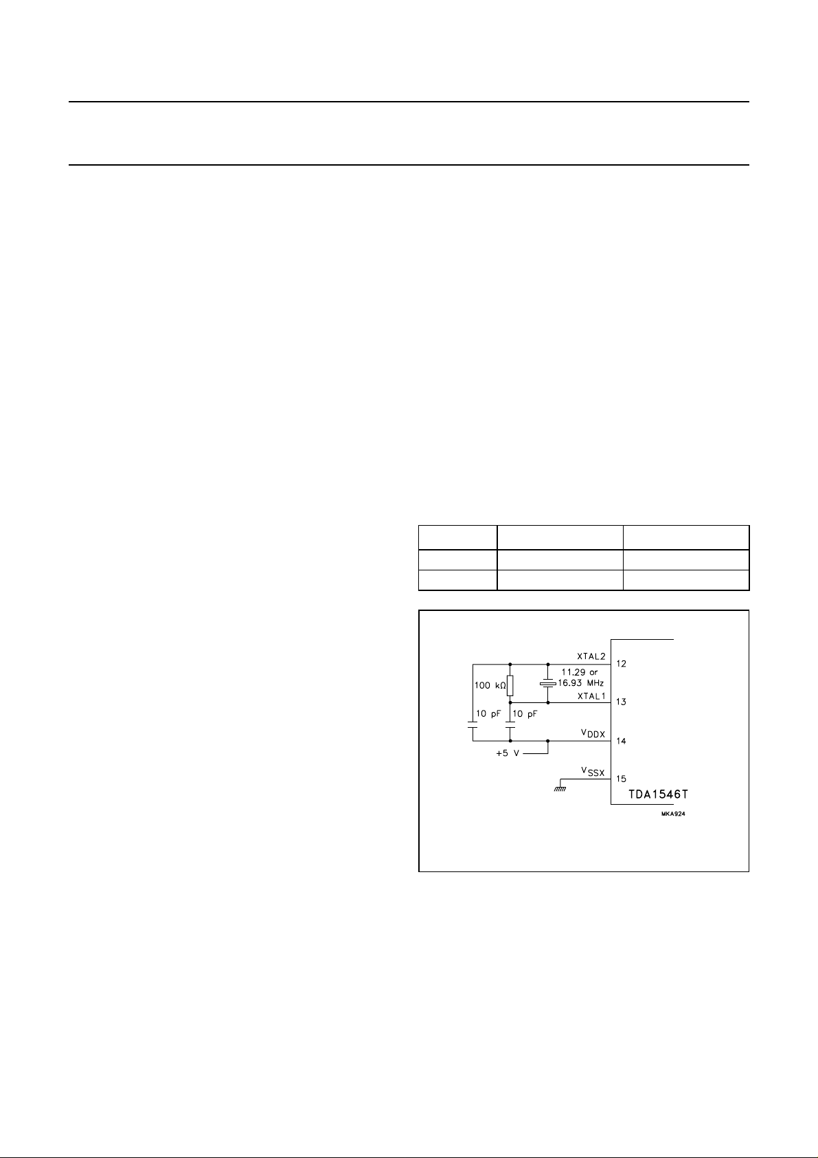
7.1 Clock generation and distribution
The TDA1546T has an internal clock generator that may
be used by connecting a crystal of 11.2896 MHz (256f
16.9344 MHz (384fs) between pins XTAL1 and XTAL2.
This mode is used when the TDA1546T is the master in
the system. The circuit diagram of Fig.4 shows the typical
connection of the external oscillator circuitry for master
mode operation.
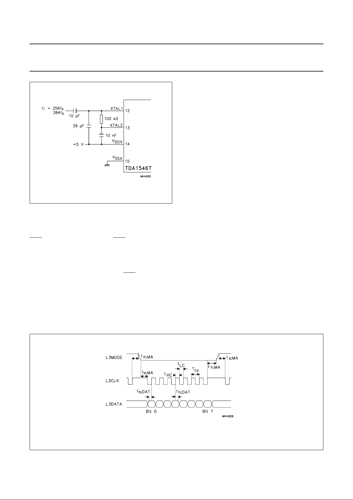
Alternatively, the TDA1546T can also operate in slave
mode. Figure 5 shows how to connect for slave mode
operation. In this mode, pin XTAL1 receives an input clock
of 256 or 384f
(fs= 32, 44.1 or 48 kHz) and voltage levels
s
of 0 V to 5 V by AC coupling and attenuation.
The CDEC output (pin 16) contains a buffered version of
the system clock for external use. The clock selection pin
CKSL is used to select between system clock frequency
ratios. Its effect is shown in Table 1.
Table 1 System clock selection
PIN CKSL SYSTEM CLOCK CDEC OUTPUT
0 256f
1 384f
s
s
256f
384f
Fig.4 External crystal oscillator circuit.
) or
s
s
s
January 1995 9
Page 10
Philips Semiconductors Preliminary specification
Bitstream Continuous Calibration DAC with
digital sound processing (BCC-DAC)
Fig.5 External clock input connection.
7.2 Power-on reset
The internal register file of the TDA1546T is initialized by a
power-on reset sequence which can be instigated via the
POR input pin 8. A LOW input on POR causes the reset
sequence to be active. This input has an internal
resistance to VDD to allow for passive use with only an
external capacitor connected between this pin and ground.
For correct detection by the TDA1546T internal controller,
the system clock must be running, andPOR should remain
LOW for at least one audio sample period before being
returned HIGH. Following detection another audio sample
period is needed to complete the initialization procedure,
after which the values of the various control bits in the
internal register file are at their predefined initial values
(see Section 7.3).
TDA1546T
7.3 Microprocessor interface
The exchange of data and control information between the
TDA1546T and a microcontroller is accomplished through
a serial hardware interface comprising the following pins:
L3DATA: microcontroller interface bidirectional data
line.
L3CLK: microcontroller interface clock line.
L3MODE microcontroller interface mode line.
Information transfer through the microcontroller bus is
organized according to the so-called ‘L3’ format, in which
two different modes of operation can be distinguished;
address mode and data transfer mode.
The address mode is required to select a device
communicating via the L3-bus and to determine the
direction of data transfer in data transfer mode. Data
transfer for the TDA1546T can be in two directions, input
to the TDA1546T to program its sound processing and
other functional features, and output from the TDA1546T
for transfer of audio peak data, which it has acquired and
processed, to the system microcontroller.
7.3.1 A
The address mode is used to select a device for
subsequent data transfer and to define the direction of that
transfer as well as the source or destination registers. The
address mode is characterized by L3MODE being LOW
and a burst of 8 clock pulses on L3CLK, accompanied by
8 data bits. The fundamental timing is shown in Fig.6.
DDRESS MODE
Fig.6 Timing address mode.
January 1995 10
Page 11
Philips Semiconductors Preliminary specification
Bitstream Continuous Calibration DAC with
digital sound processing (BCC-DAC)
Data bits 0 to 1 indicate the type of the subsequent data
transfer as shown below in Table 2. The direction of the
channel status and user data transfers depends on the
transmit/receive mode.
Table 2 Selection of data exchange
(1)
BIT 1
X 0 data to TDA1546T input
X 1 data from
Note
1. Where X = don't care.
Data bits 2 to 7 represent a 6-bit device address, with bit 7
being the MSB and bit 2 the LSB. The address of the
BIT 0 TRANSFER DIRECTION
output
TDA1546T
TDA1546T
TDA1546T is 000100 (bit 7 to bit 2). In the event that the
TDA1546T receives a different address, it immediately
3-states the L3DATA pin and deselects its microcontroller
interface logic. A dummy address of 000000 is defined for
the deselection of all devices that are connected to the
serial microcontroller bus.
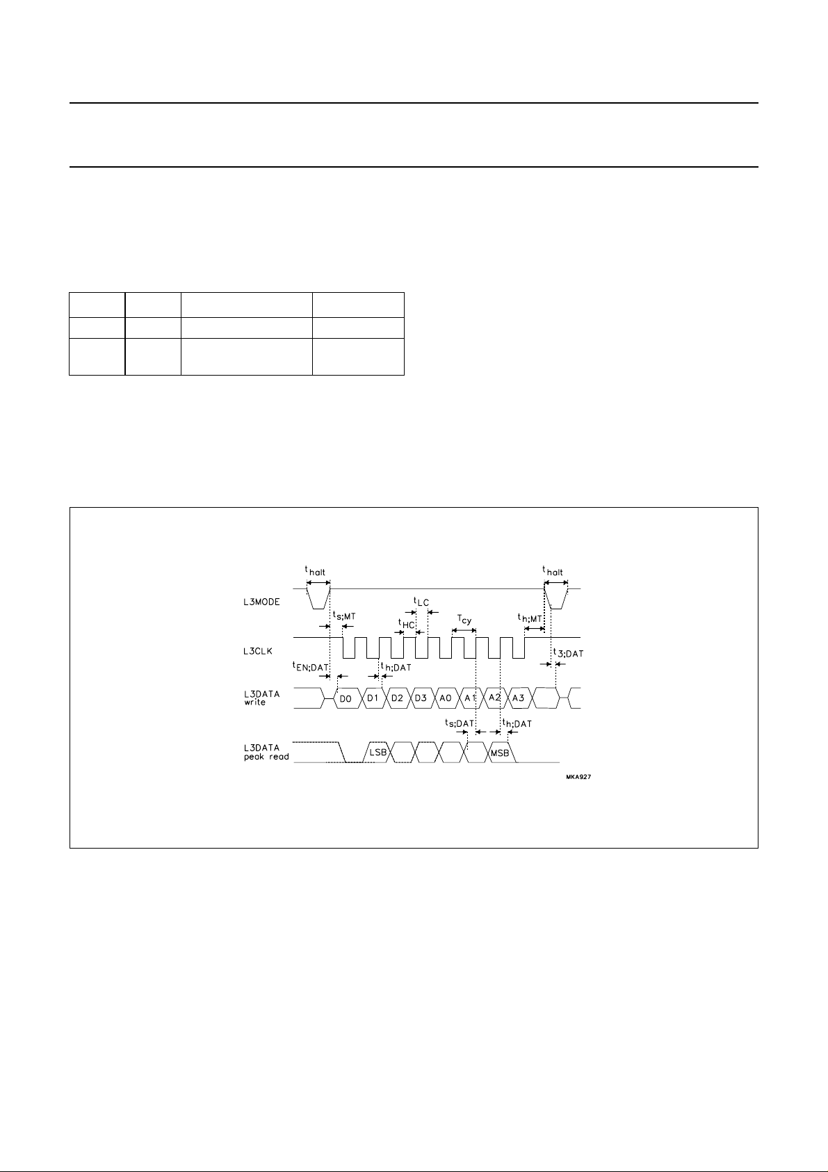
7.3.2 D
The selection performed in the address mode remains
active during subsequent data transfers, until the
TDA1546T receives a new address command. The
fundamental timing of data transfers is shown in Fig.7,
where L3DATA denotes the data from the TDA1546T to
the microcontroller (L3DATA write). The timing for the
opposite direction is essentially the same as in the address
mode (L3DATA read). The maximum input clock and data
rate is 64f
ATA TRANSFER MODE
(or 32fs when in the double-speed mode).
s
Fig.7 Timing for data transfer mode.
All transfers are bytewise, i.e. they are based on groups of
8 bits. Data will be stored in the TDA1546T after the eighth
bit of a byte has been received.
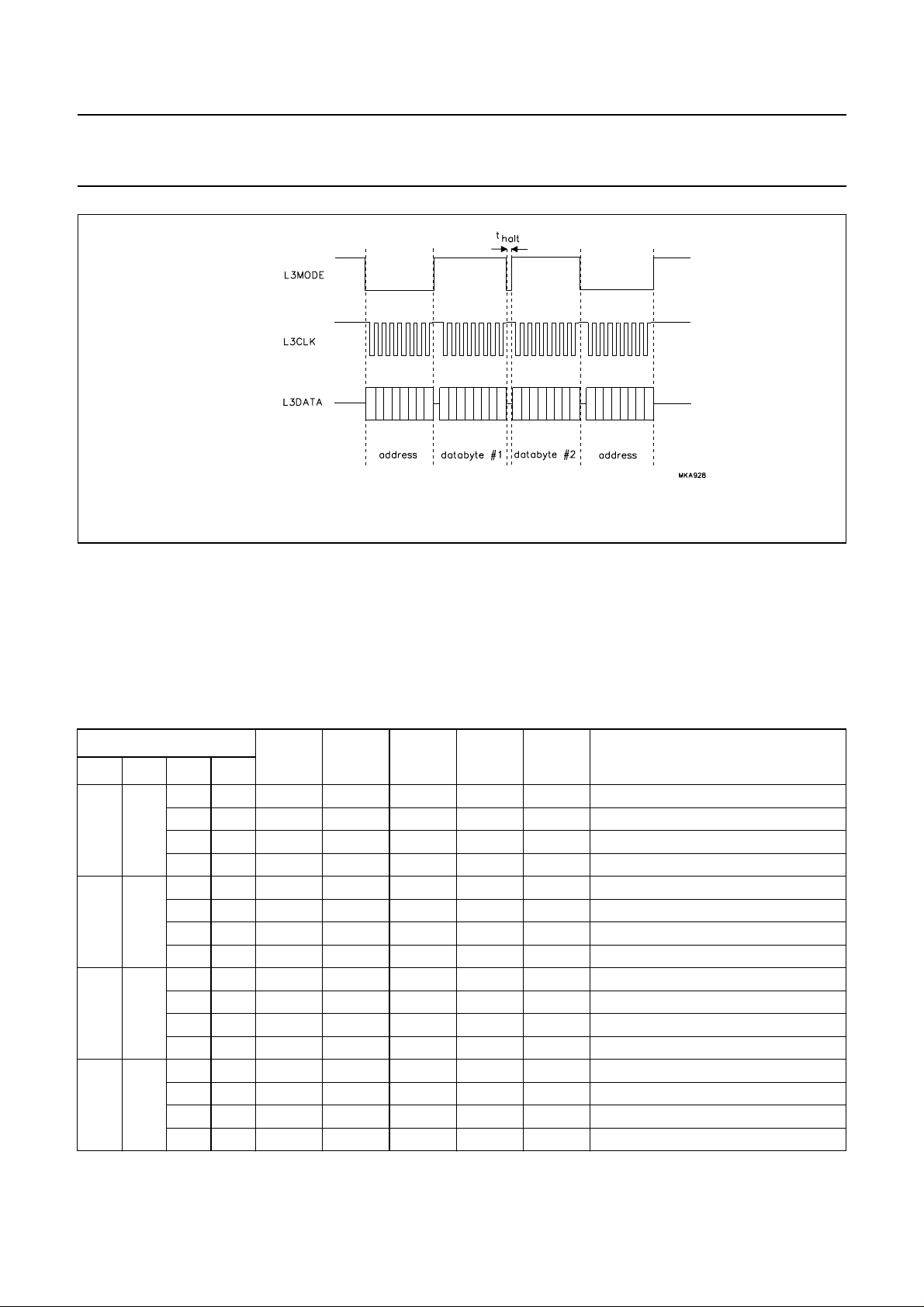
A multi-byte transfer is illustrated in Fig.8. The definition of
the L3 protocol allows for a so-called “halt” mode, as some
devices which are expected to connect to the same
microcontroller bus lines may require an indication of when
January 1995 11
8 bits have been transferred. This halt mode option is
implemented in the TDA1546T, meaning that subsequent
byte transfers must be separated by a period identified as
halt mode. A halt mode period is characterized by the
following conditions:
L3MODE = LOW, L3DATA = 3-state and L3CLK = HIGH.
Page 12
Philips Semiconductors Preliminary specification
Bitstream Continuous Calibration DAC with
digital sound processing (BCC-DAC)
Fig.8 Multibyte transfer.
7.3.3 ORGANIZATION AND PROGRAMMING OF THE
INTERNAL REGISTER FILE
Command data received from the microcontroller is stored
in an internal register file (see Table 3) which is organized
as a page of 16 registers, each containing a 4-bit
command data word (D3 to D0).
TDA1546T
Access to the words in the register file involves selection
of the address of a register location (by means of A3, A2,
A1 and A0). A second page of 4 registers is accessible by
means of the extended address register bits (EA2, EA1
and EA0) and extended data register bits (ED3, ED2, ED1
and ED0).
Table 3 Microcontroller control register file
ADDRESS
D3 D2 D1 D0
A3 A2 A1 A0
0 0 0 0 BAL3 BAL2 BAL1 BAL0 1 1 1 1 balance left
0 1 BAR3 BAR2 BAR1 BAR0 1 1 1 1 balance right
1 0 VC3 VC2 VC1 VC0 1 1 1 1 volume control
1 1 VC7 VC6 VC5 VC4 1 1 1 0 volume control
0 1 0 0 FT3 FT2 FT1 FT0 0 0 0 0 fade time
0 1 DSS FP2 FP1 FP0 0 0 0 0 digital speaker system; 3 × band-pass
1 0 OVER3 OVER2 OVER1 OVER0 1 1 1 1 overload
1 1 SIL3 SIL2 SIL1 SIL0 0 0 0 0 silence level
1 0 0 0 SILT3 SILT2 SILT1 SILT0 0 0 0 0 silence time
0 1 MUTE OUTS1 OUTS0 SPOS 0 0 0 0 mute; 2 × output scaling; peak source
1 0 SCT3 SCT2 SCT1 SCT0 0 1 1 1 treble
1 1 SCB3 SCB2 SCB1 SCB0 0 1 1 0 bass
1 1 0 0 SCBB3 SCBB2 SCBB1 SCBB0 0 0 0 0 bass boost
0 1 FSO1 FSO0 DEMC1 DEMC0 0 0 0 0 2 × reserved; 2 × de-emphasis
1 0 ED3 ED2 ED1 ED0 1 1 1 1 extended data
1 1 RUNFA EA2 EA1 EA0 1 1 1 1 run fade; extended address
INITIAL
STATE
USED FOR
January 1995 12
Page 13

Philips Semiconductors Preliminary specification
Bitstream Continuous Calibration DAC with
TDA1546T
digital sound processing (BCC-DAC)
Table 4 Extended microcontroller control register file
EXTENDED
ADDRESS
EA2 EA1 EA0
0 0 0 INS1 INS0 DSM CLRM 0 0 0 0 input format; double-speed mode;
0 0 1 PVIV1 PVIV0 PINM1 PINM0 0 0 1 0 polarity and function versatile output pins
0 1 0 LONLY TRI ACDT DCDT 0 0 1 1 left only; 3 × reserved
0 1 1 CLKIV CLKON DYC1 DYC0 0 0 0 0 4 × reserved
The following programming values for the various control
words in the register file are given below.
7.3.3.1 Volume control register bits: BAL3 to BAL0
and BAR3 to BAR0
Balance: a 4-bit value to program left channel attenuation
(BAL3 to BAL0) and a 4-bit value to program right channel
attenuation (BAR3 to BAR0). The range is
0dBto−22.5 dB in steps of 1.5 dB (see Section 7.7.1).
7.3.3.2 Volume control register bits: VC7 to VC0 and
FT3 to FT0
Volume control set number: an 8-bit value to program
volume control coefficient set (6 dB to −90 dB, in steps of
0.375 dB, VC7 to VC0); a 4-bit value to program fade time
(6 ms to 22.4 s, FT3 to FT0) (see Section 7.7.2).
7.3.3.3 Volume control register bit: MUTE
ED3 ED2 ED1 ED0
INITIAL
STATE
clear memory
7.3.3.7 Sound monitor register bits: SIL3 to SIL0 and
SILT3 to SILT0
Digital silence set numbers: a 4-bit value to program digital
silence detection level −48 dB to ∞ dB (SIL3 to SIL0) and
a 4-bit value to program digital silence duration
0.2 s to 3.2 s (SILT3 to SILT0) (see Section 7.9.4).
7.3.3.8 Sound monitor register bit SPOS
This bit controls the position of the spectrum analyzer.
When SPOS = 1 the position of spectrum analyzer
precedes the tone control sections. When SPOS = 0 the
position of the spectrum analyzer succeeds the tone
control sections.
7.3.3.9 Sound processing register bit: DSS
Digital speaker system programming bit
(see Section 7.8.6).
USED FOR
Digital soft mute control bit: logic 1 to activate mute and
logic 0 to deactivate (see Section 7.7.3).
7.3.3.4 Volume control register bit: RUNFA
Function control bit: logic 1 to activate the volume control
(after new fade time and/or volume control setting) (see
Section 7.7.2.).
7.3.3.5 Sound monitor register bits: FP2 to FP0
Frequency range control bits (see Section 7.9.1).
7.3.3.6 Sound monitor register bits: OVER3 to OVER0
Overload detection level (dB linear; 0 dB to −45 dB, in
steps of −3 dB) (see Section 7.9.5).
January 1995 13
7.3.3.10 Sound processing register bits: SCT3 to SCT0
Treble coefficient set number: a 4-bit value to program
digital treble coefficient set (see Section 7.8.2).
7.3.3.11 Sound processing register bits: SCB3 to SCB0
Bass coefficient set number: a 4-bit value to program
digital bass coefficient set (see Section 7.8.3).
7.3.3.12 Sound processing register bits: SCBB3 to
SCBB0
Bass boost coefficient set number: a 4-bit value to program
digital bass boost coefficient set (see Section 7.8.4). This
is also used for digital speaker system configuration
(see Section 7.8.6).
Page 14

Philips Semiconductors Preliminary specification
Bitstream Continuous Calibration DAC with
digital sound processing (BCC-DAC)
7.3.3.13 Sound processing register bits: DEMC1 and
DEMC0
De-emphasis function enable and fs selection bits
(see Section 7.8.1).
7.3.3.14 Sound processing register bit: DSM
Double-speed mode control bit: logic 1 to activate
double-speed mode, logic 0 to deactivate
(see Section 7.6).
7.3.3.15 Miscellaneous register bits: ED3 to ED0
Extended microcontroller control data (see Table 4).
7.3.3.16 Miscellaneous register bits: EA2 to EA0
Extended microcontroller register address (see Table 4).
7.3.3.17 Miscellaneous register bits: INS1 and INS0
Input format selection control bits (see Section 7.4).
TDA1546T
7.4 Multiple format input interface
Data input to the TDA1546T is accepted in four possible
formats, I
LSB fixed formats of word lengths 16, 18 and 20 bits. As
the resolution of the TDA1546T is 18 bits, input beyond
this number does not affect the audio data processing. The
general appearance of the permitted formats is given in
Fig.9. The selection of a format is achieved through
programming of the appropriate bits in the microcontroller
register file. The truth table for these bits, INS1 and INS0,
is given in Table 5. Characteristic timing for the input
interface is given in the diagram of Fig.9.
Table 5 Input format programming
2
S-bus (with word lengths of up to 20 bits), and
INS1 INS0 DATA INPUT FORMAT
00I
0 1 LSB-justified format, 16 bits
1 0 LSB-justified format, 18 bits
1 1 LSB-justified format, 20 bits
2
S-bus format
7.3.3.18 Miscellaneous register bits: PVIV1, PVIV0 and
PINM1, PINM0
These bits control the polarity (PVIV1 and PVIV0) and the
output mode (PINM1 and PINM0) of the versatile output
pins VERS1 and VERS0 (see Section 7.9.6).
7.3.3.19 Miscellaneous register bit: CLRM
Clear memory register bit: logic 1 to clear entire filter delay
line (approximately 2 audio samples).
7.3.3.20 Miscellaneous register bits: OUTS1 and
OUTS0
Output scaling factor control bits (see Table 10).
7.3.3.21 Miscellaneous register bit: LONLY
“Left Only” programming bit for use with digital speaker
system mode (see Section 7.8.6).
7.3.3.22 Miscellaneous register bits: FSO1, FSO0, TRI,
ACDT, DCDT, CLKIV, CLKON, DYC1 and
DYC0
Register bits reserved for future use.
7.4.1 S
For correct data input to reach the central controller of the
TDA1546T, synchronization must be achieved on the
incoming 1fs I2S-bus or LSB justified format input signals.
The incoming WS signal is sampled to detect whether its
phase transitions belonging to left channel input occur at
the correct synchronous timing instants. This sampling
occurs at the TDA1546T internal clock rate. A correct
phase transition of WS is expected after a fixed delay time
of a previous correct transition, if not, the input will be
regarded as out-of-lock. When such a condition occurs,
the internal controller is instructed to wait for a period of
16 system clock cycles during which the expected WS
transition must occur to achieve synchronization. The wait
action is repeated as often as necessary until
synchronization is achieved.
To allow for slight disturbances, which would otherwise
cause unnecessarily frequent resets, the critical WS
transitions are expected within a tolerance window (rather
than at one particular timing instant) of 32 system clock
cycles. The phase, however, may vary according to the
instant upon which synchronization has been achieved.
The word select phase transition marking the start of right
channel input data is expected after a fixed delay of the left
channel synchronized WS transition, meaning that the
input WS signal should be symmetrical in time (50% duty
cycle measured in units of system clock cycles).
YNCHRONIZATION
January 1995 14
Page 15

January 1995 15
Philips Semiconductors Preliminary specification
Bitstream Continuous Calibration DAC with
digital sound processing (BCC-DAC)
Fig.9 Input formats.
TDA1546T
Page 16

Philips Semiconductors Preliminary specification
Bitstream Continuous Calibration DAC with
digital sound processing (BCC-DAC)
TDA1546T
Fig.10 Timing of input signals.
7.5 Normal-speed mode
In the normal-speed mode the oversampling filter consists
of:
• A 75th-order half-band low-pass FIR filter which
increases the oversampling rate from 1 time to 2 times.
• An 11th-order half-band low-pass FIR filter which
increases the oversampling rate from 2 times to 4 times.
• An 7th-order half-band low-pass FIR filter which
increases the oversampling rate from 4 times to 8 times.
• A linear interpolation section which increases the
oversampling rate to 16 times. This removes the
spectral components around 8f
• A sample-and-hold section which provides another
6 times oversampling to 96 times. The zero-order hold
characteristic of this sample-and-hold section plus the
first-order analog filtering remove the spectral
components around 16fs.
.
s
7.6 Double-speed mode
The double-speed is controlled by the register control bit
DSM. When this bit is active HIGH the device operates in
the double-speed mode. In the double-speed mode the
oversampling filter consists of:
• A 51st-order half-band low-pass FIR filter which
increases the oversampling rate from 1 time to 2 times.
• A 7th-order half-band low-pass FIR filter which
increases the oversampling rate from 2 times to 4 times.
• A linear interpolation section which increases the
oversampling rate to 8 times. This removes the spectral
components around 4fs.
• A sample-and-hold section which provides another
6 times oversampling to 48 times. The zero-order hold
characteristic of this sample-and-hold section plus the
first-order analog filtering removes the spectral
components around 8fs.
January 1995 16
Page 17

Philips Semiconductors Preliminary specification
Bitstream Continuous Calibration DAC with
digital sound processing (BCC-DAC)
7.6.1 DOUBLE-SPEED MODE FEATURES
In the normal-speed mode all of the sound processing
features such as those listed in the “Features” are
available. However, the use of double-speed mode cuts
down on the number of options due to the fact that a
smaller cycle budget is available to the internal feature
controller. Table 6 gives the availability of the different
features in the double-speed mode.
Table 6 Feature status in double-speed mode
FEATURE AVAILABLE REMARKS
Balance yes
Volume yes adapted scale: range
from −96 dB to 0 dB
Fade no volume change will be
instantaneous
Band-pass
filter
Overload
detection
Silence
detection
Mute yes
Peak position no fixed to before
Treble, Bass no
Bass boost yes
De-emphasis yes
Clear
memory
Versatile pins yes although no detection
Peak readout yes
Because of the shift in scale of the volume control between
normal and double-speed mode, a step in volume of 6 dB
on switchover in either way should be compensated for by
adjusting the volume during a preferably muted transition
period.
7.6.2 L
The double-speed mode feature can also be used to cut
down on power requirements. When the TDA1546T is
switched to the double-speed mode using control bit DSM,
and the system clock frequency is halved simultaneously,
the filters will operate correctly on data input at
OW-POWER OPTION USING DOUBLE-SPEED MODE
no fixed to flat response
no
no
yes
takes place these pins
respond to polarity
setting
TDA1546T
normal-speed. The same feature restrictions as in the
double-speed mode apply, as does the filter performance
specified for double-speed mode. The current
consumption of the digital supply voltage is halved
because of the lower absolute clock speed. In terms of
conversion accuracy of the digital-to-analog converter
section, some performance will however be sacrificed.
7.7 Volume control features
Features related to volume control are the digital balance
control, digital volume control with fade function and the
digital soft-mute. Their operation is described below.
7.7.1 D
Table 7 Digital balance
The balance value from 1111 to 0000 can be obtained
using the following equation;
Balance = −1.5 dB × (15 − balance setting)
At extremely low volume settings (see Section 7.7.2) the
range of effect of the balance control will be limited. The
balance control effect will not go beyond an overall
attenuation of 89.55 dB (balance plus volume control).
7.7.2 DIGITAL VOLUME CONTROL WITH FADE FUNCTION
One of the features of the TDA1546T is an advanced
digital volume control with inherent fading function. Only
the desired volume and the fade speed need to be
instructed to the TDA1546T, via the microcontroller
interface. The single-bit flag RUNFA can then be used to
inhibit or execute the volume change operation. When
RUNFA = 0, the volume control settings can be changed
without effect on the output. When RUNFA is then set to 1,
the TDA1546T autonomously performs an automatic
fade-in or fade-out to the desired volume by a natural,
exponential approach. It allows for volume control to an
accuracy of 0.375 dB from a gain of 6 dB of full-scale to
−90 dB in normal-speed, and a range of 0 dB of full-scale
to −96 dB in double-speed mode (see Tables 8 and 9).
IGITAL BALANCE
BAL3 TO BAL0
BAR3 TO BAR0
1 1 1 1 0
1 1 1 0
....
0 0 0 1
0 0 0 0 −22.5
LEVEL (dB)
−1.5
...
−21.0
January 1995 17
Page 18

Philips Semiconductors Preliminary specification
Bitstream Continuous Calibration DAC with
digital sound processing (BCC-DAC)
In normal-speed operation the fade time can be set over a
wide range, varying from 6 ms to over 20 seconds for a
complete fade. The fade time is completely determined by
the fade time setting and is independent of the amount of
volume change programmed. This means that a smaller
volume step will take the same amount of time but using a
less steep slope than a larger volume change with the
same fade time setting.
In the double-speed mode the fade option is not available.
Regardless of the current fade speed setting, a volume
change in double-speed mode will take effect immediately,
i.e. the next audio sample instant. Volume control data is
in 2 nibbles and can be set in 256 steps. The relationship
between command and output is shown in Tables 8 and 9.
Table 8 Volume control
VC7 TO VC0 VC (DEC)
1111 1111 255 6.02 0
1111 1110
....
1111 0000
1110 1111
....
0000 0001
0000 0000 0 −∞ −∞
254
...
240
239
...
1
VOLUME LEVEL
NS DS
5.64
....
0.37
0.00
....
−89.55
−0.37
....
−5.64
−6.02
....
−95.57
TDA1546T
The gain value ranging from 1111 1111 to 0000 000 can
be converted to its logarithmic counterpart by the following
equations:
Normal-speed mode:
G volume setting 239–()
Example: attenuate data for 1111 11110:
A 254 239–()
Double speed mode:
G volume setting 255–()
Example: attenuate data for 1111 11110:
A 254 255–()
The fade time from 0000 to 1111 can be converted by
using the following equation:
Fade time
Example: fade time for 0010 at f
fade time = 3 × 33 × 256/44100 = 0.57 s
In Fig.11, a few fading examples illustrate the operation of
the TDA1546T advanced digital volume control.
=
5 log 2×
---------------------4
5 log 2×
---------------------4
FT 1+()FT 16 1+×()×[]256×
-------------------------------------------------------------------------------------------
5log2()×
×=
-----------------------------
5.64 dB=×=
5log2()×
×=
-----------------------------
f
s
= 44.1 kHz;
s
4
4
0.37 dB–=×=
Table 9 Fade control
FT3 TO FT0 FT (DEC)
0000 0 0.006
0001 1 0.2
0010
....
1110
1111 15 22.4
January 1995 18
2
...
14
FADE TIME AT
44.1 kHz (s)
0.6
....
19.6
Page 19

Philips Semiconductors Preliminary specification
Bitstream Continuous Calibration DAC with
digital sound processing (BCC-DAC)
(1) A = fade-out to zero volume (VC = 0; RUNFA = 1).
(2) B = fade-in to maximum volume (RUNFA = 0; VC = 256; RUNFA = 1).
(3) C = volume decrease (RUNFA = 0; VC = XXX; RUNFA = 1).
(4) D = volume regulation override by resetting RUNFA to 0.
(5) E = volume regulation resumed by resetting RUNFA to 1.
(6) F = volume regulation stops at programmed level XXX.
(7) G = fade-in to maximum level (RUNFA = 0; VC = 256; RUNFA = 1).
(8) H = change in fade time (RUNFA = 0; FT = xxx; RUNFA = 1).
(9) I = fade-out to lower volume level and fade time change (RUNFA = 0; new VC; new FT; RUNFA = 1).
(10) J = volume regulation stops at programmed level.
Note: for illustration only, axes vary in scale.
TDA1546T
Fig.11 Volume control example.
7.7.3 DIGITAL SOFT-MUTE
Soft mute is controlled by the microcontroller register file
bit MUTE. When the bit is active HIGH the value of the
samples is decreased smoothly to zero following a cosine
curve. To step down the value of the data 32 coefficients
are used, each one being used 32 times before stepping
onto the next. This amounts to a mute transition time of
23 ms at fs= 44.1 kHz. When the MUTE bit is LOW, the
samples are returned to the full level again following the
same cosine curve in reverse order. Mute is synchronized
to the sample clock, so that operation always takes place
on complete samples.
7.7.4 S
CALING AND POLARITY OF THE DIGITAL
-SAMPLING FILTER
UP
The scaling factor of the digital up-sampling filter can be
selected by means of register file bits OUTS1 and OUTS0.
Only those modes controlled by bit OUTS0 are actually
useful, the other two are reserved modes and should not
be used.
In the configuration with the default initialization
(OUTS0 = 0), the TDA1546T is inverting, meaning that a
positive pulse contained in the digital input data is
converted to a negative pulse on the analog outputs. This
polarity and scaling is identical to that used in TDA1305T.
The TDA1546T can be made non-inverting by setting bit
OUTS0 in the microcontroller register file. The complete
truth table for these bits is shown in Table 10.
Table 10 Special control register bits
OUTS1 OUTS0 MODE SCALING
0 0 TDA1305T equivalent −0.9
0 1 non-inverting +0.9
1 0 reserved −0.66
1 1 reserved −0.99
January 1995 19
Page 20

Philips Semiconductors Preliminary specification
Bitstream Continuous Calibration DAC with
digital sound processing (BCC-DAC)
7.8 Sound processing related features
7.8.1 D
The TDA1546T incorporates selectable digital
de-emphasis filters, dimensioned to produce the
de-emphasis frequency characteristics for each of the
three possible sample rates 32, 44.1 and 48 kHz. With its
18-bit dynamic range, the digital de-emphasis of the
TDA1546T is a convenient and component-saving
alternative to analog de-emphasis.
Selection of the de-emphasis filters is performed via the
microcontroller interface, bits DEMC1 and DEMC0. The
programming is given in Table 11.
Table 11 De-emphasis mode programming
DEMC1 DEMC0 DE-EMPHASIS FUNCTION
E-EMPHASIS FILTER
0 0 de-emphasis disabled
0 1 de-emphasis for fs= 32.0 kHz
1 0 de-emphasis for f
1 1 de-emphasis for f
= 44.1 kHz
s
= 48.0 kHz
s
TDA1546T
7.8.4 BASS BOOST
A strong bass boost effect, which is useful in
compensating for poor bass response of portable
headphone sets, is implemented digitally in the TDA1546T
and can be controlled in 14 steps using the microcontroller
bits SCBB3 to SCBB0. Valid settings range from “flat” (no
influence on audio) to +37 dB with step sizes varying from
3 dB (lower boosts) to 2.5 dB to 2 dB (higher boosts). The
SCBB value 15 is a reserved value and should not be
used. (see Table 12). The programmable bass boost filter
is a second-order shelving type with a fixed corner
frequency of 250 Hz and has a Butterworth characteristic.
Because of the exceptional amount of programmable gain,
bass boost should be used in conjunction with adequate
prior attenuation, using the volume control. The bass stage
and the bass boost stage operate independently so that
the ultimately attainable gain for low frequencies may
reach a total boost of approximately 50 dB.
7.8.5 D
IGITAL DYNAMIC BASS BOOST, DIGITAL LOUDNESS
AND OTHER DYNAMIC APPLICATIONS OF TONE
CONTROL
7.8.2 TREBLE
A digital treble gain (up to 12 dB in steps of 1.5 dB or cut
down to −10.5 dB in steps of 1.5 dB) can be applied to
boost or attenuate high-range signal content. The
microcontroller bits SCT3 to SCT0 select the treble
characteristic to be applied, the effect of which is shown in
Table 12. The programmable treble filter is a first-order
shelving type with a fixed corner frequency of 2.1 kHz. In
the “flat” position the treble stage has no influence on the
audio signal path. Because of the possibility of treble boost
beyond the available digital headroom causing overload of
high frequency range signals, the higher positive treble
boost values should generally be used in conjunction with
an approximately corresponding attenuation using the
volume control function.
7.8.3 B
Digital bass control can be applied under control from the
microcontroller via control bits SCB3 to SCB0
(see Table 12) to achieve a moderate bass enforcement
or attenuation. The programmable bass filter is a
first-order shelving type with a fixed corner frequency of
500 Hz. In the “flat” position the bass stage has no
influence on the audio signal path. Higher bass settings
should generally be compensated by approximately equal
attenuation using the volume control to avoid digital
overload of basses.
ASS
Because of the integration of volume control, tone control
and level monitoring functions in the TDA1546T, a wide
range of dynamic tone and level control applications is
made available. These can be defined in software by the
user, thereby replacing and improving on components
formerly used to perform these functions in the analog
domain. Among these applications the most popular are
dynamic bass boost and loudness. Because the volume
setting is known in the system controller, it can, for
instance, be used directly to determine an appropriate
amount of bass boost. This avoids the signal level
dependent ‘sighing’, ‘pumping’ and distortion effects
typical of analog dynamic bass boost circuits. Depending
on the headroom made available by the current volume
setting, applying a bass boost of up to 30 dB, combined
with a slight treble boost (up to 6 dB) will achieve a typical
dynamic bass boost effect of high sound quality.
Digital loudness can be realized using the current volume
setting to determine a suitable moderate bass gain (up to
approximately 15 dB is typical of loudness) and treble gain
(up to approximately 6 dB).
A further enhancement in dynamic tone control and signal
adaptation can be achieved by using the peak monitoring
function (either with a flat response or using the band-pass
filters) or overload detection (which can also be made
frequency-selective) in your dynamic tone control
algorithm.
January 1995 20
Page 21

Philips Semiconductors Preliminary specification
BBBBBBBBBBBBBBBBBBBBBBBBBBBBBBBBBBBBBBBBBBBBBBBBBBBBBBBBBBBBBBBBBBBBBBBBBBBBBBBBBBBBBBBBBBBBBBBBBBB
B
B
B
B
B
B
B
B
B
B
B
B
B
B
B
B
B
B
B
B
B
B
B
B
B
B
B
B
B
B
B
B
B
B
B
B
B
B
B
B
B
B
B
B
B
B
B
B
B
B
B
B
B
B
B
B
B
B
B
B
B
B
B
B
B
B
B
BBBBBBBBBBBBBBBBBBBBBBBBBBBBBBBBBBBBBBBBBBBBBBBBBBBBBBBBBBBBBBBBBBBBBBBBBBBBBBBBBBBBBBBBBBBBBBBBBBB
Bitstream Continuous Calibration DAC with
digital sound processing (BCC-DAC)
Table 12 Sound processing parameters
REGISTER BITS
TREBLE SCT3 TO SCT0
(dB)
0 0 0 0 −10.5 −9 flat
0 0 0 1 −9 −7.5 3
0 0 1 0 −7.5 −66
0 0 1 1 −6 −4.5 9
0 1 0 0 −4.5 −312
0 1 0 1 −3 −1.5 15
0 1 1 0 −1.5 flat 18
0 1 1 1 flat 1.5 21
1 0 0 0 1.5 3 23.5
1 0 0 1 3 4.5 26
1 0 1 0 4.5 6 28.5
1 0 1 1 6 7.5 31
1 1 0 0 7.5 9 33
1 1 0 1 9 10.5 35
1 1 1 0 10.5 12 37
1 1 1 1 12 13.5 reserved
BASS SCB3 TO SCB0
(dB)
TDA1546T
BASS BOOST SCBB3 TO SCBB0
(dB)
BBBBBBBBBBBBBBBBBBBBBBBBBBBBBBBBBBBBBBBBBBBBBBBBBBBBBBBBBBBBBBBBBBBBBBBBBBBBBBBBBBBBBBBBBBBBBBBBBB
BBBBBBBBBBBBBBBBBBBBBBBBBBBBBBBBBBBBBBBBBBBBBBBBBBBBBBBBBBBBBBBBBBBBBBBBBBBBBBBBBBBBBBBBBBBBBBBBBB
BBBBBBBBBBBBBBBBBBBBBBBBBBBBBBBBBBBBBBBBBBBBBBBBBBBBBBBBBBBBBBBBBBBBBBBBBBBBBBBBBBBBBBBBBBBBBBBBBB
BBBBBBBBBBBBBBBBBBBBBBBBBBBBBBBBBBBBBBBBBBBBBBBBBBBBBBBBBBBBBBBBBBBBBBBBBBBBBBBBBBBBBBBBBBBBBBBBBB
BBBBBBBBBBBBBBBBBBBBBBBBBBBBBBBBBBBBBBBBBBBBBBBBBBBBBBBBBBBBBBBBBBBBBBBBBBBBBBBBBBBBBBBBBBBBBBBBBB
BBBBBBBBBBBBBBBBBBBBBBBBBBBBBBBBBBBBBBBBBBBBBBBBBBBBBBBBBBBBBBBBBBBBBBBBBBBBBBBBBBBBBBBBBBBBBBBBBB
BBBBBBBBBBBBBBBBBBBBBBBBBBBBBBBBBBBBBBBBBBBBBBBBBBBBBBBBBBBBBBBBBBBBBBBBBBBBBBBBBBBBBBBBBBBBBBBBBB
BBBBBBBBBBBBBBBBBBBBBBBBBBBBBBBBBBBBBBBBBBBBBBBBBBBBBBBBBBBBBBBBBBBBBBBBBBBBBBBBBBBBBBBBBBBBBBBBBB
BBBBBBBBBBBBBBBBBBBBBBBBBBBBBBBBBBBBBBBBBBBBBBBBBBBBBBBBBBBBBBBBBBBBBBBBBBBBBBBBBBBBBBBBBBBBBBBBBB
BBBBBBBBBBBBBBBBBBBBBBBBBBBBBBBBBBBBBBBBBBBBBBBBBBBBBBBBBBBBBBBBBBBBBBBBBBBBBBBBBBBBBBBBBBBBBBBBBB
BBBBBBBBBBBBBBBBBBBBBBBBBBBBBBBBBBBBBBBBBBBBBBBBBBBBBBBBBBBBBBBBBBBBBBBBBBBBBBBBBBBBBBBBBBBBBBBBBB
BBBBBBBBBBBBBBBBBBBBBBBBBBBBBBBBBBBBBBBBBBBBBBBBBBBBBBBBBBBBBBBBBBBBBBBBBBBBBBBBBBBBBBBBBBBBBBBBBB
BBBBBBBBBBBBBBBBBBBBBBBBBBBBBBBBBBBBBBBBBBBBBBBBBBBBBBBBBBBBBBBBBBBBBBBBBBBBBBBBBBBBBBBBBBBBBBBBBB
BBBBBBBBBBBBBBBBBBBBBBBBBBBBBBBBBBBBBBBBBBBBBBBBBBBBBBBBBBBBBBBBBBBBBBBBBBBBBBBBBBBBBBBBBBBBBBBBBB
BBBBBBBBBBBBBBBBBBBBBBBBBBBBBBBBBBBBBBBBBBBBBBBBBBBBBBBBBBBBBBBBBBBBBBBBBBBBBBBBBBBBBBBBBBBBBBBBBB
BBBBBBBBBBBBBBBBBBBBBBBBBBBBBBBBBBBBBBBBBBBBBBBBBBBBBBBBBBBBBBBBBBBBBBBBBBBBBBBBBBBBBBBBBBBBBBBBBB
BBBBBBBBBBBBBBBBBBBBBBBBBBBBBBBBBBBBBBBBBBBBBBBBBBBBBBBBBBBBBBBBBBBBBBBBBBBBBBBBBBBBBBBBBBBBBBBBBB
BBBBBBBBBBBBBBBBBBBBBBBBBBBBBBBBBBBBBBBBBBBBBBBBBBBBBBBBBBBBBBBBBBBBBBBBBBBBBBBBBBBBBBBBBBBBBBBBBB
BBBBBBBBBBBBBBBBBBBBBBBBBBBBBBBBBBBBBBBBBBBBBBBBBBBBBBBBBBBBBBBBBBBBBBBBBBBBBBBBBBBBBBBBBBBBBBBBBB
BBBBBBBBBBBBBBBBBBBBBBBBBBBBBBBBBBBBBBBBBBBBBBBBBBBBBBBBBBBBBBBBBBBBBBBBBBBBBBBBBBBBBBBBBBBBBBBBBB
BBBBBBBBBBBBBBBBBBBBBBBBBBBBBBBBBBBBBBBBBBBBBBBBBBBBBBBBBBBBBBBBBBBBBBBBBBBBBBBBBBBBBBBBBBBBBBBBBB
BBBBBBBBBBBBBBBBBBBBBBBBBBBBBBBBBBBBBBBBBBBBBBBBBBBBBBBBBBBBBBBBBBBBBBBBBBBBBBBBBBBBBBBBBBBBBBBBBB
BBBBBBBBBBBBBBBBBBBBBBBBBBBBBBBBBBBBBBBBBBBBBBBBBBBBBBBBBBBBBBBBBBBBBBBBBBBBBBBBBBBBBBBBBBBBBBBBBB
BBBBBBBBBBBBBBBBBBBBBBBBBBBBBBBBBBBBBBBBBBBBBBBBBBBBBBBBBBBBBBBBBBBBBBBBBBBBBBBBBBBBBBBBBBBBBBBBBB
BBBBBBBBBBBBBBBBBBBBBBBBBBBBBBBBBBBBBBBBBBBBBBBBBBBBBBBBBBBBBBBBBBBBBBBBBBBBBBBBBBBBBBBBBBBBBBBBBB
BBBBBBBBBBBBBBBBBBBBBBBBBBBBBBBBBBBBBBBBBBBBBBBBBBBBBBBBBBBBBBBBBBBBBBBBBBBBBBBBBBBBBBBBBBBBBBBBBB
BBBBBBBBBBBBBBBBBBBBBBBBBBBBBBBBBBBBBBBBBBBBBBBBBBBBBBBBBBBBBBBBBBBBBBBBBBBBBBBBBBBBBBBBBBBBBBBBBB
BBBBBBBBBBBBBBBBBBBBBBBBBBBBBBBBBBBBBBBBBBBBBBBBBBBBBBBBBBBBBBBBBBBBBBBBBBBBBBBBBBBBBBBBBBBBBBBBBB
BBBBBBBBBBBBBBBBBBBBBBBBBBBBBBBBBBBBBBBBBBBBBBBBBBBBBBBBBBBBBBBBBBBBBBBBBBBBBBBBBBBBBBBBBBBBBBBBBB
BBBBBBBBBBBBBBBBBBBBBBBBBBBBBBBBBBBBBBBBBBBBBBBBBBBBBBBBBBBBBBBBBBBBBBBBBBBBBBBBBBBBBBBBBBBBBBBBBB
BBBBBBBBBBBBBBBBBBBBBBBBBBBBBBBBBBBBBBBBBBBBBBBBBBBBBBBBBBBBBBBBBBBBBBBBBBBBBBBBBBBBBBBBBBBBBBBBBB
BBBBBBBBBBBBBBBBBBBBBBBBBBBBBBBBBBBBBBBBBBBBBBBBBBBBBBBBBBBBBBBBBBBBBBBBBBBBBBBBBBBBBBBBBBBBBBBBBB
BBBBBBBBBBBBBBBBBBBBBBBBBBBBBBBBBBBBBBBBBBBBBBBBBBBBBBBBBBBBBBBBBBBBBBBBBBBBBBBBBBBBBBBBBBBBBBBBBB
BBBBBBBBBBBBBBBBBBBBBBBBBBBBBBBBBBBBBBBBBBBBBBBBBBBBBBBBBBBBBBBBBBBBBBBBBBBBBBBBBBBBBBBBBBBBBBBBBB
BBBBBBBBBBBBBBBBBBBBBBBBBBBBBBBBBBBBBBBBBBBBBBBBBBBBBBBBBBBBBBBBBBBBBBBBBBBBBBBBBBBBBBBBBBBBBBBBBB
BBBBBBBBBBBBBBBBBBBBBBBBBBBBBBBBBBBBBBBBBBBBBBBBBBBBBBBBBBBBBBBBBBBBBBBBBBBBBBBBBBBBBBBBBBBBBBBBBB
BBBBBBBBBBBBBBBBBBBBBBBBBBBBBBBBBBBBBBBBBBBBBBBBBBBBBBBBBBBBBBBBBBBBBBBBBBBBBBBBBBBBBBBBBBBBBBBBBB
BBBBBBBBBBBBBBBBBBBBBBBBBBBBBBBBBBBBBBBBBBBBBBBBBBBBBBBBBBBBBBBBBBBBBBBBBBBBBBBBBBBBBBBBBBBBBBBBBB
BBBBBBBBBBBBBBBBBBBBBBBBBBBBBBBBBBBBBBBBBBBBBBBBBBBBBBBBBBBBBBBBBBBBBBBBBBBBBBBBBBBBBBBBBBBBBBBBBB
BBBBBBBBBBBBBBBBBBBBBBBBBBBBBBBBBBBBBBBBBBBBBBBBBBBBBBBBBBBBBBBBBBBBBBBBBBBBBBBBBBBBBBBBBBBBBBBBBB
BBBBBBBBBBBBBBBBBBBBBBBBBBBBBBBBBBBBBBBBBBBBBBBBBBBBBBBBBBBBBBBBBBBBBBBBBBBBBBBBBBBBBBBBBBBBBBBBBB
BBBBBBBBBBBBBBBBBBBBBBBBBBBBBBBBBBBBBBBBBBBBBBBBBBBBBBBBBBBBBBBBBBBBBBBBBBBBBBBBBBBBBBBBBBBBBBBBBB
BBBBBBBBBBBBBBBBBBBBBBBBBBBBBBBBBBBBBBBBBBBBBBBBBBBBBBBBBBBBBBBBBBBBBBBBBBBBBBBBBBBBBBBBBBBBBBBBBB
BBBBBBBBBBBBBBBBBBBBBBBBBBBBBBBBBBBBBBBBBBBBBBBBBBBBBBBBBBBBBBBBBBBBBBBBBBBBBBBBBBBBBBBBBBBBBBBBBB
BBBBBBBBBBBBBBBBBBBBBBBBBBBBBBBBBBBBBBBBBBBBBBBBBBBBBBBBBBBBBBBBBBBBBBBBBBBBBBBBBBBBBBBBBBBBBBBBBB
BBBBBBBBBBBBBBBBBBBBBBBBBBBBBBBBBBBBBBBBBBBBBBBBBBBBBBBBBBBBBBBBBBBBBBBBBBBBBBBBBBBBBBBBBBBBBBBBBB
BBBBBBBBBBBBBBBBBBBBBBBBBBBBBBBBBBBBBBBBBBBBBBBBBBBBBBBBBBBBBBBBBBBBBBBBBBBBBBBBBBBBBBBBBBBBBBBBBB
BBBBBBBBBBBBBBBBBBBBBBBBBBBBBBBBBBBBBBBBBBBBBBBBBBBBBBBBBBBBBBBBBBBBBBBBBBBBBBBBBBBBBBBBBBBBBBBBBB
BBBBBBBBBBBBBBBBBBBBBBBBBBBBBBBBBBBBBBBBBBBBBBBBBBBBBBBBBBBBBBBBBBBBBBBBBBBBBBBBBBBBBBBBBBBBBBBBBB
BBBBBBBBBBBBBBBBBBBBBBBBBBBBBBBBBBBBBBBBBBBBBBBBBBBBBBBBBBBBBBBBBBBBBBBBBBBBBBBBBBBBBBBBBBBBBBBBBB
BBBBBBBBBBBBBBBBBBBBBBBBBBBBBBBBBBBBBBBBBBBBBBBBBBBBBBBBBBBBBBBBBBBBBBBBBBBBBBBBBBBBBBBBBBBBBBBBBB
BBBBBBBBBBBBBBBBBBBBBBBBBBBBBBBBBBBBBBBBBBBBBBBBBBBBBBBBBBBBBBBBBBBBBBBBBBBBBBBBBBBBBBBBBBBBBBBBBB
BBBBBBBBBBBBBBBBBBBBBBBBBBBBBBBBBBBBBBBBBBBBBBBBBBBBBBBBBBBBBBBBBBBBBBBBBBBBBBBBBBBBBBBBBBBBBBBBBB
BBBBBBBBBBBBBBBBBBBBBBBBBBBBBBBBBBBBBBBBBBBBBBBBBBBBBBBBBBBBBBBBBBBBBBBBBBBBBBBBBBBBBBBBBBBBBBBBBB
BBBBBBBBBBBBBBBBBBBBBBBBBBBBBBBBBBBBBBBBBBBBBBBBBBBBBBBBBBBBBBBBBBBBBBBBBBBBBBBBBBBBBBBBBBBBBBBBBB
BBBBBBBBBBBBBBBBBBBBBBBBBBBBBBBBBBBBBBBBBBBBBBBBBBBBBBBBBBBBBBBBBBBBBBBBBBBBBBBBBBBBBBBBBBBBBBBBBB
BBBBBBBBBBBBBBBBBBBBBBBBBBBBBBBBBBBBBBBBBBBBBBBBBBBBBBBBBBBBBBBBBBBBBBBBBBBBBBBBBBBBBBBBBBBBBBBBBB
BBBBBBBBBBBBBBBBBBBBBBBBBBBBBBBBBBBBBBBBBBBBBBBBBBBBBBBBBBBBBBBBBBBBBBBBBBBBBBBBBBBBBBBBBBBBBBBBBB
BBBBBBBBBBBBBBBBBBBBBBBBBBBBBBBBBBBBBBBBBBBBBBBBBBBBBBBBBBBBBBBBBBBBBBBBBBBBBBBBBBBBBBBBBBBBBBBBBB
BBBBBBBBBBBBBBBBBBBBBBBBBBBBBBBBBBBBBBBBBBBBBBBBBBBBBBBBBBBBBBBBBBBBBBBBBBBBBBBBBBBBBBBBBBBBBBBBBB
BBBBBBBBBBBBBBBBBBBBBBBBBBBBBBBBBBBBBBBBBBBBBBBBBBBBBBBBBBBBBBBBBBBBBBBBBBBBBBBBBBBBBBBBBBBBBBBBBB
BBBBBBBBBBBBBBBBBBBBBBBBBBBBBBBBBBBBBBBBBBBBBBBBBBBBBBBBBBBBBBBBBBBBBBBBBBBBBBBBBBBBBBBBBBBBBBBBBB
BBBBBBBBBBBBBBBBBBBBBBBBBBBBBBBBBBBBBBBBBBBBBBBBBBBBBBBBBBBBBBBBBBBBBBBBBBBBBBBBBBBBBBBBBBBBBBBBBB
BBBBBBBBBBBBBBBBBBBBBBBBBBBBBBBBBBBBBBBBBBBBBBBBBBBBBBBBBBBBBBBBBBBBBBBBBBBBBBBBBBBBBBBBBBBBBBBBBB
BBBBBBBBBBBBBBBBBBBBBBBBBBBBBBBBBBBBBBBBBBBBBBBBBBBBBBBBBBBBBBBBBBBBBBBBBBBBBBBBBBBBBBBBBBBBBBBBBB
BBBBBBBBBBBBBBBBBBBBBBBBBBBBBBBBBBBBBBBBBBBBBBBBBBBBBBBBBBBBBBBBBBBBBBBBBBBBBBBBBBBBBBBBBBBBBBBBBB
BBBBBBBBBBBBBBBBBBBBBBBBBBBBBBBBBBBBBBBBBBBBBBBBBBBBBBBBBBBBBBBBBBBBBBBBBBBBBBBBBBBBBBBBBBBBBBBBBB
Fig.12 Treble frequency response.
January 1995 21
Page 22

Philips Semiconductors Preliminary specification
B
B
B
B
B
B
B
B
B
B
B
B
B
B
B
B
B
B
B
B
B
B
B
B
B
B
B
B
B
B
B
B
B
B
B
B
B
B
B
B
B
B
B
B
B
B
B
B
B
B
B
B
B
B
B
B
B
B
B
B
B
B
B
B
B
B
B
BBBBBBBBBBBBBBBBBBBBBBBBBBBBBBBBBBBBBBBBBBBBBBBBBBBBBBBBBBBBBBBBBBBBBBBBBBBBBBBBBBBBBBBBBBBBBBBBBBB
BBBBBBBBBBBBBBBBBBBBBBBBBBBBBBBBBBBBBBBBBBBBBBBBBBBBBBBBBBBBBBBBBBBBBBBBBBBBBBBBBBBBBBBBBBBBBBBBBBB
B
B
B
B
B
B
B
B
B
B
B
B
B
B
B
B
B
B
B
B
B
B
B
B
B
B
B
B
B
B
B
B
B
B
B
B
B
B
B
B
B
B
B
B
B
B
B
B
B
B
B
B
B
B
B
B
B
B
B
B
B
B
B
B
B
B
B
B
BBBBBBBBBBBBBBBBBBBBBBBBBBBBBBBBBBBBBBBBBBBBBBBBBBBBBBBBBBBBBBBBBBBBBBBBBBBBBBBBBBBBBBBBBBBBBBBBBBB
Bitstream Continuous Calibration DAC with
digital sound processing (BCC-DAC)
BBBBBBBBBBBBBBBBBBBBBBBBBBBBBBBBBBBBBBBBBBBBBBBBBBBBBBBBBBBBBBBBBBBBBBBBBBBBBBBBBBBBBBBBBBBBBBBBBB
BBBBBBBBBBBBBBBBBBBBBBBBBBBBBBBBBBBBBBBBBBBBBBBBBBBBBBBBBBBBBBBBBBBBBBBBBBBBBBBBBBBBBBBBBBBBBBBBBB
BBBBBBBBBBBBBBBBBBBBBBBBBBBBBBBBBBBBBBBBBBBBBBBBBBBBBBBBBBBBBBBBBBBBBBBBBBBBBBBBBBBBBBBBBBBBBBBBBB
BBBBBBBBBBBBBBBBBBBBBBBBBBBBBBBBBBBBBBBBBBBBBBBBBBBBBBBBBBBBBBBBBBBBBBBBBBBBBBBBBBBBBBBBBBBBBBBBBB
BBBBBBBBBBBBBBBBBBBBBBBBBBBBBBBBBBBBBBBBBBBBBBBBBBBBBBBBBBBBBBBBBBBBBBBBBBBBBBBBBBBBBBBBBBBBBBBBBB
BBBBBBBBBBBBBBBBBBBBBBBBBBBBBBBBBBBBBBBBBBBBBBBBBBBBBBBBBBBBBBBBBBBBBBBBBBBBBBBBBBBBBBBBBBBBBBBBBB
BBBBBBBBBBBBBBBBBBBBBBBBBBBBBBBBBBBBBBBBBBBBBBBBBBBBBBBBBBBBBBBBBBBBBBBBBBBBBBBBBBBBBBBBBBBBBBBBBB
BBBBBBBBBBBBBBBBBBBBBBBBBBBBBBBBBBBBBBBBBBBBBBBBBBBBBBBBBBBBBBBBBBBBBBBBBBBBBBBBBBBBBBBBBBBBBBBBBB
BBBBBBBBBBBBBBBBBBBBBBBBBBBBBBBBBBBBBBBBBBBBBBBBBBBBBBBBBBBBBBBBBBBBBBBBBBBBBBBBBBBBBBBBBBBBBBBBBB
BBBBBBBBBBBBBBBBBBBBBBBBBBBBBBBBBBBBBBBBBBBBBBBBBBBBBBBBBBBBBBBBBBBBBBBBBBBBBBBBBBBBBBBBBBBBBBBBBB
BBBBBBBBBBBBBBBBBBBBBBBBBBBBBBBBBBBBBBBBBBBBBBBBBBBBBBBBBBBBBBBBBBBBBBBBBBBBBBBBBBBBBBBBBBBBBBBBBB
BBBBBBBBBBBBBBBBBBBBBBBBBBBBBBBBBBBBBBBBBBBBBBBBBBBBBBBBBBBBBBBBBBBBBBBBBBBBBBBBBBBBBBBBBBBBBBBBBB
BBBBBBBBBBBBBBBBBBBBBBBBBBBBBBBBBBBBBBBBBBBBBBBBBBBBBBBBBBBBBBBBBBBBBBBBBBBBBBBBBBBBBBBBBBBBBBBBBB
BBBBBBBBBBBBBBBBBBBBBBBBBBBBBBBBBBBBBBBBBBBBBBBBBBBBBBBBBBBBBBBBBBBBBBBBBBBBBBBBBBBBBBBBBBBBBBBBBB
BBBBBBBBBBBBBBBBBBBBBBBBBBBBBBBBBBBBBBBBBBBBBBBBBBBBBBBBBBBBBBBBBBBBBBBBBBBBBBBBBBBBBBBBBBBBBBBBBB
BBBBBBBBBBBBBBBBBBBBBBBBBBBBBBBBBBBBBBBBBBBBBBBBBBBBBBBBBBBBBBBBBBBBBBBBBBBBBBBBBBBBBBBBBBBBBBBBBB
BBBBBBBBBBBBBBBBBBBBBBBBBBBBBBBBBBBBBBBBBBBBBBBBBBBBBBBBBBBBBBBBBBBBBBBBBBBBBBBBBBBBBBBBBBBBBBBBBB
BBBBBBBBBBBBBBBBBBBBBBBBBBBBBBBBBBBBBBBBBBBBBBBBBBBBBBBBBBBBBBBBBBBBBBBBBBBBBBBBBBBBBBBBBBBBBBBBBB
BBBBBBBBBBBBBBBBBBBBBBBBBBBBBBBBBBBBBBBBBBBBBBBBBBBBBBBBBBBBBBBBBBBBBBBBBBBBBBBBBBBBBBBBBBBBBBBBBB
BBBBBBBBBBBBBBBBBBBBBBBBBBBBBBBBBBBBBBBBBBBBBBBBBBBBBBBBBBBBBBBBBBBBBBBBBBBBBBBBBBBBBBBBBBBBBBBBBB
BBBBBBBBBBBBBBBBBBBBBBBBBBBBBBBBBBBBBBBBBBBBBBBBBBBBBBBBBBBBBBBBBBBBBBBBBBBBBBBBBBBBBBBBBBBBBBBBBB
BBBBBBBBBBBBBBBBBBBBBBBBBBBBBBBBBBBBBBBBBBBBBBBBBBBBBBBBBBBBBBBBBBBBBBBBBBBBBBBBBBBBBBBBBBBBBBBBBB
BBBBBBBBBBBBBBBBBBBBBBBBBBBBBBBBBBBBBBBBBBBBBBBBBBBBBBBBBBBBBBBBBBBBBBBBBBBBBBBBBBBBBBBBBBBBBBBBBB
BBBBBBBBBBBBBBBBBBBBBBBBBBBBBBBBBBBBBBBBBBBBBBBBBBBBBBBBBBBBBBBBBBBBBBBBBBBBBBBBBBBBBBBBBBBBBBBBBB
BBBBBBBBBBBBBBBBBBBBBBBBBBBBBBBBBBBBBBBBBBBBBBBBBBBBBBBBBBBBBBBBBBBBBBBBBBBBBBBBBBBBBBBBBBBBBBBBBB
BBBBBBBBBBBBBBBBBBBBBBBBBBBBBBBBBBBBBBBBBBBBBBBBBBBBBBBBBBBBBBBBBBBBBBBBBBBBBBBBBBBBBBBBBBBBBBBBBB
BBBBBBBBBBBBBBBBBBBBBBBBBBBBBBBBBBBBBBBBBBBBBBBBBBBBBBBBBBBBBBBBBBBBBBBBBBBBBBBBBBBBBBBBBBBBBBBBBB
BBBBBBBBBBBBBBBBBBBBBBBBBBBBBBBBBBBBBBBBBBBBBBBBBBBBBBBBBBBBBBBBBBBBBBBBBBBBBBBBBBBBBBBBBBBBBBBBBB
BBBBBBBBBBBBBBBBBBBBBBBBBBBBBBBBBBBBBBBBBBBBBBBBBBBBBBBBBBBBBBBBBBBBBBBBBBBBBBBBBBBBBBBBBBBBBBBBBB
BBBBBBBBBBBBBBBBBBBBBBBBBBBBBBBBBBBBBBBBBBBBBBBBBBBBBBBBBBBBBBBBBBBBBBBBBBBBBBBBBBBBBBBBBBBBBBBBBB
BBBBBBBBBBBBBBBBBBBBBBBBBBBBBBBBBBBBBBBBBBBBBBBBBBBBBBBBBBBBBBBBBBBBBBBBBBBBBBBBBBBBBBBBBBBBBBBBBB
BBBBBBBBBBBBBBBBBBBBBBBBBBBBBBBBBBBBBBBBBBBBBBBBBBBBBBBBBBBBBBBBBBBBBBBBBBBBBBBBBBBBBBBBBBBBBBBBBB
BBBBBBBBBBBBBBBBBBBBBBBBBBBBBBBBBBBBBBBBBBBBBBBBBBBBBBBBBBBBBBBBBBBBBBBBBBBBBBBBBBBBBBBBBBBBBBBBBB
BBBBBBBBBBBBBBBBBBBBBBBBBBBBBBBBBBBBBBBBBBBBBBBBBBBBBBBBBBBBBBBBBBBBBBBBBBBBBBBBBBBBBBBBBBBBBBBBBB
BBBBBBBBBBBBBBBBBBBBBBBBBBBBBBBBBBBBBBBBBBBBBBBBBBBBBBBBBBBBBBBBBBBBBBBBBBBBBBBBBBBBBBBBBBBBBBBBBB
BBBBBBBBBBBBBBBBBBBBBBBBBBBBBBBBBBBBBBBBBBBBBBBBBBBBBBBBBBBBBBBBBBBBBBBBBBBBBBBBBBBBBBBBBBBBBBBBBB
BBBBBBBBBBBBBBBBBBBBBBBBBBBBBBBBBBBBBBBBBBBBBBBBBBBBBBBBBBBBBBBBBBBBBBBBBBBBBBBBBBBBBBBBBBBBBBBBBB
BBBBBBBBBBBBBBBBBBBBBBBBBBBBBBBBBBBBBBBBBBBBBBBBBBBBBBBBBBBBBBBBBBBBBBBBBBBBBBBBBBBBBBBBBBBBBBBBBB
BBBBBBBBBBBBBBBBBBBBBBBBBBBBBBBBBBBBBBBBBBBBBBBBBBBBBBBBBBBBBBBBBBBBBBBBBBBBBBBBBBBBBBBBBBBBBBBBBB
BBBBBBBBBBBBBBBBBBBBBBBBBBBBBBBBBBBBBBBBBBBBBBBBBBBBBBBBBBBBBBBBBBBBBBBBBBBBBBBBBBBBBBBBBBBBBBBBBB
BBBBBBBBBBBBBBBBBBBBBBBBBBBBBBBBBBBBBBBBBBBBBBBBBBBBBBBBBBBBBBBBBBBBBBBBBBBBBBBBBBBBBBBBBBBBBBBBBB
BBBBBBBBBBBBBBBBBBBBBBBBBBBBBBBBBBBBBBBBBBBBBBBBBBBBBBBBBBBBBBBBBBBBBBBBBBBBBBBBBBBBBBBBBBBBBBBBBB
BBBBBBBBBBBBBBBBBBBBBBBBBBBBBBBBBBBBBBBBBBBBBBBBBBBBBBBBBBBBBBBBBBBBBBBBBBBBBBBBBBBBBBBBBBBBBBBBBB
BBBBBBBBBBBBBBBBBBBBBBBBBBBBBBBBBBBBBBBBBBBBBBBBBBBBBBBBBBBBBBBBBBBBBBBBBBBBBBBBBBBBBBBBBBBBBBBBBB
BBBBBBBBBBBBBBBBBBBBBBBBBBBBBBBBBBBBBBBBBBBBBBBBBBBBBBBBBBBBBBBBBBBBBBBBBBBBBBBBBBBBBBBBBBBBBBBBBB
BBBBBBBBBBBBBBBBBBBBBBBBBBBBBBBBBBBBBBBBBBBBBBBBBBBBBBBBBBBBBBBBBBBBBBBBBBBBBBBBBBBBBBBBBBBBBBBBBB
BBBBBBBBBBBBBBBBBBBBBBBBBBBBBBBBBBBBBBBBBBBBBBBBBBBBBBBBBBBBBBBBBBBBBBBBBBBBBBBBBBBBBBBBBBBBBBBBBB
BBBBBBBBBBBBBBBBBBBBBBBBBBBBBBBBBBBBBBBBBBBBBBBBBBBBBBBBBBBBBBBBBBBBBBBBBBBBBBBBBBBBBBBBBBBBBBBBBB
BBBBBBBBBBBBBBBBBBBBBBBBBBBBBBBBBBBBBBBBBBBBBBBBBBBBBBBBBBBBBBBBBBBBBBBBBBBBBBBBBBBBBBBBBBBBBBBBBB
BBBBBBBBBBBBBBBBBBBBBBBBBBBBBBBBBBBBBBBBBBBBBBBBBBBBBBBBBBBBBBBBBBBBBBBBBBBBBBBBBBBBBBBBBBBBBBBBBB
BBBBBBBBBBBBBBBBBBBBBBBBBBBBBBBBBBBBBBBBBBBBBBBBBBBBBBBBBBBBBBBBBBBBBBBBBBBBBBBBBBBBBBBBBBBBBBBBBB
BBBBBBBBBBBBBBBBBBBBBBBBBBBBBBBBBBBBBBBBBBBBBBBBBBBBBBBBBBBBBBBBBBBBBBBBBBBBBBBBBBBBBBBBBBBBBBBBBB
BBBBBBBBBBBBBBBBBBBBBBBBBBBBBBBBBBBBBBBBBBBBBBBBBBBBBBBBBBBBBBBBBBBBBBBBBBBBBBBBBBBBBBBBBBBBBBBBBB
BBBBBBBBBBBBBBBBBBBBBBBBBBBBBBBBBBBBBBBBBBBBBBBBBBBBBBBBBBBBBBBBBBBBBBBBBBBBBBBBBBBBBBBBBBBBBBBBBB
BBBBBBBBBBBBBBBBBBBBBBBBBBBBBBBBBBBBBBBBBBBBBBBBBBBBBBBBBBBBBBBBBBBBBBBBBBBBBBBBBBBBBBBBBBBBBBBBBB
BBBBBBBBBBBBBBBBBBBBBBBBBBBBBBBBBBBBBBBBBBBBBBBBBBBBBBBBBBBBBBBBBBBBBBBBBBBBBBBBBBBBBBBBBBBBBBBBBB
BBBBBBBBBBBBBBBBBBBBBBBBBBBBBBBBBBBBBBBBBBBBBBBBBBBBBBBBBBBBBBBBBBBBBBBBBBBBBBBBBBBBBBBBBBBBBBBBBB
BBBBBBBBBBBBBBBBBBBBBBBBBBBBBBBBBBBBBBBBBBBBBBBBBBBBBBBBBBBBBBBBBBBBBBBBBBBBBBBBBBBBBBBBBBBBBBBBBB
BBBBBBBBBBBBBBBBBBBBBBBBBBBBBBBBBBBBBBBBBBBBBBBBBBBBBBBBBBBBBBBBBBBBBBBBBBBBBBBBBBBBBBBBBBBBBBBBBB
BBBBBBBBBBBBBBBBBBBBBBBBBBBBBBBBBBBBBBBBBBBBBBBBBBBBBBBBBBBBBBBBBBBBBBBBBBBBBBBBBBBBBBBBBBBBBBBBBB
BBBBBBBBBBBBBBBBBBBBBBBBBBBBBBBBBBBBBBBBBBBBBBBBBBBBBBBBBBBBBBBBBBBBBBBBBBBBBBBBBBBBBBBBBBBBBBBBBB
BBBBBBBBBBBBBBBBBBBBBBBBBBBBBBBBBBBBBBBBBBBBBBBBBBBBBBBBBBBBBBBBBBBBBBBBBBBBBBBBBBBBBBBBBBBBBBBBBB
BBBBBBBBBBBBBBBBBBBBBBBBBBBBBBBBBBBBBBBBBBBBBBBBBBBBBBBBBBBBBBBBBBBBBBBBBBBBBBBBBBBBBBBBBBBBBBBBBB
BBBBBBBBBBBBBBBBBBBBBBBBBBBBBBBBBBBBBBBBBBBBBBBBBBBBBBBBBBBBBBBBBBBBBBBBBBBBBBBBBBBBBBBBBBBBBBBBBB
BBBBBBBBBBBBBBBBBBBBBBBBBBBBBBBBBBBBBBBBBBBBBBBBBBBBBBBBBBBBBBBBBBBBBBBBBBBBBBBBBBBBBBBBBBBBBBBBBB
BBBBBBBBBBBBBBBBBBBBBBBBBBBBBBBBBBBBBBBBBBBBBBBBBBBBBBBBBBBBBBBBBBBBBBBBBBBBBBBBBBBBBBBBBBBBBBBBBB
BBBBBBBBBBBBBBBBBBBBBBBBBBBBBBBBBBBBBBBBBBBBBBBBBBBBBBBBBBBBBBBBBBBBBBBBBBBBBBBBBBBBBBBBBBBBBBBBBB
TDA1546T
Fig.13 Bass frequency response.
BBBBBBBBBBBBBBBBBBBBBBBBBBBBBBBBBBBBBBBBBBBBBBBBBBBBBBBBBBBBBBBBBBBBBBBBBBBBBBBBBBBBBBBBBBBBBBBBBB
BBBBBBBBBBBBBBBBBBBBBBBBBBBBBBBBBBBBBBBBBBBBBBBBBBBBBBBBBBBBBBBBBBBBBBBBBBBBBBBBBBBBBBBBBBBBBBBBBB
BBBBBBBBBBBBBBBBBBBBBBBBBBBBBBBBBBBBBBBBBBBBBBBBBBBBBBBBBBBBBBBBBBBBBBBBBBBBBBBBBBBBBBBBBBBBBBBBBB
BBBBBBBBBBBBBBBBBBBBBBBBBBBBBBBBBBBBBBBBBBBBBBBBBBBBBBBBBBBBBBBBBBBBBBBBBBBBBBBBBBBBBBBBBBBBBBBBBB
BBBBBBBBBBBBBBBBBBBBBBBBBBBBBBBBBBBBBBBBBBBBBBBBBBBBBBBBBBBBBBBBBBBBBBBBBBBBBBBBBBBBBBBBBBBBBBBBBB
BBBBBBBBBBBBBBBBBBBBBBBBBBBBBBBBBBBBBBBBBBBBBBBBBBBBBBBBBBBBBBBBBBBBBBBBBBBBBBBBBBBBBBBBBBBBBBBBBB
BBBBBBBBBBBBBBBBBBBBBBBBBBBBBBBBBBBBBBBBBBBBBBBBBBBBBBBBBBBBBBBBBBBBBBBBBBBBBBBBBBBBBBBBBBBBBBBBBB
BBBBBBBBBBBBBBBBBBBBBBBBBBBBBBBBBBBBBBBBBBBBBBBBBBBBBBBBBBBBBBBBBBBBBBBBBBBBBBBBBBBBBBBBBBBBBBBBBB
BBBBBBBBBBBBBBBBBBBBBBBBBBBBBBBBBBBBBBBBBBBBBBBBBBBBBBBBBBBBBBBBBBBBBBBBBBBBBBBBBBBBBBBBBBBBBBBBBB
BBBBBBBBBBBBBBBBBBBBBBBBBBBBBBBBBBBBBBBBBBBBBBBBBBBBBBBBBBBBBBBBBBBBBBBBBBBBBBBBBBBBBBBBBBBBBBBBBB
BBBBBBBBBBBBBBBBBBBBBBBBBBBBBBBBBBBBBBBBBBBBBBBBBBBBBBBBBBBBBBBBBBBBBBBBBBBBBBBBBBBBBBBBBBBBBBBBBB
BBBBBBBBBBBBBBBBBBBBBBBBBBBBBBBBBBBBBBBBBBBBBBBBBBBBBBBBBBBBBBBBBBBBBBBBBBBBBBBBBBBBBBBBBBBBBBBBBB
BBBBBBBBBBBBBBBBBBBBBBBBBBBBBBBBBBBBBBBBBBBBBBBBBBBBBBBBBBBBBBBBBBBBBBBBBBBBBBBBBBBBBBBBBBBBBBBBBB
BBBBBBBBBBBBBBBBBBBBBBBBBBBBBBBBBBBBBBBBBBBBBBBBBBBBBBBBBBBBBBBBBBBBBBBBBBBBBBBBBBBBBBBBBBBBBBBBBB
BBBBBBBBBBBBBBBBBBBBBBBBBBBBBBBBBBBBBBBBBBBBBBBBBBBBBBBBBBBBBBBBBBBBBBBBBBBBBBBBBBBBBBBBBBBBBBBBBB
BBBBBBBBBBBBBBBBBBBBBBBBBBBBBBBBBBBBBBBBBBBBBBBBBBBBBBBBBBBBBBBBBBBBBBBBBBBBBBBBBBBBBBBBBBBBBBBBBB
BBBBBBBBBBBBBBBBBBBBBBBBBBBBBBBBBBBBBBBBBBBBBBBBBBBBBBBBBBBBBBBBBBBBBBBBBBBBBBBBBBBBBBBBBBBBBBBBBB
BBBBBBBBBBBBBBBBBBBBBBBBBBBBBBBBBBBBBBBBBBBBBBBBBBBBBBBBBBBBBBBBBBBBBBBBBBBBBBBBBBBBBBBBBBBBBBBBBB
BBBBBBBBBBBBBBBBBBBBBBBBBBBBBBBBBBBBBBBBBBBBBBBBBBBBBBBBBBBBBBBBBBBBBBBBBBBBBBBBBBBBBBBBBBBBBBBBBB
BBBBBBBBBBBBBBBBBBBBBBBBBBBBBBBBBBBBBBBBBBBBBBBBBBBBBBBBBBBBBBBBBBBBBBBBBBBBBBBBBBBBBBBBBBBBBBBBBB
BBBBBBBBBBBBBBBBBBBBBBBBBBBBBBBBBBBBBBBBBBBBBBBBBBBBBBBBBBBBBBBBBBBBBBBBBBBBBBBBBBBBBBBBBBBBBBBBBB
BBBBBBBBBBBBBBBBBBBBBBBBBBBBBBBBBBBBBBBBBBBBBBBBBBBBBBBBBBBBBBBBBBBBBBBBBBBBBBBBBBBBBBBBBBBBBBBBBB
BBBBBBBBBBBBBBBBBBBBBBBBBBBBBBBBBBBBBBBBBBBBBBBBBBBBBBBBBBBBBBBBBBBBBBBBBBBBBBBBBBBBBBBBBBBBBBBBBB
BBBBBBBBBBBBBBBBBBBBBBBBBBBBBBBBBBBBBBBBBBBBBBBBBBBBBBBBBBBBBBBBBBBBBBBBBBBBBBBBBBBBBBBBBBBBBBBBBB
BBBBBBBBBBBBBBBBBBBBBBBBBBBBBBBBBBBBBBBBBBBBBBBBBBBBBBBBBBBBBBBBBBBBBBBBBBBBBBBBBBBBBBBBBBBBBBBBBB
BBBBBBBBBBBBBBBBBBBBBBBBBBBBBBBBBBBBBBBBBBBBBBBBBBBBBBBBBBBBBBBBBBBBBBBBBBBBBBBBBBBBBBBBBBBBBBBBBB
BBBBBBBBBBBBBBBBBBBBBBBBBBBBBBBBBBBBBBBBBBBBBBBBBBBBBBBBBBBBBBBBBBBBBBBBBBBBBBBBBBBBBBBBBBBBBBBBBB
BBBBBBBBBBBBBBBBBBBBBBBBBBBBBBBBBBBBBBBBBBBBBBBBBBBBBBBBBBBBBBBBBBBBBBBBBBBBBBBBBBBBBBBBBBBBBBBBBB
BBBBBBBBBBBBBBBBBBBBBBBBBBBBBBBBBBBBBBBBBBBBBBBBBBBBBBBBBBBBBBBBBBBBBBBBBBBBBBBBBBBBBBBBBBBBBBBBBB
BBBBBBBBBBBBBBBBBBBBBBBBBBBBBBBBBBBBBBBBBBBBBBBBBBBBBBBBBBBBBBBBBBBBBBBBBBBBBBBBBBBBBBBBBBBBBBBBBB
BBBBBBBBBBBBBBBBBBBBBBBBBBBBBBBBBBBBBBBBBBBBBBBBBBBBBBBBBBBBBBBBBBBBBBBBBBBBBBBBBBBBBBBBBBBBBBBBBB
BBBBBBBBBBBBBBBBBBBBBBBBBBBBBBBBBBBBBBBBBBBBBBBBBBBBBBBBBBBBBBBBBBBBBBBBBBBBBBBBBBBBBBBBBBBBBBBBBB
BBBBBBBBBBBBBBBBBBBBBBBBBBBBBBBBBBBBBBBBBBBBBBBBBBBBBBBBBBBBBBBBBBBBBBBBBBBBBBBBBBBBBBBBBBBBBBBBBB
BBBBBBBBBBBBBBBBBBBBBBBBBBBBBBBBBBBBBBBBBBBBBBBBBBBBBBBBBBBBBBBBBBBBBBBBBBBBBBBBBBBBBBBBBBBBBBBBBB
BBBBBBBBBBBBBBBBBBBBBBBBBBBBBBBBBBBBBBBBBBBBBBBBBBBBBBBBBBBBBBBBBBBBBBBBBBBBBBBBBBBBBBBBBBBBBBBBBB
BBBBBBBBBBBBBBBBBBBBBBBBBBBBBBBBBBBBBBBBBBBBBBBBBBBBBBBBBBBBBBBBBBBBBBBBBBBBBBBBBBBBBBBBBBBBBBBBBB
BBBBBBBBBBBBBBBBBBBBBBBBBBBBBBBBBBBBBBBBBBBBBBBBBBBBBBBBBBBBBBBBBBBBBBBBBBBBBBBBBBBBBBBBBBBBBBBBBB
BBBBBBBBBBBBBBBBBBBBBBBBBBBBBBBBBBBBBBBBBBBBBBBBBBBBBBBBBBBBBBBBBBBBBBBBBBBBBBBBBBBBBBBBBBBBBBBBBB
BBBBBBBBBBBBBBBBBBBBBBBBBBBBBBBBBBBBBBBBBBBBBBBBBBBBBBBBBBBBBBBBBBBBBBBBBBBBBBBBBBBBBBBBBBBBBBBBBB
BBBBBBBBBBBBBBBBBBBBBBBBBBBBBBBBBBBBBBBBBBBBBBBBBBBBBBBBBBBBBBBBBBBBBBBBBBBBBBBBBBBBBBBBBBBBBBBBBB
BBBBBBBBBBBBBBBBBBBBBBBBBBBBBBBBBBBBBBBBBBBBBBBBBBBBBBBBBBBBBBBBBBBBBBBBBBBBBBBBBBBBBBBBBBBBBBBBBB
BBBBBBBBBBBBBBBBBBBBBBBBBBBBBBBBBBBBBBBBBBBBBBBBBBBBBBBBBBBBBBBBBBBBBBBBBBBBBBBBBBBBBBBBBBBBBBBBBB
BBBBBBBBBBBBBBBBBBBBBBBBBBBBBBBBBBBBBBBBBBBBBBBBBBBBBBBBBBBBBBBBBBBBBBBBBBBBBBBBBBBBBBBBBBBBBBBBBB
BBBBBBBBBBBBBBBBBBBBBBBBBBBBBBBBBBBBBBBBBBBBBBBBBBBBBBBBBBBBBBBBBBBBBBBBBBBBBBBBBBBBBBBBBBBBBBBBBB
BBBBBBBBBBBBBBBBBBBBBBBBBBBBBBBBBBBBBBBBBBBBBBBBBBBBBBBBBBBBBBBBBBBBBBBBBBBBBBBBBBBBBBBBBBBBBBBBBB
BBBBBBBBBBBBBBBBBBBBBBBBBBBBBBBBBBBBBBBBBBBBBBBBBBBBBBBBBBBBBBBBBBBBBBBBBBBBBBBBBBBBBBBBBBBBBBBBBB
BBBBBBBBBBBBBBBBBBBBBBBBBBBBBBBBBBBBBBBBBBBBBBBBBBBBBBBBBBBBBBBBBBBBBBBBBBBBBBBBBBBBBBBBBBBBBBBBBB
BBBBBBBBBBBBBBBBBBBBBBBBBBBBBBBBBBBBBBBBBBBBBBBBBBBBBBBBBBBBBBBBBBBBBBBBBBBBBBBBBBBBBBBBBBBBBBBBBB
BBBBBBBBBBBBBBBBBBBBBBBBBBBBBBBBBBBBBBBBBBBBBBBBBBBBBBBBBBBBBBBBBBBBBBBBBBBBBBBBBBBBBBBBBBBBBBBBBB
BBBBBBBBBBBBBBBBBBBBBBBBBBBBBBBBBBBBBBBBBBBBBBBBBBBBBBBBBBBBBBBBBBBBBBBBBBBBBBBBBBBBBBBBBBBBBBBBBB
BBBBBBBBBBBBBBBBBBBBBBBBBBBBBBBBBBBBBBBBBBBBBBBBBBBBBBBBBBBBBBBBBBBBBBBBBBBBBBBBBBBBBBBBBBBBBBBBBB
BBBBBBBBBBBBBBBBBBBBBBBBBBBBBBBBBBBBBBBBBBBBBBBBBBBBBBBBBBBBBBBBBBBBBBBBBBBBBBBBBBBBBBBBBBBBBBBBBB
BBBBBBBBBBBBBBBBBBBBBBBBBBBBBBBBBBBBBBBBBBBBBBBBBBBBBBBBBBBBBBBBBBBBBBBBBBBBBBBBBBBBBBBBBBBBBBBBBB
BBBBBBBBBBBBBBBBBBBBBBBBBBBBBBBBBBBBBBBBBBBBBBBBBBBBBBBBBBBBBBBBBBBBBBBBBBBBBBBBBBBBBBBBBBBBBBBBBB
BBBBBBBBBBBBBBBBBBBBBBBBBBBBBBBBBBBBBBBBBBBBBBBBBBBBBBBBBBBBBBBBBBBBBBBBBBBBBBBBBBBBBBBBBBBBBBBBBB
BBBBBBBBBBBBBBBBBBBBBBBBBBBBBBBBBBBBBBBBBBBBBBBBBBBBBBBBBBBBBBBBBBBBBBBBBBBBBBBBBBBBBBBBBBBBBBBBBB
BBBBBBBBBBBBBBBBBBBBBBBBBBBBBBBBBBBBBBBBBBBBBBBBBBBBBBBBBBBBBBBBBBBBBBBBBBBBBBBBBBBBBBBBBBBBBBBBBB
BBBBBBBBBBBBBBBBBBBBBBBBBBBBBBBBBBBBBBBBBBBBBBBBBBBBBBBBBBBBBBBBBBBBBBBBBBBBBBBBBBBBBBBBBBBBBBBBBB
BBBBBBBBBBBBBBBBBBBBBBBBBBBBBBBBBBBBBBBBBBBBBBBBBBBBBBBBBBBBBBBBBBBBBBBBBBBBBBBBBBBBBBBBBBBBBBBBBB
BBBBBBBBBBBBBBBBBBBBBBBBBBBBBBBBBBBBBBBBBBBBBBBBBBBBBBBBBBBBBBBBBBBBBBBBBBBBBBBBBBBBBBBBBBBBBBBBBB
BBBBBBBBBBBBBBBBBBBBBBBBBBBBBBBBBBBBBBBBBBBBBBBBBBBBBBBBBBBBBBBBBBBBBBBBBBBBBBBBBBBBBBBBBBBBBBBBBB
BBBBBBBBBBBBBBBBBBBBBBBBBBBBBBBBBBBBBBBBBBBBBBBBBBBBBBBBBBBBBBBBBBBBBBBBBBBBBBBBBBBBBBBBBBBBBBBBBB
BBBBBBBBBBBBBBBBBBBBBBBBBBBBBBBBBBBBBBBBBBBBBBBBBBBBBBBBBBBBBBBBBBBBBBBBBBBBBBBBBBBBBBBBBBBBBBBBBB
BBBBBBBBBBBBBBBBBBBBBBBBBBBBBBBBBBBBBBBBBBBBBBBBBBBBBBBBBBBBBBBBBBBBBBBBBBBBBBBBBBBBBBBBBBBBBBBBBB
BBBBBBBBBBBBBBBBBBBBBBBBBBBBBBBBBBBBBBBBBBBBBBBBBBBBBBBBBBBBBBBBBBBBBBBBBBBBBBBBBBBBBBBBBBBBBBBBBB
BBBBBBBBBBBBBBBBBBBBBBBBBBBBBBBBBBBBBBBBBBBBBBBBBBBBBBBBBBBBBBBBBBBBBBBBBBBBBBBBBBBBBBBBBBBBBBBBBB
BBBBBBBBBBBBBBBBBBBBBBBBBBBBBBBBBBBBBBBBBBBBBBBBBBBBBBBBBBBBBBBBBBBBBBBBBBBBBBBBBBBBBBBBBBBBBBBBBB
BBBBBBBBBBBBBBBBBBBBBBBBBBBBBBBBBBBBBBBBBBBBBBBBBBBBBBBBBBBBBBBBBBBBBBBBBBBBBBBBBBBBBBBBBBBBBBBBBB
Fig.14 Bass boost frequency response.
January 1995 22
Page 23

Philips Semiconductors Preliminary specification
B
B
B
B
B
B
B
B
B
B
B
B
B
B
B
B
B
B
B
B
B
B
B
B
B
B
B
B
B
B
B
B
B
B
B
B
B
B
B
B
B
B
B
B
B
B
B
B
B
B
B
B
B
B
B
B
B
B
B
B
B
B
B
B
B
B
B
B
BBBBBBBBBBBBBBBBBBBBBBBBBBBBBBBBBBBBBBBBBBBBBBBBBBBBBBBBBBBBBBBBBBBBBBBBBBBBBBBBBBBBBBBBBBBBBBBBBBB
Bitstream Continuous Calibration DAC with
digital sound processing (BCC-DAC)
7.8.6 DIGITAL SPEAKER SYSTEM MODE
The TDA1546T can be used as a two-way digital
crossover filter and digital preamplifier in a digital speaker
system. In the DSS mode, one TDA1546T is used per
loudspeaker channel. The left channel of TDA1546T
drives the amplifier for the low frequency transducer and
the right channel drives the high-frequency power
amplifier. The digital crossover filter is activated by setting
the control bit DSS to 1 and the 4-bit bass boost value to
its reserved value of 15. Figure 15 shows the frequency
transfer function of the digital crossover filter.
The auxiliary bit LONLY (left only) can be set to enable a
special internal channel-copying mode. The left-channel
data input is copied internally to the right channel via the
BBBBBBBBBBBBBBBBBBBBBBBBBBBBBBBBBBBBBBBBBBBBBBBBBBBBBBBBBBBBBBBBBBBBBBBBBBBBBBBBBBBBBBBBBBBBBBBBBB
BBBBBBBBBBBBBBBBBBBBBBBBBBBBBBBBBBBBBBBBBBBBBBBBBBBBBBBBBBBBBBBBBBBBBBBBBBBBBBBBBBBBBBBBBBBBBBBBBB
BBBBBBBBBBBBBBBBBBBBBBBBBBBBBBBBBBBBBBBBBBBBBBBBBBBBBBBBBBBBBBBBBBBBBBBBBBBBBBBBBBBBBBBBBBBBBBBBBB
BBBBBBBBBBBBBBBBBBBBBBBBBBBBBBBBBBBBBBBBBBBBBBBBBBBBBBBBBBBBBBBBBBBBBBBBBBBBBBBBBBBBBBBBBBBBBBBBBB
BBBBBBBBBBBBBBBBBBBBBBBBBBBBBBBBBBBBBBBBBBBBBBBBBBBBBBBBBBBBBBBBBBBBBBBBBBBBBBBBBBBBBBBBBBBBBBBBBB
BBBBBBBBBBBBBBBBBBBBBBBBBBBBBBBBBBBBBBBBBBBBBBBBBBBBBBBBBBBBBBBBBBBBBBBBBBBBBBBBBBBBBBBBBBBBBBBBBB
BBBBBBBBBBBBBBBBBBBBBBBBBBBBBBBBBBBBBBBBBBBBBBBBBBBBBBBBBBBBBBBBBBBBBBBBBBBBBBBBBBBBBBBBBBBBBBBBBB
BBBBBBBBBBBBBBBBBBBBBBBBBBBBBBBBBBBBBBBBBBBBBBBBBBBBBBBBBBBBBBBBBBBBBBBBBBBBBBBBBBBBBBBBBBBBBBBBBB
BBBBBBBBBBBBBBBBBBBBBBBBBBBBBBBBBBBBBBBBBBBBBBBBBBBBBBBBBBBBBBBBBBBBBBBBBBBBBBBBBBBBBBBBBBBBBBBBBB
BBBBBBBBBBBBBBBBBBBBBBBBBBBBBBBBBBBBBBBBBBBBBBBBBBBBBBBBBBBBBBBBBBBBBBBBBBBBBBBBBBBBBBBBBBBBBBBBBB
BBBBBBBBBBBBBBBBBBBBBBBBBBBBBBBBBBBBBBBBBBBBBBBBBBBBBBBBBBBBBBBBBBBBBBBBBBBBBBBBBBBBBBBBBBBBBBBBBB
BBBBBBBBBBBBBBBBBBBBBBBBBBBBBBBBBBBBBBBBBBBBBBBBBBBBBBBBBBBBBBBBBBBBBBBBBBBBBBBBBBBBBBBBBBBBBBBBBB
BBBBBBBBBBBBBBBBBBBBBBBBBBBBBBBBBBBBBBBBBBBBBBBBBBBBBBBBBBBBBBBBBBBBBBBBBBBBBBBBBBBBBBBBBBBBBBBBBB
BBBBBBBBBBBBBBBBBBBBBBBBBBBBBBBBBBBBBBBBBBBBBBBBBBBBBBBBBBBBBBBBBBBBBBBBBBBBBBBBBBBBBBBBBBBBBBBBBB
BBBBBBBBBBBBBBBBBBBBBBBBBBBBBBBBBBBBBBBBBBBBBBBBBBBBBBBBBBBBBBBBBBBBBBBBBBBBBBBBBBBBBBBBBBBBBBBBBB
BBBBBBBBBBBBBBBBBBBBBBBBBBBBBBBBBBBBBBBBBBBBBBBBBBBBBBBBBBBBBBBBBBBBBBBBBBBBBBBBBBBBBBBBBBBBBBBBBB
BBBBBBBBBBBBBBBBBBBBBBBBBBBBBBBBBBBBBBBBBBBBBBBBBBBBBBBBBBBBBBBBBBBBBBBBBBBBBBBBBBBBBBBBBBBBBBBBBB
BBBBBBBBBBBBBBBBBBBBBBBBBBBBBBBBBBBBBBBBBBBBBBBBBBBBBBBBBBBBBBBBBBBBBBBBBBBBBBBBBBBBBBBBBBBBBBBBBB
BBBBBBBBBBBBBBBBBBBBBBBBBBBBBBBBBBBBBBBBBBBBBBBBBBBBBBBBBBBBBBBBBBBBBBBBBBBBBBBBBBBBBBBBBBBBBBBBBB
BBBBBBBBBBBBBBBBBBBBBBBBBBBBBBBBBBBBBBBBBBBBBBBBBBBBBBBBBBBBBBBBBBBBBBBBBBBBBBBBBBBBBBBBBBBBBBBBBB
BBBBBBBBBBBBBBBBBBBBBBBBBBBBBBBBBBBBBBBBBBBBBBBBBBBBBBBBBBBBBBBBBBBBBBBBBBBBBBBBBBBBBBBBBBBBBBBBBB
BBBBBBBBBBBBBBBBBBBBBBBBBBBBBBBBBBBBBBBBBBBBBBBBBBBBBBBBBBBBBBBBBBBBBBBBBBBBBBBBBBBBBBBBBBBBBBBBBB
BBBBBBBBBBBBBBBBBBBBBBBBBBBBBBBBBBBBBBBBBBBBBBBBBBBBBBBBBBBBBBBBBBBBBBBBBBBBBBBBBBBBBBBBBBBBBBBBBB
BBBBBBBBBBBBBBBBBBBBBBBBBBBBBBBBBBBBBBBBBBBBBBBBBBBBBBBBBBBBBBBBBBBBBBBBBBBBBBBBBBBBBBBBBBBBBBBBBB
BBBBBBBBBBBBBBBBBBBBBBBBBBBBBBBBBBBBBBBBBBBBBBBBBBBBBBBBBBBBBBBBBBBBBBBBBBBBBBBBBBBBBBBBBBBBBBBBBB
BBBBBBBBBBBBBBBBBBBBBBBBBBBBBBBBBBBBBBBBBBBBBBBBBBBBBBBBBBBBBBBBBBBBBBBBBBBBBBBBBBBBBBBBBBBBBBBBBB
BBBBBBBBBBBBBBBBBBBBBBBBBBBBBBBBBBBBBBBBBBBBBBBBBBBBBBBBBBBBBBBBBBBBBBBBBBBBBBBBBBBBBBBBBBBBBBBBBB
BBBBBBBBBBBBBBBBBBBBBBBBBBBBBBBBBBBBBBBBBBBBBBBBBBBBBBBBBBBBBBBBBBBBBBBBBBBBBBBBBBBBBBBBBBBBBBBBBB
BBBBBBBBBBBBBBBBBBBBBBBBBBBBBBBBBBBBBBBBBBBBBBBBBBBBBBBBBBBBBBBBBBBBBBBBBBBBBBBBBBBBBBBBBBBBBBBBBB
BBBBBBBBBBBBBBBBBBBBBBBBBBBBBBBBBBBBBBBBBBBBBBBBBBBBBBBBBBBBBBBBBBBBBBBBBBBBBBBBBBBBBBBBBBBBBBBBBB
BBBBBBBBBBBBBBBBBBBBBBBBBBBBBBBBBBBBBBBBBBBBBBBBBBBBBBBBBBBBBBBBBBBBBBBBBBBBBBBBBBBBBBBBBBBBBBBBBB
BBBBBBBBBBBBBBBBBBBBBBBBBBBBBBBBBBBBBBBBBBBBBBBBBBBBBBBBBBBBBBBBBBBBBBBBBBBBBBBBBBBBBBBBBBBBBBBBBB
BBBBBBBBBBBBBBBBBBBBBBBBBBBBBBBBBBBBBBBBBBBBBBBBBBBBBBBBBBBBBBBBBBBBBBBBBBBBBBBBBBBBBBBBBBBBBBBBBB
BBBBBBBBBBBBBBBBBBBBBBBBBBBBBBBBBBBBBBBBBBBBBBBBBBBBBBBBBBBBBBBBBBBBBBBBBBBBBBBBBBBBBBBBBBBBBBBBBB
BBBBBBBBBBBBBBBBBBBBBBBBBBBBBBBBBBBBBBBBBBBBBBBBBBBBBBBBBBBBBBBBBBBBBBBBBBBBBBBBBBBBBBBBBBBBBBBBBB
BBBBBBBBBBBBBBBBBBBBBBBBBBBBBBBBBBBBBBBBBBBBBBBBBBBBBBBBBBBBBBBBBBBBBBBBBBBBBBBBBBBBBBBBBBBBBBBBBB
BBBBBBBBBBBBBBBBBBBBBBBBBBBBBBBBBBBBBBBBBBBBBBBBBBBBBBBBBBBBBBBBBBBBBBBBBBBBBBBBBBBBBBBBBBBBBBBBBB
BBBBBBBBBBBBBBBBBBBBBBBBBBBBBBBBBBBBBBBBBBBBBBBBBBBBBBBBBBBBBBBBBBBBBBBBBBBBBBBBBBBBBBBBBBBBBBBBBB
BBBBBBBBBBBBBBBBBBBBBBBBBBBBBBBBBBBBBBBBBBBBBBBBBBBBBBBBBBBBBBBBBBBBBBBBBBBBBBBBBBBBBBBBBBBBBBBBBB
BBBBBBBBBBBBBBBBBBBBBBBBBBBBBBBBBBBBBBBBBBBBBBBBBBBBBBBBBBBBBBBBBBBBBBBBBBBBBBBBBBBBBBBBBBBBBBBBBB
BBBBBBBBBBBBBBBBBBBBBBBBBBBBBBBBBBBBBBBBBBBBBBBBBBBBBBBBBBBBBBBBBBBBBBBBBBBBBBBBBBBBBBBBBBBBBBBBBB
BBBBBBBBBBBBBBBBBBBBBBBBBBBBBBBBBBBBBBBBBBBBBBBBBBBBBBBBBBBBBBBBBBBBBBBBBBBBBBBBBBBBBBBBBBBBBBBBBB
BBBBBBBBBBBBBBBBBBBBBBBBBBBBBBBBBBBBBBBBBBBBBBBBBBBBBBBBBBBBBBBBBBBBBBBBBBBBBBBBBBBBBBBBBBBBBBBBBB
BBBBBBBBBBBBBBBBBBBBBBBBBBBBBBBBBBBBBBBBBBBBBBBBBBBBBBBBBBBBBBBBBBBBBBBBBBBBBBBBBBBBBBBBBBBBBBBBBB
BBBBBBBBBBBBBBBBBBBBBBBBBBBBBBBBBBBBBBBBBBBBBBBBBBBBBBBBBBBBBBBBBBBBBBBBBBBBBBBBBBBBBBBBBBBBBBBBBB
BBBBBBBBBBBBBBBBBBBBBBBBBBBBBBBBBBBBBBBBBBBBBBBBBBBBBBBBBBBBBBBBBBBBBBBBBBBBBBBBBBBBBBBBBBBBBBBBBB
BBBBBBBBBBBBBBBBBBBBBBBBBBBBBBBBBBBBBBBBBBBBBBBBBBBBBBBBBBBBBBBBBBBBBBBBBBBBBBBBBBBBBBBBBBBBBBBBBB
BBBBBBBBBBBBBBBBBBBBBBBBBBBBBBBBBBBBBBBBBBBBBBBBBBBBBBBBBBBBBBBBBBBBBBBBBBBBBBBBBBBBBBBBBBBBBBBBBB
BBBBBBBBBBBBBBBBBBBBBBBBBBBBBBBBBBBBBBBBBBBBBBBBBBBBBBBBBBBBBBBBBBBBBBBBBBBBBBBBBBBBBBBBBBBBBBBBBB
BBBBBBBBBBBBBBBBBBBBBBBBBBBBBBBBBBBBBBBBBBBBBBBBBBBBBBBBBBBBBBBBBBBBBBBBBBBBBBBBBBBBBBBBBBBBBBBBBB
BBBBBBBBBBBBBBBBBBBBBBBBBBBBBBBBBBBBBBBBBBBBBBBBBBBBBBBBBBBBBBBBBBBBBBBBBBBBBBBBBBBBBBBBBBBBBBBBBB
BBBBBBBBBBBBBBBBBBBBBBBBBBBBBBBBBBBBBBBBBBBBBBBBBBBBBBBBBBBBBBBBBBBBBBBBBBBBBBBBBBBBBBBBBBBBBBBBBB
BBBBBBBBBBBBBBBBBBBBBBBBBBBBBBBBBBBBBBBBBBBBBBBBBBBBBBBBBBBBBBBBBBBBBBBBBBBBBBBBBBBBBBBBBBBBBBBBBB
BBBBBBBBBBBBBBBBBBBBBBBBBBBBBBBBBBBBBBBBBBBBBBBBBBBBBBBBBBBBBBBBBBBBBBBBBBBBBBBBBBBBBBBBBBBBBBBBBB
BBBBBBBBBBBBBBBBBBBBBBBBBBBBBBBBBBBBBBBBBBBBBBBBBBBBBBBBBBBBBBBBBBBBBBBBBBBBBBBBBBBBBBBBBBBBBBBBBB
BBBBBBBBBBBBBBBBBBBBBBBBBBBBBBBBBBBBBBBBBBBBBBBBBBBBBBBBBBBBBBBBBBBBBBBBBBBBBBBBBBBBBBBBBBBBBBBBBB
BBBBBBBBBBBBBBBBBBBBBBBBBBBBBBBBBBBBBBBBBBBBBBBBBBBBBBBBBBBBBBBBBBBBBBBBBBBBBBBBBBBBBBBBBBBBBBBBBB
BBBBBBBBBBBBBBBBBBBBBBBBBBBBBBBBBBBBBBBBBBBBBBBBBBBBBBBBBBBBBBBBBBBBBBBBBBBBBBBBBBBBBBBBBBBBBBBBBB
BBBBBBBBBBBBBBBBBBBBBBBBBBBBBBBBBBBBBBBBBBBBBBBBBBBBBBBBBBBBBBBBBBBBBBBBBBBBBBBBBBBBBBBBBBBBBBBBBB
BBBBBBBBBBBBBBBBBBBBBBBBBBBBBBBBBBBBBBBBBBBBBBBBBBBBBBBBBBBBBBBBBBBBBBBBBBBBBBBBBBBBBBBBBBBBBBBBBB
BBBBBBBBBBBBBBBBBBBBBBBBBBBBBBBBBBBBBBBBBBBBBBBBBBBBBBBBBBBBBBBBBBBBBBBBBBBBBBBBBBBBBBBBBBBBBBBBBB
BBBBBBBBBBBBBBBBBBBBBBBBBBBBBBBBBBBBBBBBBBBBBBBBBBBBBBBBBBBBBBBBBBBBBBBBBBBBBBBBBBBBBBBBBBBBBBBBBB
BBBBBBBBBBBBBBBBBBBBBBBBBBBBBBBBBBBBBBBBBBBBBBBBBBBBBBBBBBBBBBBBBBBBBBBBBBBBBBBBBBBBBBBBBBBBBBBBBB
BBBBBBBBBBBBBBBBBBBBBBBBBBBBBBBBBBBBBBBBBBBBBBBBBBBBBBBBBBBBBBBBBBBBBBBBBBBBBBBBBBBBBBBBBBBBBBBBBB
BBBBBBBBBBBBBBBBBBBBBBBBBBBBBBBBBBBBBBBBBBBBBBBBBBBBBBBBBBBBBBBBBBBBBBBBBBBBBBBBBBBBBBBBBBBBBBBBBB
BBBBBBBBBBBBBBBBBBBBBBBBBBBBBBBBBBBBBBBBBBBBBBBBBBBBBBBBBBBBBBBBBBBBBBBBBBBBBBBBBBBBBBBBBBBBBBBBBB
BBBBBBBBBBBBBBBBBBBBBBBBBBBBBBBBBBBBBBBBBBBBBBBBBBBBBBBBBBBBBBBBBBBBBBBBBBBBBBBBBBBBBBBBBBBBBBBBBB
BBBBBBBBBBBBBBBBBBBBBBBBBBBBBBBBBBBBBBBBBBBBBBBBBBBBBBBBBBBBBBBBBBBBBBBBBBBBBBBBBBBBBBBBBBBBBBBBBB
Fig.15 Digital crossover filter frequency response.
7.9 Sound monitor block
The sound monitor block consists of a spectrum analyzer,
silence detection, peak detection, overload detection and
versatile output pins. The position of the sound monitor
block can be programmed using microcontroller bit SPOS.
When SPOS = 1 the sound monitor block precedes the
tone control sections. When SPOS = 0 the sound monitor
block succeeds the tone control sections.
January 1995 23
input data bus and the incoming right channel data is ‘don't
care’. This simplifies interfacing at the input data bus level.
Direct connection of the WS line to the TDA1546T
appoints the TDA1546T as the left channel processor, and
placing an inverter in series with the WS input results in the
processing of the right channel data only, thereby
appointing the TDA1546T as right channel processor.
Consequently, by using LONLY, the normal
time-multiplexed I
rather than a dedicated left or right channel bus.
Due to the nature of the digital crossover filter, the digital
speaker mode must be used with volume set to −0.375 dB
(one unit step below 0 dB) to preclude any occurrence of
digital clipping.
7.9.1 SPECTRUM ANALYZER
The spectrum analyzer is constructed of a second-order
band-pass filter (where the centre frequency is selectable)
followed by a resettable peak detector, silence detector
and overload detector. The band-pass filter can be set to
7 different frequency bands plus one flat response. The
7 bands are equally spaced in the audio band with a ratio
of 1:2.3, which is slightly wider than octave bands. The
centre frequencies are given in Table 13.
TDA1546T
2
S-bus or other format can be used
Page 24

Philips Semiconductors Preliminary specification
Bitstream Continuous Calibration DAC with
digital sound processing (BCC-DAC)
Table 13 Spectrum analyzer frequency band
FP2 FP1 FP0
000 flat −
0 0 1 0 to 99 Hz 30
0 1 0 189 Hz 16
0 1 1 435 Hz 5.6
1 0 0 1000 Hz 2.4
1 0 1 2300 Hz 1.1
1 1 0 5290 Hz 0.5
1 1 1 12200 Hz 0.2
To scan the whole audio band with one filter, the filter must
be switched between the 7 bands. This switching causes
a transient which takes time to settle. The settling time is
dependent on the bandwidth and is slowest for the low
FREQUENCY
BAND
SETTLING TIME
TO −40 dB OR
1% (ms)
TDA1546T
frequency bands, e.g. the 189 Hz band takes
approximately 16 ms to settle to 1% or −40 dB (i.e. the
settling rate is 8 ms per 20 dB). For all bands except the
99 Hz band, the settling rate is inversely proportional to the
bandwidth and therefore to the centre frequency. The
99 Hz filter behaves differently because it is, in essence, a
first-order low-pass filter.
The settling time of the switchable band-pass filter calls for
attention to waiting times when used in a spectrum
analyzer application. A waiting time is necessary to allow
the switching transient to settle. A “dummy” peak readout
will then reset the peak detection register to zero, after
which instant new frequency-dependent peak data can be
accumulated. The time needed to accumulate valid peak
information depends on the centre frequency and
bandwidth of the band involved, thus a second waiting time
will need to be implemented. A peak read action performed
after this second waiting time will return an accurate output
value.
Fig.16 Spectrum analyzer frequency response.
January 1995 24
Page 25

Philips Semiconductors Preliminary specification
Bitstream Continuous Calibration DAC with
TDA1546T
digital sound processing (BCC-DAC)
7.9.2 dB CONVERTER
Before peak data is output, the detected value is converted
from linear to a dB scale internally by the TDA1546T. This
has the following advantages:
• ease calculation load on the system microcontroller
• optimal use of dynamic range of the readout
• facilitate manipulation of sound processing control
levels in combination with peak readout levels, to allow
for e.g. dynamic tone control.
The internal linear peak detection occurs with a resolution
of 16 bits on the incoming left and right audio samples
Table 14 Peak readout linear-to-dB conversion (note 1)
PEAK
DATA
000000 −∞ 000001 n.a. 000010 n.a. 000011 −90.31
000100 n.a. 000101 n.a. 000110 n.a. 000111 −84.29
001000 n.a. 001001 n.a. 001010 −80.77 001011 −78.27
001100 n.a. 001101 −76.33 001110 −74.75 001111 −72.25
010000 −71.22 010001 −69.48 ........... .......... ........... ...........
.......... ............ 111101 −2.87 111110 −1.48 1 11111 0.00
PEAK VALUE
(dB)
PEAK
DATA
PEAK V ALUE
(dB)
individually. This linearly acquired value is converted to
dB's as shown in Table 14. Because of quantization of the
linear code, accuracy is lower for the very lowest detected
peak values. Some values in the lower range of the dB
scale have no counterpart in the linear scale, consequently
these values never occur as output peak words. This is
also illustrated in Table 14). The dB conversion block
converts only positive linear values to a a useful dB value.
All negative input values will be converted to an output
value of 3 for recognition.
PEAK
DATA
PEAK V ALUE
(dB)
PEAK
DA TA
PEAK VALUE
(dB)
Note
1. The peak level dB conversion block relates according to the following transfer formula from linear to dB scale:
a) Peak value (dB) = (peak data − 63.5) × 5 × log 2
b) The table should be read as follows. The maximum value of 63 (111111) is returned when the detected value
resides between −1.48 dB and 0 dB, the next lower value of 62 is returned when the detected value resides
between −2.87 dB and −1.48 dB etc. Only true digital silence will return a peak readout value of 000000.
c) For peak data > 010011 (= 19) the error in peak level is <(11 × log 2)/4
d) For peak data <010100 (= 20) the error will be larger due to 16 bits accuracy.
7.9.3 PEAK DETECTION
The TDA1546T provides a convenient way to monitor the
peak value of the audio data, for left and right channels
individually, by way of readout via the microcontroller
interface. Peak value monitoring has its applications
mainly in digital volume unit measurement and display,
and in automatic recording level control. The peak level
measurement of the TDA1546T occurs with a resolution of
16 bits thus providing a dynamic range amply suitable for
all practical applications.
The output of the peak detection block is a register of two
6-bit words (one for each channel) which represents the
dB linear value of the positive peak value and is accessible
via the microcontroller interface. The peak detection block
continuously monitors the audio information arriving from
the spectrum analyzer, comparing its actual dB value to
the value currently stored in the peak register. Any new
value greater than the currently held peak value will cause
the register to assume the new, greater value. On a peak
request (see Section 7.3) the contents of the peak register
are transferred to the microcontroller interface. After a
read action the peak register will be reset and the
collection of new peak data started. The end of a peak
read action should be marked by an address mode
sequence so that the output peak register is able to latch
new data.
The peak detection block receives data that has been
processed by the de-emphasis block, so if peak data is
read when applying digital de-emphasis, the de-emphasis
frequency characteristic will be noticeable in the peak
output value.
January 1995 25
Page 26

Philips Semiconductors Preliminary specification
Bitstream Continuous Calibration DAC with
digital sound processing (BCC-DAC)
The peak data readout protocol is illustrated in Fig.7. A
peak request is performed by activating the address mode
of the microcontroller interface (see Table 2). Upon the
peak request, the microcontroller will commence collecting
data from the internal peak data output register (dB linear,
6-bit left, 6-bit right) on the LOW-to-HIGH transition of
L3CLK by sending a clock onto the L3CLK line. The first
and last bits of the byte (bit 0 and bit 7 in Fig.7) are
padding bits with default set to zero. The first peak bit
(bit 1), is the LSB of the channel peak value. The contents
of the peak data output register will not change during the
peak request. The peak data readout procedure may be
aborted at any instant by returning to the address mode,
thereby marking the end of the peak request.
7.9.4 S
The TDA1546T is designed to detect silence conditions in
the left and right channels, separately or combined, and
report this via the versatile outputs VERS1 and VERS0
(see Section 7.9.6). The function is programmable in
silence level (dB linear via microcontroller register bits
SIL3 to SIL0) and silence duration (SILT3 to SILT0) and is
implemented to allow external manipulation of the audio
signal upon absence of program material, such as muting
or recorder control. The silence levels and silence duration
timings are given in Table 15.
Table 15 Silence detection parameters
SIL3 TO
0 0 0 0 −∞ 0 0 0 0 0.2
0 0 0 1 −90.3 0 0 0 1 0.4
0 0 1 0
1 1 1 0
1 1 1 1 −48.2 1 1 1 1 3.2
The silence level and silence duration from 0000 to 1111
can be obtained using the following equations:
silence if: sample < (2 × SIL − 62) × 5log 2
Example: silence for 1110:
(2 × 14 − 62) × 5log 2 = −51.2 dB
silence duration
ILENCE DETECTION
SILENCE LEVEL SILENCE DURATION
SILENCE
DURATION
A T 44.1 kHz
(s)
0.6
...
3.0
SIL0
....
SILENCE
LEVEL
(dB)
−87.3
...
−51.2
=
--------------------------------------------------------------------- -
SILT3 TO
SILT0
0 0 1 0
1 1 1 0
SILT 1+()241×[]256×
f
s
....
7×()
TDA1546T
Example: silence for 1110 at
f
= 44.1 kHz =
s
The TDA1546T itself does not influence the audio signal
as a result of digital silence. The sole function of this block
is detection, and any further treatment must be
accomplished by other means. Silence detected is TRUE
when the corresponding channel carries samples smaller
than the programmed value for at least the duration of the
programmed time. As a separated left/right digital silence
detection is not always needed, the logic “AND” function of
both left and right digital detection circuits can be logically
combined to a mono digital silence indication on pin
VERS0, programmed via register control bits PINM1 and
PINM0.
7.9.5 O
A level programmable overload detection is present to
facilitate applications in digital volume unit measurement
and display, and in automatic recording level control. The
overload condition of the audio data for left and right
channels, individually or combined, is reported via the
versatile outputs VERS1 and VERS0 (see Section 7.9.6).
The overload levels are given in Table 16.
Table 16 Overload detection level
OVER3 TO OVER0 DETECTION LEVEL (dB)
The overload detection level from 0000 to 1111 can be
obtained using the following equation:
Overload if peak level > (2 × OVER − 31) × 5log 2
Overload detected is TRUE when the corresponding
channel carries samples greater than the programmed
value. A condition of detected overload will be held until
peak data is read out from the TDA1546T. This implies that
a continuous overload indication (also via the versatile
outputs) will function properly only with periodic peak
readout taking place. As a separated left/right digital
overload detection is not always needed, the logic “OR”
function of both left and right digital detection circuits can
be logically combined to a mono digital overload indication
on pin VERS1, programmed via register control bits
PINM1 and PINM0.
VERLOAD DETECTION
0 0 0 0 −46.7
0 0 0 1
....
1 1 1 0
1 1 1 1 −1.5
14 1+()241×[]256×
-------------------------------------------------------------44100 7×()
−43.6
−4.5
...
January 1995 26
Page 27

Philips Semiconductors Preliminary specification
Bitstream Continuous Calibration DAC with
digital sound processing (BCC-DAC)
7.9.6 VERSATILE OUTPUTS
Table 17 Versatile output pin control
REGISTER BIT OUTPUT MODE
PINM1 PINM0 VERS1 VERS0
0 0 mono overload detection mono silence detection
0 1 left overload detection right overload detection
1 0 left digital silence detection right digital silence detection
1 1 no detection no detection
PVIV1 = 0 VERS1 is active HIGH
PVIV1 = 1 VERS1 is active LOW
PVIVO = 0 VERS0 is active HIGH
PVIV0 = 1 VERS0 is active LOW
7.10 Noise shaper
In the normal-speed mode the second-order noise shaper
operates at 96fs (f
double-speed mode the noise shaper operates at 48f
(f
= 384fs) or 64fs (f
sys
= 384fs) or 128fs (f
sys
= 256fs). It shifts in-band
sys
= 256fs). In the
sys
s
quantization noise to frequencies well above the audio
band. This noise shaping technique used in combination
with a special data coding enables extremely high
signal-to-noise ratios to be achieved. The noise shaper
outputs a 5-bit PDM bitstream signal to the DAC.
7.12 Operational amplifiers
The operational amplifiers and the internal conversion
resistors R
CONV1
and R
CONV2
an output voltage which is made available at pins VOL and
VOR (typ 1.5 V RMS). Connecting an external capacitor
between FILTCL and VOL, FILTCR and VOR respectively
provides the required first-order post filtering for the left
and right channels.
7.13 Internal reference circuitry
TDA1546T
convert the DAC current to
7.11 Continuous calibration digital-to-analog converter
The dual 5-bit DAC uses the continuous calibration
technique. This method, based on charge storage,
involves exact duplication of a single reference current
source. In the TDA1546T, 32 such current sources plus
one spare source are continuously calibrated. The spare
source is included to allow continuous converter operation.
The DAC receives a 5-bit data bitstream from the noise
shaper. This data is then converted so that only small
currents are switched to the output during digital silence
(input 00000H). In this way extremely high-noise
performance is achieved.
The Internal reference circuitry ensures that the output
voltage signal is proportional to the supply voltage, thereby
maintaining maximum dynamic range for supply voltages
from 3.8 to 5.5 V. The reference voltage output (pin 26) is
intended for external decoupling of the reference voltage.
It is a high-impedance output and should not be used to
drive external loads, otherwise the performance of the
TDA1546T's analog circuitry will be impaired. The voltage
at V
is typically 50% of the analog supply voltage (V
ref
DDA
).
January 1995 27
Page 28

Philips Semiconductors Preliminary specification
Bitstream Continuous Calibration DAC with
TDA1546T
digital sound processing (BCC-DAC)
8 LIMITING VALUES
In accordance with the Absolute Maximum Rating System (IEC 134).
SYMBOL PARAMETER CONDITIONS MIN. MAX. UNIT
V
DD
T
xtal
T
stg
T
amb
V
es
Notes
1. Equivalent to discharging a 100 pF capacitor through a 1.5 kΩ resistor.
2. Equivalent to discharging a 200 pF capacitor through a 2.5 µH inductor.
9 THERMAL CHARACTERISTICS
SYMBOL PARAMETER VALUE UNIT
R
th j-a
supply voltage − 7.0 V
maximum crystal temperature − +150 °C
storage temperature −65 +125 °C
operating ambient temperature −20 +70 °C
electrostatic handling note 1 −3500 +3500 V
note 2 −350 +350 V
thermal resistance from junction to ambient in free air 75 K/W
10 QUALITY SPECIFICATION
In accordance with
Handbook”
. The handbook can be ordered using the code 9398 510 63011.
SNW-FQ-611
. The numbers of the quality specification can be found in the
“Quality Reference
January 1995 28
Page 29

Philips Semiconductors Preliminary specification
Bitstream Continuous Calibration DAC with
TDA1546T
digital sound processing (BCC-DAC)
11 CHARACTERISTICS
T
= −20 to +70 °C; unless otherwise specified.
amb
SYMBOL PARAMETER CONDITIONS MIN. TYP. MAX. UNIT
Supplies
V
DDD
I
DDD
V
DDA
I
DDA
V
DDO
I
DDO
V
DDX
I
DDX
RR ripple rejection to V
System clock input
f
xtal
T
cy
I
LI
C
I
Master clock mode (see Fig.4)
G
m
G
v
Slave clock mode (see Fig.5)
VI
L
V
IH
Digital inputs; WS, BCK, DATA, TEST1, TEST2, L3DATA, L3CLK, L3MODE and CKSL
V
IL
V
IH
I
LI
C
I
Power-on reset;
V
IL
V
IH
C
I
R
I
digital supply voltage note 1 3.8 5.0 5.5 V
digital supply current V
DDD
=5V;
− 40 − mA
at code 00000H
analog supply voltage note 1 3.8 5.0 5.5 V
analog supply current V
DDA
=5V;
− 5.5 − mA
at code 00000H
operational amplifier supply
note 1 3.8 5.0 5.5 V
voltage
operational amplifier supply
current
V
=5V;
DDO
at code 00000H
− 6.5 − mA
clock circuitry supply voltage note 1 3.8 5.0 5.5 V
clock circuitry supply current V
DDX
=5V;
− 1 − mA
at code 00000H
DDA
crystal frequency f
note 2 − 25 − dB
f
sys
sys
= 384f
= 256f
s
s
9.6 16.93 18.4 MHz
6.4 11.29 12.28 MHz
system clock duty cycle note 3 40 − 60 %
input leakage current note 4 −−10 µA
input capacitance −−10 pF
mutual conductance fi= 100 kHz − 6.2 − mS
small signal voltage gain Gv=Gm×G
o
LOW level input voltage note 5 −0.5 − 0.2V
HIGH level input voltage note 5 0.8V
LOW level input voltage note 5 −0.5 − 0.3V
HIGH level input voltage note 5 0.7V
− 41 − V/V
V
V
DD
DD
DD
− VDD+ 0.5 V
DD
− VDD+ 0.5 V
input leakage current note 4 −−10 µA
input capacitance −−10 pF
POR
LOW level input voltage note 5 −−0.3V
HIGH level input voltage note 5 0.7V
DD
− VDD+ 0.5 V
DD
V
input capacitance −−10 pF
input resistance 17 − 203 kΩ
January 1995 29
Page 30

Philips Semiconductors Preliminary specification
Bitstream Continuous Calibration DAC with
TDA1546T
digital sound processing (BCC-DAC)
SYMBOL PARAMETER CONDITIONS MIN. TYP. MAX. UNIT
Digital outputs; CDEC, VERS0 and VERS1
V
OL
V
OH
t
r
t
f
MSR
CDEC
C
L
Serial input data timing (see Fig.10)
f
BCK
f
WS
t
r
t
f
t
BCK(H)
t
BCK(L)
t
s;DAT
t
h;DAT
t
s;WS
t
h;WS
Notes
1. All VDD and VSS pins must be connected externally to the same supply.
2. V
ripple
3. Reference levels = 10% and 90%.
4. Minimum ILI measured at Vi= 0 V; maximum ILI measured at Vi= 5.5 V.
5. Minimum VIL and maximum VIH are peak values to allow for transients.
6. Specified duty cycle valid only when used in crystal oscillator applications.
LOW level output voltage IOL= 4 mA 0 − 0.5 V
HIGH level output voltage IOH= −4 mA VDD− 0.5 − V
DD
output rise time note 3 −−20 ns
output fall time note 3 −−20 ns
mark-space ratio output CDEC; note 6 45 50 55 %
load capacitance −−30 pF
bit clock input = data input
rate
f
f
sys
sys
= 384f
= 256f
s
s
−−48f
−−64f
s
s
word select input frequency normal-speed 25 44.1 48 kHz
double-speed 50 88.2 96 kHz
rise time −−20 ns
fall time −−20 ns
bit clock time HIGH 55 −− ns
bit clock time LOW 55 −− ns
data set-up time 40 −− ns
data hold time 10 −− ns
word select set-up time 40 −− ns
word select hold time 10 −− ns
= 1% of the supply voltage; f
ripple
= 100 Hz.
V
MHz
MHz
January 1995 30
Page 31

Philips Semiconductors Preliminary specification
Bitstream Continuous Calibration DAC with
TDA1546T
digital sound processing (BCC-DAC)
12 ANALOG CHARACTERISTICS
V
=5V; VSS=0V; T
DD
SYMBOL PARAMETER CONDITIONS MIN. TYP. MAX. UNIT
Reference values
V
R
ref
CONV
reference voltage level 2.45 2.5 2.55 V
current-to-voltage
conversion resistor
Analog outputs
RES resolution −− 18 bit
t
dg
V
FS(rms)
group delay fs= sample rate;
full-scale output voltage
(pins 22 and 25) (RMS
value)
V
DC(os)
output voltage DC offset
with respect to reference
voltage level V
TC
FS
full-scale temperature
coefficient
(THD+N)/S total harmonic distortion
plus noise-to-signal ratio
S/N signal-to-noise ratio at
bipolar zero
α
cs
|δV
| imbalance between
O
channel separation 85 100 − dB
outputs
|Z
| dynamic output impedance − 10 −Ω
O
R
OL
C
OL
output load resistance 3 −−kΩ
output load capacitance −− 200 pF
=25°C; unless otherwise specified.
amb
normal-speed
at 0 dB input level 1.425 1.5 1.575 V
at code 00000H −80 −65 −50 mV
ref
at 0 dB input level;
note 1
at −60 dB input level;
A-weighted; note 1
at 0 dB input level;
(20 Hz to 20 kHz);
note 2
A-weighted;
at code 00000H
1.6 2.2 2.8 kΩ
−−s
24
-----f
s
−±100 × 10−6−
−−88 −81 dB
− 0.004 0.009 %
−−44 −40 dB
−−85 −80 dB
− 0.006 0.01 %
100 108 − dB
− 0.2 0.3 dB
Notes
1. Measured with a 1 kHz sine wave generated at a sampling rate of 48 kHz.
2. Measured with a sine wave swept from 20 Hz to 20 kHz, generated at a sampling rate of 48 kHz.
January 1995 31
Page 32

Philips Semiconductors Preliminary specification
Bitstream Continuous Calibration DAC with
TDA1546T
digital sound processing (BCC-DAC)
13 APPLICATION INFORMATION
13.1 Digital filter characteristics (theoretical values)
Table 18 Normal-speed filter characteristics
ITEMS SAMPLE FREQUENCY RANGE CHARACTERISTICS
Pass band 44.1 kHz 0 to 20 kHz 0 ±0.025 dB
32 kHz 14.5 to 15 kHz > −0.15 dB
Stop band 44.1 kHz 24.1 to 150 kHz typical <−60 dB
worst case <−57 dB
>150 kHz typical <−57 dB
worst case <−47 dB
32 kHz 17 to 17.5 kHz < −40 dB
Fig.17 Digital filter overall frequency response.
January 1995 32
Page 33

Philips Semiconductors Preliminary specification
BBBBBBBBBBBBBBBBBBBBBBBBBBBBBBBBBBBBBBBBBBBBBBBBBBBBBBBBBBBBBBBBBBBBBBBBBBBBBBBBBBBBBBBBBBBBBBBBBBBBBBBBBBBBBB
B
B
B
B
B
B
B
B
B
B
B
B
B
B
B
B
B
B
B
B
B
B
B
B
B
B
B
B
B
B
B
B
B
B
B
B
B
B
B
B
B
B
B
B
B
B
B
B
B
B
B
B
B
B
B
B
B
B
B
B
B
B
B
B
B
B
B
B
B
B
B
B
B
B
BBBBBBBBBBBBBBBBBBBBBBBBBBBBBBBBBBBBBBBBBBBBBBBBBBBBBBBBBBBBBBBBBBBBBBBBBBBBBBBBBBBBBBBBBBBBBBBBBBBBBBBBBBBBBB
Bitstream Continuous Calibration DAC with
digital sound processing (BCC-DAC)
TDA1546T
Fig.18 Digital filter pass band ripple.
BBBBBBBBBBBBBBBBBBBBBBBBBBBBBBBBBBBBBBBBBBBBBBBBBBBBBBBBBBBBBBBBBBBBBBBBBBBBBBBBBBBBBBBBBBBBBBBBBBBBBBBBBBBBB
BBBBBBBBBBBBBBBBBBBBBBBBBBBBBBBBBBBBBBBBBBBBBBBBBBBBBBBBBBBBBBBBBBBBBBBBBBBBBBBBBBBBBBBBBBBBBBBBBBBBBBBBBBBBB
BBBBBBBBBBBBBBBBBBBBBBBBBBBBBBBBBBBBBBBBBBBBBBBBBBBBBBBBBBBBBBBBBBBBBBBBBBBBBBBBBBBBBBBBBBBBBBBBBBBBBBBBBBBBB
BBBBBBBBBBBBBBBBBBBBBBBBBBBBBBBBBBBBBBBBBBBBBBBBBBBBBBBBBBBBBBBBBBBBBBBBBBBBBBBBBBBBBBBBBBBBBBBBBBBBBBBBBBBBB
BBBBBBBBBBBBBBBBBBBBBBBBBBBBBBBBBBBBBBBBBBBBBBBBBBBBBBBBBBBBBBBBBBBBBBBBBBBBBBBBBBBBBBBBBBBBBBBBBBBBBBBBBBBBB
BBBBBBBBBBBBBBBBBBBBBBBBBBBBBBBBBBBBBBBBBBBBBBBBBBBBBBBBBBBBBBBBBBBBBBBBBBBBBBBBBBBBBBBBBBBBBBBBBBBBBBBBBBBBB
BBBBBBBBBBBBBBBBBBBBBBBBBBBBBBBBBBBBBBBBBBBBBBBBBBBBBBBBBBBBBBBBBBBBBBBBBBBBBBBBBBBBBBBBBBBBBBBBBBBBBBBBBBBBB
BBBBBBBBBBBBBBBBBBBBBBBBBBBBBBBBBBBBBBBBBBBBBBBBBBBBBBBBBBBBBBBBBBBBBBBBBBBBBBBBBBBBBBBBBBBBBBBBBBBBBBBBBBBBB
BBBBBBBBBBBBBBBBBBBBBBBBBBBBBBBBBBBBBBBBBBBBBBBBBBBBBBBBBBBBBBBBBBBBBBBBBBBBBBBBBBBBBBBBBBBBBBBBBBBBBBBBBBBBB
BBBBBBBBBBBBBBBBBBBBBBBBBBBBBBBBBBBBBBBBBBBBBBBBBBBBBBBBBBBBBBBBBBBBBBBBBBBBBBBBBBBBBBBBBBBBBBBBBBBBBBBBBBBBB
BBBBBBBBBBBBBBBBBBBBBBBBBBBBBBBBBBBBBBBBBBBBBBBBBBBBBBBBBBBBBBBBBBBBBBBBBBBBBBBBBBBBBBBBBBBBBBBBBBBBBBBBBBBBB
BBBBBBBBBBBBBBBBBBBBBBBBBBBBBBBBBBBBBBBBBBBBBBBBBBBBBBBBBBBBBBBBBBBBBBBBBBBBBBBBBBBBBBBBBBBBBBBBBBBBBBBBBBBBB
BBBBBBBBBBBBBBBBBBBBBBBBBBBBBBBBBBBBBBBBBBBBBBBBBBBBBBBBBBBBBBBBBBBBBBBBBBBBBBBBBBBBBBBBBBBBBBBBBBBBBBBBBBBBB
BBBBBBBBBBBBBBBBBBBBBBBBBBBBBBBBBBBBBBBBBBBBBBBBBBBBBBBBBBBBBBBBBBBBBBBBBBBBBBBBBBBBBBBBBBBBBBBBBBBBBBBBBBBBB
BBBBBBBBBBBBBBBBBBBBBBBBBBBBBBBBBBBBBBBBBBBBBBBBBBBBBBBBBBBBBBBBBBBBBBBBBBBBBBBBBBBBBBBBBBBBBBBBBBBBBBBBBBBBB
BBBBBBBBBBBBBBBBBBBBBBBBBBBBBBBBBBBBBBBBBBBBBBBBBBBBBBBBBBBBBBBBBBBBBBBBBBBBBBBBBBBBBBBBBBBBBBBBBBBBBBBBBBBBB
BBBBBBBBBBBBBBBBBBBBBBBBBBBBBBBBBBBBBBBBBBBBBBBBBBBBBBBBBBBBBBBBBBBBBBBBBBBBBBBBBBBBBBBBBBBBBBBBBBBBBBBBBBBBB
BBBBBBBBBBBBBBBBBBBBBBBBBBBBBBBBBBBBBBBBBBBBBBBBBBBBBBBBBBBBBBBBBBBBBBBBBBBBBBBBBBBBBBBBBBBBBBBBBBBBBBBBBBBBB
BBBBBBBBBBBBBBBBBBBBBBBBBBBBBBBBBBBBBBBBBBBBBBBBBBBBBBBBBBBBBBBBBBBBBBBBBBBBBBBBBBBBBBBBBBBBBBBBBBBBBBBBBBBBB
BBBBBBBBBBBBBBBBBBBBBBBBBBBBBBBBBBBBBBBBBBBBBBBBBBBBBBBBBBBBBBBBBBBBBBBBBBBBBBBBBBBBBBBBBBBBBBBBBBBBBBBBBBBBB
BBBBBBBBBBBBBBBBBBBBBBBBBBBBBBBBBBBBBBBBBBBBBBBBBBBBBBBBBBBBBBBBBBBBBBBBBBBBBBBBBBBBBBBBBBBBBBBBBBBBBBBBBBBBB
BBBBBBBBBBBBBBBBBBBBBBBBBBBBBBBBBBBBBBBBBBBBBBBBBBBBBBBBBBBBBBBBBBBBBBBBBBBBBBBBBBBBBBBBBBBBBBBBBBBBBBBBBBBBB
BBBBBBBBBBBBBBBBBBBBBBBBBBBBBBBBBBBBBBBBBBBBBBBBBBBBBBBBBBBBBBBBBBBBBBBBBBBBBBBBBBBBBBBBBBBBBBBBBBBBBBBBBBBBB
BBBBBBBBBBBBBBBBBBBBBBBBBBBBBBBBBBBBBBBBBBBBBBBBBBBBBBBBBBBBBBBBBBBBBBBBBBBBBBBBBBBBBBBBBBBBBBBBBBBBBBBBBBBBB
BBBBBBBBBBBBBBBBBBBBBBBBBBBBBBBBBBBBBBBBBBBBBBBBBBBBBBBBBBBBBBBBBBBBBBBBBBBBBBBBBBBBBBBBBBBBBBBBBBBBBBBBBBBBB
BBBBBBBBBBBBBBBBBBBBBBBBBBBBBBBBBBBBBBBBBBBBBBBBBBBBBBBBBBBBBBBBBBBBBBBBBBBBBBBBBBBBBBBBBBBBBBBBBBBBBBBBBBBBB
BBBBBBBBBBBBBBBBBBBBBBBBBBBBBBBBBBBBBBBBBBBBBBBBBBBBBBBBBBBBBBBBBBBBBBBBBBBBBBBBBBBBBBBBBBBBBBBBBBBBBBBBBBBBB
BBBBBBBBBBBBBBBBBBBBBBBBBBBBBBBBBBBBBBBBBBBBBBBBBBBBBBBBBBBBBBBBBBBBBBBBBBBBBBBBBBBBBBBBBBBBBBBBBBBBBBBBBBBBB
BBBBBBBBBBBBBBBBBBBBBBBBBBBBBBBBBBBBBBBBBBBBBBBBBBBBBBBBBBBBBBBBBBBBBBBBBBBBBBBBBBBBBBBBBBBBBBBBBBBBBBBBBBBBB
BBBBBBBBBBBBBBBBBBBBBBBBBBBBBBBBBBBBBBBBBBBBBBBBBBBBBBBBBBBBBBBBBBBBBBBBBBBBBBBBBBBBBBBBBBBBBBBBBBBBBBBBBBBBB
BBBBBBBBBBBBBBBBBBBBBBBBBBBBBBBBBBBBBBBBBBBBBBBBBBBBBBBBBBBBBBBBBBBBBBBBBBBBBBBBBBBBBBBBBBBBBBBBBBBBBBBBBBBBB
BBBBBBBBBBBBBBBBBBBBBBBBBBBBBBBBBBBBBBBBBBBBBBBBBBBBBBBBBBBBBBBBBBBBBBBBBBBBBBBBBBBBBBBBBBBBBBBBBBBBBBBBBBBBB
BBBBBBBBBBBBBBBBBBBBBBBBBBBBBBBBBBBBBBBBBBBBBBBBBBBBBBBBBBBBBBBBBBBBBBBBBBBBBBBBBBBBBBBBBBBBBBBBBBBBBBBBBBBBB
BBBBBBBBBBBBBBBBBBBBBBBBBBBBBBBBBBBBBBBBBBBBBBBBBBBBBBBBBBBBBBBBBBBBBBBBBBBBBBBBBBBBBBBBBBBBBBBBBBBBBBBBBBBBB
BBBBBBBBBBBBBBBBBBBBBBBBBBBBBBBBBBBBBBBBBBBBBBBBBBBBBBBBBBBBBBBBBBBBBBBBBBBBBBBBBBBBBBBBBBBBBBBBBBBBBBBBBBBBB
BBBBBBBBBBBBBBBBBBBBBBBBBBBBBBBBBBBBBBBBBBBBBBBBBBBBBBBBBBBBBBBBBBBBBBBBBBBBBBBBBBBBBBBBBBBBBBBBBBBBBBBBBBBBB
BBBBBBBBBBBBBBBBBBBBBBBBBBBBBBBBBBBBBBBBBBBBBBBBBBBBBBBBBBBBBBBBBBBBBBBBBBBBBBBBBBBBBBBBBBBBBBBBBBBBBBBBBBBBB
BBBBBBBBBBBBBBBBBBBBBBBBBBBBBBBBBBBBBBBBBBBBBBBBBBBBBBBBBBBBBBBBBBBBBBBBBBBBBBBBBBBBBBBBBBBBBBBBBBBBBBBBBBBBB
BBBBBBBBBBBBBBBBBBBBBBBBBBBBBBBBBBBBBBBBBBBBBBBBBBBBBBBBBBBBBBBBBBBBBBBBBBBBBBBBBBBBBBBBBBBBBBBBBBBBBBBBBBBBB
BBBBBBBBBBBBBBBBBBBBBBBBBBBBBBBBBBBBBBBBBBBBBBBBBBBBBBBBBBBBBBBBBBBBBBBBBBBBBBBBBBBBBBBBBBBBBBBBBBBBBBBBBBBBB
BBBBBBBBBBBBBBBBBBBBBBBBBBBBBBBBBBBBBBBBBBBBBBBBBBBBBBBBBBBBBBBBBBBBBBBBBBBBBBBBBBBBBBBBBBBBBBBBBBBBBBBBBBBBB
BBBBBBBBBBBBBBBBBBBBBBBBBBBBBBBBBBBBBBBBBBBBBBBBBBBBBBBBBBBBBBBBBBBBBBBBBBBBBBBBBBBBBBBBBBBBBBBBBBBBBBBBBBBBB
BBBBBBBBBBBBBBBBBBBBBBBBBBBBBBBBBBBBBBBBBBBBBBBBBBBBBBBBBBBBBBBBBBBBBBBBBBBBBBBBBBBBBBBBBBBBBBBBBBBBBBBBBBBBB
BBBBBBBBBBBBBBBBBBBBBBBBBBBBBBBBBBBBBBBBBBBBBBBBBBBBBBBBBBBBBBBBBBBBBBBBBBBBBBBBBBBBBBBBBBBBBBBBBBBBBBBBBBBBB
BBBBBBBBBBBBBBBBBBBBBBBBBBBBBBBBBBBBBBBBBBBBBBBBBBBBBBBBBBBBBBBBBBBBBBBBBBBBBBBBBBBBBBBBBBBBBBBBBBBBBBBBBBBBB
BBBBBBBBBBBBBBBBBBBBBBBBBBBBBBBBBBBBBBBBBBBBBBBBBBBBBBBBBBBBBBBBBBBBBBBBBBBBBBBBBBBBBBBBBBBBBBBBBBBBBBBBBBBBB
BBBBBBBBBBBBBBBBBBBBBBBBBBBBBBBBBBBBBBBBBBBBBBBBBBBBBBBBBBBBBBBBBBBBBBBBBBBBBBBBBBBBBBBBBBBBBBBBBBBBBBBBBBBBB
BBBBBBBBBBBBBBBBBBBBBBBBBBBBBBBBBBBBBBBBBBBBBBBBBBBBBBBBBBBBBBBBBBBBBBBBBBBBBBBBBBBBBBBBBBBBBBBBBBBBBBBBBBBBB
BBBBBBBBBBBBBBBBBBBBBBBBBBBBBBBBBBBBBBBBBBBBBBBBBBBBBBBBBBBBBBBBBBBBBBBBBBBBBBBBBBBBBBBBBBBBBBBBBBBBBBBBBBBBB
BBBBBBBBBBBBBBBBBBBBBBBBBBBBBBBBBBBBBBBBBBBBBBBBBBBBBBBBBBBBBBBBBBBBBBBBBBBBBBBBBBBBBBBBBBBBBBBBBBBBBBBBBBBBB
BBBBBBBBBBBBBBBBBBBBBBBBBBBBBBBBBBBBBBBBBBBBBBBBBBBBBBBBBBBBBBBBBBBBBBBBBBBBBBBBBBBBBBBBBBBBBBBBBBBBBBBBBBBBB
BBBBBBBBBBBBBBBBBBBBBBBBBBBBBBBBBBBBBBBBBBBBBBBBBBBBBBBBBBBBBBBBBBBBBBBBBBBBBBBBBBBBBBBBBBBBBBBBBBBBBBBBBBBBB
BBBBBBBBBBBBBBBBBBBBBBBBBBBBBBBBBBBBBBBBBBBBBBBBBBBBBBBBBBBBBBBBBBBBBBBBBBBBBBBBBBBBBBBBBBBBBBBBBBBBBBBBBBBBB
BBBBBBBBBBBBBBBBBBBBBBBBBBBBBBBBBBBBBBBBBBBBBBBBBBBBBBBBBBBBBBBBBBBBBBBBBBBBBBBBBBBBBBBBBBBBBBBBBBBBBBBBBBBBB
BBBBBBBBBBBBBBBBBBBBBBBBBBBBBBBBBBBBBBBBBBBBBBBBBBBBBBBBBBBBBBBBBBBBBBBBBBBBBBBBBBBBBBBBBBBBBBBBBBBBBBBBBBBBB
BBBBBBBBBBBBBBBBBBBBBBBBBBBBBBBBBBBBBBBBBBBBBBBBBBBBBBBBBBBBBBBBBBBBBBBBBBBBBBBBBBBBBBBBBBBBBBBBBBBBBBBBBBBBB
BBBBBBBBBBBBBBBBBBBBBBBBBBBBBBBBBBBBBBBBBBBBBBBBBBBBBBBBBBBBBBBBBBBBBBBBBBBBBBBBBBBBBBBBBBBBBBBBBBBBBBBBBBBBB
BBBBBBBBBBBBBBBBBBBBBBBBBBBBBBBBBBBBBBBBBBBBBBBBBBBBBBBBBBBBBBBBBBBBBBBBBBBBBBBBBBBBBBBBBBBBBBBBBBBBBBBBBBBBB
BBBBBBBBBBBBBBBBBBBBBBBBBBBBBBBBBBBBBBBBBBBBBBBBBBBBBBBBBBBBBBBBBBBBBBBBBBBBBBBBBBBBBBBBBBBBBBBBBBBBBBBBBBBBB
BBBBBBBBBBBBBBBBBBBBBBBBBBBBBBBBBBBBBBBBBBBBBBBBBBBBBBBBBBBBBBBBBBBBBBBBBBBBBBBBBBBBBBBBBBBBBBBBBBBBBBBBBBBBB
BBBBBBBBBBBBBBBBBBBBBBBBBBBBBBBBBBBBBBBBBBBBBBBBBBBBBBBBBBBBBBBBBBBBBBBBBBBBBBBBBBBBBBBBBBBBBBBBBBBBBBBBBBBBB
BBBBBBBBBBBBBBBBBBBBBBBBBBBBBBBBBBBBBBBBBBBBBBBBBBBBBBBBBBBBBBBBBBBBBBBBBBBBBBBBBBBBBBBBBBBBBBBBBBBBBBBBBBBBB
BBBBBBBBBBBBBBBBBBBBBBBBBBBBBBBBBBBBBBBBBBBBBBBBBBBBBBBBBBBBBBBBBBBBBBBBBBBBBBBBBBBBBBBBBBBBBBBBBBBBBBBBBBBBB
BBBBBBBBBBBBBBBBBBBBBBBBBBBBBBBBBBBBBBBBBBBBBBBBBBBBBBBBBBBBBBBBBBBBBBBBBBBBBBBBBBBBBBBBBBBBBBBBBBBBBBBBBBBBB
BBBBBBBBBBBBBBBBBBBBBBBBBBBBBBBBBBBBBBBBBBBBBBBBBBBBBBBBBBBBBBBBBBBBBBBBBBBBBBBBBBBBBBBBBBBBBBBBBBBBBBBBBBBBB
BBBBBBBBBBBBBBBBBBBBBBBBBBBBBBBBBBBBBBBBBBBBBBBBBBBBBBBBBBBBBBBBBBBBBBBBBBBBBBBBBBBBBBBBBBBBBBBBBBBBBBBBBBBBB
BBBBBBBBBBBBBBBBBBBBBBBBBBBBBBBBBBBBBBBBBBBBBBBBBBBBBBBBBBBBBBBBBBBBBBBBBBBBBBBBBBBBBBBBBBBBBBBBBBBBBBBBBBBBB
BBBBBBBBBBBBBBBBBBBBBBBBBBBBBBBBBBBBBBBBBBBBBBBBBBBBBBBBBBBBBBBBBBBBBBBBBBBBBBBBBBBBBBBBBBBBBBBBBBBBBBBBBBBBB
BBBBBBBBBBBBBBBBBBBBBBBBBBBBBBBBBBBBBBBBBBBBBBBBBBBBBBBBBBBBBBBBBBBBBBBBBBBBBBBBBBBBBBBBBBBBBBBBBBBBBBBBBBBBB
BBBBBBBBBBBBBBBBBBBBBBBBBBBBBBBBBBBBBBBBBBBBBBBBBBBBBBBBBBBBBBBBBBBBBBBBBBBBBBBBBBBBBBBBBBBBBBBBBBBBBBBBBBBBB
BBBBBBBBBBBBBBBBBBBBBBBBBBBBBBBBBBBBBBBBBBBBBBBBBBBBBBBBBBBBBBBBBBBBBBBBBBBBBBBBBBBBBBBBBBBBBBBBBBBBBBBBBBBBB
BBBBBBBBBBBBBBBBBBBBBBBBBBBBBBBBBBBBBBBBBBBBBBBBBBBBBBBBBBBBBBBBBBBBBBBBBBBBBBBBBBBBBBBBBBBBBBBBBBBBBBBBBBBBB
BBBBBBBBBBBBBBBBBBBBBBBBBBBBBBBBBBBBBBBBBBBBBBBBBBBBBBBBBBBBBBBBBBBBBBBBBBBBBBBBBBBBBBBBBBBBBBBBBBBBBBBBBBBBB
BBBBBBBBBBBBBBBBBBBBBBBBBBBBBBBBBBBBBBBBBBBBBBBBBBBBBBBBBBBBBBBBBBBBBBBBBBBBBBBBBBBBBBBBBBBBBBBBBBBBBBBBBBBBB
Fig.19 Digital filter transition band.
January 1995 33
Page 34

Philips Semiconductors Preliminary specification
Bitstream Continuous Calibration DAC with
TDA1546T
digital sound processing (BCC-DAC)
Table 19 Double-speed filter characteristics
ITEM RANGE CHARACTERISTICS
Pass band 0 to 17 kHz 0 ±0.075 dB
17 to 20 kHz > −0.3 dB
Stop band 24.1 to 150 kHz typical < −47 dB
worst case < −45 dB
>150 kHz typical < −33 dB
worst case < −25 dB
Table 20 De-emphasis: deviation from ideal 50 ms to 15 ms characteristic
ITEM SAMPLE FREQUENCY RANGE CHARACTERISTICS
Gain deviation 44.1 and 48 kHz 0 to 18 kHz 0 ±0.05 dB
18 to 20 kHz <0.12 dB
32 kHz 0 to 13 kHz 0 ±0.06 dB
13 to 15 kHz <0.22 dB
Phase deviation 44.1 and 48 kHz 0 to 15 kHz <10 deg
15 to 20 kHz <15 deg
32 kHz 0 to 9 kHz <10 deg
9 to 15 kHz <16 deg
13.2 Example application circuit
An example of an application circuit, the schematic for a
printed-circuit board available for evaluation, is shown in
Fig.20. The following are shown:
• the typical connection of the power-on reset pin using a
timing capacitor
• circuitry surrounding the XTAL1 and XTAL2 pins which
can be configured to either crystal oscillator mode
(master mode) or external system clock input mode
(slave mode)
• an example connection for LED indication of digital
silence and overload detection (the inverters are
optional, used as buffers. The polarity of the versatile
output pins programmed via PVIV1 and PVIV0 should
reflect the connection polarity of the indicator LEDs)
• typical decoupling connection for the V
• typical low component count stereo line output stage (no
additional filtering and therefore no external operational
amplifiers needed).
ref
pin
January 1995 34
Page 35

Philips Semiconductors Preliminary specification
Bitstream Continuous Calibration DAC with
digital sound processing (BCC-DAC)
TDA1546T
Fig.20 Application diagram (demonstration printed-circuit board).
January 1995 35
Page 36

Philips Semiconductors Preliminary specification
Bitstream Continuous Calibration DAC with
digital sound processing (BCC-DAC)
14 PACKAGE OUTLINE
handbook, full pagewidth
S
pin 1
index
114
0.9
0.4
(4x)
18.1
17.7
0.1 S
TDA1546T
7.6
7.4
10.65
10.00
1528
1.1
2.45
2.25
0.3
0.1
detail A
1.0
0.32
0.23
1.1
0.5
0 to 8
MBC236 - 1
A
2.65
2.35
o
Dimensions in mm.
1.27
0.49
0.36
0.25 M
(28x)
Fig.21 Plastic small outline package; 28 leads; body width 7.5 mm (SO28; SOT136-1).
January 1995 36
Page 37

Philips Semiconductors Preliminary specification
Bitstream Continuous Calibration DAC with
digital sound processing (BCC-DAC)
15 SOLDERING
15.1 Plastic small-outline packages
15.1.1 B
During placement and before soldering, the component
must be fixed with a droplet of adhesive. After curing the
adhesive, the component can be soldered. The adhesive
can be applied by screen printing, pin transfer or syringe
dispensing.
Maximum permissible solder temperature is 260 °C, and
maximum duration of package immersion in solder bath is
10 s, if allowed to cool to less than 150 °C within 6 s.
Typical dwell time is 4 s at 250 °C.
A modified wave soldering technique is recommended
using two solder waves (dual-wave), in which a turbulent
wave with high upward pressure is followed by a smooth
laminar wave. Using a mildly-activated flux eliminates the
need for removal of corrosive residues in most
applications.
YWAVE
TDA1546T
applied to the substrate by screen printing, stencilling or
pressure-syringe dispensing before device placement.
Several techniques exist for reflowing; for example,
thermal conduction by heated belt, infrared, and
vapour-phase reflow. Dwell times vary between 50 and
300 s according to method. Typical reflow temperatures
range from 215 to 250 °C.
Preheating is necessary to dry the paste and evaporate
the binding agent. Preheating duration: 45 min at 45 °C.
15.1.3 R
Fix the component by first soldering two, diagonally
opposite, end pins. Apply the heating tool to the flat part of
the pin only. Contact time must be limited to 10 s at up to
300 °C. When using proper tools, all other pins can be
soldered in one operation within 2 to 5 s at between 270
and 320 °C. (Pulse-heated soldering is not recommended
for SO packages.).
EPAIRING SOLDERED JOINTS (BY HAND-HELD
SOLDERING IRON OR PULSE
-HEATED SOLDER TOOL)
15.1.2 B
Reflow soldering requires the solder paste (a suspension
of fine solder particles, flux and binding agent) to be
16 DEFINITIONS
Data sheet status
Objective specification This data sheet contains target or goal specifications for product development.
Preliminary specification This data sheet contains preliminary data; supplementary data may be published later.
Product specification This data sheet contains final product specifications.
Limiting values
Limiting values given are in accordance with the Absolute Maximum Rating System (IEC 134). Stress above one or
more of the limiting values may cause permanent damage to the device. These are stress ratings only and operation
of the device at these or at any other conditions above those given in the Characteristics sections of the specification
is not implied. Exposure to limiting values for extended periods may affect device reliability.
Application information
Where application information is given, it is advisory and does not form part of the specification.
17 LIFE SUPPORT APPLICATIONS
These products are not designed for use in life support appliances, devices, or systems where malfunction of these
products can reasonably be expected to result in personal injury. Philips customers using or selling these products for
use in such applications do so at their own risk and agree to fully indemnify Philips for any damages resulting from such
improper use or sale.
Y SOLDER PASTE REFLOW
For pulse-heated solder tool (resistance) soldering of VSO
packages, solder is applied to the substrate by dipping or
by an extra thick tin/lead plating before package
placement
January 1995 37
Page 38

Philips Semiconductors Preliminary specification
Bitstream Continuous Calibration DAC with
digital sound processing (BCC-DAC)
NOTES
TDA1546T
January 1995 38
Page 39

Philips Semiconductors Preliminary specification
Bitstream Continuous Calibration DAC with
digital sound processing (BCC-DAC)
NOTES
TDA1546T
January 1995 39
Page 40

Philips Semiconductors – a worldwide company
Argentina: IEROD, Av. Juramento 1992 - 14.b, (1428)
BUENOS AIRES, Tel. (541)786 7633, Fax. (541)786 9367
Australia: 34 Waterloo Road, NORTH RYDE, NSW 2113,
Tel. (02)805 4455, Fax. (02)805 4466
Austria: Triester Str. 64, A-1101 WIEN, P.O. Box 213,
Tel. (01)60 101-1236, Fax. (01)60 101-1211
Belgium: Postbus 90050, 5600 PB EINDHOVEN, The Netherlands,
Tel. (31)40 783 749, Fax. (31)40 788 399
Brazil: Rua do Rocio 220 - 5
CEP: 04552-903-SÃO PAULO-SP, Brazil.
P.O. Box 7383 (01064-970).
Tel. (011)821-2333, Fax. (011)829-1849
Canada: PHILIPS SEMICONDUCTORS/COMPONENTS:
Tel. (800) 234-7381, Fax. (708) 296-8556
Chile: Av. Santa Maria 0760, SANTIAGO,
Tel. (02)773 816, Fax. (02)777 6730
Colombia: IPRELENSO LTDA, Carrera 21 No. 56-17,
77621 BOGOTA, Tel. (571)249 7624/(571)217 4609,
Fax. (571)217 4549
Denmark: Prags Boulevard 80, PB 1919, DK-2300 COPENHAGEN S,
Tel. (032)88 2636, Fax. (031)57 1949
Finland: Sinikalliontie 3, FIN-02630 ESPOO,
Tel. (9)0-50261, Fax. (9)0-520971
France: 4 Rue du Port-aux-Vins, BP317,
92156 SURESNES Cedex,
Tel. (01)4099 6161, Fax. (01)4099 6427
Germany: P.O. Box 10 63 23, 20043 HAMBURG,
Tel. (040)3296-0, Fax. (040)3296 213.
Greece: No. 15, 25th March Street, GR 17778 TAVROS,
Tel. (01)4894 339/4894 911, Fax. (01)4814 240
Hong Kong: PHILIPS HONG KONG Ltd., 6/F Philips Ind. Bldg.,
24-28 Kung Yip St., KWAI CHUNG, N.T.,
Tel. (852)424 5121, Fax. (852)428 6729
India: Philips INDIA Ltd, Shivsagar Estate, A Block ,
Dr. Annie Besant Rd. Worli, Bombay 400 018
Tel. (022)4938 541, Fax. (022)4938 722
Indonesia: Philips House, Jalan H.R. Rasuna Said Kav. 3-4,
P.O. Box 4252, JAKARTA 12950,
Tel. (021)5201 122, Fax. (021)5205 189
Ireland: Newstead, Clonskeagh, DUBLIN 14,
Tel. (01)640 000, Fax. (01)640 200
Italy: PHILIPS SEMICONDUCTORS S.r.l.,
Piazza IV Novembre 3, 20124 MILANO,
Tel. (0039)2 6752 2531, Fax. (0039)2 6752 2557
Japan: Philips Bldg 13-37 , Kohnan 2-chome, Minato-ku, TOKYO 108,
Tel. (03)3740 5028, Fax. (03)3740 0580
Korea: (Republic of) Philips House, 260-199 Itaewon-dong,
Yongsan-ku, SEOUL, Tel. (02)794-5011, Fax. (02)798-8022
Malaysia: No. 76 Jalan Universiti, 46200 PETALING JAYA,
SELANGOR, Tel. (03)750 5214, Fax. (03)757 4880
Mexico: 5900 Gateway East, Suite 200, EL PASO, TX 79905,
Tel. 9-5(800)234-7381, Fax. (708)296-8556
Netherlands: Postbus 90050, 5600 PB EINDHOVEN, Bldg. VB
Tel. (040)783749, Fax. (040)788399
New Zealand: 2 Wagener Place, C.P.O. Box 1041, AUCKLAND,
Tel. (09)849-4160, Fax. (09)849-7811
Norway: Box 1, Manglerud 0612, OSLO,
Tel. (022)74 8000, Fax. (022)74 8341
th
floor, Suite 51,
Pakistan: Philips Electrical Industries of Pakistan Ltd.,
Exchange Bldg. ST-2/A, Block 9, KDA Scheme 5, Clifton,
KARACHI 75600, Tel. (021)587 4641-49,
Fax. (021)577035/5874546.
Philippines: PHILIPS SEMICONDUCTORS PHILIPPINES Inc,
106 Valero St. Salcedo Village, P.O. Box 2108 MCC, MAKATI,
Metro MANILA, Tel. (02)810 0161, Fax. (02)817 3474
Portugal: PHILIPS PORTUGUESA, S.A.,
Rua dr. António Loureiro Borges 5, Arquiparque - Miraflores,
Apartado 300, 2795 LINDA-A-VELHA,
Tel. (01)4163160/4163333, Fax. (01)4163174/4163366.
Singapore: Lorong 1, Toa Payoh, SINGAPORE 1231,
Tel. (65)350 2000, Fax. (65)251 6500
South Africa: S.A. PHILIPS Pty Ltd.,
195-215 Main Road Martindale, 2092 JOHANNESBURG,
P.O. Box 7430 Johannesburg 2000,
Tel. (011)470-5911, Fax. (011)470-5494.
Spain: Balmes 22, 08007 BARCELONA,
Tel. (03)301 6312, Fax. (03)301 42 43
Sweden: Kottbygatan 7, Akalla. S-164 85 STOCKHOLM,
Tel. (0)8-632 2000, Fax. (0)8-632 2745
Switzerland: Allmendstrasse 140, CH-8027 ZÜRICH,
Tel. (01)488 2211, Fax. (01)481 77 30
Taiwan: PHILIPS TAIWAN Ltd., 23-30F, 66, Chung Hsiao West
Road, Sec. 1. Taipeh, Taiwan ROC, P.O. Box 22978,
TAIPEI 100, Tel. (02)388 7666, Fax. (02)382 4382.
Thailand: PHILIPS ELECTRONICS (THAILAND) Ltd.,
209/2 Sanpavuth-Bangna Road Prakanong,
Bangkok 10260, THAILAND,
Tel. (662)398-0141, Fax. (662)398-3319.
Turkey:Talatpasa Cad. No. 5, 80640 GÜLTEPE/ISTANBUL,
Tel. (0212)279 2770, Fax. (0212)269 3094
United Kingdom: Philips Semiconductors LTD.,
276 Bath Road, Hayes, MIDDLESEX UB3 5BX,
Tel. (081)730-5000, Fax. (081)754-8421
United States:811 East Arques Avenue, SUNNYVALE,
CA 94088-3409, Tel. (800)234-7381, Fax. (708)296-8556
Uruguay: Coronel Mora 433, MONTEVIDEO,
Tel. (02)70-4044, Fax. (02)92 0601
For all other countries apply to: Philips Semiconductors,
International Marketing and Sales, Building BE-p,
P.O. Box 218, 5600 MD, EINDHOVEN, The Netherlands,
Telex 35000 phtcnl, Fax. +31-40-724825
SCD36 © Philips Electronics N.V. 1994
All rights are reserved. Reproduction in whole or in part is prohibited without the
prior written consent of the copyright owner.
The information presented in this document does not form part of any quotation
or contract, is believed to be accurate and reliable and may be changed without
notice. No liability will be accepted by the publisher for any consequence of its
use. Publication thereof does not convey nor imply any license under patent- or
other industrial or intellectual property rights.
Printed in The Netherlands
513061/1500/01/pp40 Date of release: January 1995
Document order number: 9397 746 30011
Philips Semiconductors
 Loading...