

Page 1

INTEGRATED CIRCUITS
DATA SH EET
TDA1010A
6 W audio power amplifier in car
applications
10 W audio power amplifier in
mains-fed applications
Product specification
File under Integrated Circuits, IC01
November 1982
Page 2

Philips Semiconductors Product specification
6 W audio power amplifier in car applications
10 W audio power amplifier in mains-fed
The TDA1010A is a monolithic integrated class-B audio amplifier circuit in a 9-lead single in-line (SIL) plastic package.
The device is primarily developed as a 6 W car radio amplifier for use with 4 Ωand 2Ωload impedances. The wide supply
voltage range and the flexibility of the IC make it an attractive proposition for record players and tape recorders with
output powers up to 10 W.
Special features are:
• single in-line (SIL) construction for easy mounting
• separated preamplifier and power amplifier
• high output power
• low-cost external components
• good ripple rejection
• thermal protection
QUICK REFERENCE DATA
TDA1010A
Supply voltage range V
Repetitive peak output current I
Output power at pin 2; d
= 14,4 V; RL= 2 Ω P
V
P
V
= 14,4 V; RL= 4 Ω P
P
V
= 14,4 V; RL= 8 Ω P
P
V
= 14,4 V; RL= 2 Ω; with additional bootstrap resistor of 220 Ω between
P
tot
= 10%
pins 3 and 4 P
Total harmonic distortion at P
= 1 W; RL= 4 Ω d
o
P
ORM
o
o
o
o
tot
max. 3 A
typ. 6,4 W
typ. 6,2 W
typ. 3,4 W
typ. 9 W
typ. 0,2 %
6 to 24 V
Input impedance
preamplifier (pin 8) Zi typ. 30 kΩ
power amplifier (pin 6) Z
Total quiescent current at V
Sensitivity for P
= 5,8 W; RL= 4 Ω V
o
= 14,4 V I
P
Operating ambient temperature T
Storage temperature T
typ. 20 kΩ
i
tot
i
amb
stg
typ. 31 mA
typ. 10 mV
−25 to + 150 °C
−55 to + 150 °C
PACKAGE OUTLINE
9-lead SIL; plastic (SOT110B); SOT110-1; 1996 Sepetember 06.
November 1982 2
Page 3
Philips Semiconductors Product specification
6 W audio power amplifier in car applications
10 W audio power amplifier in mains-fed applications
TDA1010A
November 1982 3
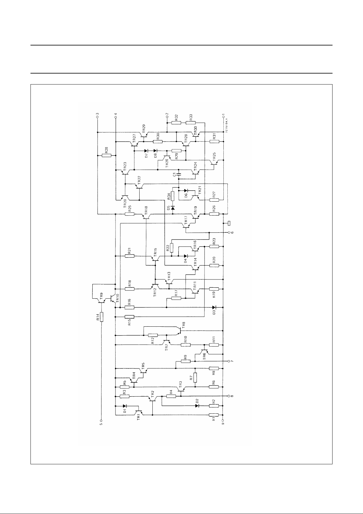
Fig.1 Circuit diagram.
Page 4
Philips Semiconductors Product specification
6 W audio power amplifier in car applications
TDA1010A
10 W audio power amplifier in mains-fed applications
RATINGS
Limiting values in accordance with the Absolute Maximum System (IEC 134)
Supply voltage V
Peak output current I
Repetitive peak output current I
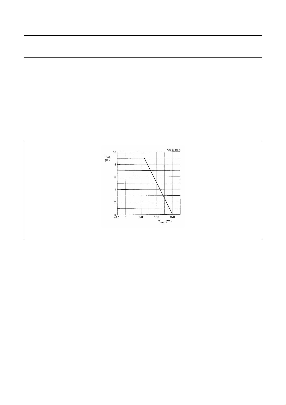
Total power dissipation see derating curve Fig.2
Storage temperature T
Operating ambient temperature T
A.C. short-circuit duration of load during sine-wave drive; without heatsink at
V
= 14,4 V
P
max. 24 V
P
max. 5 A
OM
max. 3 A
ORM
−55 to +150 °C
stg
−25 to +150 °C
amb
t
max. 100 hours
sc
Fig.2 Power derating curve.
HEATSINK DESIGN
Assume V
= 14,4 V; RL= 2 Ω; T
P
= 60 °C maximum; thermal shut-down starts at Tj= 150 °C. The maximum sine-wave
amb
dissipation in a 2 Ω load is about 5,2 W. The maximum dissipation for music drive will be about 75% of the worst-case
sine-wave dissipation, so this will be 3,9 W. Consequently, the total resistance from junction to ambient
R
= R
th j-aRth j-tab
Since R
R
th j-tab
= 23 − (10 + 1) = 12 K/W.
th h-a
++
= 10 K/W and R
th tab-hRth h-a
th tab-h
150 60–
---------------------39,
= 1 K/W,
23 K/W==
.
November 1982 4
Page 5

Philips Semiconductors Product specification
6 W audio power amplifier in car applications
TDA1010A
10 W audio power amplifier in mains-fed applications
D.C. CHARACTERISTICS
Supply voltage range V
Repetitive peak output current I
Total quiescent current at V
= 14,4 V I
P
P
ORM
tot
A.C. CHARACTERISTICS
T
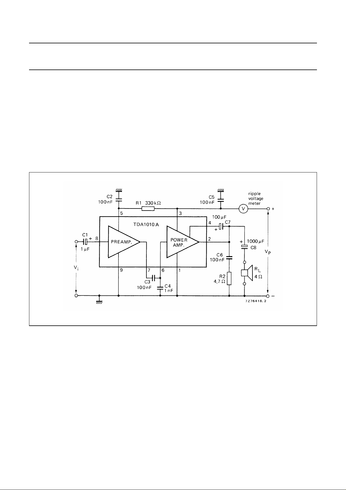
= 25 °C; VP= 14,4 V; RL= 4 Ω; f = 1 kHz unless otherwise specified; see also Fig.3.
amb
A.F. output power (see Fig.4) at d
= 10%;
tot
measured at pin 2; with bootstrap
V
= 14,4 V; RL= 2 Ω (note 1) P
P
V
= 14,4 V; RL= 4 Ω (note 1 and 2)
P
V
= 14,4 V; RL= 8 Ω (note 1) P
P
V
= 14,4 V; RL= 4 Ω; without bootstrap P
P
V
= 14,4 V; RL= 2Ω; with additional bootstrapresistor of 220Ωbetween pins 3 and 4 P
P
o
P
o
o
o
o
Voltage gain
preamplifier (note 3) G
power amplifier G
total amplifier G
Total harmonic distortion at Po= 1 W d
Efficiency at P
= 6 W η typ. 75 %
o
v1
v2
v tot
tot
Frequency response (−3 dB) B 80 Hz to 15 kHz
Input impedance
preamplifier (note 4) Z
typ. 30 kΩ
i
power amplifier (note 5) Zi typ. 20 kΩ
Output impedance of preamplifier; pin 7 (note 5) Zo typ. 20 kΩ
Output voltage preamplifier (r.m.s. value)
d
< 1% (pin 7) (note 3) V
tot
o(rms)
Noise output voltage (r.m.s. value; note 6)
R
= 0 Ω V
S
R
= 8,2 kΩ V
S
n(rms)
n(rms)
Ripple rejection at f = 1 kHz to 10 kHz (note 7) RR > 42 dB
at f = 100 Hz; C2 = 1 µF RR > 37 dB
Sensitivity for Po= 5,8 W V
Bootstrap current at onset of clipping; pin 4 (r.m.s. value) I
i
4(rms)
6 to 24 V
<3A
typ. 31 mA
typ. 6,4 W
> 5,9 W
typ. 6,2 W
typ. 3,4 W
typ. 5,7 W
typ. 9 W
typ. 24 dB
21 to 27 dB
typ. 30 dB
27 to 33 dB
typ. 54 dB
51 to 57 dB
typ. 0,2 %
20 to 40 kΩ
14 to 26 kΩ
14 to 26 kΩ
> 0,7 V
typ. 0,3 mV
typ. 0,7 mV
< 1,4 mV
typ. 10 mV
typ. 30 mA
November 1982 5
Page 6
Philips Semiconductors Product specification
6 W audio power amplifier in car applications
TDA1010A
10 W audio power amplifier in mains-fed applications
Notes
1. Measured with an ideal coupling capacitor to the speaker load.
2. Up to Po≤ 3 W : d
3. Measured with a load impedance of 20 kΩ.
4. Independent of load impedance of preamplifier.
5. Output impedance of preamplifier (ZΟ) is correlated (within 10%) with the input impedance (Zi) of the power
amplifier.
6. Unweighted r.m.s. noise voltage measured at a bandwidth of 60 Hz to 15 kHz (12 dB/octave).
7. Ripple rejection measured with a source impedance between 0 and 2 kΩ (maximum ripple amplitude: 2 V).
8. The tab must be electrically floating or connected to the substrate (pin 9).
tot
≤ 1%.
Fig.3 Test circuit.
November 1982 6
Page 7
Philips Semiconductors Product specification
6 W audio power amplifier in car applications
10 W audio power amplifier in mains-fed applications
TDA1010A
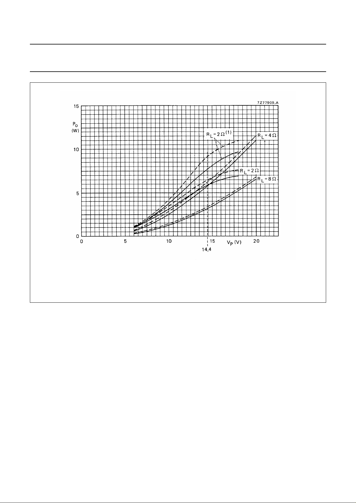
Fig.4 Output power of the circuit of Fig.3 as a function of the supply voltage with the load impedance as a
parameter; typical values. Solid lines indicate the power across the load, dashed lines that available at pin
2 of the TDA1010. RL= 2 Ω
pins 3 and 4. Measurements were made at f = 1 kHz, d
Fig. 5 See next page.
Total harmonic distortion in the circuit of Fig.3 as a function of the output power with the load impedance as a parameter;
typical values. Solid lines indicate the power across the load, dashed lines that available at pin 2 of the TDA1010.
RL= 2 Ω
made at f = 1 kHz, VP= 14,4 V.
(1)
has been measured with an additional 220 Ω bootstrap resistor between pins 3 and 4. Measurements were
(1)
has been measured with an additional 220 Ω bootstrap resistor between
= 10%, T
tot
amb
= 25 °C.
November 1982 7
Page 8

Philips Semiconductors Product specification
6 W audio power amplifier in car applications
10 W audio power amplifier in mains-fed applications
TDA1010A
Fig.5 For caption see preceding page.
Fig.6 Frequency characteristics of the circuit of Fig.3 for three values of load impedance; typical values.
Porelative to 0 dB = 1 W; VP= 14,4 V.
November 1982 8
Page 9

Philips Semiconductors Product specification
6 W audio power amplifier in car applications
10 W audio power amplifier in mains-fed applications
TDA1010A
Fig.7 Total power dissipation (solid lines) and the efficiency (dashed lines) of the circuit of Fig.3 as a function of
the output power with the load impedance as a parameter (for RL= 2 Ω an external bootstrap resistor of
220 Ω has been used); typical values. VP= 14,4 V; f = 1 kHz.
November 1982 9
Page 10

Philips Semiconductors Product specification
6 W audio power amplifier in car applications
10 W audio power amplifier in mains-fed applications
TDA1010A
Fig.8 Thermal resistance from heatsink to ambient of a 1,5 mm thick bright aluminium heatsink as a function of
the single-sided area of the heatsink with the total power dissipation as a parameter.
November 1982 10
Page 11

Philips Semiconductors Product specification
6 W audio power amplifier in car applications
10 W audio power amplifier in mains-fed applications
APPLICATION INFORMATION
TDA1010A
November 1982 11
Fig.9 Complete mono audio amplifier of a car radio.
Page 12

Philips Semiconductors Product specification
6 W audio power amplifier in car applications
10 W audio power amplifier in mains-fed applications
TDA1010A
Fig.10 Track side of printed-circuit board used for the circuit of Fig.9; p.c. board dimensions 92 mm × 52 mm.
Fig.11 Component side of printed-circuit board showing component layout used for the circuit of Fig.9.
November 1982 12
Page 13

Philips Semiconductors Product specification
6 W audio power amplifier in car applications
10 W audio power amplifier in mains-fed applications
TDA1010A
November 1982 13
Fig.12 Complete stereo car radio amplifier.
Page 14

Philips Semiconductors Product specification
6 W audio power amplifier in car applications
10 W audio power amplifier in mains-fed applications
TDA1010A
Fig.13 Track side of printed-circuit board used for the circuit of Fig.12; p.c. board dimensions 83 mm × 65 mm.
November 1982 14
Page 15

Philips Semiconductors Product specification
6 W audio power amplifier in car applications
10 W audio power amplifier in mains-fed applications
TDA1010A
Fig.14 Component side of printed-circuit board showing component layout used for the circuit of Fig.12.
Balance control is not on the p.c. board.
November 1982 15
Page 16

Philips Semiconductors Product specification
6 W audio power amplifier in car applications
10 W audio power amplifier in mains-fed applications
TDA1010A
Fig.15 Channel separation of the circuit of Fig.12 as a function of the frequency.
Fig.16 Power supply of circuit of Fig.17.
November 1982 16
Page 17

Philips Semiconductors Product specification
6 W audio power amplifier in car applications
10 W audio power amplifier in mains-fed applications
TDA1010A
November 1982 17
Fig.17 Complete mains-fed ceramic stereo pick-up amplifier; for power supply see Fig.16.
Page 18

Philips Semiconductors Product specification
6 W audio power amplifier in car applications
10 W audio power amplifier in mains-fed applications
TDA1010A
Fig.18 Track side of printed-circuit board used for the circuit of Fig.17 (Fig.16 partly); p.c. board dimensions
169 mm × 118 mm.
November 1982 18
Page 19

Philips Semiconductors Product specification
6 W audio power amplifier in car applications
10 W audio power amplifier in mains-fed applications
TDA1010A
Fig.19 Component side of printed-circuit board showing component layout used for the circuit of Fig.17
(Fig.16 partly).
November 1982 19
Page 20

Philips Semiconductors Product specification
6 W audio power amplifier in car applications
10 W audio power amplifier in mains-fed applications
TDA1010A
Fig.20 Channel separation of the circuit of Fig.18 as a function of frequency.
November 1982 20
Page 21

Philips Semiconductors Product specification
6 W audio power amplifier in car applications
10 W audio power amplifier in mains-fed applications
PACKAGE OUTLINE
SIL9MPF: plastic single in-line medium power package with fin; 9 leads
D
D
1
q
P
P
1
q
2
q
1
TDA1010A
SOT110-1
A
2
A
3
pin 1 index
seating plane
19
Z
b
DIMENSIONS (mm are the original dimensions)
A
A
18.5
17.8
max.
3.7
2
A
A
3
4
8.7
15.8
8.0
15.4
UNIT
mm
Note
1. Plastic or metal protrusions of 0.25 mm maximum per side are not included.
e
2
b
0.67
0.50
b
1
2
1.40
0.48
1.14
0.38
bcD
1.40
1.14
b
b
1
0 5 10 mm
scale
(1)
D
1
21.8
21.4
21.4
20.7
w M
(1)
E
eLPP
6.48
6.20
2.54
3.9
3.4
A
A
4
L
Q
q1q
q
Q
1
3.4
3.2
1.75
1.55
15.1
14.9
4.4
4.2
2.75
2.50
c
5.9
5.7
E
2
w
0.25
(1)
Z
max.
1.0
OUTLINE
VERSION
SOT110-1
IEC JEDEC EIAJ
REFERENCES
November 1982 21
EUROPEAN
PROJECTION
ISSUE DATE
92-11-17
95-02-25
Page 22

Philips Semiconductors Product specification
6 W audio power amplifier in car
applications
TDA1010A
SOLDERING
Introduction
There is no soldering method that is ideal for all IC
packages. Wave soldering is often preferred when
through-hole and surface mounted components are mixed
on one printed-circuit board. However, wave soldering is
not always suitable for surface mounted ICs, or for
printed-circuits with high population densities. In these
situations reflow soldering is often used.
This text gives a very brief insight to a complex technology.
A more in-depth account of soldering ICs can be found in
“IC Package Databook”
our
Soldering by dipping or by wave
The maximum permissible temperature of the solder is
260 °C; solder at this temperature must not be in contact
with the joint for more than 5 seconds. The total contact
time of successive solder waves must not exceed
5 seconds.
DEFINITIONS
Data sheet status
Objective specification This data sheet contains target or goal specifications for product development.
Preliminary specification This data sheet contains preliminary data; supplementary data may be published later.
Product specification This data sheet contains final product specifications.
(order code 9398 652 90011).
The device may be mounted up to the seating plane, but
the temperature of the plastic body must not exceed the
specified maximum storage temperature (T
printed-circuit board has been pre-heated, forced cooling
may be necessary immediately after soldering to keep the
temperature within the permissible limit.
Repairing soldered joints
Apply a low voltage soldering iron (less than 24 V) to the
lead(s) of the package, below the seating plane or not
more than 2 mm above it. If the temperature of the
soldering iron bit is less than 300 °C it may remain in
contact for up to 10 seconds. If the bit temperature is
between 300 and 400 °C, contact may be up to 5 seconds.
stg max
). If the
Limiting values
Limiting values given are in accordance with the Absolute Maximum Rating System (IEC 134). Stress above one or
more of the limiting values may cause permanent damage to the device. These are stress ratings only and operation
of the device at these or at any other conditions above those given in the Characteristics sections of the specification
is not implied. Exposure to limiting values for extended periods may affect device reliability.
Application information
Where application information is given, it is advisory and does not form part of the specification.
LIFE SUPPORT APPLICATIONS
These products are not designed for use in life support appliances, devices, or systems where malfunction of these
products can reasonably be expected to result in personal injury. Philips customers using or selling these products for
use in such applications do so at their own risk and agree to fully indemnify Philips for any damages resulting from such
improper use or sale.
November 1982 22
 Loading...