

Page 1

INTEGRATED CIRCUITS
DATA SH EET
TDA1001B
TDA1001BT
Interference and noise suppression
circuit for FM receivers
Product specification
File under Integrated Circuits, IC01
December 1982
Page 2

Philips Semiconductors Product specification
Interference and noise suppression
circuit for FM receivers
TDA1001B
TDA1001BT
GENERAL DESCRIPTION
The TDA1001B is a monolithic integrated circuit for suppressing interference and noise in FM mono and stereo receivers.
Features
• Active low-pass and high-pass filters
• Interference pulse detector with adjustable and controllable response sensitivity
• Noise detector designed for FM i.f. amplifiers with ratio detectors or quadrature detectors
• Schmitt trigger for generating an interference suppression pulse
• Active pilot tone generation (19 kHz)
• Internal voltage stabilization
QUICK REFERENCE DATA
Supply voltage (pin 9) V
Supply current (pin 9) I
P
P
typ. 12 V
typ. 14 mA
A.F. input signal handling (pin 1)
(peak-to-peak value) V
Input resistance (pin 1) R
Voltage gain (V
1-16/V6-16
)G
i(p-p)
i
v
typ. 1 V
min. 35 kΩ
typ. 0,5 dB
Total harmonic distortion THD typ. 0,25 %
Bandwidth B typ. 70 kHz
Suppression pulse threshold voltage
(peak value); R
= 0 V
13
Suppression pulse duration t
Supply voltage range (pin 9) V
Operating ambient temperature range T
i(tr)OM
s
P
amb
typ. 19 mV
typ. 27 µs
7,5 to 16 V
−30 to + 80 °C
PACKAGE OUTLINE
TDA1001B: 16-lead DIL; plastic (SOT38); SOT38-1; 1996 September 06.
TDA1001BT: 16-lead mini-pack; plastic (SO16; SOT109A); SOT116-1; 1996 September 06.
December 1982 2
Page 3
Philips Semiconductors Product specification
Interference and noise suppression circuit
for FM receivers
TDA1001B
TDA1001BT
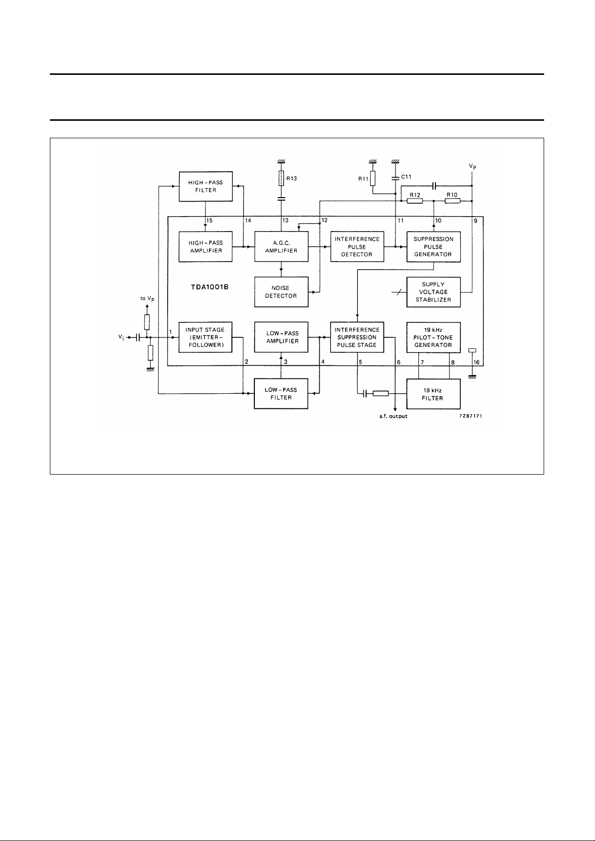
Fig.1 Block diagram.
December 1982 3
Page 4
Philips Semiconductors Product specification
Interference and noise suppression circuit
for FM receivers
TDA1001B
TDA1001BT
RATINGS
Limiting values in accordance with the Absolute Maximum System (IEC 134)
Supply voltage (pin 9) V
Input voltage (pin 1) V
Output current (pin 6) I
P
1-16
6
−I
6
max. 18 V
max. V
P
max. 1 mA
max. 15 mA
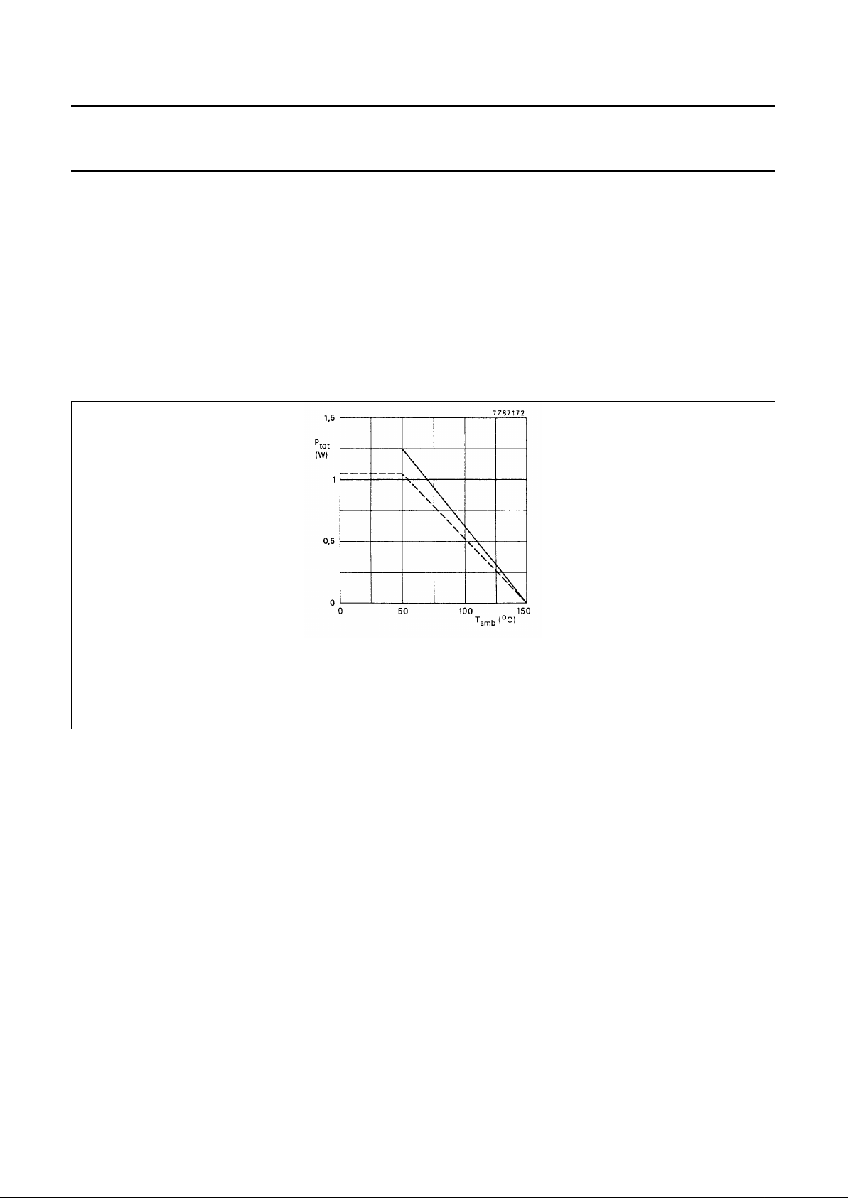
Total power dissipation see derating curves Fig.2
Storage temperature range T
Operating ambient temperature range T
stg
amb
−65 to +150 °C
−30 to +80 °C
V
in plastic DIL (SOT-38) package (TDA1001B).
− − − − − − in plastic mini-pack (SO-16; SOT-109A) package (TDA1001BT); mounted on a ceramic substrate of 50×15 ×0,7 mm.
Fig.2 Power derating curves.
December 1982 4
Page 5

Philips Semiconductors Product specification
Interference and noise suppression circuit
for FM receivers
CHARACTERISTICS
= 12 V; T
V
P
Input stage
Input impedance (pin 1)
f = 40 kHz Z
Input resistance (pin 1)
with pin 2 not connected R
Input bias current (pin 1)
= 4,8 V I
V
1-16
Output resistance (pin 2)
unloaded R
Internal emitter resistance R
Low-pass amplifier
Input resistance (pin 3) R
Input bias current (pin 3) I
Output resistance (pin 4) R
Voltage gain (V
Suppression pulse stage
Input offset current at pin 5
during the suppression time t
Output stage
Output resistance (pin 6) R
Internal emitter resistance R
Current gain (I
Pilot tone generation (19 kHz)
Input impedance (pin 8) Z
Output impedance (pin 7)
pin 8 open Z
Output bias current (pin 7) I
Current gain (I
High-pass amplifier
Input resistance (pin 15) R
Input bias current (pin 15) I
Output resistance (pin 14) R
Voltage gain (V
= 25 °C; measured in Fig.4; unless otherwise specified
amb
PARAMETER SYMBOL MIN. TYP. MAX. UNIT
i1
i1
o2
2-16
i3
i3
o4
)G
4/V3
S
)G
5/I6
)G
7/I8
)G
14/15
I
io5
o7
i15
v4/3
o6
6-16
i5/6
i7/8
i15
o14
v14/15
TDA1001B
TDA1001BT
−45 − kΩ
i1
− 600 − kΩ
− 615µA
low-ohmic
− 5,6 − kΩ
10 −−MΩ
−−7µA
−−5Ω
− 1,1 −
− 50 200 nA
low-ohmic
− 6 − kΩ
− 85 − dB
−−1Ω
i8
150 −−kΩ
o7
0,7 1 1,3 mA
− 3 −
10 −−MΩ
−−7µA
−−5Ω
− 1,4 −
December 1982 5
Page 6

Philips Semiconductors Product specification
Interference and noise suppression circuit
for FM receivers
PARAMETER SYMBOL MIN. TYP. MAX. UNIT
A.G.C. amplifier; interference and noise detectors
Internal resistance (pins 13 and 14) R
Operational threshold voltage
(uncontrolled); peak value (pin 14)
of the interference pulse detector ± V
of the noise detector ± V
Output voltage (peak value; pin 11) V
Output control current (pin 12)
(peak value) I
Output bias current (pin 12) I
Input threshold voltage for onset of control (pin 12) V
(V
+ 3 dB) or: − 0,66V
i(tr)O
Suppression pulse generation (Schmitt trigger)
Switching threshold (pin 11)
1: gate disabled V
2: gate enabled V
Switching hysteresis ∆V
Input offset current (pin 11) I
Output current (pin 10)
gate disabled; peak value I
Reverse output current (pin 10) I
Sensitivity (pin 10) V
13-14
14int m
14n m
11-16M
12M
o12
12-9
11-16
11-16
11-16
io11
o10M
R10
10-16
TDA1001B
TDA1001BT
1,5 2,0 2,5 kΩ
− 15 − mV
− 6,5 − mV
5,2 5,8 6,4 V
150 200 250 µA
− 2,5 6 µA
360 425 500 mV
− mV
BE
− 3,2 − V
− 2,0 − V
− 1,2 − V
−−100 nA
0,6 1 1,4 mA
−−2µA
2,5 −−V
December 1982 6
Page 7

Philips Semiconductors Product specification
Interference and noise suppression circuit
for FM receivers
APPLICATION INFORMATION
= 12 V; T
V
P
Supply voltage range (pin 9) V
Quiescent supply current (pin 9) I
Signal path
D.C. input voltage (pin 1) V
Input impedance (pin 1); f = 40 kHz |Z
D.C. output voltage (pin 6) V
Output resistance (pin 6) R
Voltage gain (V
−3 dB point of low-pass filter f
Sensitivity for THD < 0,5%
(peak-to-peak value) V
Residual interference pulse after suppression
(see Fig.3); pin 7 to ground;
V
i(tr)M
Interference suppression at R13 = 0;
notes 5 and 6; V
(sinewave); V
Interference processing
Input signal at pin 1; output signal at pin 10
Suppression pulse threshold voltage; control
function OFF (pin 9 connected to pin 12);
r.m.s. value; note 1
measured with sinewave input signal
f = 120 kHz; −V
at R13 = 0 Ω V
at R13 = 2,7 kΩ V
voltage difference for safe triggering/
non-triggering (r.m.s. value) ∆V
measured with interference pulses
f = 400 Hz (see Fig.3); peak value
at R13 = 0 Ω V
at R13 = 2,7 kΩ V
Suppression pulse duration (note 2) t
= 25 °C; f = 1 kHz; measured in Fig.4; unless otherwise specified
amb
PARAMETER SYMBOL MIN. TYP. MAX. UNIT
P
P
1-16
6-16
)G
6/V1
(−3dB)
i(p-p)
= 100mV; (peak-to-peak value) V
= 30 mV; f = 19 kHz
i(rms)
= 60 mV; fr= 400 Hz α
i(tr)M
> 1 V
10-9
6-16(p-p)
int
i(tr)rms
i(tr)rms
i(tr)M
i(tr)M
S
TDA1001B
TDA1001BT
7,5 12 16 V
10 14 18 mA
− 4,5 − V
|35−−kΩ
i1
2,4 2,8 − V
o6
v6/1
i(rms)
0 0,5 1 dB
− 70 − kHz
1,2 1,8 − V
−−3mV
20 30 − dB
81114mV
18 28,5 40 mV
− 1 − mV
− 19 − mV
− 45 − mV
24 27 30 µs
low-ohmic
December 1982 7
Page 8

Philips Semiconductors Product specification
Interference and noise suppression circuit
for FM receivers
TDA1001B
TDA1001BT
PARAMETER SYMBOL MIN. TYP. MAX. UNIT
Noise threshold feedback control (notes 1 and 3)
Noise input voltage (r.m.s. value) f = 120 kHz
sinewave for V
at R13 = 0 Ω V
at R13 = 2,7 kΩ V
for V
= 425 mV (V
12-9
at R13 = 0 Ω V
at R13 = 2,7 kΩ V
for V
= 560 mV (V
12-9
at R13 = 0 Ω V
at R13 = 2,7 kΩ V
= 300 mV
12-9
i(tr)O
i(tr)O
+ 3 dB)
+ 20 dB)
ni(rms)
ni(rms)
ni(rms)
ni(rms)
ni(rms)
ni(rms)
2,3 3,3 4,3 mV
− 8,2 − mV
− 7,3 − mV
− 16,5 − mV
33 45 57 mV
− 107 − mV
Amplification control voltage by interference intensity
(note 4)
= 50 mV; f = 19 kHz;
V
i(rms)
= 300 mV; r.m.s. value
V
i(tr)M
at repetition frequency f
at repetition frequency f
= 1 kHz V
r
= 16 kHz V
r
o6(rms)
o6(rms)
49 − 56 mV
45 − 65 mV
Notes to application information
1. The interference suppression and noise feedback control thresholds can be determined by R13 or a capacitive
voltage divider at the input of the high-pass filter and they are defined by the following formulae:
V
= (1 + R13/RS) × V
i(tr)
Vni = (1 + R13/RS) × V
in which RS= 2 kΩ;
i(tr)O
in which RS= 2 kΩ.
niO
2. The suppression pulse duration is determined by C11 = 2,2 nF and R11 = 6,8 kΩ.
3. The characteristic of the noise feedback control is determined by R12 (and R10).
4. The feedback control of the interference suppression threshold at higher repetition frequencies is determined by R10
(and R12).
5. The 19 kHz generator can be adjusted with R
7-16
(and R
). Adjustment is not required if components with small
7-8
tolerances are used e.g. ∆R < 1% and ∆C < 2%.
6. Measuring conditions:
The peak output noise voltage (V
µs (R = 5 kΩ, C = 10 nF); the reference value of 0 dB is V
, CCITT filter) shall be measured at the output with a de-emphazing time T = 50
no m
with the 19 kHz generator short-circuited (pin 7
o int
grounded).
December 1982 8
Page 9

Philips Semiconductors Product specification
Interference and noise suppression circuit
for FM receivers
Fig.3 Measuring signal for interference suppression; at the input (pin 1) a square-wave is applied with a duration
of ttr = 10 µs and with rise and fall times tr = tf = 10 ns.
TDA1001B
TDA1001BT
Fig.4 Application circuit diagram.
December 1982 9
Page 10

Philips Semiconductors Product specification
Interference and noise suppression circuit
for FM receivers
PACKAGE OUTLINES
DIP16: plastic dual in-line package; 16 leads (300 mil); long body
D
seating plane
L
Z
16
e
b
b
1
9
A
1
w M
TDA1001B
TDA1001BT
SOT38-1
M
E
A
2
A
c
(e )
1
M
H
pin 1 index
1
0 5 10 mm
DIMENSIONS (inch dimensions are derived from the original mm dimensions)
A
UNIT
mm
inches
Note
1. Plastic or metal protrusions of 0.25 mm maximum per side are not included.
A
max.
4.7 0.51 3.7
OUTLINE
VERSION
SOT38-1
min.
A
1 2
max.
0.15
IEC JEDEC EIAJ
050G09 MO-001AE
b
1.40
1.14
0.055
0.045
b
0.53
0.38
0.021
0.015
1
cEe M
0.32
0.23
0.013
0.009
REFERENCES
D
21.8
21.4
0.86
0.84
8
scale
(1) (1)
6.48
6.20
0.26
0.24
E
(1)
Z
e
0.30
1
0.15
0.13
M
L
3.9
3.4
E
8.25
7.80
0.32
0.31
EUROPEAN
PROJECTION
9.5
8.3
0.37
0.33
w
H
0.2542.54 7.62
0.010.100.0200.19
ISSUE DATE
92-10-02
95-01-19
max.
2.2
0.087
December 1982 10
Page 11

Philips Semiconductors Product specification
Interference and noise suppression circuit
for FM receivers
SO16: plastic small outline package; 16 leads; body width 3.9 mm
D
c
y
Z
16
9
TDA1001B
TDA1001BT
SOT109-1
E
H
E
A
X
v M
A
pin 1 index
1
e
0 2.5 5 mm
DIMENSIONS (inch dimensions are derived from the original mm dimensions)
mm
A
max.
1.75
0.069
A1A2A
0.25
1.45
0.10
1.25
0.0098
0.057
0.0039
0.049
0.25
0.01
b
3
p
0.49
0.25
0.36
0.19
0.0098
0.019
0.0075
0.014
UNIT
inches
Note
1. Plastic or metal protrusions of 0.15 mm maximum per side are not included.
(1)E(1) (1)
cD
10.0
9.8
0.39
0.38
8
b
p
scale
eHELLpQZywv θ
4.0
1.27
3.8
0.16
0.050
0.15
w M
6.2
5.8
0.24
0.23
A
2
1.05
0.041
Q
A
1
detail X
1.0
0.7
0.4
0.6
0.028
0.039
0.020
0.016
(A )
L
p
L
0.25 0.1
0.25
0.01
0.01 0.004
A
3
θ
0.7
0.3
0.028
0.012
o
8
o
0
OUTLINE
VERSION
SOT109-1
IEC JEDEC EIAJ
076E07S MS-012AC
REFERENCES
December 1982 11
EUROPEAN
PROJECTION
ISSUE DATE
91-08-13
95-01-23
Page 12

Philips Semiconductors Product specification
Interference and noise suppression circuit
for FM receivers
SOLDERING
Introduction
There is no soldering method that is ideal for all IC
packages. Wave soldering is often preferred when
through-hole and surface mounted components are mixed
on one printed-circuit board. However, wave soldering is
not always suitable for surface mounted ICs, or for
printed-circuits with high population densities. In these
situations reflow soldering is often used.
This text gives a very brief insight to a complex technology.
A more in-depth account of soldering ICs can be found in
“IC Package Databook”
our
DIP
OLDERING BY DIPPING OR BY WA VE
S
The maximum permissible temperature of the solder is
260 °C; solder at this temperature must not be in contact
with the joint for more than 5 seconds. The total contact
time of successive solder waves must not exceed
5 seconds.
The device may be mounted up to the seating plane, but
the temperature of the plastic body must not exceed the
specified maximum storage temperature (T
printed-circuit board has been pre-heated, forced cooling
may be necessary immediately after soldering to keep the
temperature within the permissible limit.
R
EPAIRING SOLDERED JOINTS
Apply a low voltage soldering iron (less than 24 V) to the
lead(s) of the package, below the seating plane or not
more than 2 mm above it. If the temperature of the
soldering iron bit is less than 300 °C it may remain in
contact for up to 10 seconds. If the bit temperature is
between 300 and 400 °C, contact may be up to 5 seconds.
SO
REFLOW SOLDERING
Reflow soldering techniques are suitable for all SO
packages.
(order code 9398 652 90011).
). If the
stg max
TDA1001B
TDA1001BT
Several techniques exist for reflowing; for example,
thermal conduction by heated belt. Dwell times vary
between 50 and 300 seconds depending on heating
method. Typical reflow temperatures range from
215 to 250 °C.
Preheating is necessary to dry the paste and evaporate
the binding agent. Preheating duration: 45 minutes at
45 °C.
AVE SOLDERING
W
Wave soldering techniques can be used for all SO
packages if the following conditions are observed:
• A double-wave (a turbulent wave with high upward
pressure followed by a smooth laminar wave) soldering
technique should be used.
• The longitudinal axis of the package footprint must be
parallel to the solder flow.
• The package footprint must incorporate solder thieves at
the downstream end.
During placement and before soldering, the package must
be fixed with a droplet of adhesive. The adhesive can be
applied by screen printing, pin transfer or syringe
dispensing. The package can be soldered after the
adhesive is cured.
Maximum permissible solder temperature is 260 °C, and
maximum duration of package immersion in solder is
10 seconds, if cooled to less than 150 °C within
6 seconds. Typical dwell time is 4 seconds at 250 °C.
A mildly-activated flux will eliminate the need for removal
of corrosive residues in most applications.
EPAIRING SOLDERED JOINTS
R
Fix the component by first soldering two diagonally-
opposite end leads. Use only a low voltage soldering iron
(less than 24 V) applied to the flat part of the lead. Contact
time must be limited to 10 seconds at up to 300 °C. When
using a dedicated tool, all other leads can be soldered in
one operation within 2 to 5 seconds between
270 and 320 °C.
Reflow soldering requires solder paste (a suspension of
fine solder particles, flux and binding agent) to be applied
to the printed-circuit board by screen printing, stencilling or
pressure-syringe dispensing before package placement.
December 1982 12
Page 13

Philips Semiconductors Product specification
Interference and noise suppression circuit
for FM receivers
DEFINITIONS
Data sheet status
Objective specification This data sheet contains target or goal specifications for product development.
Preliminary specification This data sheet contains preliminary data; supplementary data may be published later.
Product specification This data sheet contains final product specifications.
Limiting values
Limiting values given are in accordance with the Absolute Maximum Rating System (IEC 134). Stress above one or
more of the limiting values may cause permanent damage to the device. These are stress ratings only and operation
of the device at these or at any other conditions above those given in the Characteristics sections of the specification
is not implied. Exposure to limiting values for extended periods may affect device reliability.
Application information
Where application information is given, it is advisory and does not form part of the specification.
LIFE SUPPORT APPLICATIONS
These products are not designed for use in life support appliances, devices, or systems where malfunction of these
products can reasonably be expected to result in personal injury. Philips customers using or selling these products for
use in such applications do so at their own risk and agree to fully indemnify Philips for any damages resulting from such
improper use or sale.
TDA1001B
TDA1001BT
December 1982 13
 Loading...