

Page 1
STW10NB60
N - CHANNEL 600V - 0.69Ω - 10A - TO-247
PowerMESH MOSFET
TYPE V
DSS
R
DS(on)
I
D
ST W 10NB60 600 V < 0. 8 Ω 10 A
■ TYPICALR
■ EXTREMELYHIGH dv/dtCAPABILITY
■ 100%AVALANCHETESTED
■ VERYLOW INTRINSIC CAPACITANCES
■ GATECHARGE MINIMIZED
DS(on)
= 0.69 Ω
DESCRIPTION
Using the latest high voltage MESH OVERLAY
process, STMicroelectronics has designed an
advanced family of power MOSFETs with
outstanding performances. The new patent
pending strip layout coupled with the Company’s
proprietary edge termination structure, gives the
lowest R
per area, exceptional avalanche
DS(on)
and dv/dt capabilities and unrivalled gate charge
and switching characteristics.
APPLICATIONS
■ SWITCHMODE POWER SUPPLIES (SMPS)
■ DC-AC CONVERTERS FOR WELDING
EQUIPMENTANDUNINTERRUPTIBLE
POWERSUPPLIESAND MOTOR DRIVE
■ HIGHCURRENT, HIGH SPEED SWITCHING
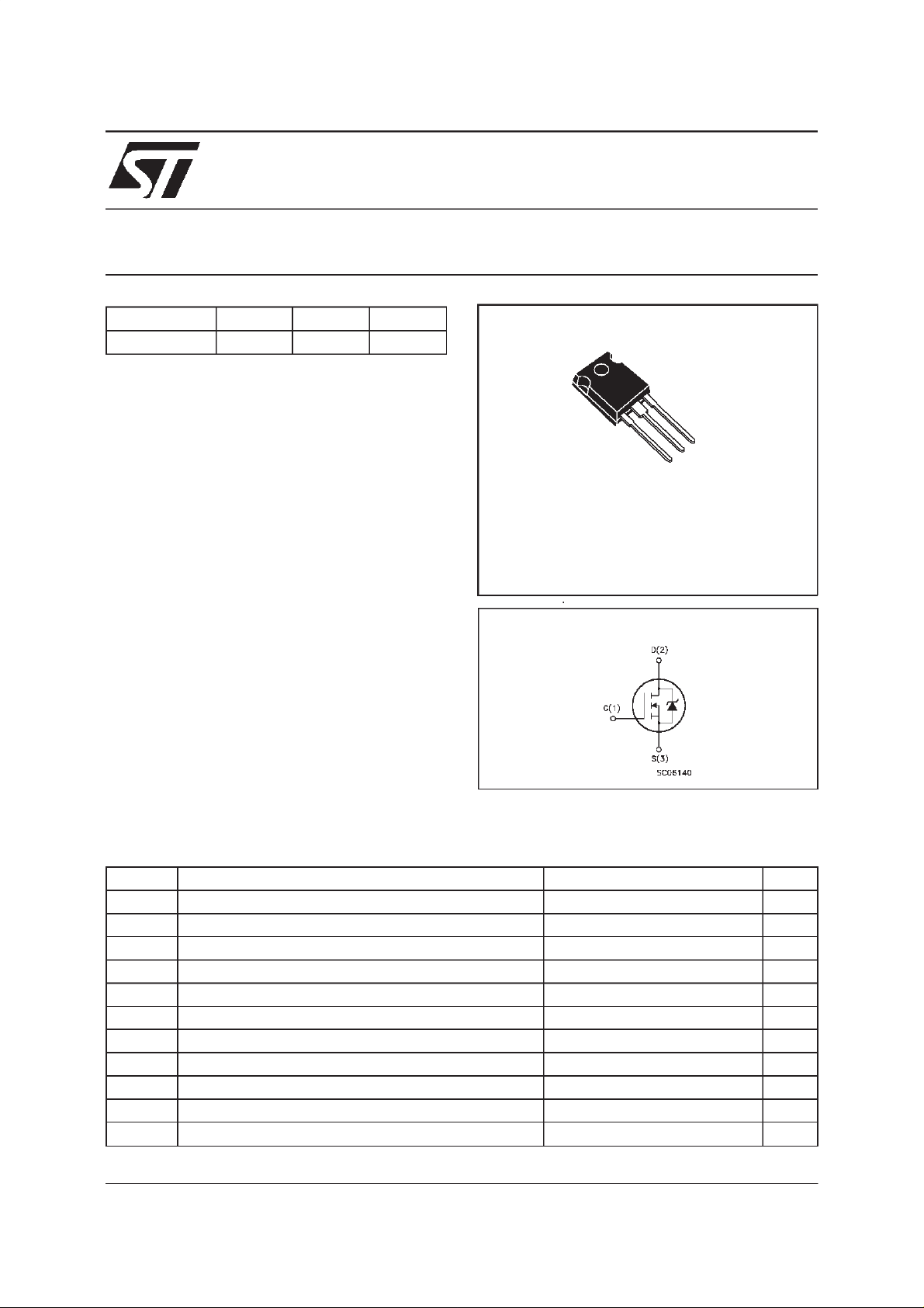
3
2
1
TO-247
INTERNAL SCHEMATIC DIAGRAM
ABSOLUTE MAXIMUM RATINGS
Symbol Parameter Value Unit
V
V
V
I
DM
P
dv/dt(
T
(•) Pulsewidth limited by safe operating area (1)ISD≤10A, di/dt ≤ 200 A/µs, VDD≤ V
October 1998
Dra in- sour c e Voltage ( VGS= 0) 600 V
DS
Dra in- gate Vol t age (RGS=20kΩ) 600 V
DGR
Gat e-source Voltage
GS
I
Dra in Curr ent (c ont inuous) at Tc=25oC10A
D
I
Dra in Curr ent (c ont inuous) at Tc=100oC6.2A
D
30 V
±
(•) Dra in Curr ent (p ulsed) 40 A
Tot al Dissipat ion at Tc=25oC 160 W
tot
Der ati ng Factor 1.28 W/
1) P eak Diode Recover y voltage slope 4.5 V/ns
St orage Tem pe rat ure -65 to 150
stg
T
Max. Oper at ing Junction Tem perature 150
j
,Tj≤T
(BR)DSS
JMAX
o
C
o
C
o
C
1/8
Page 2
STW10NB60
THERMAL DATA
R
thj-case
Rthj-amb
R
thc-sink
T
AVALANCHE CHARACTERISTICS
Symbol Parameter Max Value Unit
I
AR
E
Ther mal Res istance J unction- cas e Max
Ther mal Res istance J unction- ambient Max
Ther mal Res istance C ase - sink Ty p
Maximum Lead T emperat ur e For S o lder ing Purpose
l
Avalanche Current, Repetitive or Not-Repetitive
(pulse width limited by T
Single Pulse A valanche E ner gy
AS
(starting T
=25oC, ID=IAR,VDD=50V)
j
max,δ <1%)
j
0.78
30
0.1
300
10 A
850 mJ
o
C/W
oC/W
o
C/W
o
C
ELECTRICAL CHARACTERISTICS
=25oC unless otherwisespecified)
(T
case
OFF
Symbol Parameter Test Conditions Min. Typ. Max. Unit
V
(BR)DSS
Drain-source
ID=250µAVGS= 0 600 V
Break dow n Volt age
I
DSS
I
GSS
Zero Gate Voltage
Drain Current (V
GS
Gat e- bod y Leakage
Current (V
DS
=0)
=0)
V
=MaxRating
DS
=MaxRating Tc=100oC
V
DS
V
=± 30 V
GS
1
50
100 nA
±
ON(∗)
Symbol Parameter Test Conditions Min. Typ. Max. Unit
V
GS(th)
R
DS(on)
Gate Threshold Voltage VDS=VGSID= 250 µA 345V
Sta t ic Dr ain -s ource O n
VGS=10V ID=4 A 0.69 0.8
Resistance
I
D(on)
On State Drain Current VDS>I
D(on)xRDS(on)max
10 A
VGS=10V
DYNAMIC
Symbol Parameter Test Conditions Min. Typ. Max. Unit
g
(∗)Forward
fs
Tr ansc on duc tance
C
C
C
Input C apac i t ance
iss
Out put Capacitance
oss
Reverse T r ansfer
rss
Capacit a nc e
VDS>I
D(on)xRDS(on)maxID
=17A 3 6.5 S
VDS=25V f=1MHz VGS= 0 1480
210
25
1924
273
33
µ
µA
Ω
pF
pF
pF
A
2/8
Page 3
STW10NB60
ELECTRICAL CHARACTERISTICS
(continued)
SWITCHING ON
Symbol Parameter Test Conditions Min. Typ. Max. Unit
t
d(on)
t
r
Turn-on Time
Rise T i me
VDD=300V ID= 4.5 A
R
=4.7
G
Ω
VGS=10V
25
11
35
15
(see test circuit, figure 3)
Q
Q
Q
Tot al G at e Char ge
g
Gat e- Source Char g e
gs
Gate-Drain Charge
gd
VDD= 480 V ID=9 A VGS=10V
R
=4.7
G
Ω
VGS=10V
40
10.5
17.5
56 nC
SWITCHING OFF
Symbol Parameter Test Conditions Min. Typ. Max. Unit
t
r(Voff)
t
t
Off-voltage Rise T im e
Fall T ime
f
Cross-over Time
c
VDD=480V ID=9A
=4.7 Ω VGS=10V
R
G
(see test circuit, figure 5)
12
10
21
17
14
29
SOURCEDRAINDIODE
Symbol Parameter Test Conditions Min. Typ. Max. Unit
I
SD
I
SDM
V
SD
t
Q
I
RRM
(∗) Pulsed: Pulse duration = 300µs, duty cycle 1.5 %
(•) Pulse width limited by safe operating area
Source-drain Current
(•)
Source-drain Current
10
40
(pulsed)
(∗)ForwardOnVoltage ISD=10A VGS=0 1.6 V
Reverse Re covery
rr
Time
Reverse Re covery
rr
ISD=9A di/dt=100A/µs
= 100 V Tj=150oC
V
DD
(see test circuit, figure 5)
600
5.4
Charge
Reverse Re covery
18
Current
ns
ns
nC
nC
ns
ns
ns
A
A
ns
µ
A
C
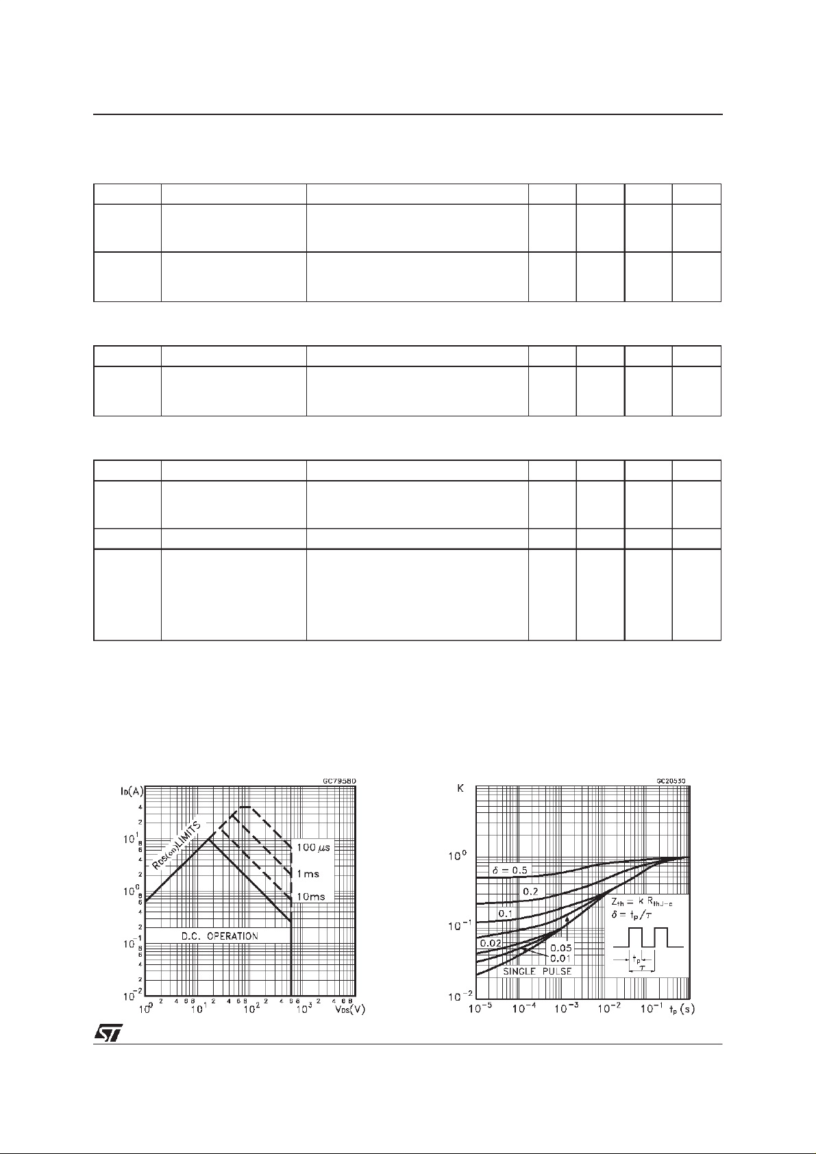
SafeOperating Area ThermalImpedance
3/8
Page 4

STW10NB60
OutputCharacteristics
Transconductance
TransferCharacteristics
Static Drain-sourceOn Resistance
Gate Charge vs Gate-sourceVoltage
4/8
CapacitanceVariations
Page 5

STW10NB60
NormalizedGate ThresholdVoltage vs
Temperature
Source-drainDiode Forward Characteristics
NormalizedOn Resistancevs Temperature
5/8
Page 6

STW10NB60
Fig. 1:
UnclampedInductiveLoad TestCircuit
Fig. 3: Switching Times Test CircuitsFor
ResistiveLoad
Fig. 2:
UnclampedInductive Waveform
Fig. 4: Gate Charge test Circuit
Fig. 5:
Test CircuitFor InductiveLoad Switching
And Diode Recovery Times
6/8
Page 7

TO-247 MECHANICAL DATA
STW10NB60
DIM.
MIN. TYP. MAX. MIN. TYP. MAX.
A 4.7 5.3 0.185 0.209
D 2.2 2.6 0.087 0.102
E 0.4 0.8 0.016 0.031
F 1 1.4 0.039 0.055
F3 2 2.4 0.079 0.094
F4 3 3.4 0.118 0.134
G 10.9 0.429
H 15.3 15.9 0.602 0.626
L 19.7 20.3 0.776 0.779
L3 14.2 14.8 0.559 0.413 0.582
L4 34.6 1.362
L5 5.5 0.217
M 2 3 0.079 0.118
Dia 3.55 3.65 0.140 0.144
mm inch
P025P
7/8
Page 8

STW10NB60
Information furnished is believed to beaccurate and reliable. However, STMicroelectronics assumes no responsibility for the consequences
of use of such information nor for any infringement of patents or other rights of third parties which may result from its use. No license is
granted by implication or otherwise under any patent or patent rights of STMicroelectronics. Specification mentioned in thispublication are
subject to change without notice. This publication supersedes and replaces all information previously supplied. STMicroelectronics products
are not authorized for use as critical components in life support devices or systems without express written approval of STMicroelectronics.
The ST logo is a trademarkof STMicroelectronics
1998 STMicroelectronics – Printed in Italy – All Rights Reserved
STMicroelectronics GROUP OF COMPANIES
Australia - Brazil - Canada - China -France - Germany - Italy - Japan - Korea - Malaysia - Malta - Mexico - Morocco - The Netherlands -
Singapore - Spain - Sweden - Switzerland - Taiwan - Thailand - UnitedKingdom - U.S.A.
http://www.st.com
.
8/8
 Loading...