

Page 1
STV9432TA
100MHz OSD FOR MONITOR
INCLUDING BEAM CURRENTS & VIDEO TIMING ANALYZER
• MULTIFUNCTION OSD FOR MONITOR
• INCLUDES FACILITIES FOR CUT-OFF VOLTAGES MONITORING:
- THREE 8 BITS ADC INPUTS
- ADC TRIGGER DURING RETRACE TIME OF A
PROGRAMMED LINE
• INCLUDES FACILITIES FOR SCREEN SIZE &
CENTERING AUTO SETUP
- HS, VS, VIDEO TIMING MEASUREMENTS
• 100MHz MAX. PIXEL CLOCK, AVAILABLE FOR
ANY LINE FREQUENCY BETWEEN 15 AND
140 kHz
• 12 x 18 CHARACTER ROM FONT INCLUDES:
- 240 MONOCOLO R CHARAC TER S
- 16 MULTICOLOR CHARACTERS
• CHARACTER FLASHING
• UP TO 1K CHARACTERS TEXT DISPLAY
• ULTRA HIGH FREQUENCY PLL FOR JITTERFREE DISPLAY
• FLEXIBLE DISPLAY:
- ANY CHARACTER WIDTH AND HEI GHT
- ANYWHERE IN THE SCREEN
• SINGLE BYTE CHARACTER CODES AND
COLOR LOOK-UP TABLE FOR EASY PROGRAMMING AND FAST ACCESS
• CHARACTER FLIP OPERATIONS
• WIDE DISPLAY WINDOW ALLOWS PATTERN
GENERATION FOR FACTORY ADJUSTMENTS
2
•I
C BUS MCU INTERFACE
DESCRIPTION
Connected to a host MCU via a serial I2C Bus, the
STV9432 TA is a multifunction s lav e peripheral dev ic e
integrating the following blocks:
- On-screen Display. It includes a MASK PROGRAMMABLE ROM that holds the CUSTOM
CHARACTER FONT, a 1Kbytes RAM that stores
the code strings of the different lines of text to be
displayed, and a set of registers to program character sizes and colors. A built-in digital PLL, oper-
ating at very high frequency, provides an accurate
display without visible jitter for a wide line frequency range from 15 to 140 kHz.
- Cut-off Monitoring Circuitry includes 3 x 8 bits
ADCs and a programmable ADC sampling trigger.
It gives the possibility to measure the three beam
currents, during the horizontal flyback, at a given
line in the frame, provided that the three ADC
inputs are connected to a beam current sensing
circuitry. The values are stored in three BEAM
CURRENT REGISTERS, and available for MCU
read.
- Video Timing Analyzer. Using the Horizontal Sync,
Vertical Sync, Horizontal Flyback, and "Video
Active" inputs, a set of counters provide the different timing measurements necessary to analyze
the current Video timing characteristics to make
the automatic set-up of screen size and centering.
The measurements are initialized on the same
programmable trigger line than in the above cut-off
monitoring circuitry
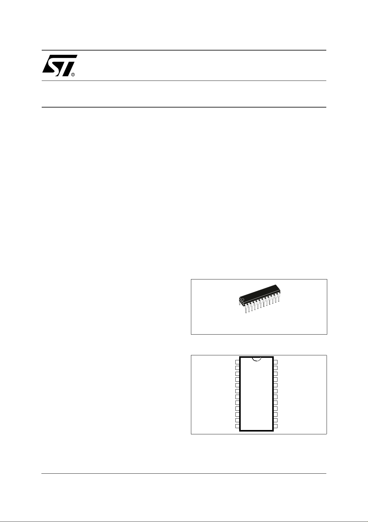
SDIP24 (Plastic Package)
ORDER CODE: STV9432TA
PIN CO NNECTIONS
24
1
2
3
SDA
4
SCL
5
HS
6
VS
HFLY
7
AV
8
DV
9
DD
10
DV
SS
11
XTI
12
XTO OV
23
2221RCI
20
19
18
17
16
15
14
13
TESTFILTER
ADCREFAGND
GCI
BCI
AV
OV
FBLK
BOUT
GOUT
ROUT
DD
DD
SS
Rev. 4.0
February 2000 1/24
This is preliminary information on a new product in development or undergoing evaluation. Details are subject to change without notice.
1
Page 2
STV9432TA
1 - PIN DESCRIPTION
Pin Number Symbol Type Description
1 FILTER I/O PLL Filter
2 AGND Power Analog Ground
3 SDA I/O I
4 SCL I I
5 HS I Horizontal Sync Input
6 VS I Vertical Sync Input
7 HFLY I Horizontal Flyback Input
8 AV I Active Video Input
9 DV
10 DV
DD
SS
Power Digital +5V Power Supply
Power Digital Ground
11 XTI I Crystal Oscillator Input
12 XTO O Crystal Oscillator Output
13 OV
SS
Power Ground for the RGB Outputs
14 ROUT O Red Output
15 GOUT O Green Output
16 BOUT O Blue Output
17 FBLK O Fast Blanking Output
18 OV
19 AV
DD
DD
Power +5V Supply for the RGB Outputs
Power Analog +5V Power Supply
20 BCI I Blue Beam Current Input
21 GCI I Green Beam Current Input
22 RCI I Red Beam Current Input
23 ADCREF I/O ADC Reference Voltage Pin
24 TEST I/O Pin must be connected to ground
2
C Bus Serial Data
2
C Bus Serial Clock
2/24
2
Page 3
2 - BLOCK DIAGRAM
TEST
FILTER
HFLY
ADCREF
AV
DV
RCI
GCI
BCI
STV9432TA
11
OSCILLATOR
24
1
7
6
VS
5
HS
8
AV
22
21
20
23
19
DD
9
DD
PLL
TIMINGS
ANALYZER
BEAM
CURRENT
MEASURE
3.3V
VOLTAGE REGULATOR
POWER-ON RESET
CONTROLLER
1k BYTES RAM
CHARACTER
DISPLAY
FONT ROM
2
C BUS
I
INTERFACE
STV9432TA
XTI
12
XTO
18
OV
DD
13
OV
SS
14
ROUT
15
GOUT
16
BOUT
17
FBLK
3
SDA
4
SCL
10
DV
SS
2
AGND
3 - ABSOLUTE MAXIMUM RATINGS
Symbol Parameter Value Unit
AV
DD
, DVDD, OV
V
IN
T
oper
T
stg
Supply Voltage -0.3, +6.0 V
DD
Input Voltage VSS - 0.3, VDD + 0.3 V
Operating Temperatu re 0, +70
Storage Temperature -40, +125
o
C
o
C
3/24
2
Page 4
STV9432TA
4 - ELECTRIC AL CHARACTERI STICS
(V
= 5V, VSS = 0V, GND = 0V, TA = 0 to 70o, unless otherwise specified)
DD
Symbol Parameter Min. Typ. Max. Unit
SUPPLY
AV
, DVDD, OV
DD
+ DIDD + OI
AI
DD
INPUTS (SCL, SDA)
V
IL
V
IH
I
IL
INPUTS (HS, VS, AV, HFLY)
V
IL
V
IH
V
HYST
I
PU
HSIN Horizontal Synchro Input Range 15 140 kHz
OUTPUTS (SDA open drain)
V
OL
OUTPUTS (R, G, B, FBLK)
V
OL
V
OH
OSCILLATOR (XTI, XTO)
I
IL
I
IH
V
IL
V
IH
V
OL
V
OH
ADCREF
V
REF
POWER-ON RESE T
DV
DDTH
8 BITS ADC INPUTS (RCI GCI BCI)
V
IN
Z
IN
V
OFF
I
LEAK
ILE Integral Linearity Error (Note 2) -2 +2 LSB
DLE Differential Linearity Error (Note 2) -0.5 +0.5 LSB
Supply Voltage 4.75 5 5.25 V
DD
Analog and Digital Supply Current - - 150 mA
DD
Input Low Voltage 0.8 V
Input High Voltage 2.4 V
Input Leakage Current -1 +1 µA
Input Low Voltage 0.8 V
Input High Voltage HS, VS, AV
HFLY
2.4
3.6
V
Schmidt Trigger Hysteresis 0.4 V
Pull-up Source Current (V
= 0V) 100 µA
IN
Output Low Voltage (IOL = 3mA) 0 0.4 V
Output Low Voltage (IOL = 3mA) 0 0.4 V
Output High Voltage (IOH = 3mA) 0.8V
DD
VDDV
XTI Input Source Current (VIN = 0V) 3 15 µA
XTI Input Sink Current (VIN = VDD)3 15µA
XTI Input Low Voltage 1.4 V
XTI Input High Voltage 0.7V
DD
V
XTI Output Low Voltage (IOL = 3mA) 0 0.4 V
XTI Output High Voltage (IOH = 3mA) 0.8V
DD
VDDV
Output Voltage Reference 3.3 V
Supply Threshold Level 3.6 V
Input Voltage 0 V
ADCREF
Input Impedance 100 k
V
Ω
Input Offset Voltage 3 LSB
Input Leakage Current 0 50 µA
4/24
2
Page 5
STV9432TA
5 - TIMINGS
Symbol Parameter Min. Typ. Max. Unit
OSCILLATOR
f
OSC
f
PXL
R, G, B, FBLK (C
t
R
t
F
t
SKEW
2
C INTERFACE: SDA AND SCL (see Figure 1)
I
f
SCL
t
BUF
t
HDS
t
SUP
t
LOW
t
HIGH
t
HDAT
t
SUDAT
t
F
t
R
ANALYZER (HS, HFLY, AV)
t
HLOW
t
HHIGH
Hs max Max Hs Frequency Hfly
ANALYZER (VS)
t
VLOW
t
VHIGH
Note 1: These par ame te rs are not tested on eac h unit . They are meas ure d duri ng our in tern al qual ifi catio n pro cedur e wh ich inc lu des char-
acterizat i on on batches co mming from cor ners of our processes and also temperature characterizat i on
Note 2 : The AD C measureme nt s are dependan t o n th e noi se. The test is done by correla tion in order to screen out margi nal devices.
Note 3 :
t
= 3t
HTIM
OSC
Clock Frequency 8 MHz
Pixel Frequency 100 MHz
= 30pF)
LOAD
Rise Time (see Note 1) 5 ns
Fall Time (see Note 1) 5 ns
Skew between R, G, B, FBLK 5 ns
SCL Clock Frequency 0 400 kHz
Time the bus must be free between 2 access 500 ns
Hold Time for Start Condition 500 ns
Set up Time for Stop Condition 500 ns
The Low Period of Clock 400 ns
The High Period of Clock 400 ns
Hold Time Data 0 ns
Set up Time Data 500 ns
Fall Time of SDA 20 ns
Rise Time of both SCL and SDA
Depend on the pull-up resistor and the load
capacitance
Low Pulse Width (see Note 3) 2 4091 t
High Pulse Width (see Note 3) 2 4091 t
Low Pulse Width 2 4091 Lines
High Pulse Width 2 4091 Line s
: 40.
HTIM
HTIM
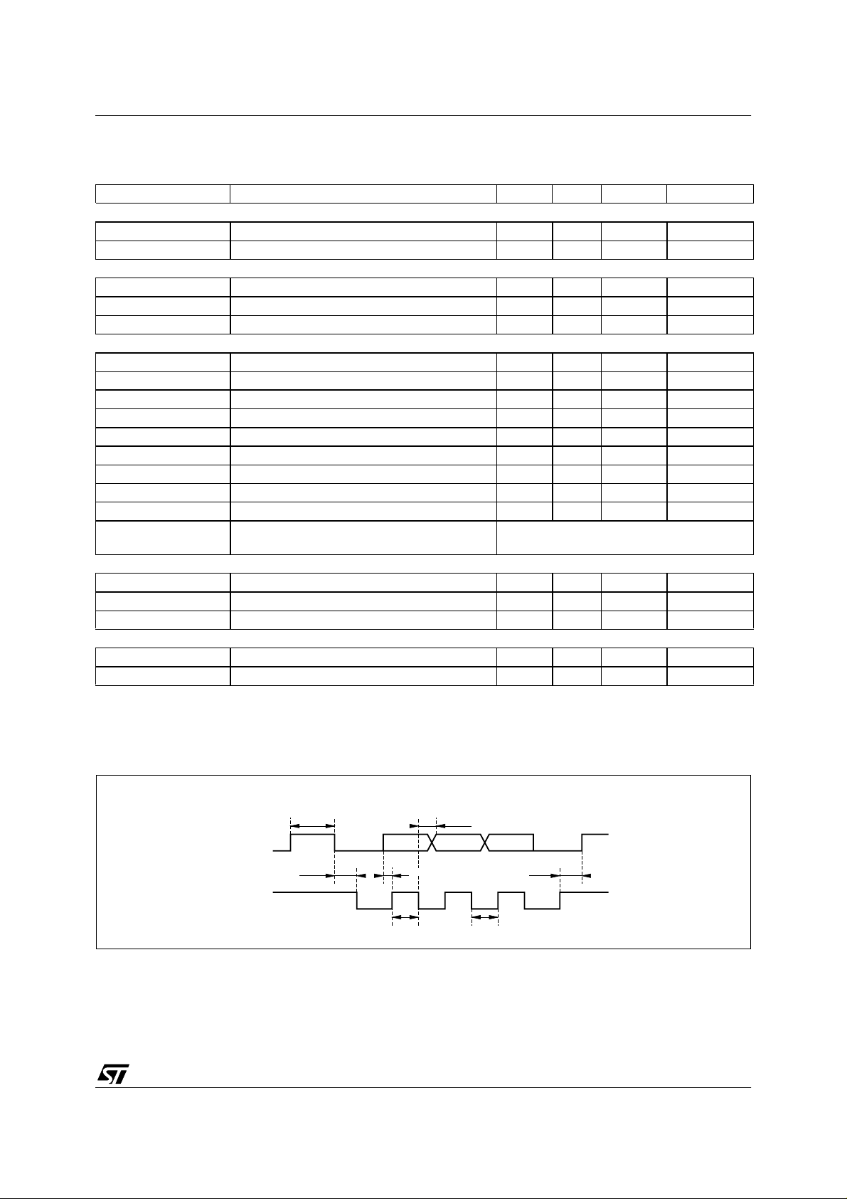
Figure 1.
STOP START DATA
t
BUF
SDA
t
HDS
SCL
t
HIGH
t
SUDAT
t
HDAT
t
LOW
t
SUP
STOP
5/24
2
Page 6
STV9432TA
6 - SERIAL INTERFACE
The 2-wires serial interface is an I2C interface. To be
connected to the I
address; the slave address of the STV9432TA is BA
(in hexadecimal).
A6 A5 A4 A3 A2 A1 A0 RW
1011101
2
C bus, a devic e mu st o wn its slave
- The two bytes of the internal address where the
MCU wants to write data(s),
- The successive bytes of data(s).
All bytes are sent MSB bit first and the write data
transfer is ended with a stop.
6.2 - DATA TRANSFER IN READ MODE
6.1 - DATA TRANSFER IN WRITE MODE
The host MCU can write data into the STV9432TA
registers or RAM.
To write data into the STVA9432TA after a start, the
MCU must send (Figure 2):
- First, the I
2
C address slave byte with a l ow le vel for
the R/W bit,
Figure 2. I2C Write Operation
SCL
SDA
SCL
D7 D6 D5 D4 D3 D2 D1 D0 D7 D6 D5 D4 D3 D2 D1 D0 D7 D6 D5 D4 D3 D2 D1 D0
SDA
Figure 3. I
SCL
SDA
Start
I2C Slave Address
2
C Read Operation
I2C Slave Address
R/W
A7 A6 A5 A4 A3 A2 A1 A0 - - A13 A12 A11 A10 A9 A8
ACK LSB Address ACK MSB Address ACKStart
ACK ACKData Byte 1 Data Byte 2 ACK Data Byte n Stop
R/W
A7 A6 A5 A4 A3 A2 A1
ACK
The host MCU can read data from the STV9432TA
registers, RAM or ROM.
To read data from the STV9432TA (Figure 3), the
MCU must send 2 different I
one includes the I
2
C slave address byte with R/W bit
2
C sequences. The first
at low level and the 2 internal address bytes.
The second one includes the I
2
C slave address byte
with R/W bit at high level and all the successive data
bytes read at successive addresses starting from the
initial address given by the first sequence.
A0
--
A13 A12
A10
A10A9A8
LSB Address ACK
MSB Address
ACK
Stop
6/24
2
SCL
SDA
Start
I2C Slave Address
D7 D6 D5 D4 D3 D2 D1 D0
R/W
*
ACK
Data Byte 1
D7 D6 D5 D4 D3 D2 D1 D0
ACK
Data Byte n
ACK
Stop
Page 7
6.3 - ADDRESSING SPACE
6.3.1 - General Mapping
STV9432TA registers, RAM and ROM are mapped in a 32K address space.
The mapping is:
STV9432TA
0000
03FF
0400
07FF
0800
3FFF
4000
403F
4040
7FFF
Important Notice:
1024 bytes RAM Descriptors and character codes
Empty Space
Character Generator ROM
Internal Registers
Empty Space
All 16 bits datas are mapped LSB byte at lower address and MSB byte at higher ad-
dress.
– Example: H1 12 bits register: @4000: 8 LSB bits - @4001: 4 MSB bits.
– Descriptors must also be written to RAM LSB byte first.
6.3.2 - I
2
C Registers Mapping
4000 H1 LSB 4022 Color 2
4001 H1 MSB 4023 Color 3
4002 H2 LSB 4024 Color 4
4003 H2 MSB 4025 Color 5
4004 H3 LSB 4026 Color 6
4005 H3 MSB 4027 Color 7
4006 H4 LSB 4028 Color 8
4007 H4 MSB 4029 Color 9
4008 H5 LSB 402A Color 10
4009 H5 MSB 402B Color 11
400A H6 LSB 402C Color 12
400B H6 MSB 402D Color 13
400C V1 LSB 402E Color 14
400D V1 MSB 402F Color 15
400E V2 LSB 4030 Line Duration
400F V2 MSB 4031 Top Margin
4010 V3 LSB 4032 Horizontal Delay
4011 V3 MSB 4033 Character Height
4012 RCI 4034 Display Control
4013 GCI 4035 Locking Time Constant
4014 BCI 4036 Capture Time Constant
4015 SBN 4037 Initial Pixel Period
4016 TIMG 4038-403E Reserved
4017-401F Reserved 403F RST
4020 Color 0 4040-7FFF Reser ved
4021 Color 1
7/24
Page 8
STV9432TA
7 - TIMING ANALYZER
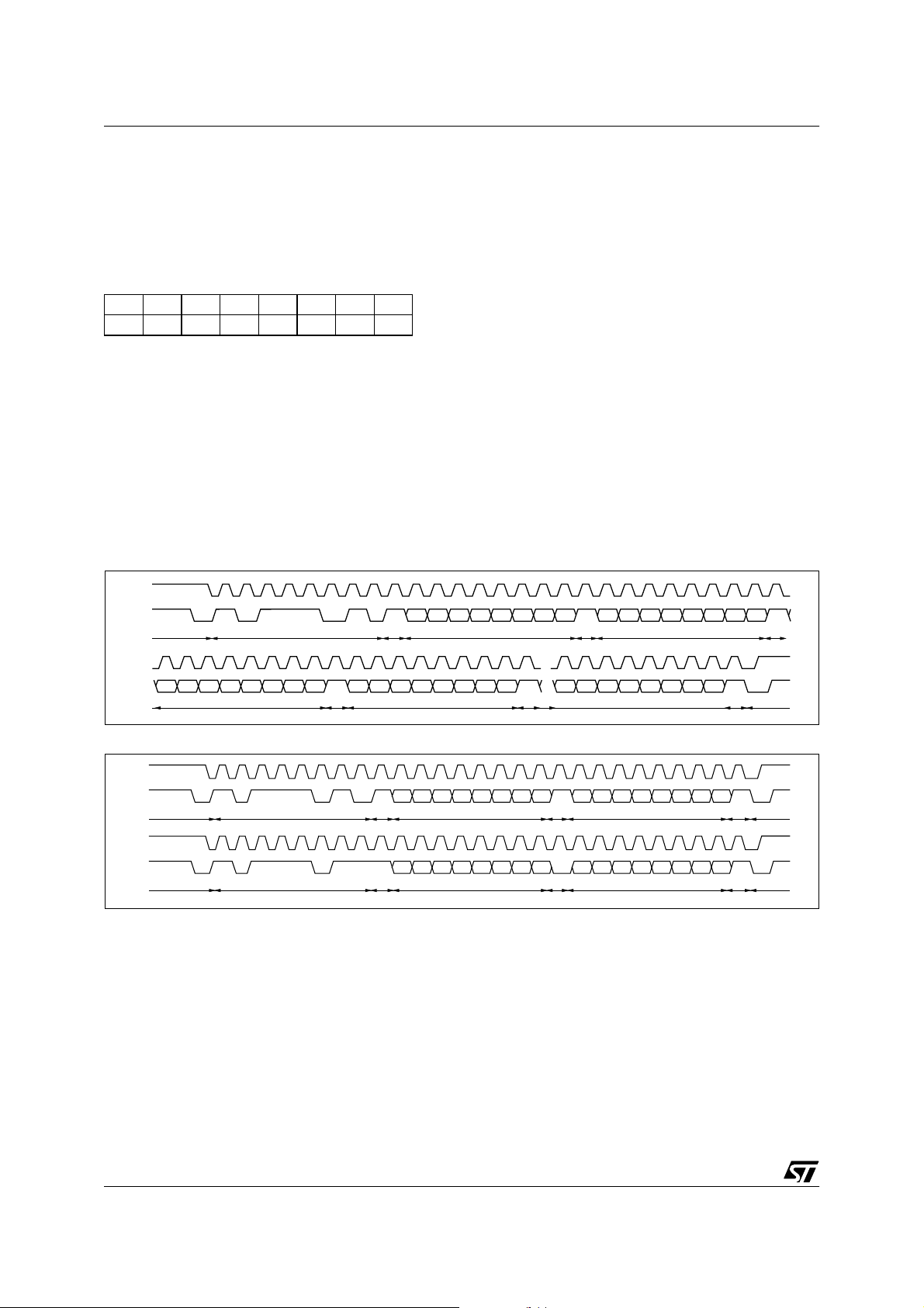
7.1 - Video Hori z ontal Timings
All horizontal timing measurements use a 106.7MHz clock. This clock is made from the internal oscillator:
f
= 40f
HTIM
They hold the value of the last measurement that was initiated by I2C command (see TIMG Register).
Figure 4.
: 3. These twelve bits read-only registers read time measurements, given in t
OSC
HTIM
units.
AV
HS
EE’
HFLY
AA’
L
F
B
K’K
L’
F’
H1 Register: H sync to Active video, min of C to A
4000 H1.7 H1.6 H1.5 H1.4 H1.3 H1.2 H1.1 H1.0
4001 - - - - H1.11 H1.10 H1.9 H1.8
H2 Register: Active video to H sync, min of B to C’
4002 H2.7 H2.6 H2.5 H2.4 H2.3 H2.2 H2.1 H2.0
4003 - - - - H2.11 H2.10 H2.9 H2.8
H3 Register: Line period, C to C’
4004 H3.7 H3.6 H3.5 H3.4 H3.3 H3.2 H3.1 H3.0
4005 - - - - H3.11 H3.10 H3.9 H3.8
H4 Register: H Fly to H sync, E to C
4006 H4.7 H4.6 H4.5 H4.4 H4.3 H4.2 H4.1 H4.0
4007 - - - - H4.11 H4.10 H4.9 H4.8
H5 Register: H sync to H Fly, C to E’
4008 H5.7 H5.6 H5.5 H5.4 H5.3 H5.2 H5.1 H5.0
4009 - - - - H5.11 H5.10 H5.9 H5.8
H6 Register: H fly pulse, E to F
400A H6.7 H6.6 H6.5 H6.4 H6.3 H6.2 H6.1 H6.0
400B - - - - H6.11 H6.10 H6.9 H6.8
7.2 - Video Ver t ical Ti m in gs
These twelve bits read-only registers read time measurements, given in number of scan lines. They hold the
value of the last measurement that was initiated by I
2
C command (see TIMG Register).
Figure 5.
8/24
AV
VS
AA’
B
K’K
L’L
3
Page 9

STV9432TA
V1 Register: V sync to Active video, min. of K to A
400C V1.7 V1.6 V1.5 V1.4 V1.3 V1.2 V1.1 V1.0
400D - - - - V1.11 V1.10 V1.9 V1.8
V2 Register: Active video to V sync, min. of B to K’
400E V2.7 V2.6 V2.5 V2.4 V2.3 V2.2 V2.1 V2.0
400F - - - - V2.11 V2.10 V2.9 V2.8
V3 Register: Number of lines per frame, K to K’7
4010 V3.7 V3.6 V3.5 V3.4 V3.3 V3.2 V3.1 V3.0
4011 - - - - V3.11 V3.10 V3.9 V3.8
7.3 - Timing Analysis Trigger
The Timing Analysis is performed according to the setting of SBN and TIMG registers :
7.3.1 - SBN Register
This 8 bits register holds the "sampling bloc" number.
The samp lin g bl oc is a se t of 4 consecuti ve sc an l ines , th e fir st of which is us ed fo r sam pl ing the v id eo timings or
Beam currents.
The reset value of this register is zero, must be programmed at a minimum value of 1 for correct operation.
4015 SBN7 SBN6 SBN5 SBN4 SBN3 SBN2 SBN1 SBN0
7.3.2 - TIMG Register
4016 STM NFR1 NFR0 ADCDLY3 ADCDLY2 ADCDLY1 0 SELECT
This 8 bits register holds the following parameters:
STM : Start Measurement Bit. This bit has to be forced to 1 by I2C to start the measurement
sequence, depending on the measurement selection bit. When measurement is com-
pleted the IC will reset this bit to 0.
NFR [1:0] : NFR number of measurement frames, 1 to 4 frames
ADCDLY[3:1] : Cut-off Beam current ADC sampling delay time: 0 to 15 x t
OSC
, by t
OSC
steps
SELECT : Selection of Beam current measurement (0) or Timing measurement (1)
To initiate a Timing Analysis cycle:
- program the Sampling Bloc Number in the SBN Register,
- program the TIMG Register, with: "SELECT" bit =1, "NFR" bits specify the number of measurement frames
(H1, H2, V1, V2), "STM" bit = 1 (Start Measurement).
As soon as the measurement cycle is finished, the "STM" bit is automatically reset by the device.
After a Timing Analysis cycle, reading a zero in STM bit of TIMG register means that the measurement is com-
pleted and the MCU may read the results in Hi and Vi registers. The reset value of this register is 0.
9/24
3
Page 10

STV9432TA
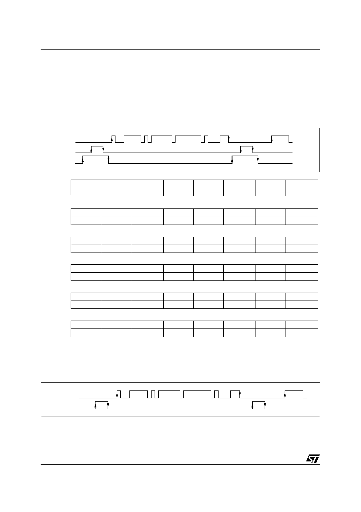
Figure 6. Video Timing Measurement seq uence - “Sele ct bit = 1” (TIMG register, bit 0)
I2C SET STM BIT (TIMG register)
WAIT FOR ACKNOWLEDGE BIT
WAIT FOR RISING EDGE OF VS
MEASURES H1 AT EVERY LINE
DURING NFR+1 FRAMES.
AFTER NFR+1 FRAMES,
H1 HOLDS THE MIN.VALUE
MEASURES H2 AT EVERY LINE
DURING NFR+1 FRAMES.
AFTER NFR+1 FRAMES,
H2 HOLDS THE MIN.VALUE
AFTER NFR+1 FRAMES, RESET STM BIT
MEASURES V3
MEASURES V1 DURING NFR+1
AND KEEPS THE MIN. VALUE
MEASURES V2 DURING NFR+1
AND KEEPS THE MIN. VALUE
WAIT FOR 4*SBN RISING ED G ES OF HS
AC QUISITION OF H3, H4, H5, H 6
10/24
3
Page 11

8 - BEAM CURRENTS MEA S UREMENT
8.1 - BEAM CURRENT MEASUREMENT REGISTERS
STV9432TA
The Beam Current Measurement circuitry uses three A to D converters, sampled at f
These three 8 bits registers read the values of t he l ast Beam currents measurement, initiated by I
frequency.
OSC
2
C com-
mand (see TIMG register).
RCI Register: Red Beam Current Input
4012 RCI7 RCI6 RCI5 RCI4 RCI3 RCI2 RCI1 RCI0
GCI Register: Green Beam Current Input
4013 GCI7 GCI6 GCI5 GCI4 GCI3 GCI2 GCI1 GCI0
BCI Register: Blue Beam Current Input
4014 BCI7 BCI6 BCI5 BCI4 BCI3 BCI2 BCI1 BCI0
8.2 - BEAM CURRENT MEASUREMENT TRIGGER
The Beam Currents Measurement is performed according to the setting of SBN and TIMG registers :
8.2.1 - SBN Register
This 8 bits register holds the "sampling bloc" number.
The sampling b loc is a set of 4 consecutive scan lines, the first of w hich is used f or sampl ing the video
timings or Beam currents. The reset value of this register is 0.
4015 SBN7 SBN6 SBN5 SBN4 SBN3 SBN2 SBN1 SBN0
8.2.2 - TIMG Register
4016 STM NFR1 NFR0 ADCDLY3 ADCDLY2 ADCDLY1 0 SELECT
This 8 bits register holds the foll owing parameters: To initiate a Beam Currents Measurement cycle:
STM : Start Measurement Bit. This bit
has to be forced to 1 by I
2
C to
start the measurement
sequence, depending on the
measurement selection bit.
When measurement is completed the IC will reset this bit to
0.
NFR [1:0] : NFR number of measurement
frames, 1 to 4 frames
ADCDLY
[3:1]
: Cut-off Beam current ADC sam-
pling delay time: 0 t o 14 x t
by t
OSC
steps
OSC
- program the Sampling Bloc Number in the SBN
Register,
- program the TIMG Register, with:
"SELECT" bit = 0, "ADCDLY" bits specify the
sampling time during HFly, "STM" bit = 1 (Start
Measurement).
As soon as the measurement cycle is finished, the
"STM" bit is automatica lly reset by the device. After a Beam Currents Meas urement cycle, read ing
a zero in STM bit of TIMG register mea ns that the
measurement is completed and the MCU may
read the results in RCI, GCI, and BCI registers.
The reset value of this register is 0.
,
SELECT : Selection of Be am current mea-
surement (0) or Timing measuremen t ( 1)
11/24
4
Page 12

STV9432TA
Figure 7. Beam Currents Measurement Sequenc e - “Select bit = 0” (TIMG register, bit 0)
I2C SET STM BIT (TIMG register)
WAIT FOR ACKNOWLEDGE BIT
WAIT FOR RISING EDGE OF VS
WAIT FOR 4*SBN RISING EDGES OF HS
WAIT FOR RISING EDGE OF HFLY
WAIT FOR ADC DLY
ACQUISITION OF RBC, GBC, BBC
RESET STM BIT
12/24
4
Page 13

STV9432TA
9 - SOFTWARE RESET REG IS TER
403F - - - - - - - RST
To perform a software I2C reset of the device, set the RST bit to ONE.
This bit will be au t omatically rese t by t he dev ic e .
Software Reset will put all Write registers at their default power-on value, and reset all internal logic
blocks except the I
2
C bus interface itself. It will not change the RAM contents.
SELXTAL This bit must b e set to ONE in order to operate the oscillator in the external crystal
mode.
In its ZERO default state, this bit enables the internal RC mode oscillator.
10 - ON-SCREEN DISPLAY
The STV9432TA on-screen display is able to display any line of characters (character strip) anywhere in the screen.
Character strings are programm ed by the MCU i n
RAM via I
2
C bus. Character shapes are coded in
the internal ROM font. Character strips may be
adjacent or separated by vertical spaces (Spacing
strips).
Consequently, one display page is made of a list
of Character strips and Spacing strips.
A Top Margin and a Left Margin are programmable
in dedicated registers.
Each Strip is associated with a 2 bytes Strip
Descriptor.
There are two Strip Descriptors:
- The Character Strip Descriptors containing the
Text string Ram address of the Character Strip,
- The Spacing Strip Descriptors which specify the
vertical space height.
In the example show n in Figure 8 on page 13, the
OSD screen, is made of 9 strips.
In RAM, there is:
- one list of 9 Strip descriptors
(size = 9 x 2 bytes = 18 bytes),
- 6 Text strings, each of them made of the character
10.1 - RAM PROGRAMMING
10.1.1 - Two kinds of Data:
Strip Descriptors and Character Codes
An OSD screen is made of a number of Character
and Spacing strips.
Two groups of Data make one OSD screen:
- a Strip Desc ript o rs li st ,
- Text strings - one per Character strip.
codes from the line of text.
Text strings can be programmed anywhere in
RAM. The Descriptor list can be located at 16 different addresses in RAM. The address is defined
in the Display Control Register. It is consequently
possible to store up to 16 different pages in RAM.
The current Displayed page is specified in the Display Control Register. It refers to a given Page
Descriptor list.
Figure 8. Display Page: List of Character and Spacing strips
TOP MARGIN
Text line number one
Text line number two
Text line number three
Text line number four
LEFT MARGIN
Text line number five
Text line number six
Strip 1 : Character Strip
Strip 2 : Character Strip
Strip 3 : Spacing Strip
Strip 4 : Character Strip
Strip 5 : Spacing Strip
Strip 6 : Character Strip
Strip 7 : Character Strip
Strip 8 : Character Strip
Strip 9 : Spacing Strip (Bottom Margin)
13/24
5
Page 14

STV9432TA
10.1.2 - Descriptors
Spacing
MSB 0
LSB SL7 SL6 SL5 SL4 SL3 SL2 SL1 SL0
L/ : LINE or CHARACTER spacing:
C
C
L/
= 0, spacing descriptor defined as character height (SL[7:0] = 1 to 255 character).
= 1, spacing descriptor defined as scan line height (SL[7:0] = 1 to 255 scan lines).
------
SL[7:0] : Number of selected height (character or scan lines according L/ ).
C
Character
MSB 1 DE CLU3 CLU2 CLU1 CLU0 C9 C8
LSB C7 C6 C5 C4 C3 C2 C1 C0
DE : Display enable:
= 0, R = G = B = 0 and FBLK = FBK bit of display control register on the whole strip,
= 1, display of the characters.
CLU[3:0] : Active color selection at the begining of the strip.
C[9:1] : Address of the first character code of the strip.
C0 : Address 0 must be 0.
10.1.3 - Code Format
There are basically 3 kinds of code:
- the control codes from 0 to 15 (00H to 0FH),
- the ROM monochrome character codes from 16 to 255 (10H to FFH),
- the two bytes multicolor character codes from 08F0 to 08FF (Hex).
For code definitions see Table 1.
Table 1 Character and Command Codes
0 123456789ABCDEF
0 col 0
1 col 1
2 col 2
3 col 3
4 col 4
5 col 5
6 col 6
7 col 7
8 multicol
9nop
A vflip
B hflip
C dflip
D call
E rtn
F eof
Single byte codes 00 to 0f are command codes. Single byte codes 10 to ff are monochrome character codes.
Double byte codes 08F0 to 08FF are multicolor character codes.
240 Monochrome Characters
14/24
5
Page 15

Figure 9. Character Font of the STV9432TA
STV9432TA
15/24
5
Page 16

STV9432TA
Control Codes
Control codes must be followed by a displayable
code, except for RTN & EOL. They must not be
used twice consecutively without a displayable
code between them.
The control code CALL is preceded by an address
byte. The control codes are not displayed except if
mentioned.
Codes 0 to 7 (0h to 7h):
COL0 to COL7 codes select 1 byte among 8
within the CLUT in RAM. The block selection is
fi xe d by CLU 3 b i t of t he a ct i v e c h ar ac t er d es cr i p to r
(see Table 1 and Table 2).
Code 8 (08h):
Multicolor character precode, must be followed by
a multicolor character number from F0h to FFh.
Code 9 (09h):
NOP: no operation is performed, can be used to
spare a location in RAM for an active control code.
Codes 10 to 12 (0Ah to 0Ch):
FLIPS:
HFLIP(0Bh)
Horizontal Flip code flips horizontaly
the following displayable code.
VFLIP(0Ah)
Vertical Flip code flips verticaly the
following displayable code.
DFLIP(0Ch)
Horizontal & Vertical Flip code flips
horizontaly and verticaly the following displayabl e
code.
Code 13 (0Dh):
CALL, this control code switches the display of t he
next character to the code address given by the
next byte as follows:
CALL CODE
@) MSB
(odd
ADDRESS BYTE
(even
@) LSB
00001101
A8 A7 A6 A5 A4 A3 A2 A1
A[9:1] : Address of the next code to
be used (A0 = 0 only even
addresses), in low h alf part of
RAM.
Notes:
CALL and RTN code must be used simultaneously.
CALL and RTN codes are displayed as a SPACE
character.
CALL and RTN codes must be placed at odd addresses. They may be preceded by a NOP to place
them at the right position.
Code 14 (0Eh):
RTN: return to the CALL + 1 code l ocation (see
Note).
Code 15 (0Fh):
EOL, end of line terminates the display of the cur-
rent row.
ROM Character Codes
Codes 16 to 255 (10h to FFh):
ROM monochrome character codes. The c haracter shapes are 12x18 pixel matrix described in Fig -
ure 9 .
Codes 256 to 272 (F0h to FFh):
ROM multicolor character codes. They must be
preceded by the multicolor pre-code 08h. The
character shapes are 12x18 pixel matrix
described in F igure 9.
10.2 - OSD LOOK-UP TABLE
Color look-up table [CLUT] is read/write RAM
table. Mapping address is described in Chapter
6.3.2 -
I2C Registers Mapping
on page 7.
The CLUT is splitted into 2 blocks of 8 byt es. Each
byte contains foreground and background informations as described below:
TRA BR BG BB FL FR FG FB
TRA
FL
BR, BG, BB
FR, FG, FB
:
Transparent background
:
Flashing foreground
:
Background color
:
Foreground color
Each block may store a different set of colors. One
block of colors may be used f or the normal items
of the menu while the second block, with brighter
colors, may be used for selected items of the
menu.
The block selection is done by programming bit
CLU3 of CLU[3:0] of the character descriptor (see
Table 2). It remains selected for the whole row.
Bit CLU2, CLU1 and CLU0 of CLU[3:0] of the
character descriptor select the active color at the
beginning of the row.
The active color can be modified along the row,
using 8 control codes COL0 to COL7.
Each control code (COL0 to COL7) activates a
dedicated color byte in the CLUT as described in
Table 2.
16/24
5
Page 17

Table 2 CLUT Block Selection
CLU3 CLU[2:0] Code Name Command
0 Col 0 00 @4020 07
1 Col 1 01 @4021 16
0 2 Col 2 02 @4022 25
3 Col 3 03 @4023 34
4 Col 4 04 @4024 43
5 Col 5 05 @4025 52
6 Col 6 06 @4026 61
7 Col 7 07 @4027 70
0 Col 0 00 @4028 70
1 Col 1 01 @4029 61
2 Col 2 02 @402A 52
1 3 Col 3 03 @402B 43
4 Col 4 04 @402C 34
5 Col 5 05 @402D 25
6 Col 6 06 @402E 16
7 Col 7 07 @402F 07
10.3 - OSD CONTROL REGISTERS
Code (hex)
STV9432TA
Ram @(hex) Reset Value
(hex)
Line Duration (reset value: 20H)
4030 VSP HSP LD6 LD5 LD4 LD3 LD2 LD1
VSP : V-SYNC active edge selection
= 0, falling egde,
= 1, rising edge.
HSP : HFLY active edge selection
= 0, rising egde,
= 1, falling edge.
LD[6:1] : LINE DURATION
LD0 = 0
LD1 = 2 periods of character
One character period is 12 pixels long.
Top Margin (reset value: 30H)
4031 M9 M8 M7 M6 M5 M4 M3 M2
M[9:2] : TOP MARGIN height from the VSYNC reference edge.
M0 = 0, M1 = 0
M2 = 4 scan lines
Note : The top margin is displayed before the first strip of descriptor list. It can be black if FBK of DISPLAY
CONTROL register is set or transparent if FBK is clear.
17/24
5
Page 18

STV9432TA
Horizontal Delay (reset value: 20H)
4032 DD7 DD6 DD5 DD4 DD3 DD2 DD1 DD0
DD[7:0] :
HORIZONTAL DISPLAY DELAY from the HSYNC reference edge to the 1
ter strips.
Unit = 6 pixel periods. Minimum value is 08H. First pixel position = [DD[7:0] - 6] x 6 + 54 with
DD[7:0] = 0,2,4,6 delay is 54 pixel and with DD[7:0] = 1,3,5 delay is 60 pixel
st
pixel position of the charac-
Characters Height (reset value: 24H)
4033 - - CH5 CH4 CH3 CH2 CH1 CH0
CH[5:0] : HEIGHT of the character strips in scan lines. For each scan line, the number of the slice which is dis-
played is given by:
SLICE-NUMBER =
(
round
SCAN-LINE-NUMBER = Number of the current scan line of the strip.
SCAN-LINE-NUMBER x 18
CH[5:0]
)
Display Control (reset Value: 00H)
4034 OSD FBK FL1 FL0 P9 P8 P7 P6
OSD : ON/OFF (if 0, R, G, B and FBLK outputs are 0).
FBK : Fast blanking control:
= 1, forces FBLK pin at "1" outside and inside the OSD area.
This leads to blank video RGB and to only display OSD RGB.
= 0, FBLK pin is driven according character code for normal display of OSD data.
FL[1:0] : Flashing mode :
- 00: No flashing. The character attribute is ignored,
(50% duty cycle),
F
F
F
st
descriptor of the current displayed pages.
P[9:6] :
- 01: Flashing at f
- 10: Flashing at 2 f
- 11: Flashing at 4 f
Note: fF is 128 time vertical frequency.
Address of the 1
P[13:10] and P[5:0] = 0; up to 16 different pages can be stored in the RAM.
Locking Condition Time Constant (reset value : 01H)
4035 FR AS2 AS1 AS0 LUK BS2 BS1 BS0
FR : Free Running; if = 1 PLL is disabled and the pixel frequency keeps its last value.
AS[2:0] : Phase constant during locking conditions.
BS[2:0] : Frequency constant during locking conditions.
LUK : Lock unlock status bit
0 = unlocked PLL
1 = Locked PLL
18/24
5
Page 19

STV9432TA
C
C
Capture Process Time Constant (reset value: 24H)
4036 LEN AF2 AF1 AF0 - BF2 BF1 BF0
LEN : Lock enable
0 = R,G,B, FBLK are always enabled,
1 = R,G,B,, FBLK are enabled only when PLL is locked.
AF[2:0] : Phase constant during the capture process.
BF[2:0] : Frequency constant during the capture process.
Initial Pixel Period (reset value: 06H)
4037 PP7 PP6 PP5 PP4 PP3 PP2 PP1 PP0
PP[7:0] : Value to initialize the pixel period of the PLL.
10.4 - OSD TIMINGS
The number of pixel periods is given by the LINE
DURATION register and is equal to:
[LD[6:1] x 2 + 1 ] x 12.
(LD[6:1]: value of the LINE DURATION register).
This value is used to define the horizontal size of
the characters.
The horizontal left margin is given by the HORIZONTAL DELAY register and is equal to:
(DD[7:0] -6) x 6 + 54
(DD[7:0]: value of the DISPLAY DELAY register).
This value is used to define the horizontal position
of the characters on the screen. Due to internal
logic, minimum horizontal delay is fixed at 4.5
characters (54 pixel) when DD is even and inferior
or equal to 6, and it is f ixed at 5 characters (60
pixel) when DD is odd and inferior or equal to 7.
10.5 - PLL
The PLL function of the STV9432TA provides the
internal pixel clock locked on the horizontal synchro signal and used by the d isplay processor to
generate the R, G, B and fast blanking signals. It
is made of 2 PLLs. The first PLL which is analog
(see Figure 10) provides a high frequency that is
40 times the internal oscillator frequency, or
320MHz. This high frequency clock is used by th e
Display controller.
The 320MHz frequency is then divided by three.
The resulting 106.7MHz clock is used by the
Video timings analysis block.
The second PLL, fully digital (see Figure 11), provides a pixel frequency locked on the horizontal
synchro signal. The ratio between the frequencies
of these 2 signals is:
M = 12 x (LD[6:1] x 2 + 1) where LD[ 6:1] is the
value of the LINE DURATION register.
Figure 10. An al og P LL
N • f
OS
VCO 40
FILTER
f
OSC
Figure 11. Digi t al PLL
M • f
H-SYNC
40 • f
OSC
%D %M
ALGO
f
H-SYN
err(n)D(n)
10.5.1 - Programming of the PLL Registers
Initial Pixe l Pe riod (@4037)
This register allows to increase the speed of the
PLL convergence when the horizontal frequency
changes (new graphic standard).
The relationship between PP[7:0], LD[6:1], f
and f
PP[7:] = round
OSC
is:
(
40 . f
OSC
6. (2 . LD + 1) . f
HSYNC
HSYNC
)
19/24
5
Page 20

STV9432TA
f
f
t
f
f
t
f
f
f
f
Locking Condition Time Constant
(@ 4035)
This register provides the AS[2:0] and BS[2:0]
constants used by the algo part of the PLL (see
Figure 10). These two constants as well as the
phase error (err(n)) give the new value (Dn) of the
high frequency signal division. Consequently,
AS[2:0] and BS[2:0] fix the pixel cloc k frequency.
These two constants are used only in locking condition, if the phase error is inferior to a fixed value
during at least 4 scan lines. If the phase error
becomes superior to the fixed value, the PLL is
not in locking condition but in capture process. In
this case, the algo part of the PLL uses the other
constants AF[2:0] and BF[2:0] from the next register.
Capture Process Time Constant
(@ 4036)
The choice between these two time constants
(locking condition or capture process) allows to
decrease the capture process time by changing
the time response of the PLL.
10.5.2 - How to choose the time constant value
The time response of the PLL i s given by its characteristic equation which is:
2
(x - 1)
+ ( ) . (x - 1) + = 0
αβ+ β
Where:
. 2A -11
α 3LD⋅= β
[6:1]
and = 3 . LD[6:1] . 2
B - 19
(LD[6:1] = value of the LINE DURATION register,
A = value of the 1st time constant, AF or AS and
B = value of the 2
d
time constant, BF or BS).
As can be seen, the solution depends only on the
LINE DURATION and the TIME CONSTANTS
given by the I
2
C registers.
If ( )
ble and its response is as shown in Figure 15.
If ( )
shown in Figure 13. In this case the PLL is stable
τ
if > 0.7 damping coefficient.
Table 3 gives some g ood values f or A and B con-
stants for different values of the LINE DURATION.
Figure 12. Time Response of the PLL/
Characteristic equation solutions (with real
solutions)
Figure 13. Time Response of the PLL/
Characteristic equation solutions (with
complex solutions)
2
αβ+ β0≥αβ
αβ+ β0≤
- 4 and 2 < 4, the PLL is sta-
2
- 4 , the response of the PLL is as
PLL Frequency
1
0
Input Frequency
1
0
PLL Frequency
1
0
Input Frequency
1
0
–
Table 3 Valid Time Constants Examples
B \ A 0 1 2 3 4 5 6
0 YYYY YYYY YYYY YYYN YNNN NNNN NNNN
1 YYYY YYYY YYYY YYYN YNNN NNNN NNNN
2 NYYY YYYY YYYY YYYN YNNN NNNN NNNN
3 NNNY YYYY YYYY YYYN YNNN NNNN NNNN
4 NNNN NYYY
5 NNNN NNNY YYYY YYYN YNNN NNNN NNNN
6 NNNN NNNN NYYY YYYN YNNN NNNN NNNN
7 NNNN NNNN NNNY YYYN YNNN NNNN NNNN
(1)
YYYY YYYN YNNN NNNN NNNN
t
t
Case of A[2:0] = 1 (001) and B[2:0] = 4 (100)
:Table meaning: N = No possible capture - No stability, Y = PLL can lock.
LD[6:1] 8 16 24 32
Valid Time Constants NYYY
20/24
5
Page 21

11 - APPLICA T IO N DIAGRAM
Figure 14.
I2C bu s
Horizontal syn c
Vertival sync
Fly back pulse
Active video
C1
100pF
100pFC2100pFC3100pF
Beam cu rrent inputs
Separate path for digitlal GN D
1kΩ
R2
R3 R4
1kΩ
100pF
2.2kΩ
R1
1nF
TEST 24
ADCREF 23
RCI 22
GCI 21
BCI 20
AVdd 19
OVdd 18
FBLK 17
BOUT 16
GOUT 15
ROUT 14
OVss 13
100nF
22pF
1 FILTER
2 AGND
3 SDA
4 SCL
5 HS
6 VS
7 HFLY
8 AV
9 DVdd
10 DVss
11 XTi
12 XTO
C8
L1
100
C7
m
H
Xtal
C4
8 Mhz
22pF
C5 C6
22µF
C11
100nF
C10
100nF
C9
C12
100
L2
m
H
C14 C14
100pF
VDD +5VGND
1kΩ
47µF
C16
100pF
100nF
C15
L3
100mH
RGB outputs
Fast blanking ouput
STV9432TA
21/24
5
Page 22

STV9432TA
22/24
Page 23

12 - PACKAGE MECHANICAL DATA
24 PINS - PLASTIC DIP (SHRINK)
B eB1
D
A1
Stand-off
A2
STV9432TA
E
E1
LA
e1
e2
c
E
24
1
13
F
12
SDIP24
.015
0,38
Gage Plane
e3
e2
Dimensions Millimeters Inches
Min. Typ. Max. Min. Typ. Max.
A 5.08 0.20
A1 0.51 0.020
A2 3.05 3.30 4.57 0.120 0.130 0.180
B 0.36 0.46 0.56 0.0142 0.0181 0.0220
B1 0.76 1.02 1.14 0.030 0.040 0.045
C 0.23 0.25 0.38 0.0090 0.0098 0.0150
D 22.61 22.86 23.11 0.890 0.90 0.910
E 7.62 8.64 0.30 0.340
E1 6.10 6.40 6.86 0.240 0.252 0270
e 1.778 0.070
e1 7.62 0.30
e2 10.92 0.430
e3 1.52 0.060
L 2.54 3.30 3.81 0.10 0.130 0.150
23/24
6
Page 24

Information furnished is believed to be accurate and reliable. However, STMicroelectronics assumes no
responsibility for the consequenc es of use of such information nor f or any infringemen t of patents or oth er
rights of third parties which may result from its use. No license is granted by implication or otherwise under any
patent or patent rights of STMicroelectronics. Specifications mentioned in this publication are subject to change
without notice. This publication supersedes and replaces all information previously supplied.
STMicroelectronics products are not authorized for use as critical components in life support devices or
systems without express written approval of STMicroelectronics.
The ST logo is a trademark of STMicroelectronics.
© 2000 STMicroelectronics - All Rights Reserved
2
Purchase of I
Rights to use these components in a I
C Components of STMicroelectronics, conveys a license under the Philips I2C Patent.
2
C system, is granted provided that the system conforms to the I2C
Standard Specifications as defined by Philips.
STMicroelectronics GROUP OF COMPANIES
Australia - Brazil - China - Finland - France - Germany - Italy - Japan - Korea - Malaysia - Malta - Mexico - Morocco - The
Netherlands - Singapore - Spain - Sweden - Switzerland - Taiwan - Thailand - United Kingdom - U.S.A.
http://www.st.com
24/24
7
 Loading...