

Page 1
MULTISYNCH ON-SCREEN DISPLAY FOR MONITOR
.
CMOS SINGLE CHIP OSD FOR MONIT OR
.
BUILT IN 1 KBYTE RAM HOLDING :
- CHARACTER CODES
- USER DEFINABLE CHARACTERS
.
207 ALPHANUMERIC CHARACTERS OR
GRAPHIC SYMBOLS IN INTERNAL ROM
.
12 x 18 CHARACTER DOT MATRIX
.
PROGRAMMABLE ACCENTUA TED CHARACTER SET
.
CHARACTER BLINKING
.
RAM DEFINABLE COLOR LOOK UP TABLE
.
UP TO 16 USER DEFINABLE CHA RACTE RS
.
UP TO 80MHz PIXEL CLOCK
.
INTERNAL HORIZONTAL PLL (15 TO 120kHz )
.
PROGRAMMABLE VERTICAL HEIGHT OF
CHARACTER WITH A SLICE INTERPOLATOR
TO MEET MULTI-SYNCH REQUIREMENTS
.
PROGRAMMABLE VERTICAL AND HORIZONTAL POSITIONING
.
FLEXIBLE SCREEN DESCRI PT ION
.
22 CONTROL CODES FOR POWERFULL
SERIAL ATTRIBUTES
.
2-WIRES ASYNCHRONOUS SERIAL MCU
INTERFACE (I
.
8 x 8 BITS PWM DAC OUTPUTS
.
SINGL E PO SITIVE 5V SUPPLY
2
C PROTOCOL)
STV9427
STV9428-STV9429
HIGH SPEED
8 x 8 bits PWM DAC are available to provide DC
voltage control to other peripherals.
The STV9427/28/29 provides the user an easy to
use and cost effective solution to display alphanumeric or graphic information on monitor screen.
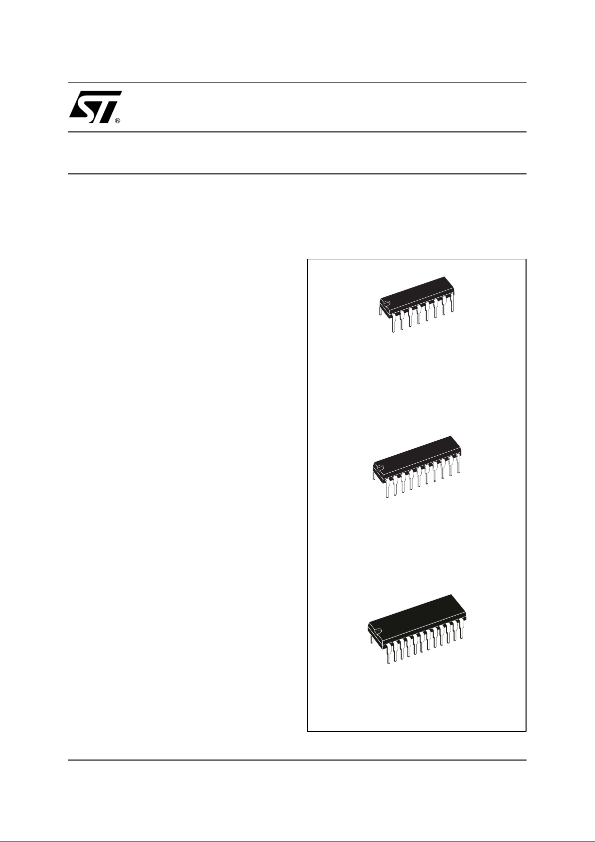
DIP16
(Plastic Package)
ORDER CODE :
(Plastic Package)
STV9427
DIP20
DESCRIPTION
The STV9427/28/29 is an ON SCREEN DISPLAY
for monitor. It is built as a slave peripheral connected to a host MCU via a serial I
includes a display memory, controls all the display
attributes and generates pixels from the data read
in its on chip memory. The line PLL and a special
slice interpolator allow to have a display aspect
which does not depend on the line and frame
frequencies. I
transparent internal access to prepare the next
pages during the display of the current page. Toggle from one page to another by programming only
one register.
June 1998
2
C interface allows MCU to make
2
C bus. It
ORDER CODE : STV9428
DIP24
(Plastic Package)
ORDER CODE :
STV9429
1/20
Page 2
STV9427 - STV9428 - STV9429
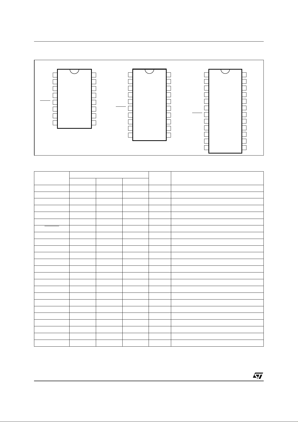
PIN CONNECTIONS
V
DD1
TST
XTO
XTI
RESET
VSYNC
HSYNC
GND
DIP16 (STV9427)
1
2
3
4
5
6
7
8
16
15
14
13
12
11
10
V
DD2
B
G
R
FBLK
GND
SDA
SCL
9
PWM1
RESET
VSYNC
HSYNC
PWM2
DIP20 (STV9428)
1
2
V
DD1
3
TST
XTI
4
5
6
7
8
9
10
XTO
GND
20
PWM0
19
V
DD2
18
B
17
G
16
R
15
FBLK
14
GND
13
SDA
12
SCL
11
PWM3
PWM6
PWM1
V
DD1
TST
XTO
XTI
RESET
VSYNC
HSYNC
GND
PWM2
PIN DESCRIPTION
Symbol
DIP24 DIP20 DIP16
PWM6 1 - - O DAC0 Output
PWM1 2 1 - O DAC1 Output
V
DD1
3 2 1 S +5V Logic Supply
TST 4 3 2 I Reserved (not to be connected)
XTO 5 4 3 O Crystal Output
XTI 6 5 4 I Crystal or Clock Input
RESET 7 6 5 I Reset Input (Active Low)
VSYNC 8 7 6 I Vertical Sync Input
HSYNC 9 8 7 I Horizontal Sync Input
GND 10 9 8 S Logic Ground
PWM2 11 10 - O DAC2 Output
PWM5 12 - - O DAC3 Output
PWM4 13 - - O DAC4 Output
PWM3 14 11 - O DAC5 Output
SCL 15 12 9 I Serial Clock
SDA 16 13 10 I/O Serial Input/output Data
GND 17 14 11 S Ground
FBLK 18 15 12 O Fast Blanking Output
R 19 16 13 O Red Output
G 20 17 14 O Green Output
B 21 18 15 O Blue Output
V
DD2
22 19 16 S +5V Outputs Supply
PWM0 23 20 - O DAC6 Output
PWM7 24 - - O DAC7 Output
Pin Number
I/O Description
DIP24 (STV9429)
1
2
3
4
5
6
7
8
9
10
11
12
24
23
22
21
20
19
18
17
16
15
14
13
PWM7
PWM0
V
DD2
B
G
R
FBLK
GND
SDA
SCL
PWM3
PWM4PWM5
9427-01.TBL 9427-01.EPS / 9428-01.EPS / 9 429-01.EPS
2/20
Page 3
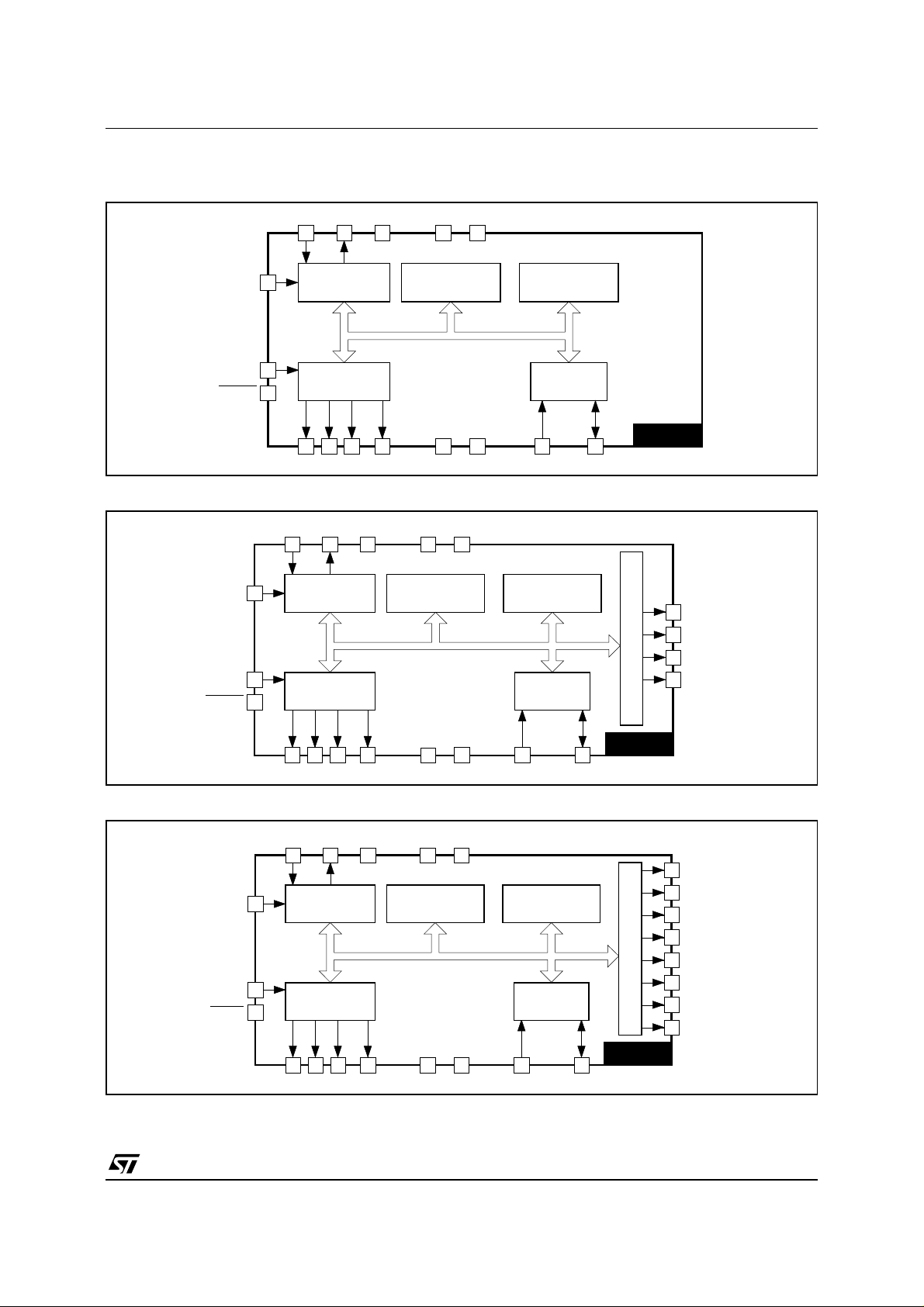
BLOCK DIAGRAMS
STV9427
XTI XTO
TST V
234
V
DD1
1
STV9427 - STV9428 - STV9429
DD2
16
STV9428
HSYNC
VSYNC
RESET
HSYNC
VSYNC
RESET
7
6
5
XTI XTO TST
5 4 3
HORIZONTAL
8
DIGITAL PLL
7
CONTROLLER
6
HORIZONTAL
DIGITAL PLL
4K ROM
1K RAM
Address/Data
DISPLAY
CONTROLLER
12
RGBFBLK GND SCL
V
2
4K ROM
Address/Data
DISPLAY
GND
DD1
1113 14 15
8
V
DD2
19
2
I C BUS
INTERFACE
9 10
1K RAM
I2C BUS
INTERFACE
SDA
STV9427
20
11
PWM
10
1
9427-02.EPS
PWM0
PWM3
PWM2
PWM1
STV9429
HSYNC
VSYNC
RESET
16 17 18 15 14 12 13
RGBFBLK GND SCL SDA
XTI XTO TST
6 5 4
HORIZONTAL
9
DIGITAL PLL
Address/Data
8
7
DISPLAY
CONTROLLER
19 20 21 18 17 15 16
RGBFBLK GND SCL SDA
9
GND
V
DD1
3
4K ROM
10
GND
V
DD2
22
INTERFACE
1K RAM
I2C BUS
STV9428
PWM
STV9429
24
23
14
13
12
11
2
1
9428-02.EPS
PWM7
PWM0
PWM3
PWM4
PWM5
PWM2
PWM1
PWM6
9429-02.EPS
3/20
Page 4
STV9427 - STV9428 - STV9429
ABSOLUTE MAXIMUM RATINGS
Symbol Parameter Value Unit
V
DD
V
IN
T
OPER
T
STG
ELECTRICAL CHARACTERI STICS
= V
(V
DD1
Symbol Parameter Min. Typ. Max. Unit
SUPPLY
V
DD
I
DD
INPUTS
SCL, SDA, RESET, VSYNC and HSYNC
V
IL
V
IH
I
IL
OUTPUTS
SDA open drain and PWMi (i = 0 to 7)
V
OL
V
OH
R, G, B, FBLK
V
OL
V
OH
Supply Voltage -0.3, +7.0 V
Input Voltage -0.3, +7.0 V
Operating Temperature 0, +70 °C
Storage Temperature -40, +125 °C
= 5V, VSS = 0V, TA = 0 to 70°C, f
DD2
= 8 to 15MHz, TEST = 0 V, unless otherwise s p ec ified)
XTAL
Supply Voltage 4.75 5 5.25 V
Supply Current - 65 90 mA
Input Low Voltage 0.8 V
Input High Voltage 2.4 V
Input Leakage Current -10 +10 µA
Output Low Voltage (IOL = 1.6mA) 0 0.4 V
Output High Voltage (IOH = -0.1mA) 0.9V
DD
V
DD
Output Low Voltage (IOL = 1.6mA) 0 0.4 V
Output High Voltage (IOH = -0.1mA) 0.9V
DD
V
DD
9427-02.TBL
V
V
9427-03.TBL
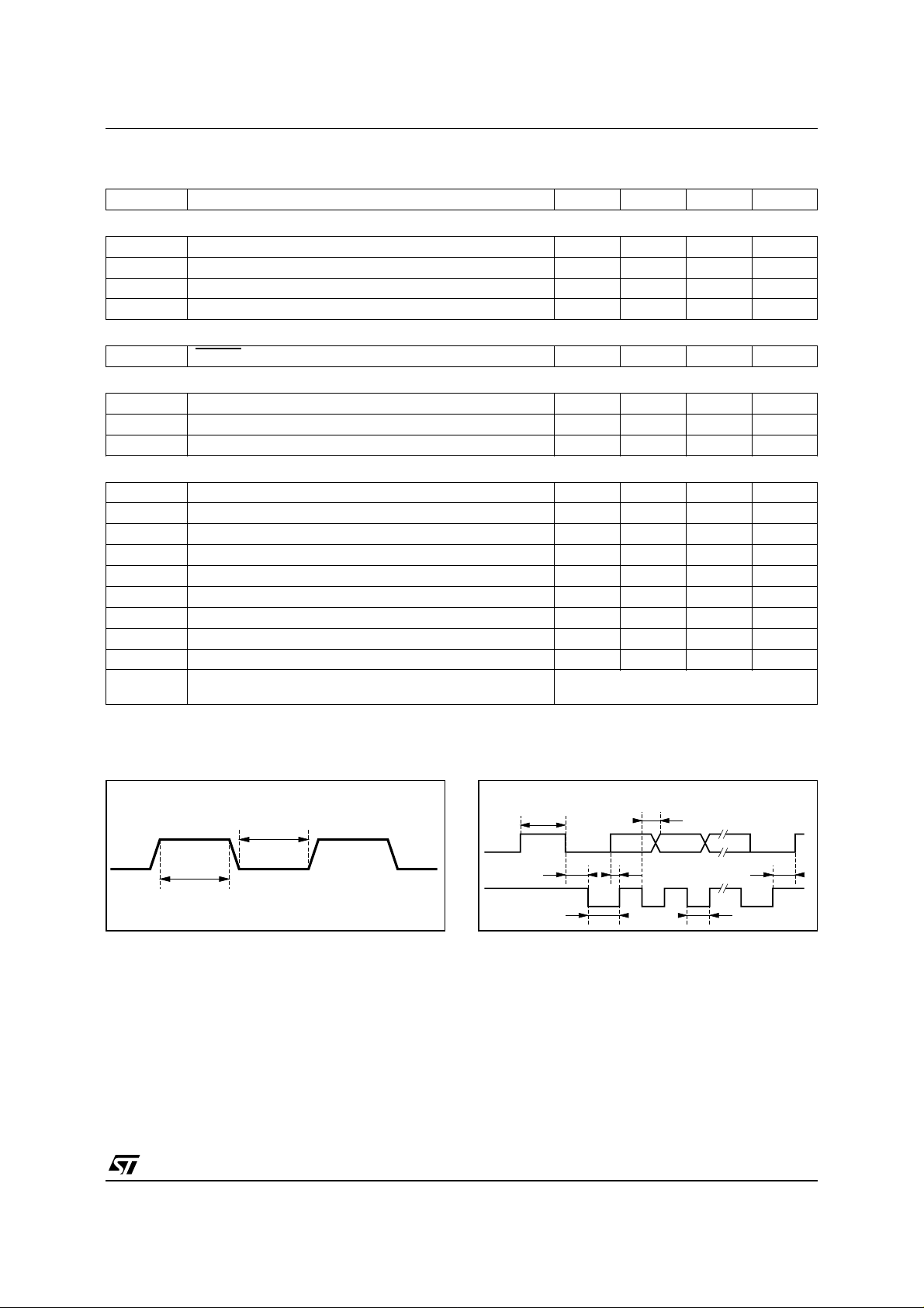
Figure 1 :
V
OL OH
5
2.5
0
-5
10
4/20
R, G, B, FBLK Typical Outputs Static
Characteristics
(V)
V
,
V
OH
V
OL
I (A)
10
-4
10
-3
10
-2
10
-1
9427-17.EPS
Page 5
STV9427 - STV9428 - STV9429
TIMINGS
Symbol Parameter Min. Typ. Max. Unit
OSCILATOR INPUT : XTI (see Figure 2)
t
WH
t
WL
f
XTAL
f
PXL
RESET
t
RES
R, G, B, FBLK (C
t
R
t
F
t
SKEW
2
C INTERFACE : SDA AND SCL (see Figure 3)
I
f
SCL
t
BUF
t
HDS
t
SUP
t
LOW
t
HIGH
t
HDAT
t
SUDAT
t
F
t
R
Note 1 :
Clock High Level 20 ns
Clock Low Level 20 ns
Clock Frequency 6 15 MHz
Pixel Frequency 30 80 MHz
RESET Low Level Pulse 4 µs
= 30pF)
LOAD
Rise Time (see Note 1) 5 ns
Fall Time (see Note 1) 5 ns
Skew between R, G, B, FBLK 5 ns
SCL Clock Frequency (Horizontal frequency = 32kHz) 288 kHz
Time the bus must be free between 2 access 500 ns
Hold Time for Start Condition 500 ns
Set up Time for Stop Condition 500 ns
Clock Low Level 400 ns
Clock High Level 400 ns
Hold Time Data 0 ns
Set up Time Data 500 ns
SDA Fall Time 20 ns
SCL and SDA Rise Time
These parameters are not tested on each unit. They are measured during our internal qualification procedure whic h i ncludes
characterization on batches comming from corners of our processes and also temperature characterization.
Depend on the pull-up resistor
and on the load capacitance
9427-04.TBL
Figure 2
XTI
Figure 3
Stop Start Data Stop
t
t
BUF
HDS
t
WL
t
WH
SDA
SCL
t
9427-03.EPS
HIGH
t
SUDAT
t
HDAT
t
SUP
t
LOW
9427-04.EPS
5/20
Page 6
STV9427 - STV9428 - STV9429
FUNCTIONAL DESCRIPTION
The STV9427/28/29 display processor operation is
controlled by a host MCU via the I
fully programmable through internal read/write registers and performs all the display functions by
generating pixels from data stored in its internal
memory. After the page downloading from the
MCU, the STV9427/28 /29 refreshes screen by
its built in p rocessor, without a ny MCU control
(access). In addition, the host MCU has a direct
access to the on c hip 1Kbytes RAM du ring the
display of the curr ent page to make any update
of its c ontents.
With the STV9427/28/29, a page displayed on the
screen is made of several strips which can be of 2
types : spacing or character and which are described by a table of descriptors and character
codes in RAM. Several pages can be downloaded
at the same time in the RAM and the choice of the
current display page is made by programming the
DISPLAY CONTROL register.
I - Serial Interface
The 2-wires serial interface is an I
be connected to the I
2
C bus, a device must own its
slave address ; the slave address of the
STV9427/28/29 is BA (in hexadecimal).
A6 A5 A4 A3 A2 A1 A0 R/W
1011101
2
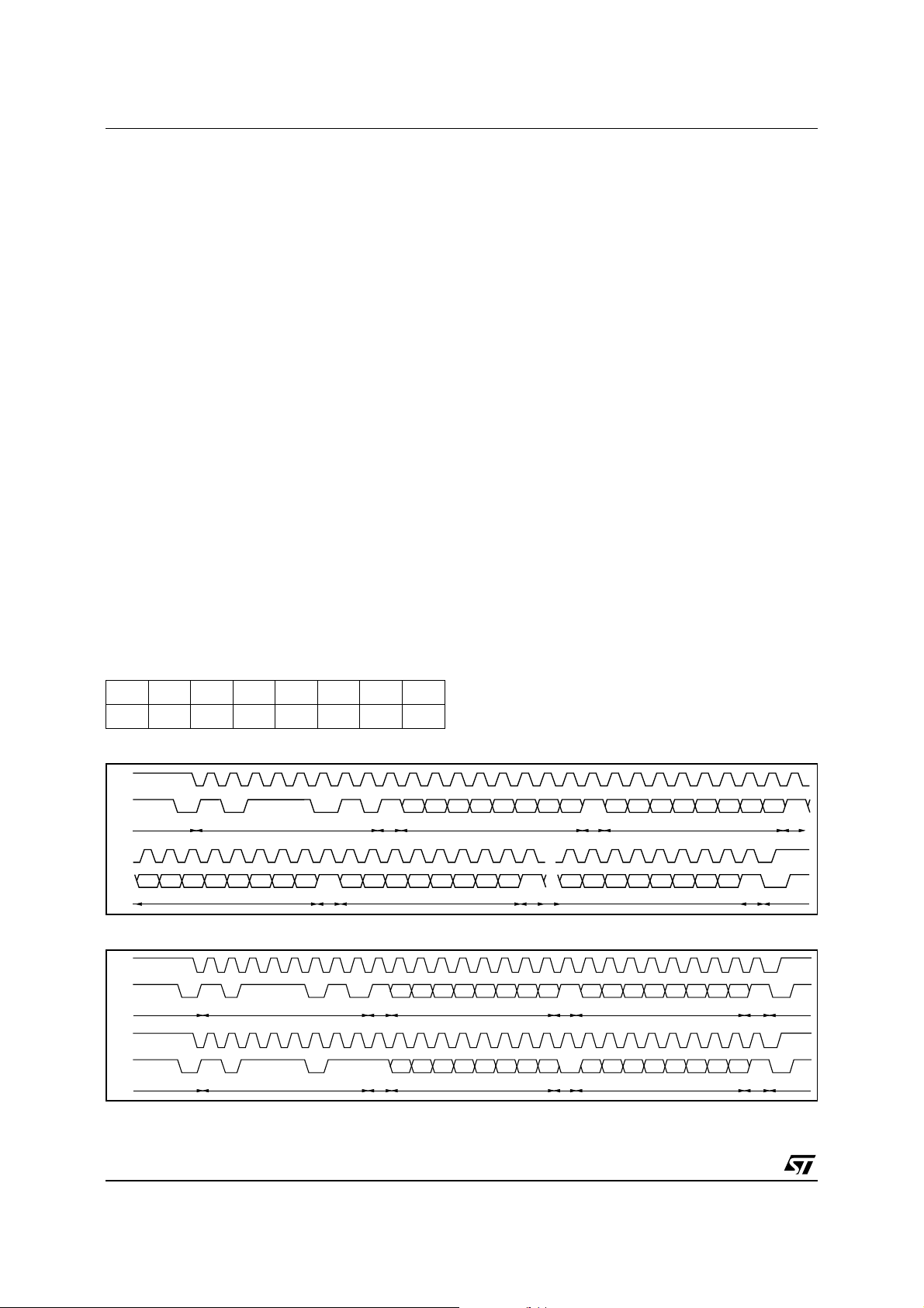
Figure 4 :
MCU I
C Write Operation
2
C interface. It is
2
C interface. To
I.1 - Data Transfer in Write Mode
The host MCU can write data into the
STV9427/28/29 registers or RAM.
T o write data into the STV9427/28/29, after a start,
the MCU must send (Figure 4) :
- First, the I
2
C address slave byte with a low level
for the R/W bit,
- The two bytes of the internal address where the
MCU wants to write data(s),
- The successive bytes of data(s).
All bytes are sent MSB bit first and the write data
transfer is closed by a stop.
Each byte is synchronously transfered at each
HSYNC period.
I.2 - Data Transfer in Read Mode
The host MCU can read data from the
STV9427/28/29 registers, RAM or ROM.
To read data fr om the STV9427/28/29 (Figure 5),
the MCU must send 2 different I
first one is made of I
2
C slave address byte with R/W
bit at low level and the 2 internal address bytes.
The second one is made of I
2
C sequences. The
2
C slave address byte
with R/W bit at high le vel and all the successive
data bytes read at successive addresses starting
from the initial address given by the first sequence.
Each byte is synchronously transfered at each
HSYNC period. The first data byte, in read mode,
is available one Hsync period after the acknowledge of the address byte.
SCL
R/W
SDA
I2C Slave Address
SCL
D7 D6 D5 D4 D3 D2 D1 D0 D7 D6 D5 D4 D3 D2 D1 D0 D7 D6 D5 D4 D3 D2 D1 D0
SDA
ACK ACKData Byte 1 Data Byte 2 ACK Data Byte n Stop
2
Figure 5 :
SCL
SDA
SCL
SDA
Note :
MCU I
Start
Start
The first data bit out (D7) is valid after one scanline period.
C Read Operation
R/W
I2C Slave Address
R/W
I2C Slave Address
A7 A6 A5 A4 A3 A2 A1 A0 - - A13 A12 A11 A10 A9 A8
ACK LSB Address ACK MSB Address ACKStart
A7 A6 A5 A4 A3 A2 A1
ACK
D7 D6 D5 D4 D3 D2 D1 D0
*
ACK
LSB Address ACK
Data Byte 1
A0
--
A13 A12
MSB Address
D7 D6 D5 D4 D3 D2 D1 D0
ACK
Data Byte n
6/20
A10
A10
9427-05.EPS
A9
A8
ACK
Stop
ACK
Stop
9427-06.EPS
Page 7

STV9427 - STV9428 - STV9429
FUNCTIONAL DESCRIPTION
(continued)
I.3 - Addressing Space
I.3.1 - General Mapping
STV9427/28/29 registers, RAM and ROM are
mapped in a 16Kbytes addressing space. The
mapping is the following :
0000
03FF
0400
07FF
0800
3FBF
3FC0
3FD0
3FCF
3FD0
1024 bytes RAM
Character Generator
Internal Registers
Empty Space
ROM
Empty Space
Descriptors character
codes and user
definable characters
I.3.2 - I2C Registers Mapping
3FCF
3FD0 PWM0
PWM1
PWM2
PWM3
PWM4
PWM5
PWM6
3FD7 PWM7
3FD8
Reserved
3FDF
3FE0 Color 0
Color 1
Color 2
Color 3
Color 4
Color 5
Color 6
3FE7 Color 7
3FE8 Color 8
Color 9
Color 10
Color 11
Color 12
Color 13
Color 14
3FEF Color 15
3FF0 Line Duration
Top Margin
Horizontal Delay
Character Height
Display Control Control registers
Locking Time Constant
Capture Time Constant
Initial Pixel period
3FF8 Frequency Multiplier
3FF9
Reserved
3FFF
PWM registers
Color look-up
table (CLUT)
I.4 - Register Set
I.4.1 - PWM Registers
The eight registers described below are only available with the STV9429 :
PULSE WIDTH MODULATOR 0 (STV9429)
3FD0 V07 V06 V05 V04 V03 V02 V01 V00
st
V0[7:0] : Digital value of the 1
PWM D to A converter.
PULSE WIDTH MODULATOR 1 (STV9429)
3FD1 V17 V16 V15 V14 V13 V12 V11 V10
nd
V1[7:0] : Digital value of the 2
PWM DAC.
PULSE WIDTH MODULATOR 2 (STV9429)
3FD2 V27 V26 V25 V24 V23 V22 V21 V20
rd
V2[7:0] : Digital value of the 3
PWM DAC.
PULSE WIDTH MODULATOR 3 (STV9429)
3FD3 V37 V36 V35 V34 V33 V32 V31 V30
th
V3[7:0] : Digital value of the 4
PWM DAC.
PULSE WIDTH MODULATOR 4 (STV9429)
3FD4 V47 V46 V45 V44 V43 V42 V41 V40
th
V4[7:0] : Digital value of the 5
PWM DAC.
PULSE WIDTH MODULATOR 5 (STV9429)
3FD5 V57 V56 V55 V54 V53 V52 V51 V50
th
V5[7:0] : Digital value of the 6
PWM DAC.
PULSE WIDTH MODULATOR 6 (STV9429)
3FD6 V67 V66 V65 V64 V63 V62 V61 V60
V6[7:0] : Digital value of the 7
th
PWM DAC.
PULSE WIDTH MODULATOR 7 (STV9429)
3FD7 V77 V76 V75 V74 V73 V72 V71 V70
th
V7[7:0] : Digital value of the 8
Note :
Power on reset default value of PMW register is 00H
PWM DAC.
7/20
Page 8

STV9427 - STV9428 - STV9429
FUNCTIONAL DESCRIPTION
(continued)
I.4.2 - Look-up Table Regist e r s
Color look-up table [CLUT] is read/write RAM table.
Mapping address is described in Chapter I.3.2.
The CLUT is splitted in 2 blocks of 8 bytes. Each
byte contains foreground and background informations as described below :
SHA BR BG BB FL FR FG FB
SHA : Shadowing
FL : Flashing foreground
BR, BG, BB : Background color
FR, FG, FB : Foreground color
If SHA = 1 and BR = BG = BB = 0, the background
of the character is transparent.
Each block may store a different set of colors. One
block of colors may be used for the normal items
of the menu while the second block, with brighter
colors, may be used for selected items of the menu.
The block selection is done by programming bit
CLU3 of CLU[3:0] of the character descriptor
(see Table 1). It remains selected all the row long.
Bit CLU2, CLU1 and CLU0 of CLU[3:0] of the
character descriptor select the active color at the
beginning of the row.
The active color can be changed along the row,
using 8 control codes COL0 to COL7.
Each c ontrol code (COL0 to COL 7) active a dedica ted
color byte in the CL UT as descri bed in Table 2.
T ab le 1 :
CLU3 CLU[2:0]
CLUT Block Selection
0 Col 0 @3FE0 07
1 Col 1 @3FE1 16
2 Col 2 @3FE2 25
0
1
3 Col 3 @3FE3 34
4 Col 4 @3FE4 43
5 Col 5 @3FE5 52
6 Col 6 @3FE6 61
7 Col 7 @3FE7 70
0 Col 0 @3FE8 70
1 Col 1 @3FE9 61
2 Col 2 @3FEA 52
3 Col 3 @3FEB 43
4 Col 4 @3FEC 34
5 Col 5 @3FED 25
6 Col 6 @3FEE 16
7 Col 7 @3FEF 07
Code
Name
Ram
@(hex)
Reset Value
(hex)
Table 2 :
CLUT Color Selection
Code
Name
COL1 10 @ 3FE0 : Color 0
COL2 11 @ 3FE1 : Color 1
COL6 16 @ 3FE6 : Color 6
COL7 17 @ 3FE7 : Color 7
COL0 10 @ 3FE8 : Color 8
COL1 11 @ 3FE9 : Color 9
COL6 16 @ 3FEE : Color 14
COL7 17 @ 3FEF : Color 15
Code Nbr
(h)
Color Look-up Table in
RAM
I.4.3 - Control Registers
LINE DURATION (Reset Value : 20h)
3FF0 VSP HSP LD6 LD5 LD4 LD3 LD2 LD1
VSP : V-SYNC active edge selection
= 0, falling egde,
= 1, rising edge.
HSP : H-SYNC active edge selection
LD[6:1] : LINE DURATION
= 0, falling egde,
= 1, rising edge.
LD0 = 0
LD1 = 2 periods of character
One character period is 12 pixels long.
TOP MARGIN (Reset Value : 60h)
3FF1 M8 M7 M6 M5 M4 M3 M2 M1
M[8:1] : T OP MARGIN height from the VSYNC reference
Note :
edge.
M0 = 0
M1 = 2 scan lines
The top margin is displayed before the first strip of descriptor
list. It can be black if FBK of DISPLAY CONTROL register is
set or transparent if FBK is clear.
HORIZONTAL DELAY (Reset Value : 20h)
3FF2 DD7 DD6 DD5 DD4 DD3 DD2 DD1 DD0
DD[7:0] : HORIZONTAL DISPLAY DELAY from the
HSYNC reference edge to the 1
of the character strips.
Unit = 6 pixel periods. Minimum value is 08h.
First pixel position = [DD[7:0] - 6] x 6 + 54.
with DD[7:0] = 1,3,5 then the delay is 60 pixel.
st
pixel position
8/20
Page 9

STV9427 - STV9428 - STV9429
FUNCTIONAL DESCRIPTION
(continued)
CHARACTERS HEIGHT (Reset Value : 24h)
3FF3 - - CH5 CH4 CH3 CH2 C H1 CH0
CH[5:0] : HEIGHT of the character strips in scan li nes. For
each scan line, the number of the slice which is
displayed is given by :
SLICE-NUMBER =
SCAN−LINE−NUMBER x 18
round
SCAN-LINE-NUMBER = Number of the current
scan line of the strip.
CH[5:0]
.
DISPLAY CONTROL (Reset Value : 00h)
3FF4 OSD FBK FL1 FL0 P9 P8 P7 P6
OSD : ON/OFF (if 0, R, G, B and FBLK outputs are 0).
FBK : Fast blanking control :
FL[1:0] : Flashing mode :
P[9:6] : Address of the 1
= 1, forces FBLK pin at "1" outside and inside the
OSD area. This leads to blank video RGB and
to only display OSD RGB.
= 0, FBLK pin is driven according character code
for normal display of OSD data.
00 : No flashing.
-
The character attribute is ignored,
01 : Flashing at fF (50% duty cycle),
-
10 : Flashing at 2 fF,
-
11 : Flashing at 4 fF.
-
Note : f
displayed pages.
P[13:10 ] an d P [5:0] = 0 ; up to 1 6 d if f ere nt pa ges
can be stored in the RAM.
is 128 time vertical frequency.
F
st
descriptor of the current
LEN : Lock enable
AF[2:0] : Phase constant during the capture process.
BF[2:0] : Frequency constant during the capture process.
0 = R,G,B, FBLK are always enabled,
1 = R,G,B, FBLK are enabled only when PLL is
locked.
INITIAL PIXEL PERI OD (Reset Value : 28h)
3FF7 PP7 PP6 PP5 PP4 PP3 PP2 PP1 PP0
PP[7:0] : Value to initialize the pixel period of the PLL.
FREQUENCY MULTIPLIER (Reset Value : 0Ah)
3FF8----FM3FM2FM1FM0
FM[3:0] : Frequency multiplier of the crystal frequency to
Note : For high pixel frequency (over 70MHz), write at address 3FFF,
Data F0h.
reach the high frequency used by the PLL to
derive the pixel frequency.
II - Descriptors
SPACING
MSB 0 L/C-----LSB SL7 SL6 SL5 SL4 SL3 SL2 SL1 SL0
C : LINE or CHARACTER spacing :
L/
SL[7:0] : Number of selected height (character or scan
= 0, spacing descriptor defined as character
height (SL[7:0] = 1 to 255 character).
= 1, spacing descriptor defined as scan line
height (SL[7:0] = 1 to 255 scan lines).
lines according L/
C).
LOCKING CONDITION TIME CONSTANT
(Reset Value : 01h)
3FF5 FR AS2 AS1 AS0 LUK BS2 BS1 BS0
FR : Free Running ; if = 1 PLL is disabled and the pixe l
frequency keeps its last value.
AS[2:0] : Phase constant during locking conditions.
BS[2:0] : Frequency constant during locking conditions.
LUK : Lock unlock status bit
0 = unlocked PLL
1 = Locked PLL
CAPTURE PROCE SS TIME CO NS TANT
(Reset Value : 24h)
3FF6 LEN AF2 AF1 AF0 - BF2 BF1 BF0
CHARACTER
MSB 1 DE CLU3 CLU2 CLU1 CLU0 C9 C8
LSBC7C6C5C4C3C2C1UEN
DE : Display enable :
= 0, R = G = B = 0 and FBLK = FBK bit of display
control register on the whole strip,
= 1, display of the characters.
CLU[3:0] : Active color selection at the begining of the
strip.
C[9:1] : Address of the first character code of the strip.
UEN : UDC enable
0 : codes 240 to 254 (FOh to FEh) are read in
ROM,
1 : codes 240 to 255 (FOh to FFh) are read in
RAM (UDC).
9/20
Page 10

STV9427 - STV9428 - STV9429
FUNCTIONAL DESCRIPTION
(continued)
III - Code Format
The codes of STV9427/28/29 are all single byte
codes. There are basically 3 kinds of code :
- The control codes from 0 to 27 (00h to 1Bh) and
from 224 to 239 (E0h to EFh).
- The ROM character codes from 32 to 223 (20h to
DFh) and from 240 to 255 (F0h to FFh).
- The user definables characters codes f rom 240
to 254 (F0h to FFh).
Each row must begin with a displayable character
code followed by a NOP or any control code.
For code definition see Table 4.
III.1 - Control Codes
Control codes must be followed by a displayable
code (from 32 to 223), except for RTN & EOL. They
must not be used twice consecutively without a
displayable code between them.
The control code CALL is preceded by an address
byte.
The control codes are not displayed except if mentioned.
Code 0 (00h) :
Codes 1 to 7
(01h to 07h)
NOP : no operation and no display is
performed, can be used to spare a
location in RAM for an active control
code.
SYMETRIES :
:
TSHS(01)
Symetry code displays the top half
side of the following displayable code
symetricaly to the bottom side.
BSHS(02)
Symetry code displ ays the bottom hal f
side of the following displayable code
symetricaly to the top side.
HFLIP(03)
horizontaly the following displayable
code.
LSVS(04)
code displays the left half side of the
following displayable code
symetricaly to the right side.
RSVS(05)
code displays the ri ght h alf si de o f the
following displayable code
symetricaly to the left side.
VFLIP(06)
verticaly the following displayable
code.
HVFLIP(07)
code fl i ps h oriz ont al y a nd ver ti cal y the
following displayable code.
Top Side Horizontal
Bottom Side Horizontal
Horizontal Flip code flips
Left Side Vertical Symetry
Right Side V ertical symetry
Vertical Flip code flips
Horizontal & Vertical Flip
Codes 8 (08h)
(at odd @)
Code 09 to 14
RTN : return to the CALL + 1 code
:
location (see Note).
Reserved
:
(09h to 0Eh)
Code 15 (0Fh) :
Codes 16 to 23
(10h to 17h)
Codes 24 to 27
(18h to 19h)
CALL CODE
(odd @) MSB
ADDR ESS BYTE
(even @) LSB
A[9:1] : Address of the next code to be used ( A0 = 0 o nl y even
Notes :
CALL and RTN code must be used twin. They cannot be nested.
CALL and RTN codes are displaye d as a SPACE charact er.
CALL and RTN codes must be placed at odd addresses. They may
be preceed by a NOP in order to place them at the right position.
addresses).
Codes 28 to 31
EOL, end of line terminates the
display of the current row.
COL0 to COL7 codes select 1 byte
:
among 8 within the CLUT in RAM. The
block selection is fixed by CLU3 bit of
the active character descriptor (see
Table 1 and Table 2).
CALL, these control codes switch the
:
display of the next character to the
code address given by the next byte
as following :
0001100A9
A8 A7 A6 A5 A4 A3 A2 A1
Reserved
:
(1Ch to 1Fh)
Code 224 to 239
(E0h to EFh)
Accent shapes from 224 to 239 (E0h
:
to EFh) are used combined with all
other character codes 32 to 223 (10h
to DFh) and placed before the target
character.
The first set of accents, 224 to 231 (E0h
to E7h) m ust b e us ed w ith low er cas e
letters. The 5 upper slices of the target
charact er are replaced by th e accent
shape.
The secon d set o f acc ent s, 23 2 t o 23 9
(E8h to EFh) must be used with the
upper ca se let ters (capi tal lette rs). The
3 upper slices of the target character
are replaced by the accent shape.
Accent code must always be followed
by a displ aya bl e ch aract er or a sp ace .
III.2 - ROM Character Codes
Codes 32 to 223
(20h to DFh) and
Codes 240 to 254
(F0h to FEh)
: ROM character shapes are
described as 12x18 pixel matrix as
shown in Table 5.
It comprises 60 logos dedicated for
monitor application (Horizontal
position, keystone, ...), 25 cha racters
for horizontal bar-graph and
additional shapes.
10/20
Page 11

STV9427 - STV9428 - STV9429
FUNCTIONAL DESCRIPTION
(continued)
Table 4
Code N° MSB 0 1 2 3 4 5 6 7 8 9 10 11 12 13 14 15
LSB HEX 0 1 2 3456 7 8 9 A B C D E F
0 0 NOP COL0 Space 0 @ P ¢ p Ç Cont1 Hlin1 Box0 Bar5 Bar21 ’ dn R
1 1 TSHS COL1 ! 1 A Q a q ç Cont2 Hlin2 Box1 Bar6 Bar22 ’ up G
2 2 BSHS COL2 " 2 B R b r Æ Bright Kystn Box2 Bar7 10o ^ dn B
3 3 HFLIP COL3 # 3 C S c s æ Color Kybal1 Box3 Bar8 1o0 x dn 1
4 4 LSVS COL4 $ 4 D T d t Ø Spkr Kybal2 Box4 Bar9 Indxrgt∼ dn 2
5 5 RSVS COL5 % 5 E U e u ø Mute Pincus Box5 Bar10 Indxup ° up clock0
6 6 VFLIP COL6 & 6 F V f v ß Dgaus Pinbal Box6 Bar11 rtn dot dn clock1
7 7 HVFLIP COL7 ’ 7 G W g w « Balance Tilt1 Box7 Bar12 hbar0
8 8 RTN CALL ( 8 H X h x 1/2 Vfcus Tilt2 Box8 Bar13 hbar1 ’ up A
99-CALL
10 A - - * : J Z j z 3/4 Vsz Cornr1 Box10 Bar15 vbar1 ^ up T
11 B - - + ; K [ k {
12 C - - , < L ® l |
13 D - - - = M © m << fh Hsz Cornr4 Bar2 Bar18 mic ° up L
14 E - - .
15 F EOL - / ? O _ o Arr up hz Hpos2 hz Bar4 Bar20 upidx1
±
9 I Y i y 1/4 Hfcus Cornr0 Box9 Bar14 vbar0 ‘ up E
≈
Vpos Cornr2 Bar0 Bar16 treble x up S
≡
Vlin Cornr3 Bar1 Bar17 bass∼ up Z
÷
N ¥ n Arr If fv Hpos1 kh Bar3 Bar19 upidx0 dot up D
..
dn clock2
..
up
9427-09.TBL
11/20
Page 12

STV9427 - STV9428 - STV9429
FUNCTIONAL DESCRIPTION
III.3 - User Definable Character Codes
(continued)
(UDC)
Codes 240 to 254 (F0h to FEh) refer to character shape loaded in RAM.
The STV9427/28/29 allows the user to dynamically define c haracter(s) for his own needs (for a special
LOGO for example). Like the ROM characters, a UDC is made of a 12 pixels x 18 slices dot matrix.
In a UDC, each pixel is defined with a bit, 1 refers to foreground, and 0 to background color. Each slice of
a UDC uses 2 bytes :
add + 1 - - - - PX11 PX10 PX9 PX8
add (even) PX7 PX6 PX5 PX4 PX3 PX2 PX1 PX0
PX1 1 is t he l eft m ost pixe l. Cha rac ter s lice addr ess : SLICE ADDRE SS = 64 (CHARACTER NUMBE R - 240)
+ (SLICE NUMBER + 7) x 2.
Where :
- CHARACTER NUMBER is the number given by the character code.
- SLICE NUMBER is the number given by t he slice interpolator (n° of the current slice of the strip : 1 <<18).
Figure 6 :
Code Number Ram Location
Code 240/F0h
Code 241/F1h
Code 242/F2h
Code 243/F3h
Code 244/F4h
Code 245/F5h
Code 246/F6h
Code 247/F7h
Code 248/F8h
Code 249/F9h
Code 250/FAh
Code 251/FBh
Code 252/FCh
Code 253/FDh
Code 254/FEh
Code 255/FFh
User Definable Character Codes
hex dec
00 00
3F
63
40
64
7F
127
80
128
BF
191
C0
192
FF
255
100
256
319
140
320
383
180
384
447
1C0
448
511
200
512
575
240
576
639
280
640
703
2C0
704
767
300
768
831
340
832
895
380
896
959
3C0
960
1023
UDC LOCATION CHARACTER ORGANIZATION
Slice Offset
hex dec hex dec
01 00
03 02
05 04
07 06
09 08
0B 11 0A 10
0D 13 0C 12
0F 15 0E 14
11 17 10 16
19 18
21 20
23 22
25 24
27 26
29 28
31 30
21 33 20 32
35 34
37 36
39 38
41 40
43 42
45 44
47 46
31 49 30 48
51 50
53 52
55 54
57 56
59 58
61 60
3F 63 3E 62
Unused
Unused
Unused
Unused
Unused
Unused
Unused
Slice 0
Slice 1
Slice 2
Slice 3
Slice 4
Slice 5
Slice 6
Slice 7
Slice 8
Slice 9
Slice 10
Slice 11
Slice 12
Slice 13
Slice 14
Slice 15
Slice 16
Slice 17
Unused
Unused
Unused
Unused
Unused
Unused
Unused
SLICER ORGANIZATION
xxxx111098765432 01
MSB LSB
9427-18.EPS
12/20
Page 13

STV9427 - STV9428 - STV9429
FUNCTIONAL DESCRIPTION
Figure 7 :
Hozizontal Timing
(continued)
HSYNC
R, G, B
1678081
LD[6:1] = 40
DD[7:0] = 10
6.5
Nber of characters
of the row
IV - Clock and Timing
The whole timing is derived from the XTI a nd the
horizontal SYNCHRO input frequencies. The XTI
input frequency can be an external clock, crystal
or a ceramic re sonator signal th anks to XTI/XTO
pins. The value of this frequen cy can be chosen
between 6 and 15MHz is used by the PLL to
generate a pixel clock locked on the horizontal
synchro input s ignal.
IV.1 - Horizontal Timing
(see Figure 7)
The number of pixel periods is given by the LINE
DURATION register and is equal to :
[LD[6:1] x 2 + 1 ] x 12.
(LD[6:1] : value of the LINE DURA TI ON register).
This value allows to define the horizontal size of the
characters.
The horizontal left margin is given by the HORIZONTAL DELAY register and is equal to :
(DD[7:0] -6 ) x 6 + 54
(DD[7:0] : value of the DISPLAY DELAY register).
This value allows to define the hor izontal position
of the characters on the screen. Due to internal
logic, minimum horizontal delay is fixed at 4.5
characters (54 pixel) when DD is even and lower
or equal to 6, and it is fixed at 5 characters (60 pixel)
when DD is odd and lower or equal to 7.
IV .2 - D to A Timing
(STV9427)
The D/A converters of the STV9427 are pulse width
modulator converter.
f
The frequency of the output signal is :
Vi[7:0]
the duty cycle is :
256 x 6
per cent.
XTAL
256 x
and
6
After a low pass filter, the average value of the
Vi [7:0]
output is :
256 x 6
⋅ V
DD
V - Display Control
A screen is composed of successive scanlines gath-
Active OSD Video
ered in several strips. Each strip is defined by a
descriptor stored in memory. A table of descriptors
allows screen composition and different tables can
be stored in memory at the page addresses
(16 possible ≠ addresses). Two types of strips are
available :
- Spacing strip : its descriptor (see II) gives the
number of black (FBK = 1 in DISPLAY CONTROL
register) or transparent (FBK = 0) lines.
- Character strip : its descriptor gives the memory
address of the character codes corresponding to
st
the 1
displayed character. The characters and
attributes (see code format III) are de fined by a
succession of codes stored in the RAM at addresses starting from the 1
st
one given by the
descriptor. A character st rip can be displayed or
not by using the DE bit of its descriptor.
After the VSYNC edge, the first strip descriptor is
read at the top of the current table of descriptors at
the address given by P[9:0] (see DISPLAY CONTROL register) ; if it is a spacing strip, SL[7:0] black
or transparent scan lines are displayed ; if it is a
character strip, during CH[5:0] scan lines (CH[5:0]
given by the CHARACTER HEIGHT register), the
character codes are read at the addresses starting
from the 1
st
one given by the descriptor until a end
of line character or the end of the scan line ; the
next descriptor is then read and the same process
is repeated until the next edge of VS YNC.
0
1
PWM Timing
PWM1 Signal
T
XTAL
256 . T
XTAL
Figure 8 :
V1[7:0]
128
255
9427-07.EPS
9427-08.EPS
13/20
Page 14

STV9427 - STV9428 - STV9429
FUNCTIONAL DESCRIPTION
Figure 9 :
Figure 10 :
Relation between Screen/Address Page/Character Code in RAM
DISPLAY CONTROL Register
FL1 P8 P7 P6P9
OSD FBK
2nd CHARACTER
STRIP CODES
FL0
OTHER
TABLE OF
DESCRIPTORS
OTHER
(UDC for example)
1st CHARACTER
STRIP CODES
rd
CHARACTER
3
SRTIP CODES
OTHER
(CODES OR
DESCRIPTORS)
RAM CODE
AND DESCRIPTORS
User Definable Character
ON THE SCREEN
36 Pixels (= 3 Characters)
123
36 Slices (= 2 Characters)
456
(continued)
V-SYNC
SPACING
ROW1
ROW2
SPACING
ROW3
SPACING
TABLE OF THE
DESCRIPTORS
Height of Top Margin is given by TOP MARGIN Register
Note :
TOP MARGIN (see note)
TOP SPACING STRIP
st
1
CHARACTER STRIP
nd
2
CHARACTER STRIP
SPACING STRIP
rd
3
CHARACTER STRIP
|
BOTTOM SPACING STRIP
SCREEN
(example for Character n°5)
Character Number
1
2
3
4
5
6
7
8
9
10
11
12
13
14
15
16
17
18
1
2
3
4
5
6
7
8
9
10
11
12
13
14
15
16
17
18
Slice 1
Slice 2
Slice 3
Slice 4
Slice 5
Slice 6
Slice 7
Slice 8
Slice 9
Slice 10
Slice 11
Slice 12
Slice 13
Slice 14
Slice 15
Slice 16
Slice 17
Slice 18
Character Number
IN THE RAM
: 0x00
: 0x08
: 0x0c
: 0x0e
: 0x0f
: 0x0f
: 0x0f
: 0x0f
: 0x0e
: 0x0c
: 0x00
: 0x00
: 0x00
: 0x00
: 0x00
: 0x00
: 0x00
: 0x00
Odd
Address
MSB LSB
0xff
0x7f
0x3f
0x1f
0x1f
0x1f
0x1e
0x1e
0x3c
0x3c
0x78
0x78
0xf1
0x00
0x00
0x00
0x00
0x00
Even
Address
9427-09.EPS
9427-10.EPS
14/20
Page 15

STV9427 - STV9428 - STV9429
FUNCTIONAL DESCRIPTION
Table 5 :
ROM Character Generator
234567
0
1
2
3
4
5
6
(continued)
89ABCDEF
7
8
9
A
B
C
D
E
F
9427-11 A. E P S / 942 7-11B.EPS
15/20
Page 16

STV9427 - STV9428 - STV9429
FUNCTIONAL DESCRIPTION
(continued)
VI - PLL
The PLL function of the STV9427/28/29 provides
the internal pixel clock locked on the horizontal
synchro signal and used by the display processor
to generate the R, G, B and fast blancking signals.
It is made of 2 PLLs. The first one analogic (see
Figure 1 1), provides a high frequency signal locked
on the crystal frequency. The frequency multiplier
is given by :
N = 2 ⋅ (FM[3:0] + 3)
Where FM[3:0] is the value of the FREQUENCY
MULTIPLIER register.
VCO
Analogic PLL
N . F
%N F
FILTRE
XTAL
XTAL
Figure 11 :
The second PLL, full digital (see Figure 12), provides a pixel frequency locked on the horizontal
synchro signal. The ratio between the frequencies
of these 2 signals is :
M = 12 x (LD[6:1] x 2 + 1)
Where LD[6:1] is the value of the LINE DURATION
register.
XTAL
Digital PLL
%D
M . F
H-SYNC
%M F
ALGO
err(n)D(n)
H-SYNC
Figure 12 :
N . F
VI.1 - Programming of the PLL Registers
Frequency Multiplier
(@3FF8)
This register gives the ratio between the crystal
frequency and the high frequency of the signal
used by the 2
nd
PLL to provide, by division, the pixel
clock. The value of this high frequency must be
near to 200MHz (for example if the crystal is a
8MHz, the value of FM must be equal to 10) and
greater than 2.5 x (pixel frequency). The frequency
of VCO must stand within limits given below :
F
x 16 ≥ F
pxlmin
Initial Pixel Period
(@3FF7)
VCO
≥ F
pxlmax
x 2.5
This register allows to increase the speed of the
convergence of the PLL when the horizontal frequency changes (new graphic standart). The relationship between FM[3:0], PP[7:0], LD[6:1], f
and f
PP[7:0] = round
Locking Condi tion Time Constant
This register gives the constants AS[2:0] and
9427-12.AI
BS[2:0] used by the algo part of the PLL
XTAL
is :
2 ⋅ (FM[3:0] + 3) ⋅ F
8 ⋅
6 ⋅ (LD[6:1] ⋅ 2 + 1) ⋅ F
XTAL
HSYNC
(@ 3FF5)
(see Figure 11) to calculate, from the phase error,
err(n), the new value, D(n), of the division of the
high frequency signal to provide the pixel clock.
These two constants are used only in locking condition, which is true, if the phase error is less t han
a fixed value during at least, 4 scan lines. If the
phase error becomes greater than the fixed value,
the PLL is not in locking c ondition but in capture
process. In this case, the algo part of the PLL used
the other constants, AF[2:0] and BF[2:0], given by
the next register.
Capture Process Time Constant
(@ 3FF6)
The choice between these two time constants
(locking condition or capture process) allows to
decrease the capture process time by changing the
9427-13.AI
time response of the PLL.
HSYNC
− 24
16/20
Page 17

STV9427 - STV9428 - STV9429
FUNCTIONAL DESCRIPTION
(continued)
VI.2 - How to choose the value of the time
constant ?
The time response of the PLL is given by its characteristic equation which is :
(x − 1)
2
+ (α +
)
β
⋅ (x −
) + β =
1
0.
Where :
α =
3 ⋅ LD[6:1] ⋅ 2
A − 11
and β = 3 ⋅ LD[6:1] ⋅ 2
B − 19
(LD[6:1] = value of the LINE DURATI ON register,
A = value of the 1st time constant, AF or AS and
B = value of the 2
d
time constant, BF or BS).
As you can see, the solution depend only on the
LINE DURATION and the TIME CONSTANTS
given by the I
β)
If (α +
2
−
4
2
C registers.
β ≥
0 and
2α − β < 4, the PLL is sta-
ble and its respons e is like this presented on Figure
13.
Figure 13 :
Time Response of the PLL/Characteristic Equation Solutions
(with real solutions)
PLL
Frequency
f
1
If (α +
Input
Frequency
2
β ≤
−
β)
4
f
0
f
1
f
0
0, the response of the PLL is like
t
t
this presented on Figure 14.
In this case the PLL is stable if τ > 0.7 damping
coefficient).
Figure 14 :
Time Response of the PLL/Characteristic Equation Solutions (with
Complex Solutions)
PLL
.
Frequency
Input
Frequency
f
1
f
0
f
1
f
0
The Table 6 gives some good values for A and B
constants for different values of the LINE DURATION.
Summary
For a good working of the PLL :
- A and B t ime constants must be chosen among
values for which the PLL is stable,
- B must be equal or greater than A and the differ-
ence between them must be less than 3,
- The greater (A, B) are, the faster the capture is.
An optimal choice for the m ost of applications might
be :
- For locking condition : AS = 0 and BS = 1,
- For capture process : AF = 2 and BF = 4.
9427-14 .AI
But for each application the time constants can be
calculated by solving the characteristic equation
and choosing the best response.
t
t
9427-15.AI
Table 6 :
Note 1 :
LD
Valid Time Constants
Valid Time Constants Examples
B \ A 0 1 2 3 4 5 6
0 YYYY YYYY YYYY YYYN YNNN NNNN NNNN
1 YYYY YYYY YYYY YYYN YNNN NNNN NNNN
2 NYYY YYYY YYYY YYYN YNNN NNNN NNNN
3 NNNY YYYY YYYY YYYN YNNN NNNN NNNN
4 NNNN NYYY
5 NNNN NNNY YYYY YYYN YNNN NNNN NNNN
6 NNNN NNNN NYYY YYYN YNNN NNNN NNNN
7 NNNN NNNN NNNY YYYN YNNN NNNN NNNN
Case of A[2:0] = 1 (001) and B[2:0] = 4 (100) :
16 32 48 64
NYYY
(1)
YYYY YYYN YNNN NNNN NNNN
Value of LINE DURATION Register (@ 3FF0) :
LD = 16 :LD[6:0] = 0010000, LD[6:1] = 001000
LD = 32 :LD[6:0] = 0100000
LD = 48 :LD[6:0] = 0110000
LD = 64 :LD[6:0] = 1000000, LD[6:1] = 100000.
Table meaning : N = No possible capture - No stability
Y = PLL can lock
9427-05.TBL
17/20
Page 18

STV9427 - STV9428 - STV9429
PACKAGE MECHANICAL DATA
(STV9427)
16 PINS - PLASTIC DIP
Dimensions
Min. Typ. Max. Min. Typ. Max.
a1 0.51 0.020
B 0.77 1.65 0.030 0.065
b 0.5 0.020
b1 0.25 0.010
D 20 0.787
E 8.5 0.335
e 2.54 0.100
e3 17.78 0.700
F 7.1 0.280
I 5.1 0.201
L 3.3 0.130
Z 1.27 0.050
Millimeters Inches
PM-DIP16.EPS
DIP16.TBL
18/20
Page 19

STV9427 - STV9428 - STV9429
PACKAGE MECHANICAL DATA
(STV9428)
20 PINS - PLASTIC DIP
Dimensions
Min. Typ. Max. Min. Typ. Max.
a1 0.254 0.010
B 1.39 1.65 0.055 0.065
b 0.45 0.018
b1 0.25 0.010
D 25.4 1. 000
E 8.5 0.335
e 2.54 0.100
e3 22.86 0.900
F 7.1 0.280
I 3.93 0.155
L 3.3 0.130
Z 1.34 0.053
Millimeters Inches
PM-DIP20.EPS
DIP20.TBL
19/20
Page 20

STV9427 - STV9428 - STV9429
PACKAGE MECHANICAL DATA
(STV9429)
24 PINS - PLASTIC DIP
Dimensions
Min. Typ. Max. Min. Typ. Max.
a1 0.63 0.025
b 0.45 0.018
b1 0.23 0.31 0.009 0.012
b2 1.27 0.050
D 32.2 1. 268
E 15.2 16.68 0.598 0.657
e 2.54 0.100
e3 27.94 1.100
F 14.1 0.555
I 4.445 0.175
L 3.3 0.130
Millimeters Inches
PM-DIP24.EPS
DIP24.TBL
Information furnished is believed to be accurate and reliable. However, STMicroelectronics assumes no responsibility for the
consequences of use of such information nor for any infringement of patents or other rights of third parties which may result from
its use. No licence is granted by implication or otherwise under any patent or patent rights of STMicroelectronics. Specifications
mentioned in this publication are subject to change without notice. This publication supersedes and replaces all information
previously supplied. STMicroelectronics products are not authorized for use as critical components in life support devices or sys tem s
without express written approv al of STMi cr oelec troni cs.
2
Purchase of I
Rights to use these components in a I
Australia - Brazil - Canada - China - France - Germany - Italy - Japan - Korea - Malaysia - Malta - Mexico - Morocco - The Netherlands
C Components of STMicroelectronics, conveys a license under the Philips I2C Pate n t .
Singapore - Spain - Sweden - Switzerland - Taiwan - Thailand - United Kingdom - U.S.A.
The ST logo is a trademark of STMicroele ct ronics
1998 STMicroelectronics - All Rights Reserved
©
2
2
C Standard Specifications as defined by Phili ps.
the I
STMicroelectronics GROUP OF COMPANIES
C system, is granted provided that the system conforms to
20/20
 Loading...