

Page 1
MULTISYNCON-SCREEN DISPLAY FOR MONITOR
.
CMOSSINGLE CHIP OSD FOR MONITOR
.
BUILTIN1 KBYTERAM HOLDING:
- PAGES’DESCRIPTORS
- CHARACTER CODES
- USER DEFINABLECHARACTERS
.
128 ALPHANUMERIC CHARACTERS OR
GRAPHIC SYMBOLS IN INTERNAL ROM
(12x 18 DOTMATRIX)
.
UP TO 26 USERDEFINABLECHARACTERS
.
INTERNALHORIZONTALPLL(15TO 120kHz)
.
PROGRAMMABLE VERTICAL HEIGHT OF
CHARACTERWITHA SLICE INTERPOLATOR
TOMEETMULTI-SYNCHREQUIREMENTS
.
PROGRAMMABLE VERTICAL AND HORIZONTAL POSITIONING
.
FLEXIBLESCREENDESCRIPTION
.
CHARACTER BY CHARACTER COLOR SELECTION(UP TO 8 DIFFERENTCOLORS)
.
PROGRAMMABLE BACKGROUND (COLOR,
TRANSPARENT OR WITH SHADOWING)
.
50MHz MAXIMUMPIXEL CLOCK
.
2-WIRES ASYNCHRONOUS SERIAL MCU
INTERFACE (I
.
8 x 8 BITS PWMDAC OUTPUTS (STV9425)
4 x 8 BITS PWMDAC OUTPUTS (STV9425B)
.
SINGLEPOSITIVE5V SUPPLY
2
C PROTOCOL)
STV9425 - STV9425B
STV9426
8 x 8 bitsor 4 x 8 bits PWM DAC are available to
provideDC voltagecontrol toother peripherals.
TheSTV9425/25B/26providesthe useran easyto
useand cost effectivesolution to displayalphanumericor graphicinformation on monitor screen.
SHRINK24
(Plastic Package)
ORDER CODES :
STV9425 - STV9425B
DESCRIPTION
TheSTV9425/25B/26is anONSCREENDISPLAY
for monitor. It is built as a slave peripheral connected to a host MCU via a serial I
includesa displaymemory, controlsall the display
attributesand generatespixels fromthe data read
in its on chip memory. The line PLLand a special
slice interpolator allow to have a display aspect
which does not depend on the line and frame
frequencies. I
transparent internal access to prepare the next
pagesduring the displayof the current page.Togglefromonepage toanotherby programmingonly
one register.
December 1997
2
C interface allows MCU to make
2
C bus. It
DIP16
(Plastic Package)
ORDER CODE :
STV9426
1/15
Page 2
STV9425 - STV9425B - STV9426
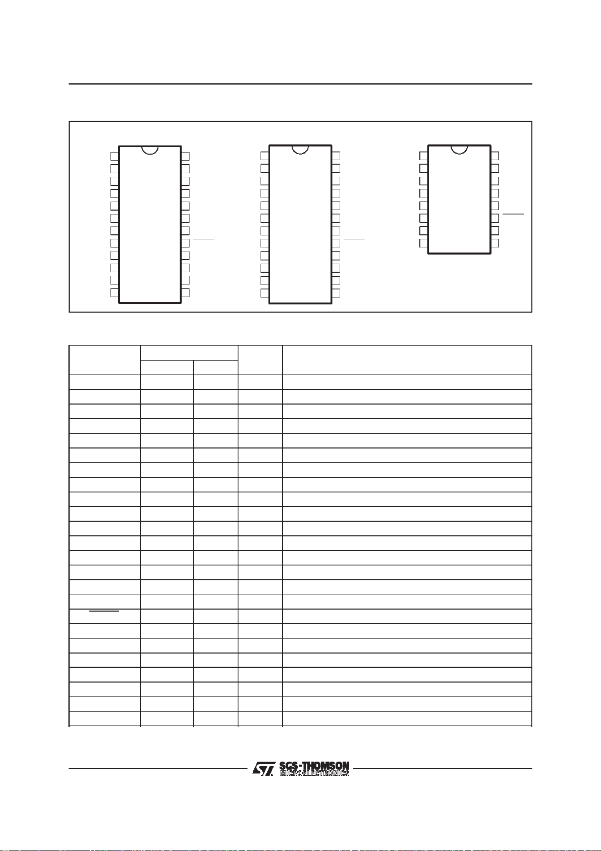
PIN CONNECTIONS
PWM0
PWM1
FBLK
VSYNC
HSYNC
V
PXCK
CKOUT
XTAL OUT
XTAL IN
PWM2
SDIP24 (STV9425)
1
2
3
4
5
6
DD
7
8
9
10
11
12
RES E RVED
PWM7
24
PWM6
23
TEST
22
B
21
G
20
R
19
GND
18
RESET
17
SDA
16
SCL
15
PWM5
14
PWM4PWM3
13
XTALOUT
SDIP24 (STV9425B)
1
PWM1
FBLK
VSYNC
HSYNC
PXCK
CKOUT
XTALIN
PWM2
2
3
4
5
V
6
DD
7
8
9
10
11
12
24
23
22
21
20
19
18
17
16
15
14
13
RESERVED
PWM6
TEST
B
G
R
GND
RESET
SDA
SCL
PWM5
RESERVEDRES E RVED
V-SYNC
H-SYNC
CKOUT
XTAL OUT
XTAL IN
PIN DESCRIPTION
Symbol
PWM0 1 * - O DAC0 Output
PWM1 2 - O DAC1 Output
FBLK 3 1 O Fast Blanking Output
V-SYNC 4 2 I Vertical Sync Input
H-SYNC 5 3 I HorizontalSync Input
V
DD
PXCK 7 5 O Pixel FrequencyOutput
CKOUT 8 6 O Clock Output
XTAL OUT 9 7 O Crystal Output
XTAL IN 10 8 I Crystal or Clock Input
PWM2 11 - O DAC2 Output
PWM3 12 * - O DAC3 Output
PWM4 13 * - O DAC4 Output
PWM5 14 - O DAC5 Output
SCL 15 9 I Serial Clock
SDA 16 10 I/O Serial Input/Output Data
RESET 17 11 I Reset Input (Active Low)
GND 18 12 S Ground
R 19 13 O Red Output
G 20 14 O Green Output
B 21 15 O Blue Output
TEST 22 16 I Reserved (grounded in NormalOperation)
PWM6 23 - O DAC6 Output
PWM7 24 * - O DAC7 Output
* Reserved with STV9425B(not to be connected)
Pin Number
I/O Description
SDIP24 DIP16
6 4 S +5V Supply
DIP16 (STV9426)
FBLK
PXCK
1
2
3
V
4
DD
5
6
7
8
TEST
16
B
15
G
14
R
13
GND
12
RESET
11
SDA
10
SCL
9
9425-01.EPS /9425B-01.EPS/9426-01.EPS
9425-01.TBL
2/15
Page 3
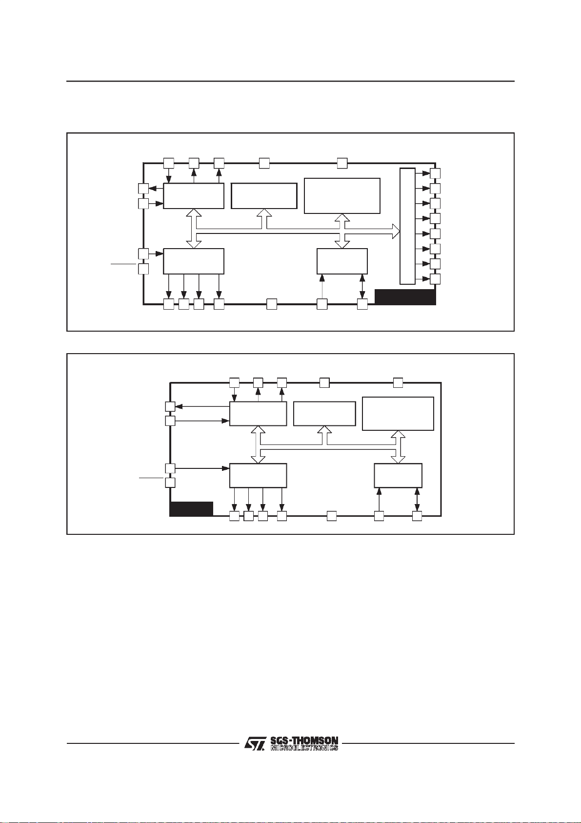
BLOCKDIAGRAMS
STV9425
STV9425 - STV9425B - STV9426
STV9426
CKOUT
HSYNC
VSYNC
RESET
XTALINXTAL
OUT PXCK TEST
V
DD
10 9 7 6 22
8
5
HORIZONTAL
DIGITAL PLL
4K ROM
(128 characters)
Address/Data
4
17
DISPLAY
CONTROLLER
19 20 21 3 18 15 16
R G B FBLK GND SCL SDA
XTALINXTAL
OUT PXCK TEST
78
CKOUT
HSYNC
6
3
HOR IZONTAL
DIGITALP LL
(128 characte rs)
1K RAM
Pa ge Descriptors +
User Defined Char.
2
I C BUS
INTERFACE
V
DD
45
4KRO M
PWM
STV9425/25B
*Reserved with STV9425B
16
1KRAM
Page Des criptors +
User Defined Char.
24
23
14
13
12
11
2
1
PWM7 *
PWM6
PWM5
PWM4 *
PWM3 *
PWM2
PWM1
PWM0 *
9425-02.EPS
VSYNC
RESET
2
11
STV9426
Addres s/Data
DISP LAY
CONTROLLER
1
R G B FBLK GND SCL
1213 14 15
INTERFACE
910
2
I C BUS
SDA
9426-02.EPS
3/15
Page 4
STV9425 - STV9425B - STV9426
ABSOLUTEMAXIMUM RATINGS
Symbol Parameter Value Unit
V
DD
V
IN
T
oper
T
stg
ELECTRICAL CHARACTERISTICS
=5V,VSS=0V,TA= 0 to70°C, F
(V
DD
Symbol Parameter Min. Typ. Max. Unit
SUPPLY
V
DD
I
DD
INPUTS
SCL, SDA, TEST, RESET, V-SYNC and H-SYNC
V
IL
V
IH
I
IL
OUTPUTS
R, G,B, FBLK, SDA, CKOUT, PXCK and PWMi (i = 0 to 7)
V
OL
V
OH
For R, G, B and FBLKoutputs, see Figure1.
Supply Voltage -0.3, +7.0 V
Input Voltage -0.3, +7.0 V
Operating AmbientTemperature 0, +70 °C
Storage Temperature -40, +125 °C
= 8 to15MHz, TEST= 0 V,unlessotherwise specified)
XTAL
Supply Voltage 4.75 5 5.25 V
Supply Current - 50 70 mA
Input Low Voltage 0.8 V
Input High Voltage 0.8V
DD
Input Leakage Current -20 +20
Output Low Voltage (IOL= 1.6mA) 0 0.4 V
Output High Voltage (IOL= -0.1mA) 0.8V
DD
V
DD
9425-02.TBL
V
A
µ
V
9425-03.TBL
Figure1 : TypicalR, G, B OutputsCharacteristics
V
(V)
,
V
OH
V
OL
I (A)
10
-4
10
-3
10
-2
10
-1
5
2.5
0
10
V
-5
OL OH
9425-17.EPS
4/15
Page 5
STV9425 - STV9425B - STV9426
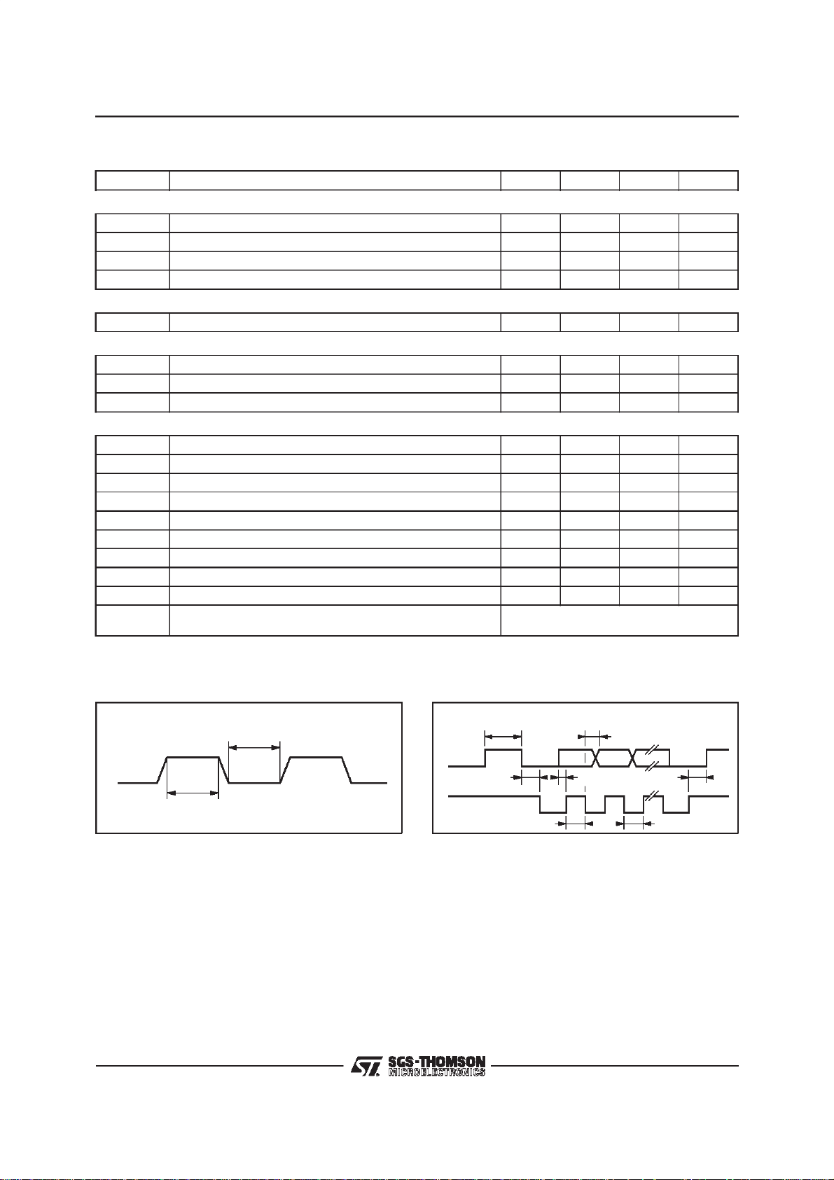
TIMINGS
Symbol Parameter Min. Typ. Max. Unit
OSCILATOR INPUT :XTI (see Figure 2)
T
WH
T
WL
F
XTAL
F
PXL
RESET
T
RES
R, G, B, FBLK (C
T
RISE
T
FALL
T
SKEW
I2C INTERFACE : SDA ANDSCL (see Figure 3)
F
SCL
T
BUF
T
HDS
T
SUP
T
LOW
T
HIGH
T
HDAT
T
SUDAT
T
F
T
R
Note 1 : These parameters are not tested on each unit. They are measured during our internal qualification procedure which includes
Clock High Level 20 ns
Clock Low Level 20 ns
Clock Frequency TBD 15 MHz
Pixel Frequency 50 MHz
Reset Low LevelPulse 4 µs
= 30pF)
LOAD
Rise Time (Note1) 5 ns
Fall Time (Note 1) 5 ns
Skew between R, G, B, FBLK (Note 1) 5 ns
SCL Clock Frequency 0 1 MHz
Time thebus must be free between 2 access 500 ns
Hold Timefor Start Condition 500 ns
Set upTime for StopCondition 500 ns
The Low Period of Clock 400 ns
The HighPeriod of Clock 400 ns
Hold TimeData 0 ns
Set upTime Data 375 ns
Fall Time of SDA 20 ns
Rise Time ofBoth SCL and SDA
characterization on batches comming from corners of our processes and also temperature characterization.
Depend onthe pull-up resistor
and the load capacitance
9425-04.TBL
Figure2
XTI
TWH
TWL
Figure3
9425-03.AI
STOP START DATA STOP
T
SDA
SCL
BUF
T
HDS
T
HIGH
T
SUDAT
T
HDAT
T
SUP
T
LOW
9425-04.AI
5/15
Page 6

STV9425 - STV9425B - STV9426
FUNCTIONAL DESCRIPTION
TheSTV9425/25B/26display processoroperation
iscontrolledby a host MCU viathe I
is fully programmable through 16 internal
read/write registers and performs all the display
functionsby generating pixels from data stored in
its internal memory. After the page downloading
from the MCU, the STV9425/25B/26 refreshes
screen by its built in processor, without any MCU
control (access).In addition, the host MCU has a
direct access to the on chip 1Kbytes RAM during
thedisplay of thecurrentpage tomakeanyupdate
of its contents.
WiththeSTV9425/25B/26,apagedisplayedonthe
screenis madeof severalstrips whichcan be of 2
types : spacing or character and which are described by a table of descriptors and character
codesin RAM. Severalpages can be downloaded
atthesame timein theRAM and the choice of the
currentdisplay page is made by programmingthe
CONTROL register.
I - Serial Interface
The 2-wires serial interface is an I
beconnectedto theI
2
C bus,a devicemustownits
slave address ; the slave address of the
STV9425/25B/26is BA(in hexadecimal).
A6 A5 A4 A3 A2 A1 A0 R/W
Figure3 : STV9425/25B/26/I2C WriteOperation
2
C interface.It
2
C interface.To
1011101
I.1 - Data Transferin WriteMode
The host MCU can write data into the
STV9425/25B/26registers orRAM.
To write data into the STV9425/25B/26, after a
start, the MCU must send (Figure 3) :
- First, theI
2
C address slave byte witha low level
for the R/W bit,
- The two bytes of the internal address where the
MCU wantsto writedata(s),
- The successivebytes of data(s).
All bytes are sent MS bit first and the write data
transferis closedby a stop.
I.2 - Data Transferin Read Mode
The host MCU can read data from the
STV9425/25B/26registers, RAM or ROM.
Toreaddata fromthe STV9425/25B/26(Figure 4),
theMCUmustsend2 differentI
firstoneismade ofI
2
CslaveaddressbytewithR/W
2
Csequences.The
bit at low level andthe 2 internaladdressbytes.
Thesecond one ismade of I
2
C slaveaddressbyte
with R/W bit at high level and all the successive
data bytes read at successive addresses starting
fromtheinitial addressgivenbythe firstsequence.
SCL
R/W
SDA
I2C Slave Address
SCL
D7 D6 D5 D4 D3 D2 D1 D0 D7 D6 D5 D4 D3 D2 D1 D0 D7 D6 D5 D4 D3 D2 D1 D0
SDA
ACK ACKData Byte 1 Data Byte 2 ACK Data Byte n Stop
A7 A6 A5 A4 A3 A2 A1 A0 - - A13 A12 A11 A10 A9 A8
ACK LSB Address ACK MSB Address ACKStart
Figure4 : STV9425/25B/26/I2C ReadOperation
SCL
SDA
I1C SlaveAddress
SCL
SDA R/W
I1CSlaveAddress
6/15
R/W
A7 A6 A5
ACK LSB Address ACK MSB Address ACKStart
D7 D6 D5 D4 D3 D2 D1 D0
ACK ACK Data Byte n ACKStart
A4 A3 A2 A1 A0
Data Byte 1
- - A13 A12 A10 A10 A9 A8
D7 D6 D5 D4 D3 D2 D1 D0
9425-05.AI
Stop
Stop
9425-06.EPS
Page 7

FUNCTIONAL DESCRIPTION(continued)
I.3 -AddressingSpace
STV9425/25B/26 registers, RAM and ROM are
mapped in a 16Kbytes addressing space. The
mappingis the following :
0000
03FF
0400
1FFF
2000
32FF
3300
3FFF
3FF0
3FFF
1024 bytesRAM
Empty Space
Character
Generator ROM
Empty Space
Internal
Registers
Descriptors character
codes user definable
characters
I.4 -Register Set
LINEDURATION
3FF0 VSP HSP LD5 LD4 LD3 LD2 LD1 LD0
* 0 0111111
VSP : V-SYNC activeedge selection
= 0 : falling egde,= 1 : risingedge
HSP : H-SYNCactive edge selection
= 0 : falling egde,= 1 : risingedge
LD[5:0] : LINE DURATION
(numberof pixel periodper linedivided
by 12 ie. Unit = 12 pixel periods).
HORIZONTAL DELAY
3FF1 DD7 DD6 DD5 DD4 DD3 DD2 DD1 DD0
*00001000
DD[7:0] : HORIZONTAL DISPLAY DELAY from
the H-SYNC reference falling edge to
st
the 1
pixel position of the character
strips.Unit = 3 pixel periods.
CHARACTERS HEIGHT
3FF2 - - CH5 CH4 CH3 CH2 CH1 CH0
*--010010
CH[5:0] : HEIGHT of the character strips in scan
lines.For eachscan line,the numberof
the slice whichis displayedis givenby :
SLICE-NUMBER=
SCAN−LINE−NUMBER x 18
round
CH[5:0]
.
SCAN-LINE-NUMBER= Numberof the
currentscan line of the strip.
STV9425 - STV9425B - STV9426
DISPLAYCONTROL
3FF3 OSD FBK FL1 FL0 - P8 P7 P6
*0000-000
OSD : ON/OFF(if0,R,G,B andFBLKare0).
FBK : Fast blankingcontrol :
=1:FBLK=1,forcingblackwherethese
is no display,
=0:FBLKisactiveonlyduringcharacter
display.
FL[1:0] : Flashing mode :
- 0 0 : No fl ashin g. Th e c har acter
attributeis ignored,
- 01 :1/1 flashing (a dutycycle = 50%),
- 10 : 1/3 flashing,
- 11: 3/1 flashing.
P[8:6] : Address of the 1
current displayed pages.
P[13:9] and P[5:0] = 0 ; upto 8 different
pages can be storedin theRAM.
LOCKINGCONDITIONTIME CONSTANT
3FF4 FR AS2 AS1 AS0 - BS2 BS1 BS0
*0010-010
FR : FreeRunning; if= 1 PLLis disabledand
the pixelfrequencykeeps its last value.
AS[2:0] : Phase constant during locking
conditions.
BS[2:0] : Frequency constant during locking
conditions.
CAPTUREPROCESSTIME CONSTANT
3FF5 - AF2 AF1 AF0 - BF2 BF1 BF0
*-011-011
AF[2:0] : Phase constant during the capture
process.
BF[2:0] : Frequency constant during the capture
process.
INITIALPIXELPERIOD
3FF6 PP7 PP6 PP5 PP4 PP3 PP2 PP1 PP0
*00101000
PP[7:0] : Value to initializethe pixel periodof the
PLL.
FREQUENCYMULTIPLIER
3FF7 - - - - FM3 FM2 FM1 FM0
* ----1010
FM[3:0] : Frequency multiplier of the crystal
frequency to reach the high frequency
used by the PLL to derive the pixel
frequency.
st
descriptor of the
7/15
Page 8

STV9425 - STV9425B - STV9426
FUNCTIONAL DESCRIPTION(continued)
PULSEWIDTH MODULATOR0
3FF8 V07 V06 V05 V04 V03 V02 V01 V00
* 00000000
V0[7:0] : Digital value of the 1stPWM D to A
converter(Pin1).
PULSEWIDTH MODULATOR1
3FF9 V17 V16 V15 V14 V13 V12 V11 V10
* 00000000
V1[7:0] : Digitalvalueof the2ndPWMDAC(Pin2).
PULSEWIDTH MODULATOR2
3FFA V27 V26 V25 V24 V23 V22 V21 V20
* 00000000
V2[7:0] : Digital value of the 3rdPWM DAC
(Pin11).
PULSEWIDTH MODULATOR3
3FFB V37 V36 V35 V34 V33 V32 V31 V30
* 00000000
V3[7:0] : Digital value of the 4thPWM DAC
(Pin12).
PULSEWIDTH MODULATOR4
3FFC V47 V46 V45 V44 V43 V42 V41 V40
* 00000000
V4[7:0] : Digital value of the 5thPWM DAC
(Pin13).
PULSEWIDTH MODULATOR5
3FFD V57 V56 V55 V54 V53 V52 V51 V50
* 00000000
V5[7:0] : Digital value of the 6thPWM DAC
(Pin14).
PULSEWIDTH MODULATOR6
3FFE V67 V66 V65 V64 V63 V62 V61 V60
* 00000000
V6[7:0] : Digital value of the 7thPWM DAC
(Pin23).
PULSEWIDTH MODULATOR7
3FFF V77 V76 V75 V74 V73 V72 V71 V70
* 00000000
V7[7:0] : Digital value of the 8thPWM DAC
(Pin24).
Note : * ispower on reset value.
II - Descriptors
SPACING
MSB0-------
LSB SL7 SL6 SL5 SL4 SL3 SL2 SL1 SL0
SL[7:0] : The number of the scan lines of the
spacingstrip (1 to 255).
CHARACTER
MSB 1 DE - ZY - - C9 C8
LSB C7 C6 C5 C4 C3 C2 C1 0
C[9:0] : Theaddress of the firstcharacter codeof
the strip (even).
DE : Displayenable :
- DE = 0, R = G = B = 0 and FBLK= FBK
(displaycontrol register) on whole strip,
- DE = 1, displayof the characters.
ZY : Zoom, ZY = 1 all the scan lines are
repeatedonce.
III - CodeFormat
MSB SET CHARACTER NUMBER
LSB BK3 BK2 BK1 BK0 FL RF GF BF
SET : The setCHARACTERNUMBER
- If SET= 0 : ROMcharacter,
- If SET= 1 :
• If CHARACTER NUMBER is 0 to
25, a user redefinable character
(UDC) located in RAM at the
address equal to :
38 x CHARACTER NUMBER,
• If CHARACTER NUMBER is 26 to
63, spacecharacter,
• If CHARACTERNUMBER>63,end
of line.
FL : Flashing attribute (the flashingmode
is definedin the DISPLAYCONTROL
register).
RF, GF,BF: Foregroundcolor.
BK[3:0] : Background:
- If BK3 = 0, BK[2:0] = background
color R, G and B,
- If BK3= 1, shadowing:
BK1 : horizontal shadowing.
(if BK1 = 0, the background is
transparent).
BK2 and BK0 must be equal to 0.
8/15
Page 9

FUNCTIONAL DESCRIPTION(continued)
Figure5 : HorizontalTiming
H-SYNC
R, G, B
STV9425 - STV9425B - STV9426
Character
Period
LD[5:0]
Fixed
DD[7:0]
Given by number
of characters of the strips
0123n+1n+2n+3n+4 LD-1LD01
= 4 (min) = 4n + 2
IV- Clock and Timing
The whole timing is derived from the XTALIN and
the SYNCHRO (horizontal and vertival) input frequencies. The XTALINinput frequency can be an
external clock or a crystal signal thanks to
XTALIN/XTALOUT pins. The value of this frequencycanbe chosenbetween 8 and 15MHz,it is
availableontheCKOUTpin andisusedbythePLL
to generate a pixel clock locked on the horizontal
synchroinput signal.
IV.1 - HorizontalTiming (seeFigure 5)
The number of pixel periods is given by the LINE
DURATIONregisterand is equalto :
[LD[5:0]+ 1 ] x 12.
(LD[5:0]: valueof the LINE DURATION register).
This value allows to choose the horizontal size of
the characters.The horizontal left margin is given
by the HORIZONTAL DELAYregister and is equal
to :
[DD[7:0]+ 8] x 3 x T
PXCK
(DD[7:0] : value of the DISPLAY DELAY register
andT
: pixel period).
PXCK
Thisvalue allows to choosethe horizontalposition
of the characters on the screen. The value of
DD[7:0]must be equal or greaterthan4 (theminimumvalueof thehorizontaldelayis 36xT
PXCK
=3
character periods). The length of the active area,
whereR,G, Bare differentfrom 0, dependson the
numberof charactersof the strips.
IV.2 - D to ATiming
TheD to Aconvertersof the STV9425/25B/26are
pulsewidth modulater converter.The frequencyof
F
the output signal is :
and the duty cycleis :
XTAL
256
Vi[7:0]
256
per cent.
After a low pass filter, the average value of the
output is :
Vi
256
⋅ V
DD
[7:0]
V - DisplayControl
Ascreeniscomposedofsuccessivescanlinesgathered in several strips. Each strip is defined by a
descriptorstored in memory. A table of descriptors
allowsscreencomposition and different tablescan
bestoredin memoryat thepageaddresses(8possible≠addresses).Twotypesofstripsareavailable :
- Spacing strip : its descriptor (see II) gives the
numberof black(FBK= 1inDISPLAYCONTROL
register)or transparent(FBK= 0) lines.
- Character strip : its descriptor gives the memory
addressof thecharactercodescorrespondingto
st
the 1
displayed character.The characters and
attributes (see code format III) are defined by a
succession of codes stored in the RAM at addresses starting from the 1
st
one given by the
descriptor.A character strip can be displayed or
not by using the DE bit of its descriptor.A zoom
can bemade on it byusing the ZYbit.
Figure 6 : PWMTiming
V1[7:0]
128
255
PWM1 Signal
0
1
T
XTAL
256.T
XTAL
9425-07.AI
9425-08.AI
9/15
Page 10

STV9425 - STV9425B - STV9426
FUNCTIONAL DESCRIPTION(continued)
After the falling edge on V-SYNC, the first strip
descriptoris read at the top of thecurrent tableof
descriptors at the address given by P[9:0] (see
DISPLAYCONTROL register).I
f it is a spacing strip, SL[7:0] black or transparent
scanlines are displayed.
If it is a characterstrip, during CH[5:0] x (I + ZY)
Figure7 :
Relation between Screen/AddressPage/CharacterCode in RAM
DISP LAYCONTROL Register
CS D FBK FL[1:0] P8 P7 P 8
scan lines (CH[5:0] given by the CHARACTER
HEIGHTregister), thecharacter codes arereadat
theaddressesstartingfromthe 1
st
onegivenby the
descriptoruntil aendofline characteror the end of
the scanline.
The next descriptor is then read and the same
process is repeated until the next falling edge on
V-SYNC.
V-SYNC
2nd CHARACTER
STRIP CODES
OTHER
TABLE OF
DESCRIPTORS
OTHER
(UDC for example)
1st CHARACTER
STRIP CODES
3rd CHARACTER
SRTIP CODES
OTHER
(CODES OR
DESCRIPTORS)
RAM CODE
AND DES CRIPTORS
Figure8 : UserDefinable Character
ON THE SCREEN
36 Pixels (= 3 Characters)
123
36 Slices (= 2 Characters)
456
SPACING
ROW1
ROW2
SPACING
ROW3
SPACING
TABLE OF THE
DESCRIPTORS
Character Number
1
2
3
4
5
6
7
8
9
10
11
12
13
14
15
16
17
18
1
2
3
4
5
6
7
8
9
10
11
12
13
14
15
16
17
18
Character Number
TOP SPACING STRIP
1s t CHARACTER STRIP
2nd CHARACTER S TRIP
SPACING STRIP
3rd CHARACTER STRIP
|
BOTTOM SPACING STRIP
SCREEN
IN THE RAM
(example for Character n°5)
Slice 0
Slice 1
Slice 2
Slice 3
Slice 4
Slice 5
Slice 6
Slice 7
Slice 8
Slice 9
Slice 10
Slice 11
Slice 12
Slice 13
Slice 14
Slice 15
Slice 16
Slice 17
Slice 18
: 0x01
: 0x00
: 0x08
: 0x0c
: 0x0e
: 0x0f
: 0x0f
: 0x0f
: 0x0f
: 0x0e
: 0x0c
: 0x00
: 0x00
: 0x00
: 0x00
: 0x00
: 0x00
: 0x00
: 0x00
Odd
Address
0xff =
Slice 18 of the character n°2
only for vertical shadowing
(not displayed).
0xff
0x7f
0x3f
0x1f
0x1f
0x1f
0x1e
0x1e
0x3c
0x3c
0x78
0x78
0xf1
0x00
0x00
0x00
0x00
0x00
Even
Address
9425-09.EPS
9425-10.AI
10/15
Page 11

FUNCTIONAL DESCRIPTION(continued)
Table1 : ROM CharacterGenerator
CHARACTER NUMBER C(6:0)
C(6:4)
01234567
C(3:0)
0
1
2
3
4
5
STV9425 - STV9425B - STV9426
6
7
8
9
a
b
c
d
e
f
9425-11.EPS
11/15
Page 12

STV9425 - STV9425B - STV9426
FUNCTIONAL DESCRIPTION(continued)
VI- User DefinableCharacter
The STV9425/25B/26 allows the user to dynamically define character(s) for his own needs (for a
specialLOGO for example). Like theROM characters, a UDC is madeof a 12 pixels x 18 slices dot
matrix,but one more slice is added for thevertical
shadowing when several UDCs are gathered to
makea specialgreat character (see Figure8).
In a UDC, each pixel is definedwith a bit, 1 refers
to foreground, and 0 to background color. Each
sliceof a UDC uses 2 bytes:
add +1- - - - PX11 PX10 PX9 PX8
add
(even)
PX11is theleftmostpixel.Characterslice address:
SLICEADDRESS=38x(CHARACTERNUMBER)
+(SLICE NUMBER).
Where:
- CHARACTER NUMBER is the number given by
the charactercode,
- SLICENUMBERis the numbergiven by theslice
interpolator (n° of the current slice of the strip :
1 < <18)
VII - ROM Character Generator
The STV9425/25B/26includes a ROM character
generator which is made of 128 alphanumeric or
graphiccharacters(see Table1)
VIII - PLL
ThePLLfunctionof theSTV9425/25B/26provides
the internal pixel clock locked on the horizontal
synchrosignal and used by the displayprocessor
togenerate the R, G,B and fast blanckingsignals.
It is made of 2 PLLs. The first one analogic
(see Figure 9), provides a high frequency signal
locked on the crystal frequency. The frequency
multiplieris givenby :
N=2⋅(FM[3:0]+ 3)
Where FM[3:0] is the value of the FREQUENCY
MULTIPLIERregister.
Figure9 : AnalogicPLL
PX7 PX6 PX5 PX4 PX3 PX2 PX1 PX0
N.F
XTAL
VCO
%N F
FILTRE
XTAL
The second PLL, full digital (see Figure 10), provides a pixel frequency locked on the horizontal
synchrosignal. Theratio betweenthe frequencies
of these 2 signalsis :
M = 12 x (LD[5:0]+ 1)
WhereLD[5:0] is thevalueofthe LINEDURATION
register.
XTAL
Digital PLL
%D
M.F
H-SYNC
%M F
ALGO
err(n)D(n)
Figure 10 :
N.F
VIII.1 - Programmingof the PLL Registers
FrequencyMultiplier
(@3FF7)
This register gives the ratio between the crystal
frequency and the high frequency of the signal
usedbythe2
nd
PLLtoprovide,bydivision,thepixel
clock. The value of this high frequency must be
near to 200MHz (for example if the crystal is a
8MHz, the value of FM must be equal to 10) and
greaterthan 6 x (pixelfrequency).
Initial Pixel Period
(@3FF6)
This register allows to increase the speed of the
convergence of the PLL when the horizontal frequencychanges (new graphic standart).The relationshipbetweenFM[3:0],PP[7:0],LD[5:0],F
and F
PP[7:0] = round
LockingCondition Time Constant
XTAL
is:
2
⋅(FM[3:0]+ 3) ⋅ F
8 ⋅
12
⋅ (
LD[5:0]+1
XTAL
F
) ⋅
HSYNC
(@ 3FF4)
This register gives the constants AS[2:0] and
BS[2:0]usedby thealgo partof thePLL(seeFigure
10) to calculate, from the phase error, err(n), the
new value, D(n), of the division of the high frequencysignaltoprovidethe pixelclock.Thesetwo
constantsare usedonlyin lockingcondition, which
is true,if the phaseerror is less than a fixedvalue
during at least, 4 scan lines. If the phase error
becomes greater than the fixed value, the PLL is
not in locking condition but in capture process. In
this case, the algo part of the PLLused the other
constants,AF[2:0] and BF[2:0], given by the next
register.
CaptureProcess Time Constant
(@ 3FF5)
The choice between these two time constants
(locking condition or capture process) allows to
decreasethecaptureprocesstimebychangingthe
time response of the PLL.
9425-12.AI
H-SYNC
HSYNC
− 24
9425-13.AI
12/15
Page 13

FUNCTIONAL DESCRIPTION(continued)
VIII.2 - How to choosethe value of the time
constant?
The time response of the PLL is given byits characteristicequation whichis :
2
(x − 1)
+(α
+
β
)⋅(x−
1
)
+
β=
0
.
Where:
α=3⋅LD[5:0] ⋅ 2
A − 11
and β=3⋅LD[5:0]⋅ 2
B − 19
(LD[5:0] = value of the LINE DURATION register,
A = value of the 1st time constant, AF or AS and
B = value of the2
d
time constant,BF or BS).
As you can see, the solution depend only on the
LINE DURATION and the TIME CONSTANTS
given by the I
If (α + β)
2
C registers.
2
− 4β ≥ 0 and 2α−β<4, thePLL is sta-
ble and its response is like this presented on
Figure11.
Figure11 :
Time Response of the PLL/CharacteristicEquation Solutions(with
Real Solutions)
PLL
Frequency
f
1
If (α + β)
f
0
Input
Frequency
f
1
f
0
2
− 4β ≤ 0, theresponse of the PLL is like
t
t
thispresented onFigure 12.
STV9425 - STV9425B - STV9426
In this case the PLL is stable if τ > 0.7 damping
coefficient).
Figure 12 : Time Responseof the PLL/Charac-
teristic Equation Solutions (with
ComplexSolutions)
PLL
.
9425-14.AI
Frequency
f
1
f
0
Input
Frequency
f
1
f
0
The Table 2 gives some good values for A and B
constants for different values of the LINE DURATION.
Summary
For a goodworkingof the PLL:
- A and B time constantsmust be chosen among
valuesfor which the PLLis stable,
- B mustbe equal or greaterthan Aand the difference betweenthem must be lessthan 3,
- The greater(A, B) are, the fasterthe captureis.
Anoptimalchoiceforthemostofapplicationsmight
be :
- For locking condition: AS = 0 and BS = 1,
- For capture process : AS = 2 and BS= 4.
But for each application the time constantscan be
calculated by solving the characteristic equation
and choosingthe bestresponse.
t
t
9425-15.AI
Table2 : ValidTime Constants Examples
B\A0123456
0
1 YYYY YYYY YYYY YYYN YNNN NNNN NNNN
2 NYYY YYYY YYYY YYYN YNNN NNNN NNNN
3
4 NNNN NYYY
5 NNNN NNNY YYYY YYYN YNNN NNNN NNNN
6
7 NNNN NNNN NNNY YYYN YNNN NNNN NNNN
Note : 1. Case ofA[2:0]= 1 (001) and B[2:0] = 4 (100) :
LD
Valid Time Constants
YYYY YYYY YYYY YYYN YNNN NNNN NNNN
NNNY YYYY YYYY YYYN YNNN NNNN NNNN
NNNN NNNN NYYY YYYN YNNN NNNN NNNN
16 32 48 63
NYYY
(1)
YYYY YYYN YNNN NNNN NNNN
Valueof LINEDURATION Register (@ 3FF0) :
LD = 16: LD[5:0] = 010000
LD = 32: LD[5:0] = 100000
LD = 48: LD[5:0] = 110000
LD = 63: LD[5:0] = 111111
Tablemeaning :
N = No possible capture
Y = PLL can lock
13/15
9425-05.TBL
Page 14

STV9425 - STV9425B - STV9426
PACKAGE MECHANICAL DATA (STV9425- STV9425B)
24 PINS- PLASTICSHRINK DIP
BeB1
D
A1
Stand-off
A2
E
E1
LA
e1
e2
c
E
13
F
12
SDIP24
e3
e2
.015
0,38
Gage Plane
Dimensions
24
1
Millimeters Inches
Min. Typ. Max. Min. Typ. Max.
A 5.08 0.20
A1 0.51 0.020
3.05 3.30 4.57 0.120 0.130 0.180
B 0.36 0.46 0.56 0.0142 0.0181 0.0220
B1 0.76 1.02 1.14 0.030 0.040 0.045
C 0.23 0.25 0.38 0.0090 0.0098 0.0150
D 22.61 22.86 23.11 0.890 0.90 0.910
E 7.62 8.64 0.30 0.340
E1 6.10 6.40 6.86 0.240 0.252 0270
e 1.778 0.070
e1 7.62 0.30
e2 10.92 0.430
e3 1.52 0.060
L 2.54 3.30 3.81 0.10 0.130 0.150
PMSDIP24.EPS
SDIP24.TBL
14/15
Page 15

PACKAGE MECHANICAL DATA (STV9426)
16 PINS- PLASTICDIP
STV9425 - STV9425B - STV9426
PM-DIP16.EPS
Dimensions
Min. Typ. Max. Min. Typ. Max.
Millimeters Inches
a1 0.51 0.020
B 0.77 1.65 0.030 0.065
b 0.5 0.020
b1 0.25 0.010
D 20 0.787
E 8.5 0.335
e 2.54 0.100
e3 17.78 0.700
F 7.1 0.280
I 5.1 0.201
L 3.3 0.130
Z 1.27 0.050
Informationfurnishedis believed to be accurateand reliable.However, SGS-THOMSONMicroelectronics assumes no responsibility
for theconsequences of use ofsuch information nor for any infringementof patentsor other rightsof thirdparties whichmay result
from itsuse. No licence isgrantedby implication orotherwise underany patentor patent rights of SGS-THOMSONMicroelectronics.
Specifications mentioned in this publication are subject to change without notice. This publication supersedes and replaces all
informationpreviouslysupplied.SGS-THOMSON Microelectronics products are not authorized for use as criticalcomponents inlife
support devices or systemswithout express written approval of SGS-THOMSON Microelectronics.
1997SGS-THOMSON Microelectronics - All Rights Reserved
2
Purchase of I
2
I
C Patent.Rights to use these components in a I2C system,is grantedprovided that the system conforms to
Australia - Brazil- Canada- China - France- Germany- Italy - Japan -Korea - Malaysia - Malta- Morocco
The Netherlands - Singapore - Spain - Sweden- Switzerland - Taiwan - Thailand- UnitedKingdom - U.S.A.
C Components of SGS-THOMSON Microelectronics, conveys a license under the Philips
2
C StandardSpecifications as defined by Philips.
the I
SGS-THOMSON Microelectronics GROUP OF COMPANIES
DIP16.TBL
15/15
 Loading...