

Page 1
MULTISYNCON-SCREENDISPLAY FOR MONITOR
.
CMOSSINGLECHIP OSDFOR MONITOR
.
BUILT IN 1 KBYTE RAM HOLDING:
- PAGES’DESCRIPTORS
- CHARACTER CODES
- USERDEFINABLECHARACTERS
.
128 ALPHANUMERIC CHARACTERS OR
GRAPHIC SYMBOLS IN INTERNAL ROM
(12 x 18 DOTMATRIX)
.
UP TO 26 USERDEFINABLECHARACTERS
.
INTERNALHORIZONTAL PLL(15 TO120kHz)
.
PROGRAMMABLE VERTICAL HEIGHT OF
CHARACTER WITH A SLICEINTERPOLATOR
TO MEET MULTI-SYNCH REQUIREMENTS
.
PROGRAMMABLE VERTICAL AND HORIZONTALPOSITIONING
.
FLEXIBLESCREENDESCRIPTION
.
CHARACTER BY CHARACTER COLOR SELECTION(UP TO 8 DIFFERENT COLORS)
.
PROGRAMMABLE BACKGROUND (COLOR,
TRANSPARENTOR WITH SHADOWING)
.
CHARACTER BLINKING
.
2-WIRES ASYNCHRONOUS SERIAL MCU
INTERFACE (I
.
4 x 8 BITS PWM DAC OUTPUTS ON THE
STV9421
.
SINGLEPOSITIVE5V SUPPLY
2
C PROTOCOL)
STV9420
STV9421
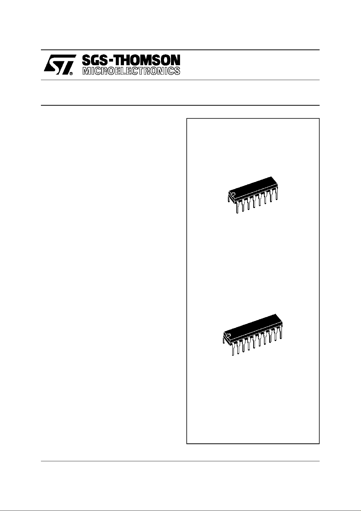
DIP16
(Plastic Package)
ORDER CODE : STV9420
DESCRIPTION
The STV9420/21is an ON SCREEN DISPLAYfor
monitor.It is built as a slaveperipheralconnected
to a host MCU via a serial I
display memory, controls all the display attributes
and generatespixels from the data read in its on
chip memory. The line PLL and a special slice
interpolator allow to have a display aspect which
doesnotdependonthelineandframefrequencies.
2
C interface allows MCU to make transparent in-
I
ternal accessto preparethe next pagesduring the
display of the current page. Toggle from one page
to anotherby programmingonly one register.
4 x 8 bits PWM DAC are available (STV9421) to
provide DC voltage control to other peripherals.
The STV9420/21providesthe user aneasy to use
and cost effective solutionto displayalphanumeric
or graphicinformation on monitor screen.
October 1995
2
C bus. It includes a
DIP20
(Plastic Package)
ORDER CODE : STV9421
1/16
Page 2
STV9420 - STV9421
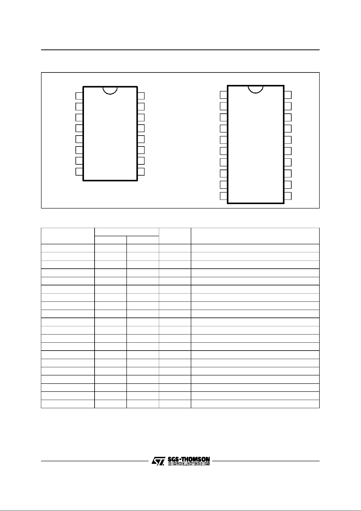
PINCONNECTIONS
DIP16
FBLK
H-SYNC
V-SYNC
V
DD
PXCK
CKOUT
XTALOUT
XTALIN
1
2
3
4
5
6
7
8
16
15
14
13
12
11
10
TEST
B
G
R
GND
RESET
SDA
9
SCL
PWM1
FBLK
H-SYNC
V-SYNC
PXCK
CKOUT
XTALOUT
XTALIN
PWM4
PIN DESCRIPTION
Symbol
PWM1 1 O DAC1 Output
FBLK 1 2 O Fast Blanking Output
H-SYNC 2 3 I Horizontal Sync Input
V-SYNC 3 4 I Vertical Sync Input
V
DD
PXCK 5 6 O PixelFrequency Output
CKOUT 6 7 O Clock Output
XTALOUT 7 8 O Crystal Output
XTALIN 8 9 I Crystal or Clock Input
PWM4 10 O DAC4 Output
PWM2 11 O DAC2 Output
SCL 9 12 I SerialClock
SDA 10 13 I/O SerialInput/output Data
RESET 11 14 I Reset Input
GND 12 15 S Ground
R 13 16 O Red Output
G 14 17 O Green Output
B 15 18 O Blue Output
TEST 16 19 I Reserved (grounded in Normal Operation)
PWM3 20 O DAC3 Output
Pin Number
DIP16 DIP20
I/O Description
4 5 S +5V Supply
DIP20
1
2
3
4
V
DD
5
6
7
8
9
10
20
19
18
17
16
15
14
13
12
11
PWM3
TEST
B
G
R
GND
RESET
SDA
SCL
PWM2
9420-01.AI /9421-01.AI
9420-01.TBL
2/16
Page 3
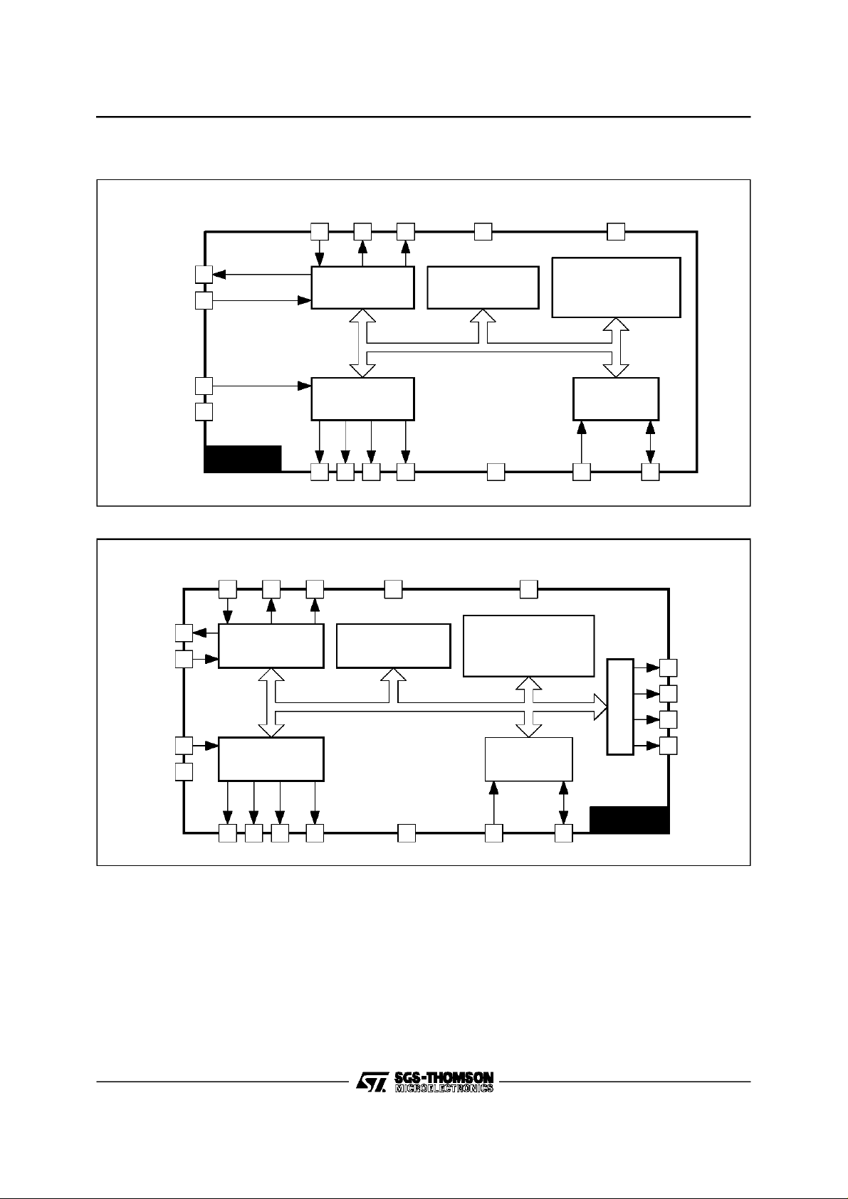
BLOCK DIAGRAMS
STV9420
XTALINXTAL
OUT
78
PXCK TES TV
DD
45
STV9420 - STV9421
16
STV9421
CKOUT
HSYNC
CKOUT
HSYNC
VSYNC
RESET
6
2
3
11
STV9420
XTALINXTAL
7
3
PXCK TEST
OUT
89
HORIZONTAL
DIGITAL PLL
Address/Data
HORIZONTAL
DIGITAL PLL
Addre ss/Data
DISPLAY
CONTROLLER
1
G B FBLK GND SCL
R
V
DD
56
4KROM
(128 characters)
4KROM
(128 characters)
1213 14 15
19
1K RAM
Page Descriptors +
User Defined Char.
1KRAM
Page Descriptors +
User Defined Char.
2
I C BUS
INTERFACE
910
SDA
10
20
9420-02.EPS
PWM4
PWM3
VSYNC
RESET
14
4
DISPLAY
CONTROLLER
2
1516 17 18
R G B FBLK GND SCL SDA
2
I C BUS
INTERFACE
12 13
PWM
STV9421
11
1
PWM2
PWM1
9421-02.EPS
3/16
Page 4
STV9420 - STV9421
ABSOLUTEMAXIMUM RATINGS
Symbol Parameter Value Unit
V
DD
V
IN
T
oper
T
stg
ELECTRICAL CHARACTERISTICS
=5V,VSS=0V,TA=0 to 70°C, F
(V
DD
Symbol Parameter Min. Typ. Max. Unit
SUPPLY
V
DD
I
DD
INPUTS
SCL, SDA, TEST, RESET, V-SYNC and H-SYNC
V
IL
V
IH
I
IL
OUTPUTS
R, G, B, FBLK, SDA, CKOUT, PXCK and PWMi(i = 1 to 4)
V
OL
V
OH
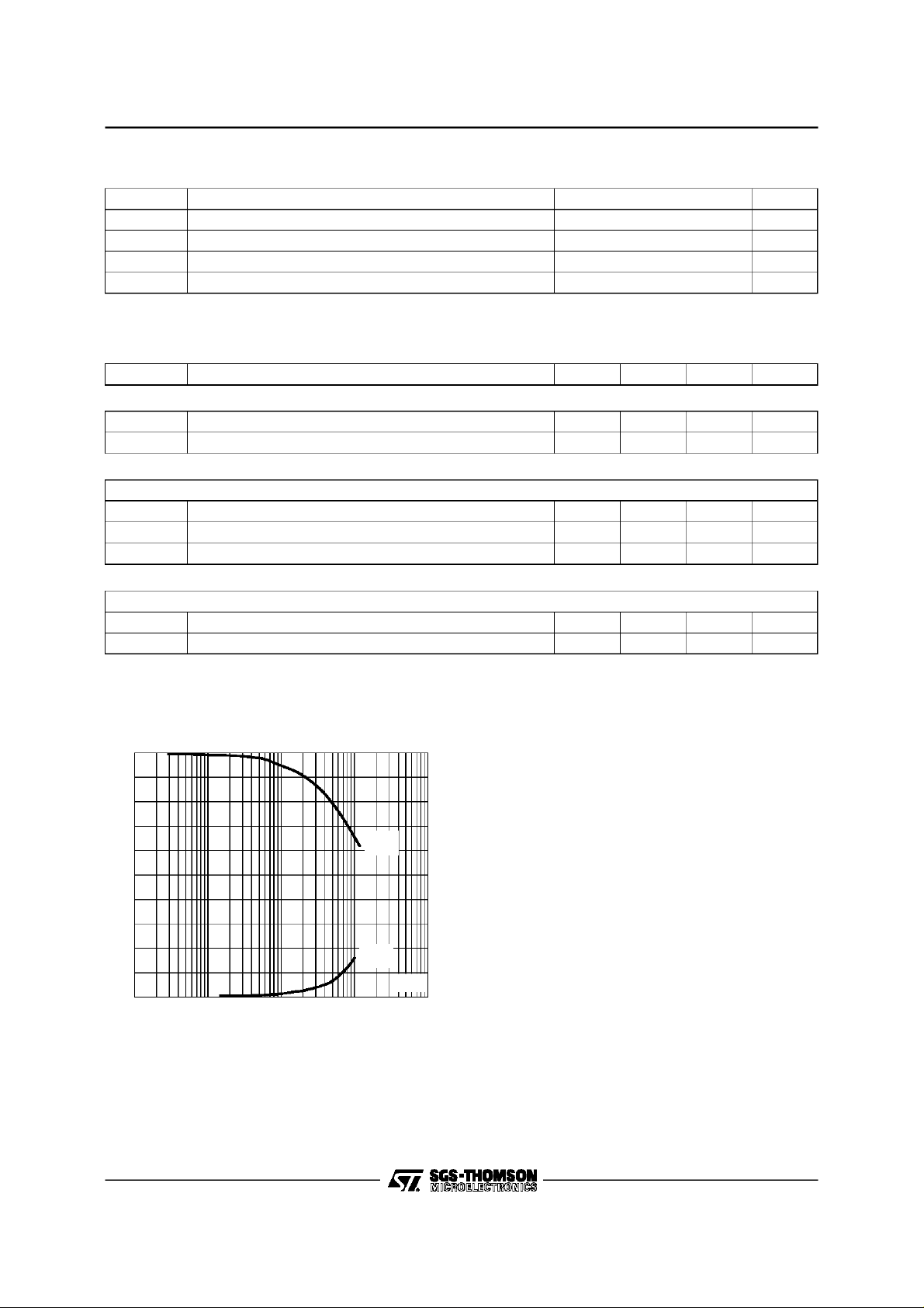
For R, G, B and FBLK outputs, see Figure 1.
Supply Voltage -0.3, +7.0 V
Input Voltage -0.3, +7.0 V
Operating Ambient Temperature 0, +70 °C
Storage Temperature -40, +125 °C
= 8 to15MHz, TEST= 0 V,unless otherwise specified)
XTAL
Supply Voltage 4.75 5 5.25 V
Supply Current - - 50 mA
Input Low Voltage 0.8 V
Input High Voltage 0.8 V
DD
Input Leakage Current -20 +20 µ
Output Low Voltage (IOL= 1.6mA) 0 0.4 V
Output High Voltage (IOL= -0.1mA) 0.8 V
DD
V
DD
9420-02.TBL
V
A
V
9420-03.TBL
Figure 1 : TypicalR, G, B OutputsCharacteristics
(V)
V
,
V
OH
V
OL
I (A)
10
-4
10
-3
10
-2
10
-1
5
2.5
0
V
10
OL OH
-5
9420-17.EPS
4/16
Page 5
STV9420 - STV9421
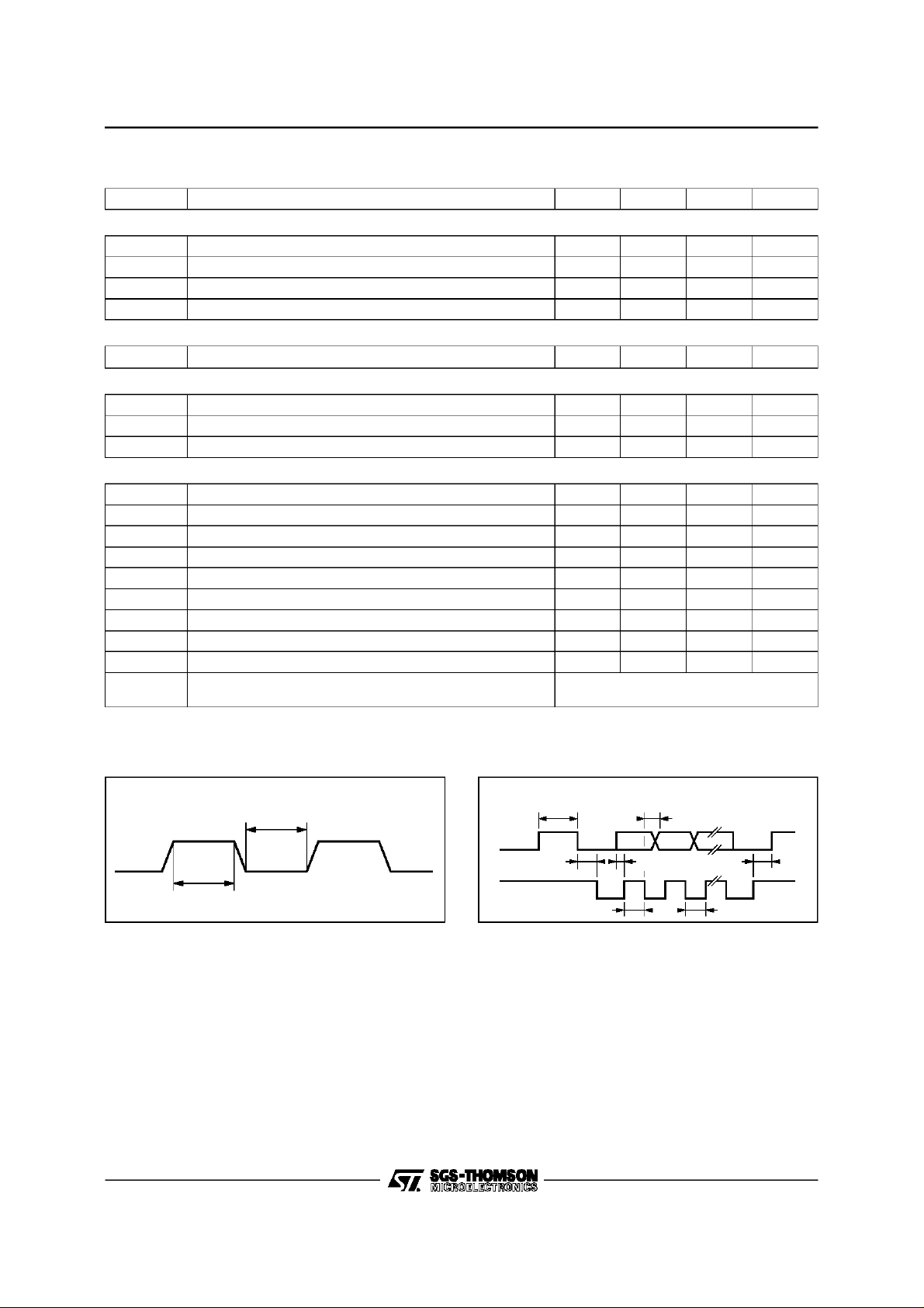
TIMINGS
Symbol Parameter Min. Typ. Max. Unit
OSCILATOR INPUT : XTI (see Figure 2)
t
WH
t
WL
f
XTAL
f
PXL
RESET
t
RES
R, G, B, FBLK (C
t
R
t
F
t
SKEW
2
I
C INTERFACE : SDA AND SCL (see Figure 3)
f
SCL
t
BUF
t
HDS
t
SUP
t
LOW
t
HIGH
t
HDAT
t
SUDAT
t
F
t
R
Note 1 : These parameters are not tested on each unit. They are measured during our internal qualification procedure which includes
Clock High Level 35 ns
Clock Low Level 35 ns
Clock Frequency 6 15 MHz
Pixel Frequency 30 MHz
Reset High Level Pulse 4
= 30pF)
LOAD
Rise Time (Note 1) 5 ns
Fall Time (Note 1) 5 ns
Skew between R, G, B, FBLK (Note 1) 5 ns
SCL Clock Frequency 0 1 MHz
Time the bus must be free between 2 access 500 ns
Hold Time for Start Condition 500 ns
Set up Time for Stop Condition 500 ns
The Low Period of Clock 400 ns
The High Period of Clock 400 ns
Hold Time Data 0 ns
Set up Time Data 375 ns
Fall Time of SDA 20 ns
Rise Time of Both SCL and SDA
characterization on batches comming from corners of our processes and also temperature characterization.
Depend on the pull-up resistor
and the load capacitance
µs
9420-04.TBL
Figure2
XTI
Figure 3
STOP START DATA STOP
t
t
WL
SDA
t
WH
SCL
9420-03.EPS
BUF
t
HDS
t
HIGH
t
S UDAT
t
HDAT
t
SUP
t
LOW
9420-04.EPS
5/16
Page 6

STV9420 - STV9421
FUNCTIONAL DESCRIPTION
The STV9420/21 display processor operation is
controlledby a host MCU via the I
fully programmable through 8 internal read/write
registers (12 for STV9421) and performs all the
display functions by generating pixels from data
stored in its internal memory. Afterthe page downloading from the MCU, the STV9420/21refreshes
screen by its built in processor, without any MCU
control (access).In addition, the host MCU has a
direct access to the on chip 1Kbytes RAM during
the displayof thecurrent page tomake anyupdate
of itscontents.
With the STV9420/21, a page displayed on the
screenis made of severalstrips which can be of 2
types : spacing or character and which are described by a table of descriptors and character
codes in RAM.Several pages can be downloaded
at thesame time in the RAMand the choiceof the
currentdisplay page is made by programmingthe
CONTROLregister.
I - Serial Interface
The 2-wires serial interface is an I
be connectedto theI
2
C bus,a devicemust own its
sl ave ad dre ss ; the sla ve a dd re ss of t he
STV9420/21is BA (in hexadecimal).
A6 A5 A4 A3 A2 A1 A0 R/W
1011101
Figure 3 : STV9420/I2C Write Operation
2
C interface.It is
2
C interface. To
I.1 - Data Transferin Write Mode
The hostMCU canwrite data into the STV9420/21
registersor RAM.
Towrite datainto theSTV9420/21,aftera start,the
MCUmust send(Figure 3) :
- First, the I
2
C address slave byte with a low level
for the R/W bit,
- The two bytes of the internal address where the
MCU wants to write data(s),
- The successive bytesof data(s).
All bytes are sent MS bit first and the write data
transferis closed by a stop.
I.2 - Data Transferin Read Mode
Thehost MCUcanreaddatafromthe STV9420/21
registers,RAM or ROM.
To read data from the STV9420/21(Figure 4), the
MCUmust send2 different I
Thefirst oneis madeof I
2
C sequences.
2
Cslaveaddressbytewith
R/W bit at low level and the 2 internal address
bytes.
2
The secondone ismade of I
C slave addressbyte
with R/W bit at high level and all the successive
data bytes read at successive addressesstarting
fromthe initialaddress givenby the first sequence.
SCL
R/W
SDA
2
C Slave Address
I
SCL
D7 D6 D5 D4 D3 D2 D1 D0 D7 D6 D5 D4 D3 D2 D1 D0 D7 D6 D5 D4 D3 D2 D1 D0
SDA
ACK ACKData Byte 1 Data Byte 2 ACK Data Byte n Stop
A7 A6 A5 A4 A3 A2 A1 A0 - - A13 A12 A11 A10 A9 A8
ACK LSB Address ACK MSB Address ACKStart
Figure 4 : STV9420/I2C Read Operation
SCL
R/W
SDA
I1C Slave Address
SCL
SDA R/W
I1C SlaveAddress
6/16
A7 A6 A5
ACK LSB Address ACK MSB Address ACKStart
D7 D6 D5 D4 D3 D2 D1 D0
ACK ACK Data Byte n ACKStart
A4 A3 A2 A1 A0
Data Byte 1
- - A13 A12 A10 A10 A9 A8
D7 D6 D5 D4 D3 D2 D1 D0
Stop
Stop
9420-05.AI
9420-06.EPS
Page 7

FUNCTIONAL DESCRIPTION (continued)
I.3 - Addressing Space
STV9420/21registers,RAMandROMare mapped
in a 16Kbytesaddressing space. The mapping is
the following:
0000
1024 bytes
RAM
03FF
Descriptorscharacter
codesuser definable
characters
0400
Empty
Space
1FFF
2000
Character
Generator
ROM
32FF
3300
Empty
Space
3FFF
3FF0
Internal
Registers
3FFF
I.4 - RegisterSet
LINE DURATION
3FF0 - - LD5 LD4 LD3 LD2 LD1 LD0
* --111111
LD[5:0] : LINE DURATION (number of character
period,1LSB =12 pixelperiods).
HORIZONTALDELAY
3FF1 DD7 DD6 DD5 DD4 DD3 DD2 DD1 DD0
* 00001000
DD[7:0] : HORIZONTAL DISPLAY DELAY from
the H-SYNC reference falling edge to
st
the 1
pixel position of the character
strips.
Unit = 3 pixel periods.
CHARACTERS HEIGHT
3FF2 - - CH5 CH4 CH3 CH2 CH1 CH0
* --010010
CH[5:0] : HEIGHT of the character strips in scan
lines.For each scan line, the number of
theslice which is displayedis given by:
SLICE-NUMBER =
SCAN±LINE±NUMBER x 18
round
SCAN-LINE-NUMBER = Number of the current scan
line of the strip.
CH[5:0]
STV9420 - STV9421
DISPLAYCONTROL
3FF3 OSD FBK FL1 FL0 - P8 P7 P6
* 0000-000
OSD : ON/OFF(i f0, R, G, B andFBLKare 0).
FBK : Fast blanking control :
= 1 : FBLK = 1, forcing black where
theseis no display,
=0:FBLKisactiveonlyduring
characterdisplay.
FL[1:0] : Flashing mode :
- 0 0 : No flash ing. T he chara cter
attributeis ignored,
- 01 : 1/1 flashing(a duty cycle = 50%),
- 10 : 1/3 flashing,
- 11: 3/1 flashing.
P[8:6] : Address of the 1
currentdisplayed pages.
P[13:9]and P[5:0] = 0 ; up to 8 different
pages can be stored in the RAM.
LOCKINGCONDITION TIME CONSTANT
3FF4 FR AS2 AS1 AS0 - BS2 BS1 BS0
* 0010-010
FR : FreeRunning; if=1PLLis disabledand
the pixel frequency keepsits last value.
AS[2:0] : Phase constant during locking
conditions.
BS[2:0] : Frequen cy constant during loc king
conditions.
CAPTUREPROCESSTIME CONSTANT
3FF5 - AF2 AF1 AF0 - BF2 BF1 BF0
* -011-011
AF[2:0] : Phase constant during the capture
process.
BF[2:0] : Frequencyconstant during the capture
process.
INITIALPIXELPERIOD
3FF6 PP7 PP6 PP5 PP4 PP3 PP2 PP1 PP0
* 00101000
PP[7:0] : Value to initialize the pixel period of the
PLL.
FREQUENCY MULTIPLIER
3FF7 - - - - FM3 FM2 FM1 FM0
*----1010
FM[3:0] : Frequency multiplier of the crystal
frequency toreach the high frequency
used by the PLL to derive the pixel
frequency.
st
descriptor of the
7/16
Page 8

STV9420 - STV9421
FUNCTIONAL DESCRIPTION (continued)
The last fourth registers described below are only
availablewith the STV9421 :
PULSE WIDTH MODULATOR 1
3FF8 V17 V16 V15 V14 V13 V12 V11 V10
* 00000000
V1[7:0] : Digital value of the 1stPWM D to A
converter(Pin1).
PULSE WIDTH MODULATOR 2
3FF9 V27 V26 V25 V24 V23 V22 V21 V20
* 00000000
V2[7:0] : Digitalvalueof the2dPWMDAC(Pin11).
PULSE WIDTH MODULATOR 3
3FFA V37 V36 V35 V34 V33 V32 V31 V30
* 00000000
V3[7:0] : Digital value of the 3rdPWM DAC
(Pin20).
PULSE WIDTH MODULATOR 4
3FFB V47 V46 V45 V44 V43 V42 V41 V40
* 00000000
V4[7:0] : Digital value of the 4thPWM DAC
(Pin10).
Note : * is power on reset value.
II - Descriptors
SPACING
MSB0------LSB SL7 SL6 SL5 SL4 SL3 SL2 SL1 SL0
SL[7:0] : The number of the scan lines of the
spacingstrip (1 to 255).
CHARACTER
MSB 1 DE - ZY - - C9 C8
LSB C7 C6 C5 C4 C3 C2 C1 0
C[9:0] : The addressof thefirst charactercodeof
the strip (even).
DE : Displayenable :
- DE =0, R =G = B =0 and FBLK =FBK
(display controlregister)on wholestrip,
- DE = 1, display of the characters.
ZY : Zoom, ZY = 1 all the scan lines are
repeated once.
III - CodeFormat
MSB SET CHARACTER NUMBER
LSB BK3 BK2 BK1 BK0 FL RF GF BF
FL : Flashing attribute (the flashing mode is
definedinthe DISPLAY CONTROLregister).
SET : The set CHARACTER NUMBER
- If SET= 0 : ROM character,
-IfSET=1:
•If CHARACTER NUMBER is 0 to
25, a user redefinable character
(UDC) locate d in RAM at the
address equal to : 38 x
CHARACTER NUMBER,
• If CHARACTER NUMBER is 26 to
63, space character,
• If CHARACTER NUMBER >63,
end of line.
RF, GF, BF : Foregroundcolor.
BK[3:0] : Background:
- If BK3 = 0, BK[2:0] = background
color R, G andB,
- If BK3 = 1, shadowing :
• BK2 : vertival shadowing,
• BK1 : horizontal shadowing.
(if BK2 = BK1 = 0, the backgroundis
transparent).
IV - Clock and Timing
The whole timing is derived from the XTALIN and
the SYNCHRO (horizontal and vertival) input frequencies.The XTALINinput frequency can be an
external clock or a crystal signal thanks to
XTALIN/XTALOUT pins. The value of this frequencycan be chosenbetween 8 and 15MHz, itis
availableon theCKOUTpinandis usedbythePLL
to generate a pixel clock locked on the horizontal
synchroinput signal.
IV.1 - Horizontal Timing
The number of pixel periods is given by the LINE
DURATIONregister and is equal to :
[LD[5:0]+ 1 ] x 12
(LD[5:0] : value of the LINE DURATION register).
This value allows to choose the horizontal size of
the characters.
The horizontal left margin is given by the HORIZONTALDELAYregisterand is equal to :
[DD[7:0] + 8] x 3 x t
PXCK
(DD[7:0] : value of the DISPLAY DELAY register
and T
:pixel period).
PXCK
This value allows to choosethe horizontalposition
of the characters on the screen. The value of
DD[7:0] must be equal or greater than 4 (the minimum valueof the horizontaldelay is 36 x t
PXCK
=3
character periods). The length of the active area,
where R,G, B are differentfrom 0, dependson the
number of charactersof the strips.
8/16
Page 9

FUNCTIONAL DESCRIPTION (continued)
Figure 5 : Horizontal Timing
H-SYNC
R, G, B
STV9420 - STV9421
Character
Period
LD[5:0]
Fixed
DD[7:0]
Given by
number
of characters
of the strips
0123n+1n+2n+3n+4 LD-1LD01
= 4 (min) = 4n + 2
IV.2- D to ATiming (STV9421)
The D to A converters of the STV9421 are pulse
width modulaterconverter.
F
The frequencyof the output signal is :
and the duty cycle is :
V1[7:0]
256
per cent.
XTAL
256
After a low pass filter, the average value of the
output is :
V1[7:0]
256
⋅ V
DD
Figure 6 : PWM Timing
PWM1 Signal
V1[7:0]
0
1
128
255
t
XTAL
256.t
XTAL
V - DisplayControl
Ascreeniscomposedofsuccessivescanlinesgathered in several strips. Each strip is defined by a
descriptorstoredin memory. Atable of descriptors
allowsscreencompositionand differenttablescan
be stored in memory at the page addresses (8
possible ≠ addresses).
Two types of stripsare available :
- Spacing strip : its descriptor (see II) gives the
numberofblack(FBK= 1inDISPLAYCONTROL
register)or transparent (FBK = 0) lines.
- Character strip : its descriptorgives the memory
address ofthe charactercodescorrespondingto
st
the 1
displayed character. The characters and
attributes (see code format III) are defined by a
succession of codes stored in the RAM at addresses starting from the 1
st
one given by the
descriptor. A character strip can be displayed or
not by using the DE bit of its descriptor. A zoom
canbe made on it byusing the ZYbit.
After the falling edge on V-SYNC, the first strip
descriptoris read at the top of the current table of
descriptors at the address given by P[8:6] (see
DISPLAY CONTROL register) ; if it is a spacing
strip, SL[7:0] black or transparent scan lines are
displayed;if it is a characterstrip, duringCH[5:0]x
(I+ ZY) scanlines(CH[5:0]givenby theCHARAC-
9420-08.EPS
TER HEIGHT register), the character codes are
read at the addresses starting from the 1
givenby the descriptoruntil aend of line character
or the end of the scan line ; the next descriptoris
then read and the same process is repeateduntil
the next falling edge on V-SYNC.
9420-07.AI
st
one
9/16
Page 10

STV9420 - STV9421
FUNCTIONAL DESCRIPTION (continued)
Figure 7 : Relation between Screen/AddressPage/CharacterCode in RAM
DISPLAY CONTROL Register
CSD FBK
FL[1:0] P8 P7 P8
V-SYNC
2nd CHARACTER
STRIP CODES
OTHER
TABLE OF
DESCRIPTORS
OTHER
(UDC for example)
1st CHARACTER
STRIP CODES
3rd CHARACTER
SRTIP CODES
OTHER
(CODES OR
DESCRIPTORS)
RAM CODE
AND DESCRIPTORS
Figure 8 : User DefinableCharacter
ON THE SCREEN
36 Pixels (= 3 Characters)
123
36 Slices (= 2 Characters)
456
SPACING
ROW1
ROW2
SPACING
ROW3
SPACING
TABLE OF THE
DESCRIPTORS
Character Number
1
2
3
4
5
6
7
8
9
10
11
12
13
14
15
16
17
18
1
2
3
4
5
6
7
8
9
10
11
12
13
14
15
16
17
18
Character Number
TOP SPACING STRIP
1st CHARACTER STRIP
2nd CHARACTER STRIP
SPACING STRIP
3rd CHARACTER STRIP
|
BOTTOM SPACING STRIP
SCREEN
IN THE RAM
(example for Character n°5)
Slice 0
Slice 1
Slice 2
Slice 3
Slice 4
Slice 5
Slice 6
Slice 7
Slice 8
Slice 9
Slice 10
Slice 11
Slice 12
Slice 13
Slice 14
Slice 15
Slice 16
Slice 17
Slice 18
: 0x01
: 0x00
: 0x08
: 0x0c
: 0x0e
: 0x0f
: 0x0f
: 0x0f
: 0x0f
: 0x0e
: 0x0c
: 0x00
: 0x00
: 0x00
: 0x00
: 0x00
: 0x00
: 0x00
: 0x00
Odd
Address
0xff =
Slice 18 of the character n°2
only for vertical shadowing
(not displayed).
0xff
0x7f
0x3f
0x1f
0x1f
0x1f
0x1e
0x1e
0x3c
0x3c
0x78
0x78
0xf1
0x00
0x00
0x00
0x00
0x00
Even
Address
9420-09.EPS
9420-10.AI
10/16
Page 11

FUNCTIONAL DESCRIPTION (continued)
Table 1 : ROM CharacterGenerator
CHARACTERNUMBER C(6:0)
C(6:4)
01234567
C(3:0)
0
1
2
3
4
5
STV9420 - STV9421
6
7
8
9
a
b
c
d
e
f
9420-11.EPS
11/16
Page 12

STV9420 - STV9421
FUNCTIONAL DESCRIPTION (continued)
VI - User Definable Character
The STV9420/21 allows the user to dynamically
define character(s)for his ownneeds(for a special
LOGO for example). Like the ROM characters, a
UDC is made of a 12 pixelsx 18 slicesdot matrix,
but one more slice is added for the vertical shadowing whenseveral UDCsare gatheredto makea
special great character(see Figure 8).
In a UDC,each pixel is defined with a bit, 1 refers
to foreground, and 0 to background color. Each
slice of aUDC uses 2 bytes:
add+1----PX11 PX10 PX9 PX8
add
(even)
PX11is theleft mostpixel.Characterslice address:
SLICEADDRESS=38x (CHARACTERNUMBER)
+ (SLICENUMBER).
Where :
- CHARACTER NUMBER is the number given by
- SLICE NUMBER isthe number givenbythe slice
VII - ROM Character Generator
The STV9420/21includes a ROM character generator which is made of 128 alphanumeric or
graphic characters(see Table 1)
VIII - PLL
The PLL function of the STV9420/21provides the
internalpixelclocklockedonthehorizontalsynchro
signal andused by thedisplay processorto generate theR,G,Bandfast blanckingsignals.It ismade
of 2 PLLs. The first one analogic (see Figure 9),
provides a high frequency signal locked on the
crystal frequency.The frequencymultiplierisgiven
by :
N=2⋅(FM[3:0]+ 3)
Where FM[3:0] is the value of the FREQUENCY
MULTIPLIER register.
Figure 9 : Analogic PLL
PX7 PX6 PX5 PX4 PX3 PX2 PX1 PX0
the character code,
interpolator (n° of the current slice of the strip :
1 < <18)
N.F
XTAL
VCO
%N F
FILTRE
XTAL
The second PLL, full digital (see Figure 10), provides a pixel frequency locked on the horizontal
synchrosignal. The ratio between the frequencies
of these 2 signals is :M = 12x (LD[5:0] + 1)
WhereLD[5:0]is the value of theLINEDURATION
register.
Figure 10 : Digital PLL
M.F
H-SYNC
N.F
XTAL
%D
%M F
ALGO
err(n)D(n)
VIII.1- Programmingof the PLL Registers
FrequencyMultiplier
(@3FF7)
This register gives the ratio between the crystal
frequency and the high frequency of the signal
usedbythe2
nd
PLLtoprovide,bydivision,thepixel
clock. The value of this high frequency must be
near to 200MHz (for example if the crystal is a
8MHz, the value of FM must be equal to 10) and
greater than 6 x (pixel frequency).
Initial Pixel Period
(@3FF6)
This register allows to increase the speed of the
convergence of the PLL when the horizontal frequencychanges(new graphic standart).The relationshipbetweenFM[3:0],PP[7:0],LD[5:0],F
and F
PP[7:0] = round
LockingCondition Time Constant
XTAL
is :
2 ⋅ (FM[3:0] + 3) ⋅ F
8 ⋅
12 ⋅ LD[5:0] ⋅ F
XTAL
HSYNC
(@3FF4)
This register gives the constants AS[2:0] and
BS[2:0]usedbythe algopart ofthePLL(seeFigure
10) to calculate, from the phase error, err(n), the
new value, D(n), of the division of the high frequencysignalto providethepixel clock.Thesetwo
constantsare usedonlyin lockingcondition,which
istrue, if the phase error is less than a fixedvalue
during at least, 4 scan lines. If The phase error
becomes greater than the fixed value, the PLL is
not in locking condition but in capture process. In
this case, the algo part of the PLLused the other
constants, AF[2:0] and BF[2:0],given by the next
register.
CaptureProcess Time Constant
(@ 3FF5)
The choice between these two time constants
(locking condition or capture process) allows to
decreasethecaptureprocesstimebychangingthe
9420-12.AI
time responseof the PLL.
H-SYNC
± 24
HSYNC
9420-13.AI
12/16
Page 13

FUNCTIONAL DESCRIPTION (continued)
VIII.2 - How to choose the value of the time
constant ?
The timeresponse of the PLL is given by its characteristicequationwhich is :
2
(x ± 1)
+(α+β)⋅(x±1)+β=0.
Where :
α=3⋅LD[5:0] ⋅ 2
A ± 11
and β=3⋅LD[5:0] ⋅ 2
B ± 19
(LD[5:0] = value of the LINE DURATION register,
A = value of the 1st time constant, AF or AS and
B =value of the 2
d
timeconstant, BF or BS).
As you can see, the solution depend only on the
LINE DURATION and the TIME CONSTANTS
given by the I
If (α + β)
2
C registers.
2
± 4β ≥ 0 and 2α±β<4, thePLL is sta-
ble and its response is like this presented on
Figure11.
Figure 11 : Time Response of the PLL/Charac-
teristic Equation Solutions
(with Real Solutions)
PLL
Frequency
f
1
If (α + β)
f
0
Input
Frequency
f
1
f
0
2
± 4β ≤ 0, the responseof the PLL is like
t
t
this presentedon Figure12.
STV9420 - STV9421
In this case the PLL is stable if τ > 0.7 (damping
coefficient).
Figure 12 : Time Response of thePLL/Charac-
teristic Equation Solutions(with
ComplexSolutions)
PLL
.
9420-14.AI
Frequency
f
1
f
0
Input
Frequency
f
1
f
0
The Table 2 gives some good values for A and B
constants for different values of the LINE DURATION.
Summary
For a goodworking of the PLL :
- A and B time constants must be chosen among
values for which the PLLis stable,
- B mustbe equalor greater thanA and the difference betweenthem must be less than 3,
- The greater (A, B) are, the fasterthe captureis.
Anoptimalchoicefor themostof applicationsmight
be :
- For locking condition: AS = 0 and BS =1,
- For capture process : AS = 2 and BS = 4.
But for each applicationthe time constants can be
calculated by solving the characteristic equation
and choosing thebest response.
t
t
9420-115.AI
Table 2 : Valid Time ConstantsExamples
B\A0123456
0YYYY YYYY YYYY YYYN YNNN NNNN NNNN
1 YYYY YYYY YYYY YYYN YNNN NNNN NNNN
2 NYYY YYYY YYYY YYYN YNNN NNNN NNNN
3 NNNY YYYY YYYY YYYN YNNN NNNN NNNN
4 NNNN NYYY
5 NNNN NNNY YYYY YYYN YNNN NNNN NNNN
6 NNNN NNNN NYYY YYYN YNNN NNNN NNNN
7 NNNN NNNN NNNY YYYN YNNN NNNN NNNN
Note : 1. Case of A[2:0] =1 (001) and B[2:0] = 4 (100) :
LD 16 32 48 63
Valid Time Constants NYYY
(1)
YYYY YYYN YNNN NNNN NNNN
Value of LINE DURATION Register (@ 3FF0) :
LD = 16 : LD[5:0] = 010000
LD = 32 : LD[5:0] = 100000
LD = 48 : LD[5:0] = 110000
LD = 63 : LD[5:0] = 111111
Tablemeaning :
N = No possible capture
Y = PLL can lock
13/16
9420-05.TBL
Page 14

STV9420 - STV9421
DEMO KIT
5V POWER SUPPLY
J5
J6
PCmon
APPL mon
A demonstration board is available through your usual SGS-THOMSON Sales Office.
This demonstration board alllows to test very easily the STV9420/21 performances on any personnal computer. The board is delivered
together witha ”pagemaker” software which allows to easily generate pages of text or graphics on the PC monitor, or ona second monitor.
2
C sequences are generated by the PC parallel port and send to the demobaord through an I2C interface which is also delivered
The I
together withdemoboard. Of course, a small manual is also inside thekit.
J2
to PC
J3
J4
100nF
C6
1
6
11
2
7
12
3
8
13
4
9
14
5
10
15
1
6
11
2
7
12
3
8
13
4
9
14
5
10
15
1
6
11
2
7
12
3
8
13
4
9
14
5
10
15
V
CC
C7
470µF
R5
1kΩ
OSD PWM1
OSD FBLK
OSD HS
OSD VS
OSD PXCK
OSD CKOUT
OSD PWM4
C4
47pF
VGA1R
VGA1 G
VGA1 B
VGA2R
VGA2 G
VGA2 B
H-SYNC
VGA3R
VGA3 G
VGA3 B
V-SYNC
R6
1kΩ
100nF
Q1
12MHz
BC547B
T1
BC547B
T2
BC547B
T3
8 OSD HS
11 OSD VS
2.2kΩ
R4
R9 75Ω
R12 75Ω
R15 75Ω
V
CC
R3
2.2kΩ
V
CC
OSD PWM1
OSD PWM2
OSD PWM3
OSD PWM4
OSD HS
OSD VS
OSD R
OSD G
OSD B
OSD FBLK
OSD PXCK
OSD CKOUT
V
CC
R17 10Ω R8 82Ω
R10 3.3kΩ R22 1.8kΩ
D1
OSDR
1N4148
R18 10Ω R11 82Ω
R13 3.3kΩ R21 1.8kΩ
D2
OSD G
1N4148
R19 10Ω R14 82Ω
R16 3.3kΩ R20 1.8kΩ
D3
OSD B
1N4148
U2A
1
R2
2
1kΩ
74HC86
C2
10µF
U2B
4
R1
5
1kΩ
74HC86
C1
10µF
V
CC
C3
1
2
S
3
T
4
V
5
9
6
4
7
2
8
1
9
10
C5
47pF
U2C
39
10
74HC86
V
CC
U2D
61213
74HC86
V
CC
Reset
S1
Button
OSDPWM3
20
19
OSD B
18
OSD G
17
OSD R
16
15
14
OSD SDA
13
OSD SCL
12
OSDPWM2
11
R7
2.2kΩ
S2
S3
S4
J1
4
3
2
1
2
IC
VGA2 R
VGA1 R
VGA3 R
VGA2 G
VGA1 G
VGA3 G
VGA2 B
VGA1 B
VGA3 B
TP1
TP2
TP3
TP4
TP5
TP6
TP7
TP8
TP9
TP10
TP11
TP12
TP13
TP14
TP15
9420-16.EPS
14/16
Page 15

PACKAGE MECHANICAL DATA (STV9420)
16 PINS- PLASTICDIP
STV9420 - STV9421
Dimensions
Min. Typ. Max. Min. Typ. Max.
Millimeters Inches
a1 0.51 0.020
B 0.77 1.65 0.030 0.065
b 0.5 0.020
b1 0.25 0.010
D 20 0.787
E 8.5 0.335
e 2.54 0.100
e3 17.78 0.700
F 7.1 0.280
I 5.1 0.201
L 3.3 0.130
Z 1.27 0.050
PM-DIP16.WMF
DIP16.TBL
15/16
Page 16

STV9420 - STV9421
PACKAGE MECHANICAL DATA (STV9421)
20 PINS- PLASTICDIP
Dimensions
Min. Typ. Max. Min. Typ. Max.
Millimeters Inches
a1 0.254 0.010
B 1.39 1.65 0.055 0.065
b 0.45 0.018
b1 0.25 0.010
D 25.4 1.000
E 8.5 0.335
e 2.54 0.100
e3 22.86 0.900
F 7.1 0.280
I 3.93 0.155
L 3.3 0.130
Z 1.34 0.053
Information furnishedis believed to be accurate and reliable. However, SGS-THOMSON Microelectronics assumes no responsibility
for the consequences of use of such information nor for any infringement of patents or other rights of third partieswhich may result
from its use. Nolicence is granted by implication or otherwise underany patent or patent rights of SGS-THOMSON Microelectronics.
Specifications mentioned in this publication are subject to change without notice. This publication supersedes and replaces all
information previouslysupplied. SGS-THOMSON Microelectronics products arenot authorized for use as critical components in life
support devices or systems without express written approval of SGS-THOMSON Microelectronics.
1995 SGS-THOMSON Microelectronics- All RightsReserved
Purchase of I
2
I
C Patent. Rights to use these components in a I2C system, is granted provided that the system conforms to
Australia - Brazil - China- France - Germany - Hong Kong - Italy - Japan- Korea - Malaysia -Malta - Morocco
The Netherlands - Singapore - Spain - Sweden - Switzerland - Taiwan - Thailand - United Kingdom -U.S.A.
2
C Components of SGS-THOMSON Microelectronics, conveys a license under the Philips
2
the I
C Standard Specifications as defined by Philips.
SGS-THOMSON Microelectronics GROUP OF COMPANIES
PM-DIP20.EPS
DIP20.TBL
16/16
 Loading...